EP1918261A1 - Chemical etching composition for the preparation of 3-d nanostructures - Google Patents
Chemical etching composition for the preparation of 3-d nanostructures Download PDFInfo
- Publication number
- EP1918261A1 EP1918261A1 EP06122987A EP06122987A EP1918261A1 EP 1918261 A1 EP1918261 A1 EP 1918261A1 EP 06122987 A EP06122987 A EP 06122987A EP 06122987 A EP06122987 A EP 06122987A EP 1918261 A1 EP1918261 A1 EP 1918261A1
- Authority
- EP
- European Patent Office
- Prior art keywords
- use according
- amine
- etchant
- chalcogenide
- areas
- Prior art date
- Legal status (The legal status is an assumption and is not a legal conclusion. Google has not performed a legal analysis and makes no representation as to the accuracy of the status listed.)
- Granted
Links
Images

Classifications
-
- C—CHEMISTRY; METALLURGY
- C03—GLASS; MINERAL OR SLAG WOOL
- C03C—CHEMICAL COMPOSITION OF GLASSES, GLAZES OR VITREOUS ENAMELS; SURFACE TREATMENT OF GLASS; SURFACE TREATMENT OF FIBRES OR FILAMENTS MADE FROM GLASS, MINERALS OR SLAGS; JOINING GLASS TO GLASS OR OTHER MATERIALS
- C03C15/00—Surface treatment of glass, not in the form of fibres or filaments, by etching
-
- B—PERFORMING OPERATIONS; TRANSPORTING
- B82—NANOTECHNOLOGY
- B82Y—SPECIFIC USES OR APPLICATIONS OF NANOSTRUCTURES; MEASUREMENT OR ANALYSIS OF NANOSTRUCTURES; MANUFACTURE OR TREATMENT OF NANOSTRUCTURES
- B82Y20/00—Nanooptics, e.g. quantum optics or photonic crystals
-
- C—CHEMISTRY; METALLURGY
- C07—ORGANIC CHEMISTRY
- C07C—ACYCLIC OR CARBOCYCLIC COMPOUNDS
- C07C211/00—Compounds containing amino groups bound to a carbon skeleton
- C07C211/01—Compounds containing amino groups bound to a carbon skeleton having amino groups bound to acyclic carbon atoms
- C07C211/26—Compounds containing amino groups bound to a carbon skeleton having amino groups bound to acyclic carbon atoms of an unsaturated carbon skeleton containing at least one six-membered aromatic ring
- C07C211/31—Compounds containing amino groups bound to a carbon skeleton having amino groups bound to acyclic carbon atoms of an unsaturated carbon skeleton containing at least one six-membered aromatic ring the six-membered aromatic ring being part of a condensed ring system formed by at least three rings
-
- C—CHEMISTRY; METALLURGY
- C07—ORGANIC CHEMISTRY
- C07C—ACYCLIC OR CARBOCYCLIC COMPOUNDS
- C07C217/00—Compounds containing amino and etherified hydroxy groups bound to the same carbon skeleton
- C07C217/54—Compounds containing amino and etherified hydroxy groups bound to the same carbon skeleton having etherified hydroxy groups bound to carbon atoms of at least one six-membered aromatic ring and amino groups bound to acyclic carbon atoms or to carbon atoms of rings other than six-membered aromatic rings of the same carbon skeleton
- C07C217/56—Compounds containing amino and etherified hydroxy groups bound to the same carbon skeleton having etherified hydroxy groups bound to carbon atoms of at least one six-membered aromatic ring and amino groups bound to acyclic carbon atoms or to carbon atoms of rings other than six-membered aromatic rings of the same carbon skeleton with amino groups linked to the six-membered aromatic ring, or to the condensed ring system containing that ring, by carbon chains not further substituted by singly-bound oxygen atoms
- C07C217/58—Compounds containing amino and etherified hydroxy groups bound to the same carbon skeleton having etherified hydroxy groups bound to carbon atoms of at least one six-membered aromatic ring and amino groups bound to acyclic carbon atoms or to carbon atoms of rings other than six-membered aromatic rings of the same carbon skeleton with amino groups linked to the six-membered aromatic ring, or to the condensed ring system containing that ring, by carbon chains not further substituted by singly-bound oxygen atoms with amino groups and the six-membered aromatic ring, or the condensed ring system containing that ring, bound to the same carbon atom of the carbon chain
-
- G—PHYSICS
- G02—OPTICS
- G02B—OPTICAL ELEMENTS, SYSTEMS OR APPARATUS
- G02B6/00—Light guides; Structural details of arrangements comprising light guides and other optical elements, e.g. couplings
- G02B6/10—Light guides; Structural details of arrangements comprising light guides and other optical elements, e.g. couplings of the optical waveguide type
- G02B6/12—Light guides; Structural details of arrangements comprising light guides and other optical elements, e.g. couplings of the optical waveguide type of the integrated circuit kind
- G02B6/122—Basic optical elements, e.g. light-guiding paths
- G02B6/1225—Basic optical elements, e.g. light-guiding paths comprising photonic band-gap structures or photonic lattices
Definitions
- the present invention is related to the use of a chemical compound as an etchant for the removal of the unmodified areas of an imagewise modified chalcogenide based glass while leaving the modified areas un-removed. Furtheron the present invention is directed to a method for preparation of a free standing 3-D nano-structure by using the mentioned compound as well as to the compound as such.
- Chalcogenide glasses are materials that have at least one element in its chemical composition that belongs to group VI of the period table, namely the elements sulfur, selenium and tellurium. These chalcogenide glasses are able to be used as photo-resistive material.
- a resist material is known as a material that can have its chemical behavior modified via the exposure to an external stimulus. This stimulus could be induced by photons, electrons or other types of energy beams.
- One method to generate a photoinduced change in chalcogenide based glasses is the method of three-dimensional direct laser writing (3D-DLW).
- the method of 3-D DLW takes advantage of the fact that the method utilizes laser wavelengths that are below the bandgap of the photoresist material, so that one-photon absorption is negligible. What this means is that without focusing the laser radiation that is utilized, the beam can essentially pass through the material without being absorbed. However, if highly intense laser radiation is used, such as those generated from a femtosecond laser, and the laser beam is tightly focused into a very small spot, in the order of 200 nm, then the probability of the laser energy being absorbed via a two-photon process would likely occur.
- the absorption only occurs at the focus of the laser spot where the laser intensity is the highest, all other areas where the laser intensity is not focused will not be polymerized.
- This ability for the laser energy to be selectively absorbed in a three-dimensional space allows for the in-situ, or direct, generation of a three-dimensional image inside the photoresist.
- the images that are generated using the 3-D DLW method provide very tall, or thick, structures, with minimum feature sizes below 200 nm, directly inside the photoresist. To etch out, or reveal this structure then requires a highly selective chemical etchant that allows for the total removal of the unexposed areas, while leaving the exposed areas behind.
- a liquid etchant is generally defined as a chemical solution that is able to controllably remove a solid material.
- an etchant When such an etchant is used in the field of resists, it has the meaning that it possesses the ability to controllably remove areas that have not been modified using an external stimulus, (ie. photons, electron beams, etc), over that of those areas that have been modified using an external stimulus, or vice versa.
- an external stimulus ie. photons, electron beams, etc
- Liquid etchants for chalcogenide glasses have been formulated to take advantage of the fact that there is a chemical difference that arises in chalcogenide-based glasses after exposure to an external stimulus.
- liquid etchants There are two main types of liquid etchants that are known in the scientific and patent literature which etch chalcogenide-based glasses. These two types mainly differ by the solvent systems that they employ. The first type are water-based (aqueous), and the second are organic solvent based etchants.
- the active component in their composition is usually an inorganic base which generates a basic condition (pH> 7) using anions such as hydroxide, sulfides, sulfites, disulfides, amines and cyanides.
- the basic environment creates oxidizing conditions which oxidize the components in the chalcogenide glass into water-soluble species, and thereby dissolving them in the aqueous phase.
- Additives such as surfactants are also added to increase the selectivity of the etchant composition.
- etchants containing these species are able to etch chalcogenide-glasses with some selectivity but they have only been shown to be confined to etching very thin films with structures having a height of no more than 500 nm. This is due to the fact that the oxidizing conditions are so strong, that all of the material whether modified or not, will be completely removed after a short time.
- the active components in its composition is usually a short chain amine, C ⁇ 5, that is dissolved in an organic solvent.
- C ⁇ 5 a short chain amine
- These compositions have also been shown to reveal thin 2-D structures usually no more than 500 nm thick.
- the organic amine again acts as an oxidant to oxidize the species in the chalcogenide-based glasses. Only very thin structures are made because the oxidizing conditions are again so strong that all of the material is removed, and hence the reaction is essentially kinetically controlled.
- the selectivity of an etchant (y) is defined as the ratio between the rate of the unexposed areas (Ku) and the rate of the removal of the exposed areas (Ke). Therefore, when developing As 2 S 3 as a negative-tone photoresist, the unexposed areas should be removed as quickly as possible, while the exposed areas should remain as long as possible, so as to afford a large y. A large y will allow thick structures with fine resolution to be produced.
- the first demand on a etchant system that requires a large ⁇ stems from the fact that 3-D structures must be immersed for a longer period of time in the etchant to develop its structures. This is a result of the slower diffusion of liquid etchants though a more obstructed nano-porous structure.
- Another demand is due to the higher reaction rate on the areas that have already been developed by the etchant in 3-D structures. This is because the surface area of a porous 3-D structure is much larger than the surface area of a 2-D structure of the same volume. Therefore, the etch selectivity of the etchant that is employed to directly develop a 3-D structure, must be significantly higher in the 3-D case than the 2-D case.
- etchants that are currently available fail greatly when they are employed to etch thick 3-D structures generated via 3-D DLW. This is because those compositions found in the open literature ( S.A. Zenkin et al. Glass Physics and Chemistry (1997), 5, pg 393 , A. Feigel et al. Applied Phscis Letters, (2000) 77, pg 3221 .) are used to etch thin 2-D structures, where the selectivity requirement is much lower. Accordingly an etchant composition that is tailored to fulfil the requirements of a highly selective etchant to etch thick 2-D and 3-D structures generated via 3-D DLW is required.
- the present invention is directed to the use of a chemical compound as etchant for the removal of the un-modified areas of a chalcogenide-based glass while leaving the modified areas un-removed, whereby said compound contains a secondary amine R 1 R 2 NH with R 1 and/or R 2 having a sterically bulky group with more than 5 atoms.
- the invention that is presented here relates to an etching composition that contains a family of bulky organic secondary amine molecules, R 1 R 2 NH, which when used as the main component in an etchant, provides a high selectivity that is required to produce 2-D and 3-D etched articles using chalcogenide-based glasses.
- R 1 R 2 NH a family of bulky organic secondary amine molecules
- the ability of such an etchant described herein to provide a high etch selectivity rests entirely on the steric properties of the R groups of the secondary amine molecule itself. More specifically, the secondary amine molecule that is used here must have R groups containing 5 or more atoms.
- Such a molecule when dissolved in an organic solvent, has the ability to selectively remove the un-modified areas of a chalcogenide based-glass while preventing the removal of the exposed areas of the chalcogenide-based photoresist.
- the use of such an etching composition allows thick, or tall, two- or three-dimensional articles to be fabricated from chalcogenide-based glasses using 3-D DLW.
- R 1 and R 2 are most preferred but not limited to, benzyl-, napthyl-, pyrenyl-, pyridinyl-, isoamyl-, anthracyl-, and boranes.
- the atoms are preferably selected from the groups carbon, boron and nitrogen, in particular carbon.
- R is an aryl group.
- Secondary amines containing at least one benzyl group are preferably used.
- advantageous secondary amines containing at least one benzyl group are dibenzylamine and N-(4-fluorobenyzl)-benzylamine.
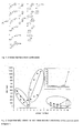
- Amines which can be used in the present invention are shown in the Figure 1.
- the chemical compound used in the present invention contains N-(4-methoxybenzyl)-(pyren-1-yl-methyl) amine or N-(benzyl)-(pyren-1-ylmethyl)amine.
- the chemical compound according to the invention is preferably soluble in an organic solvent so as to form a liquid phase etchant.
- the etch selectivity of the liquid etchant is preferably greater than 100 to 1, more preferably greater than 150 to 1.
- the chalcogenide glasses used in the present invention have at least one element in its chemical composition that belongs to the group VI of the periodic table, preferably S, Se, Te, in particular S.
- the present invention is directed to a method for fabricating 3-D nano-structures consisting of chalcogenide glass. According to that method the glass has been 3-D dimensionally photo-patterned via 3-D DLW (Direct Laser Writing).
- the above mentioned compound is used as etchant.
- the present invention is directed to N-(4-methoxybenzyl)-(pyren-1-yl-methyl)amine and N-(benzyl)-(pyren-1-ylmethyl)amine. These substance are the preferred etchants of the present invention.
- the chemical N-(4-methoxybenzyl)-(pyren-1-yl-methyl)amine, C16H9CH2NHCH2C6H5OCH3, is dissolved in a solution of 1.8 ml dimethylsulfoxide and 0.8 ml 1,2-dichloroethane at a concentration of 0.66 M (0.539 g). This solution is then mixed until it is homogenous and then it is poured into a shallow glass dish.
- the chalcogenide photoresist used here is arsenic trisulfide, As2S3, and it has been patterned in three-dimensions using the 3-D DLW method that was described in the earlier sections of this patent.
- this photoresist is first measured and recorded using a fiber interferometer. The film is then placed gently inside this solution and the shallow dish is covered with a watch glass. The film, here about 10 microns thick, is left soaking in the etchant, at room temperature, undisturbed for about 47 minutes. At the end of this time, one can visually see that the unexposed area of the photoresist, which has an orange-yellow color, is completely removed. This represents a etch rate of the unexposed areas, Ku, of 210 nm/ min. The film is taken out of the etchant and is rinsed with copious amount of acetone. The structures are then checked with a microscope.
- FIG. 3a shows light microscope and scanning electron micrographs of the structure after 5760 minutes (figure 3b and c), and they are essentially the same as at the time of 47 minutes. Therefore, theoretically, the etch rate is infinity. However for comparisons purposes, the time of 5760 minutes is taken as if the structures would have been totally removed. Hence the etch rate of the exposed area, Ke, for comparison purposes, is then 0.61 nm/min. Since the etch selectivity is the ratio of the Ku versus Ke, the etch selectivity in this case is at least 344 to 1.
- the chemical N-(benzyl)-(pyren-1-ylmethyl)amine, C6H6CH2NHCH2C16H9, is dissolved in a solution of 1.8 ml dimethylsulfoxide and 0.8 ml 1,2-dichloroethane at a concentration of 0.66 M (0.503 g). This solution is then mixed until it is homogenous and then it is poured into a shallow glass dish.
- the chalcogenide photoresist used here is arsenic trisulfide, As2S3, and it has been patterned in three-dimensions using the 3-D DLW method that was described in the earlier sections of this patent. The thickness of this photoresist is first measured and recorded using a fiber interferometer.
- the film is then placed gently inside this solution and the shallow dish is covered with a watch glass.
- the film here about 10 microns thick, is left soaking in the etchant, at room temperature, undisturbed for about 102 minutes.
- the unexposed area of the photoresist which has an orange-yellow color, is completely removed. This represents a etch rate of the unexposed areas, Ku, of 98 nm/ min.
- the film is taken out of the etchant and is rinsed with copious amount of acetone. The structures are then checked with a microscope.
- FIG. 3a shows light microscope and scanning electron micrographs of the structure after 3 days, or 4320 minutes (figure 3b and c), and they are essentially the same as at the time of 102 minutes. Therefore, theoretically, the etch rate is infinity. However for comparisons purposes, the time of 4320 minutes is taken as if the structures would have been totally removed. Hence the etch rate of the exposed area, Ke, for comparison purposes, is then 0.87 nm/min. Since the etch selectivity is the ratio of the Ku versus Ke, the etch selectivity in this case is 112 to 1.
- All 16 secondary benzylamine derivatives containing at least one benzyl group have been synthesized using a two-step synthesis. This consists of first forming an imine via the condensation coupling of an aldehyde and a primary amine, and then subsequently reducing the imine to obtain the final product.
- the etching solutions are all prepared by dissolving the amine in a solvent system of dimethylsulfoxide (dmso) and 1,2-dichloroethane (1,2-dce) at a concentration of 0.66 M.
- dmso dimethylsulfoxide
- 1,2-dce 1,2-dichloroethane
- the addition of small amounts of 1,2-dce serves to aid in the solvation of the larger non-polar amine molecules.
- the ratio of the 2 solvents was adjusted so that the Hildebrand constant of the overall solution has a value of 23.
- the direct laser written film is then placed in the etchant and periodically removed to count the rungs of the resulting 3D-nanostructures in the form of ladders with rungs that remain.
- the rate of dissolution of the unexposed areas (Ku) is defined as the amount of time that is required to completely dissolve all of the unexposed photoresist.
- the rate of dissolution of the exposed area (Ke) is the amount of time that is required to remove the rungs of the ladders in the 3-D structure.
- the overall etch selectivity ( ⁇ ) is then calculated as a ratio of these two etch rates (Ku / Ke).
- Figure 3 b to h shows scanning electron micrographs of some examples of different free-standing 3-D nanostructures that one could fabricate using the amine (13), when used in the method as described in the patent.
- Image b is the "step-ladder" test structure.
- Image c is a close up of the cross-section of a single rung of the ladder structure. It shows that smallest feature that is definable using this system is on the order of 170 nm.
- Image d is a 3-D array of spirals.
- Image e is a 3-D woodpile photonic crystal.
- Image f a 3-D array of fine spirals with individual feature sizes on the order of 170 nm.
- Image g is an array of nano-soccer balls.
- Image h is a close-up image of the soccer-ball.
- the nanostructures produced using this material and method possess exceptionally smooth and defect-free surfaces. Such aspects are critical for highly demanding applications of using nanostructures, such as those intended for optical applications
- the etching can be performed by doubling the concentration of (13) to 1.32 M.
- the result is that the etch rate of the unpolymerized areas has increased from 85 nm/s to 170 nm/s, a two-fold increase in the rate, while the polymerized areas remain un-etched after 96 hours.
Landscapes
- Chemical & Material Sciences (AREA)
- Organic Chemistry (AREA)
- Engineering & Computer Science (AREA)
- Physics & Mathematics (AREA)
- Life Sciences & Earth Sciences (AREA)
- Nanotechnology (AREA)
- Optics & Photonics (AREA)
- Biophysics (AREA)
- General Physics & Mathematics (AREA)
- Crystallography & Structural Chemistry (AREA)
- Microelectronics & Electronic Packaging (AREA)
- Chemical Kinetics & Catalysis (AREA)
- General Chemical & Material Sciences (AREA)
- Geochemistry & Mineralogy (AREA)
- Materials Engineering (AREA)
- Surface Treatment Of Glass (AREA)
- Manufacturing Optical Record Carriers (AREA)
Abstract
Description
- The present invention is related to the use of a chemical compound as an etchant for the removal of the unmodified areas of an imagewise modified chalcogenide based glass while leaving the modified areas un-removed. Furtheron the present invention is directed to a method for preparation of a free standing 3-D nano-structure by using the mentioned compound as well as to the compound as such.
- Chalcogenide glasses are materials that have at least one element in its chemical composition that belongs to group VI of the period table, namely the elements sulfur, selenium and tellurium. These chalcogenide glasses are able to be used as photo-resistive material.
- A resist material is known as a material that can have its chemical behavior modified via the exposure to an external stimulus. This stimulus could be induced by photons, electrons or other types of energy beams.
- One method to generate a photoinduced change in chalcogenide based glasses is the method of three-dimensional direct laser writing (3D-DLW). The method of 3-D DLW takes advantage of the fact that the method utilizes laser wavelengths that are below the bandgap of the photoresist material, so that one-photon absorption is negligible. What this means is that without focusing the laser radiation that is utilized, the beam can essentially pass through the material without being absorbed. However, if highly intense laser radiation is used, such as those generated from a femtosecond laser, and the laser beam is tightly focused into a very small spot, in the order of 200 nm, then the probability of the laser energy being absorbed via a two-photon process would likely occur. However, the absorption only occurs at the focus of the laser spot where the laser intensity is the highest, all other areas where the laser intensity is not focused will not be polymerized. This ability for the laser energy to be selectively absorbed in a three-dimensional space allows for the in-situ, or direct, generation of a three-dimensional image inside the photoresist. The images that are generated using the 3-D DLW method provide very tall, or thick, structures, with minimum feature sizes below 200 nm, directly inside the photoresist. To etch out, or reveal this structure then requires a highly selective chemical etchant that allows for the total removal of the unexposed areas, while leaving the exposed areas behind.
- A liquid etchant is generally defined as a chemical solution that is able to controllably remove a solid material. When such an etchant is used in the field of resists, it has the meaning that it possesses the ability to controllably remove areas that have not been modified using an external stimulus, (ie. photons, electron beams, etc), over that of those areas that have been modified using an external stimulus, or vice versa. In the instance described in the following, the removal of the unmodified areas over that of the modified areas serves to provide a negative image of the laser-beam or photomask, therefore this etchant is a negative tone etchant.
- Liquid etchants for chalcogenide glasses have been formulated to take advantage of the fact that there is a chemical difference that arises in chalcogenide-based glasses after exposure to an external stimulus. There are two main types of liquid etchants that are known in the scientific and patent literature which etch chalcogenide-based glasses. These two types mainly differ by the solvent systems that they employ. The first type are water-based (aqueous), and the second are organic solvent based etchants.
- In the aqueous based etchants, the active component in their composition is usually an inorganic base which generates a basic condition (pH> 7) using anions such as hydroxide, sulfides, sulfites, disulfides, amines and cyanides. The basic environment creates oxidizing conditions which oxidize the components in the chalcogenide glass into water-soluble species, and thereby dissolving them in the aqueous phase. Additives such as surfactants are also added to increase the selectivity of the etchant composition. It has been shown that etchants containing these species are able to etch chalcogenide-glasses with some selectivity but they have only been shown to be confined to etching very thin films with structures having a height of no more than 500 nm. This is due to the fact that the oxidizing conditions are so strong, that all of the material whether modified or not, will be completely removed after a short time.
- In the organic based etchants, the active components in its composition is usually a short chain amine, C < 5, that is dissolved in an organic solvent. These compositions have also been shown to reveal thin 2-D structures usually no more than 500 nm thick. The organic amine again acts as an oxidant to oxidize the species in the chalcogenide-based glasses. Only very thin structures are made because the oxidizing conditions are again so strong that all of the material is removed, and hence the reaction is essentially kinetically controlled.
- It has been shown that the photosensitive V-VI semiconducting chalcogenide glass, As2S3, is also compatible with the 3-D DLW process. But the etching chemistry in As2S3 is not developed well enough to take full advantage of the precision placement of 3-D features, and sub-diffraction limit resolution, that the 3-D DLW method routinely achieves in organic photopolymers (Wong et al. Adv. Mater. (2006), 18, pg 265-269).
- The problem that was noticed earlier on when fabricating 3-D structures on the nanoscale was that the demands on the etchant's selectivity (y), becomes much greater than for 2-D structures. The selectivity of an etchant (y), is defined as the ratio between the rate of the unexposed areas (Ku) and the rate of the removal of the exposed areas (Ke). Therefore, when developing As2S3 as a negative-tone photoresist, the unexposed areas should be removed as quickly as possible, while the exposed areas should remain as long as possible, so as to afford a large y. A large y will allow thick structures with fine resolution to be produced.
- The first demand on a etchant system that requires a large γ, stems from the fact that 3-D structures must be immersed for a longer period of time in the etchant to develop its structures. This is a result of the slower diffusion of liquid etchants though a more obstructed nano-porous structure. Another demand is due to the higher reaction rate on the areas that have already been developed by the etchant in 3-D structures. This is because the surface area of a porous 3-D structure is much larger than the surface area of a 2-D structure of the same volume. Therefore, the etch selectivity of the etchant that is employed to directly develop a 3-D structure, must be significantly higher in the 3-D case than the 2-D case. Currently available etchant studies found in the literature (A.Feigel et al. Applied Physics letters (2003), 83, pg 4480.) that deal with As2S3 as a photoresist, are only investigated to be applied to fabricate thin 2-D structures less than 500 nm in height. There, the etch selectivity requirements are much lower. Functional 3-D structures (such as 3-D PBG materials, or nano and micro-machines) often require structures with a height of 20 microns or more. Therefore, the demands placed on the etch selectivity of the etchant composition for direct 3-D fabrication of 3-D nano-structures are much greater.
- Therefore, the etchants that are currently available fail greatly when they are employed to etch thick 3-D structures generated via 3-D DLW. This is because those compositions found in the open literature (S.A. Zenkin et al. Glass Physics and Chemistry (1997), 5, pg 393, A. Feigel et al. Applied Phscis Letters, (2000) 77, pg 3221.) are used to etch thin 2-D structures, where the selectivity requirement is much lower. Accordingly an etchant composition that is tailored to fulfil the requirements of a highly selective etchant to etch thick 2-D and 3-D structures generated via 3-D DLW is required.
- Accordingly the present invention is directed to the use of a chemical compound as etchant for the removal of the un-modified areas of a chalcogenide-based glass while leaving the modified areas un-removed, whereby said compound contains a secondary amine R1R2NH with R1 and/or R2 having a sterically bulky group with more than 5 atoms.
- The invention that is presented here relates to an etching composition that contains a family of bulky organic secondary amine molecules, R1R2NH, which when used as the main component in an etchant, provides a high selectivity that is required to produce 2-D and 3-D etched articles using chalcogenide-based glasses. The ability of such an etchant described herein to provide a high etch selectivity rests entirely on the steric properties of the R groups of the secondary amine molecule itself. More specifically, the secondary amine molecule that is used here must have R groups containing 5 or more atoms. Such a molecule, when dissolved in an organic solvent, has the ability to selectively remove the un-modified areas of a chalcogenide based-glass while preventing the removal of the exposed areas of the chalcogenide-based photoresist. The use of such an etching composition allows thick, or tall, two- or three-dimensional articles to be fabricated from chalcogenide-based glasses using 3-D DLW.
- Particularly R1 and R2 are most preferred but not limited to, benzyl-, napthyl-, pyrenyl-, pyridinyl-, isoamyl-, anthracyl-, and boranes. The atoms are preferably selected from the groups carbon, boron and nitrogen, in particular carbon.
- In a most preferred form of the present invention R is an aryl group.
- Secondary amines containing at least one benzyl group are preferably used. Examples of advantageous secondary amines containing at least one benzyl group are dibenzylamine and N-(4-fluorobenyzl)-benzylamine.
Examples of Amines which can be used in the present invention are shown in the Figure 1. - Most preferably the chemical compound used in the present invention contains N-(4-methoxybenzyl)-(pyren-1-yl-methyl) amine or N-(benzyl)-(pyren-1-ylmethyl)amine.
- The chemical compound according to the invention is preferably soluble in an organic solvent so as to form a liquid phase etchant.
- The etch selectivity of the liquid etchant is preferably greater than 100 to 1, more preferably greater than 150 to 1.
The chalcogenide glasses used in the present invention have at least one element in its chemical composition that belongs to the group VI of the periodic table, preferably S, Se, Te, in particular S. - Further on the present invention is directed to a method for fabricating 3-D nano-structures consisting of chalcogenide glass. According to that method the glass has been 3-D dimensionally photo-patterned via 3-D DLW (Direct Laser Writing).
- Thereafter the unmodified areas are removed. In the present invention the above mentioned compound is used as etchant.
- Finally the present invention is directed to N-(4-methoxybenzyl)-(pyren-1-yl-methyl)amine and N-(benzyl)-(pyren-1-ylmethyl)amine. These substance are the preferred etchants of the present invention.
- The subject matter of the present invention i s explained in the following three examples:
- The chemical N-(4-methoxybenzyl)-(pyren-1-yl-methyl)amine, C16H9CH2NHCH2C6H5OCH3, is dissolved in a solution of 1.8 ml dimethylsulfoxide and 0.8
ml 1,2-dichloroethane at a concentration of 0.66 M (0.539 g). This solution is then mixed until it is homogenous and then it is poured into a shallow glass dish. The chalcogenide photoresist used here is arsenic trisulfide, As2S3, and it has been patterned in three-dimensions using the 3-D DLW method that was described in the earlier sections of this patent. The thickness of this photoresist is first measured and recorded using a fiber interferometer. The film is then placed gently inside this solution and the shallow dish is covered with a watch glass. The film, here about 10 microns thick, is left soaking in the etchant, at room temperature, undisturbed for about 47 minutes. At the end of this time, one can visually see that the unexposed area of the photoresist, which has an orange-yellow color, is completely removed. This represents a etch rate of the unexposed areas, Ku, of 210 nm/ min. The film is taken out of the etchant and is rinsed with copious amount of acetone. The structures are then checked with a microscope. - The structure is then replaced into the etchant and is allowed to soak for 4 days or 5760 minutes. At the end of this time, the substrate with the structures are once again removed and rinsed with copious amounts of acetone and then placed under the microscope. Figure 3a shows light microscope and scanning electron micrographs of the structure after 5760 minutes (figure 3b and c), and they are essentially the same as at the time of 47 minutes. Therefore, theoretically, the etch rate is infinity. However for comparisons purposes, the time of 5760 minutes is taken as if the structures would have been totally removed. Hence the etch rate of the exposed area, Ke, for comparison purposes, is then 0.61 nm/min. Since the etch selectivity is the ratio of the Ku versus Ke, the etch selectivity in this case is at least 344 to 1.
- The chemical N-(benzyl)-(pyren-1-ylmethyl)amine, C6H6CH2NHCH2C16H9, is dissolved in a solution of 1.8 ml dimethylsulfoxide and 0.8
ml 1,2-dichloroethane at a concentration of 0.66 M (0.503 g). This solution is then mixed until it is homogenous and then it is poured into a shallow glass dish. The chalcogenide photoresist used here is arsenic trisulfide, As2S3, and it has been patterned in three-dimensions using the 3-D DLW method that was described in the earlier sections of this patent. The thickness of this photoresist is first measured and recorded using a fiber interferometer. The film is then placed gently inside this solution and the shallow dish is covered with a watch glass. The film, here about 10 microns thick, is left soaking in the etchant, at room temperature, undisturbed for about 102 minutes. At the end of this time, one can visually see that the unexposed area of the photoresist, which has an orange-yellow color, is completely removed. This represents a etch rate of the unexposed areas, Ku, of 98 nm/ min. The film is taken out of the etchant and is rinsed with copious amount of acetone. The structures are then checked with a microscope. - The structure is then replaced into the etchant and is allowed to soak for 3 days or 4320 minutes. At the end of this time, the substrate with the structures are once again removed and rinsed with copious amounts of acetone and then placed under the microscope. Figure 3a shows light microscope and scanning electron micrographs of the structure after 3 days, or 4320 minutes (figure 3b and c), and they are essentially the same as at the time of 102 minutes. Therefore, theoretically, the etch rate is infinity. However for comparisons purposes, the time of 4320 minutes is taken as if the structures would have been totally removed. Hence the etch rate of the exposed area, Ke, for comparison purposes, is then 0.87 nm/min. Since the etch selectivity is the ratio of the Ku versus Ke, the etch selectivity in this case is 112 to 1.
- All 16 secondary benzylamine derivatives containing at least one benzyl group (see figure 1) have been synthesized using a two-step synthesis. This consists of first forming an imine via the condensation coupling of an aldehyde and a primary amine, and then subsequently reducing the imine to obtain the final product.
- To ensure that the same conditions for the comparison between the different secondary amines are used, the etching solutions are all prepared by dissolving the amine in a solvent system of dimethylsulfoxide (dmso) and 1,2-dichloroethane (1,2-dce) at a concentration of 0.66 M. We chose dmso as the solvent because it is a good solvent for
S N2 type reactions. The addition of small amounts of 1,2-dce serves to aid in the solvation of the larger non-polar amine molecules. The ratio of the 2 solvents was adjusted so that the Hildebrand constant of the overall solution has a value of 23. The direct laser written film is then placed in the etchant and periodically removed to count the rungs of the resulting 3D-nanostructures in the form of ladders with rungs that remain. The rate of dissolution of the unexposed areas (Ku) is defined as the amount of time that is required to completely dissolve all of the unexposed photoresist. The rate of dissolution of the exposed area (Ke) is the amount of time that is required to remove the rungs of the ladders in the 3-D structure. The overall etch selectivity (γ) is then calculated as a ratio of these two etch rates (Ku / Ke). - Figure 3 b to h shows scanning electron micrographs of some examples of different free-standing 3-D nanostructures that one could fabricate using the amine (13), when used in the method as described in the patent. Image b, is the "step-ladder" test structure. Image c, is a close up of the cross-section of a single rung of the ladder structure. It shows that smallest feature that is definable using this system is on the order of 170 nm. Image d, is a 3-D array of spirals. Image e, is a 3-D woodpile photonic crystal. Image f, a 3-D array of fine spirals with individual feature sizes on the order of 170 nm. Image g, is an array of nano-soccer balls. Image h, is a close-up image of the soccer-ball. One should notice that the nanostructures produced using this material and method, possess exceptionally smooth and defect-free surfaces. Such aspects are critical for highly demanding applications of using nanostructures, such as those intended for optical applications.
- On surveying the data tabulated in the following table, there is almost a 100 fold increase in the etch selectivity on synthetically exchanging one of the benzyl arm that is present in molecule (1) to a pyrenyl arm of (14).
Table. Summary of the etch selectivity (γ) and etch rate of all of the dibenzylamine derivatives synthesized. Amine identity Ku (nm/min) Ke (nm/min) Selectivity (γ) 1 476 379 1.26 2 306 212 1.44 3 207 114 1.81 4 188 30 6.27 5 513 219 2.34 6 826 304 2.72 7 1020 349 2.92 8 No reaction No reaction - 9 No reaction No reaction - 10 No reaction No reaction - 11 111 33 3.36 12 84.7 5.02 16.87 13 59.7 5.31 11.24 14 98 0.87 113.79 15 No reaction No reaction - 16 210 0.61 344.26 triethylamine No reaction No reaction - - Further on the etching can be performed by doubling the concentration of (13) to 1.32 M. The result is that the etch rate of the unpolymerized areas has increased from 85 nm/s to 170 nm/s, a two-fold increase in the rate, while the polymerized areas remain un-etched after 96 hours.
- In
molecule 13 both arms of the amine have been modified to napthyl- groups. Although the Ku has decreased as expected, the selectivity has not improved. - With regard to the novel amine, N-(4-methoxybenzyl)-(pyren-1-yl)amine (16) a high etch selectivity (γ=344) is obtained.
Claims (14)
- Use of a chemical compound as an etchant for the removal of the unmodified areas of a chalcogenide-based glass, while leaving the image wise modified areas un-removed, whereby said compound contains a secondary amine, R1 R2 NH, with R1 and/or R2 having a sterically bulky group with more than 5 atoms.
- Use according to claim 1,
characterized in that the liquid etchant should selectively etch any glass composition that contains elements from group VI of the period table. - Use according to claim 1 or 2,
characterized in that the glass composition contains S, Se and Te. - Use according to one of the claims 1 to 3,
characterized in that the modified areas are made via imagewise exposure. - Use according to one of the claims 1 to 4,
characterized in that the glass composition is a photo-patterned photo-resist. - Use according to one of the claims 1 to 5,
characterized in that photoinduced changes in the chalcogenide glasses are generated by 3-D dimensional direct laser writing. - Use according to one of the claims 1 to 6,
characterized in that R1 R2 are preferred but not limited to, benzyl-, napthyl-, pyrenyl-, pyridinyl-, isoamyl-, anthracyl-, and boranes. - Use according to one of the claims 1 to 7,
characterized in that the atoms are selected from the group carbon, boron, nitrogen. - Use according to one of the claims 1 to 8,
characterized in that R is an aryl group. - Use according to one of the claims 1 to 9,
characterized in that the molecule is N-(4-methoxybenzyl)-(pyren-1-yl-methyl)amine or N-(benzyl)-(pyren-1-ylmethyl)amine. - Use according to one the claims 1 to 10,
characterized in that the molecule is soluble in an organic solvent so as to form a liquid phase etchant. - Method for fabricating the 3-D nano-structures consisting of chalcogenide glass,
characterized in that the glass is three -dimensionally photo-patterned via 3-D DLW and that the unmodified areas are thereafter removed by using the etching agent defined in one of the claims 7 to 11. - N-(4-methoxybenzyl)-(pyren-1-yl-methyl)amine.
- N-(benzyl)-(pyren-1-ylmethyl)amine.
Priority Applications (3)
| Application Number | Priority Date | Filing Date | Title |
|---|---|---|---|
| EP06122987.8A EP1918261B1 (en) | 2006-10-26 | 2006-10-26 | Chemical etching composition for the preparation of 3-d nanostructures |
| CA2607781A CA2607781C (en) | 2006-10-26 | 2007-10-11 | Chemical etching composition for the preparation of 3-d nano-structures |
| US11/978,225 US7938980B2 (en) | 2006-10-26 | 2007-10-26 | Chemical etching composition for the preparation of 3-D nano-structures |
Applications Claiming Priority (1)
| Application Number | Priority Date | Filing Date | Title |
|---|---|---|---|
| EP06122987.8A EP1918261B1 (en) | 2006-10-26 | 2006-10-26 | Chemical etching composition for the preparation of 3-d nanostructures |
Publications (2)
| Publication Number | Publication Date |
|---|---|
| EP1918261A1 true EP1918261A1 (en) | 2008-05-07 |
| EP1918261B1 EP1918261B1 (en) | 2016-09-07 |
Family
ID=37854794
Family Applications (1)
| Application Number | Title | Priority Date | Filing Date |
|---|---|---|---|
| EP06122987.8A Not-in-force EP1918261B1 (en) | 2006-10-26 | 2006-10-26 | Chemical etching composition for the preparation of 3-d nanostructures |
Country Status (3)
| Country | Link |
|---|---|
| US (1) | US7938980B2 (en) |
| EP (1) | EP1918261B1 (en) |
| CA (1) | CA2607781C (en) |
Families Citing this family (7)
| Publication number | Priority date | Publication date | Assignee | Title |
|---|---|---|---|---|
| KR20130106770A (en) * | 2010-07-26 | 2013-09-30 | 하마마츠 포토닉스 가부시키가이샤 | Method for manufacturing semiconductor device |
| CN111087182A (en) * | 2020-01-10 | 2020-05-01 | 宁波大学 | Chemical corrosion preparation method of chalcogenide glass tapered optical fiber |
| WO2023046901A1 (en) | 2021-09-24 | 2023-03-30 | Analog Devices International Unlimited Company, | Magnetic field sensing based on particle position within container |
| US11940502B2 (en) | 2021-09-24 | 2024-03-26 | Analog Devices International Unlimited Company | Magnetic field sensing based on particle position within container |
| US12613147B2 (en) | 2021-11-12 | 2026-04-28 | Analog Devices International Unlimited Company | Temperature sensing with particles in medium material |
| US12435803B2 (en) | 2022-05-27 | 2025-10-07 | Analog Devices International Unlimited Company | Flow adjustment based on particle movement in response to magnetic field |
| US12379433B2 (en) | 2022-09-14 | 2025-08-05 | Analog Devices International Unlimited Company | Magnetically sensitive particles and magnetic structure |
Citations (1)
| Publication number | Priority date | Publication date | Assignee | Title |
|---|---|---|---|---|
| US4405710A (en) * | 1981-06-22 | 1983-09-20 | Cornell Research Foundation, Inc. | Ion beam exposure of (g-Gex -Se1-x) inorganic resists |
Family Cites Families (1)
| Publication number | Priority date | Publication date | Assignee | Title |
|---|---|---|---|---|
| JPH11139846A (en) * | 1997-11-04 | 1999-05-25 | Shipley Far East Kk | Photosensitive glass paste |
-
2006
- 2006-10-26 EP EP06122987.8A patent/EP1918261B1/en not_active Not-in-force
-
2007
- 2007-10-11 CA CA2607781A patent/CA2607781C/en not_active Expired - Fee Related
- 2007-10-26 US US11/978,225 patent/US7938980B2/en not_active Expired - Fee Related
Patent Citations (1)
| Publication number | Priority date | Publication date | Assignee | Title |
|---|---|---|---|---|
| US4405710A (en) * | 1981-06-22 | 1983-09-20 | Cornell Research Foundation, Inc. | Ion beam exposure of (g-Gex -Se1-x) inorganic resists |
Non-Patent Citations (3)
| Title |
|---|
| FEIGEL A ET AL: "CHALCOGENIDE GLASS-BASED THREE-DIMENSIONAL PHOTONIC CRYSTALS", APPLIED PHYSICS LETTERS, AIP, AMERICAN INSTITUTE OF PHYSICS, MELVILLE, NY, US, vol. 77, no. 20, 13 November 2000 (2000-11-13), pages 3221 - 3223, XP000970295, ISSN: 0003-6951 * |
| LODEIRO, C. ET AL: "Intramolecular excimer formation and sensing behavior of new fluorimetric probes and their interactions with metal cations and barbituric acids", SENSORS AND ACTUATORS, B: CHEMICAL , B115(1), 276-286 CODEN: SABCEB; ISSN: 0925-4005, 28 October 2005 (2005-10-28), XP002435735 * |
| ZAHARESCU T ET AL: "Effects of some secondary amines on the oxidation of ethylene-propylene elastomers", POLYMER DEGRADATION AND STABILITY, BARKING, GB, vol. 68, no. 1, 1 April 2000 (2000-04-01), pages 83 - 86, XP004294916, ISSN: 0141-3910 * |
Also Published As
| Publication number | Publication date |
|---|---|
| US20080128391A1 (en) | 2008-06-05 |
| EP1918261B1 (en) | 2016-09-07 |
| CA2607781C (en) | 2014-09-16 |
| US7938980B2 (en) | 2011-05-10 |
| CA2607781A1 (en) | 2008-04-26 |
Similar Documents
| Publication | Publication Date | Title |
|---|---|---|
| CA2607781C (en) | Chemical etching composition for the preparation of 3-d nano-structures | |
| DE69930832T2 (en) | USE OF A COMPOSITION FOR AN ANTI-REFLECTIVE LAYER | |
| TWI374342B (en) | Water soluble resin composition and method for pattern formation using the same | |
| DE69709874T2 (en) | AQUEOUS ANTIREFLEX COATING FOR PHOTORESIST COMPOSITIONS | |
| DE69726378T2 (en) | Colored photoresists and methods and articles incorporating them | |
| KR101253412B1 (en) | Dithiane derivative, polymer, resist composition, and process for producing semiconductor using the resist composition | |
| US5635332A (en) | Alkylsulfonium salts and photoresist compositions containing the same | |
| EP2905803B1 (en) | Method for cleaning and drying semiconductor substrate | |
| DE69624085T2 (en) | Chemically enhanced positive photoresists | |
| DE69130125T3 (en) | Positive-working photoresist composition | |
| TW201110195A (en) | Methods of forming electronic devices | |
| DE112009000979T5 (en) | Photosensitive hardmask for microlithography | |
| DE69031785T2 (en) | Photosensitive composition | |
| DE19912047A1 (en) | Negative resist composition useful in microlithography for producing (very) large scale integrated circuits | |
| CA1272059A (en) | Negative photoresist systems | |
| US7419759B2 (en) | Photoresist composition and method of forming a pattern using the same | |
| JP2006072329A (en) | Composition of upper antireflection film and pattern forming method of semiconductor device using the same | |
| CA2406219A1 (en) | Radiation sensitive refractive index changing composition | |
| DE4207264A1 (en) | Negative-working radiation-sensitive mixt. - contg. reactive binder with 2,2,2-tri:fluoro-1-hydroxy-1-tri:fluoro-methyl-ethyl gps., photo-acid and crosslinking cpd., useful e.g. as photoresist | |
| JPH03223867A (en) | Pattern forming method | |
| DE4112970A1 (en) | Acid-cleavable radiation-sensitive compounds, the radiation-sensitive mixture containing them and radiation radiation-sensitive material made from them | |
| US8134684B2 (en) | Immersion lithography using hafnium-based nanoparticles | |
| US7282319B2 (en) | Photoresist composition and method of forming a pattern using same | |
| KR100764392B1 (en) | Ultrafine pattern formation method using organic diffuse reflection prevention film containing thermal acid generator | |
| US7390611B2 (en) | Photoresist coating composition and method for forming fine pattern using the same |
Legal Events
| Date | Code | Title | Description |
|---|---|---|---|
| PUAI | Public reference made under article 153(3) epc to a published international application that has entered the european phase |
Free format text: ORIGINAL CODE: 0009012 |
|
| AK | Designated contracting states |
Kind code of ref document: A1 Designated state(s): AT BE BG CH CY CZ DE DK EE ES FI FR GB GR HU IE IS IT LI LT LU LV MC NL PL PT RO SE SI SK TR |
|
| AX | Request for extension of the european patent |
Extension state: AL BA HR MK RS |
|
| 17P | Request for examination filed |
Effective date: 20080625 |
|
| AKX | Designation fees paid |
Designated state(s): AT BE BG CH CY CZ DE DK EE ES FI FR GB GR HU IE IS IT LI LT LU LV MC NL PL PT RO SE SI SK TR |
|
| 17Q | First examination report despatched |
Effective date: 20081223 |
|
| RAP1 | Party data changed (applicant data changed or rights of an application transferred) |
Owner name: KARLSRUHER INSTITUT FUER TECHNOLOGIE |
|
| GRAP | Despatch of communication of intention to grant a patent |
Free format text: ORIGINAL CODE: EPIDOSNIGR1 |
|
| INTG | Intention to grant announced |
Effective date: 20160404 |
|
| GRAS | Grant fee paid |
Free format text: ORIGINAL CODE: EPIDOSNIGR3 |
|
| GRAA | (expected) grant |
Free format text: ORIGINAL CODE: 0009210 |
|
| AK | Designated contracting states |
Kind code of ref document: B1 Designated state(s): AT BE BG CH CY CZ DE DK EE ES FI FR GB GR HU IE IS IT LI LT LU LV MC NL PL PT RO SE SI SK TR |
|
| REG | Reference to a national code |
Ref country code: GB Ref legal event code: FG4D |
|
| REG | Reference to a national code |
Ref country code: CH Ref legal event code: EP |
|
| REG | Reference to a national code |
Ref country code: IE Ref legal event code: FG4D |
|
| REG | Reference to a national code |
Ref country code: AT Ref legal event code: REF Ref document number: 826681 Country of ref document: AT Kind code of ref document: T Effective date: 20161015 |
|
| REG | Reference to a national code |
Ref country code: DE Ref legal event code: R096 Ref document number: 602006050185 Country of ref document: DE |
|
| REG | Reference to a national code |
Ref country code: LT Ref legal event code: MG4D |
|
| REG | Reference to a national code |
Ref country code: NL Ref legal event code: MP Effective date: 20160907 |
|
| PG25 | Lapsed in a contracting state [announced via postgrant information from national office to epo] |
Ref country code: FI Free format text: LAPSE BECAUSE OF FAILURE TO SUBMIT A TRANSLATION OF THE DESCRIPTION OR TO PAY THE FEE WITHIN THE PRESCRIBED TIME-LIMIT Effective date: 20160907 Ref country code: LT Free format text: LAPSE BECAUSE OF FAILURE TO SUBMIT A TRANSLATION OF THE DESCRIPTION OR TO PAY THE FEE WITHIN THE PRESCRIBED TIME-LIMIT Effective date: 20160907 |
|
| REG | Reference to a national code |
Ref country code: AT Ref legal event code: MK05 Ref document number: 826681 Country of ref document: AT Kind code of ref document: T Effective date: 20160907 |
|
| PG25 | Lapsed in a contracting state [announced via postgrant information from national office to epo] |
Ref country code: NL Free format text: LAPSE BECAUSE OF FAILURE TO SUBMIT A TRANSLATION OF THE DESCRIPTION OR TO PAY THE FEE WITHIN THE PRESCRIBED TIME-LIMIT Effective date: 20160907 Ref country code: LV Free format text: LAPSE BECAUSE OF FAILURE TO SUBMIT A TRANSLATION OF THE DESCRIPTION OR TO PAY THE FEE WITHIN THE PRESCRIBED TIME-LIMIT Effective date: 20160907 Ref country code: BE Free format text: LAPSE BECAUSE OF NON-PAYMENT OF DUE FEES Effective date: 20161031 Ref country code: GR Free format text: LAPSE BECAUSE OF FAILURE TO SUBMIT A TRANSLATION OF THE DESCRIPTION OR TO PAY THE FEE WITHIN THE PRESCRIBED TIME-LIMIT Effective date: 20161208 Ref country code: ES Free format text: LAPSE BECAUSE OF FAILURE TO SUBMIT A TRANSLATION OF THE DESCRIPTION OR TO PAY THE FEE WITHIN THE PRESCRIBED TIME-LIMIT Effective date: 20160907 Ref country code: SE Free format text: LAPSE BECAUSE OF FAILURE TO SUBMIT A TRANSLATION OF THE DESCRIPTION OR TO PAY THE FEE WITHIN THE PRESCRIBED TIME-LIMIT Effective date: 20160907 |
|
| PG25 | Lapsed in a contracting state [announced via postgrant information from national office to epo] |
Ref country code: EE Free format text: LAPSE BECAUSE OF FAILURE TO SUBMIT A TRANSLATION OF THE DESCRIPTION OR TO PAY THE FEE WITHIN THE PRESCRIBED TIME-LIMIT Effective date: 20160907 Ref country code: RO Free format text: LAPSE BECAUSE OF FAILURE TO SUBMIT A TRANSLATION OF THE DESCRIPTION OR TO PAY THE FEE WITHIN THE PRESCRIBED TIME-LIMIT Effective date: 20160907 |
|
| PG25 | Lapsed in a contracting state [announced via postgrant information from national office to epo] |
Ref country code: AT Free format text: LAPSE BECAUSE OF FAILURE TO SUBMIT A TRANSLATION OF THE DESCRIPTION OR TO PAY THE FEE WITHIN THE PRESCRIBED TIME-LIMIT Effective date: 20160907 Ref country code: SK Free format text: LAPSE BECAUSE OF FAILURE TO SUBMIT A TRANSLATION OF THE DESCRIPTION OR TO PAY THE FEE WITHIN THE PRESCRIBED TIME-LIMIT Effective date: 20160907 Ref country code: BE Free format text: LAPSE BECAUSE OF FAILURE TO SUBMIT A TRANSLATION OF THE DESCRIPTION OR TO PAY THE FEE WITHIN THE PRESCRIBED TIME-LIMIT Effective date: 20160907 Ref country code: PT Free format text: LAPSE BECAUSE OF FAILURE TO SUBMIT A TRANSLATION OF THE DESCRIPTION OR TO PAY THE FEE WITHIN THE PRESCRIBED TIME-LIMIT Effective date: 20170109 Ref country code: IS Free format text: LAPSE BECAUSE OF FAILURE TO SUBMIT A TRANSLATION OF THE DESCRIPTION OR TO PAY THE FEE WITHIN THE PRESCRIBED TIME-LIMIT Effective date: 20170107 Ref country code: CZ Free format text: LAPSE BECAUSE OF FAILURE TO SUBMIT A TRANSLATION OF THE DESCRIPTION OR TO PAY THE FEE WITHIN THE PRESCRIBED TIME-LIMIT Effective date: 20160907 Ref country code: BG Free format text: LAPSE BECAUSE OF FAILURE TO SUBMIT A TRANSLATION OF THE DESCRIPTION OR TO PAY THE FEE WITHIN THE PRESCRIBED TIME-LIMIT Effective date: 20161207 Ref country code: PL Free format text: LAPSE BECAUSE OF FAILURE TO SUBMIT A TRANSLATION OF THE DESCRIPTION OR TO PAY THE FEE WITHIN THE PRESCRIBED TIME-LIMIT Effective date: 20160907 |
|
| REG | Reference to a national code |
Ref country code: CH Ref legal event code: PL |
|
| REG | Reference to a national code |
Ref country code: DE Ref legal event code: R097 Ref document number: 602006050185 Country of ref document: DE |
|
| PG25 | Lapsed in a contracting state [announced via postgrant information from national office to epo] |
Ref country code: IT Free format text: LAPSE BECAUSE OF FAILURE TO SUBMIT A TRANSLATION OF THE DESCRIPTION OR TO PAY THE FEE WITHIN THE PRESCRIBED TIME-LIMIT Effective date: 20160907 |
|
| PLBE | No opposition filed within time limit |
Free format text: ORIGINAL CODE: 0009261 |
|
| STAA | Information on the status of an ep patent application or granted ep patent |
Free format text: STATUS: NO OPPOSITION FILED WITHIN TIME LIMIT |
|
| REG | Reference to a national code |
Ref country code: IE Ref legal event code: MM4A |
|
| REG | Reference to a national code |
Ref country code: FR Ref legal event code: ST Effective date: 20170630 |
|
| PG25 | Lapsed in a contracting state [announced via postgrant information from national office to epo] |
Ref country code: FR Free format text: LAPSE BECAUSE OF NON-PAYMENT OF DUE FEES Effective date: 20161107 Ref country code: DK Free format text: LAPSE BECAUSE OF FAILURE TO SUBMIT A TRANSLATION OF THE DESCRIPTION OR TO PAY THE FEE WITHIN THE PRESCRIBED TIME-LIMIT Effective date: 20160907 Ref country code: LI Free format text: LAPSE BECAUSE OF NON-PAYMENT OF DUE FEES Effective date: 20161031 Ref country code: CH Free format text: LAPSE BECAUSE OF NON-PAYMENT OF DUE FEES Effective date: 20161031 |
|
| 26N | No opposition filed |
Effective date: 20170608 |
|
| GBPC | Gb: european patent ceased through non-payment of renewal fee |
Effective date: 20161207 |
|
| PG25 | Lapsed in a contracting state [announced via postgrant information from national office to epo] |
Ref country code: LU Free format text: LAPSE BECAUSE OF NON-PAYMENT OF DUE FEES Effective date: 20161026 Ref country code: SI Free format text: LAPSE BECAUSE OF FAILURE TO SUBMIT A TRANSLATION OF THE DESCRIPTION OR TO PAY THE FEE WITHIN THE PRESCRIBED TIME-LIMIT Effective date: 20160907 |
|
| PG25 | Lapsed in a contracting state [announced via postgrant information from national office to epo] |
Ref country code: IE Free format text: LAPSE BECAUSE OF NON-PAYMENT OF DUE FEES Effective date: 20161026 Ref country code: GB Free format text: LAPSE BECAUSE OF NON-PAYMENT OF DUE FEES Effective date: 20161207 |
|
| PG25 | Lapsed in a contracting state [announced via postgrant information from national office to epo] |
Ref country code: CY Free format text: LAPSE BECAUSE OF FAILURE TO SUBMIT A TRANSLATION OF THE DESCRIPTION OR TO PAY THE FEE WITHIN THE PRESCRIBED TIME-LIMIT Effective date: 20160907 Ref country code: HU Free format text: LAPSE BECAUSE OF FAILURE TO SUBMIT A TRANSLATION OF THE DESCRIPTION OR TO PAY THE FEE WITHIN THE PRESCRIBED TIME-LIMIT; INVALID AB INITIO Effective date: 20061026 |
|
| PG25 | Lapsed in a contracting state [announced via postgrant information from national office to epo] |
Ref country code: MC Free format text: LAPSE BECAUSE OF FAILURE TO SUBMIT A TRANSLATION OF THE DESCRIPTION OR TO PAY THE FEE WITHIN THE PRESCRIBED TIME-LIMIT Effective date: 20160907 Ref country code: TR Free format text: LAPSE BECAUSE OF FAILURE TO SUBMIT A TRANSLATION OF THE DESCRIPTION OR TO PAY THE FEE WITHIN THE PRESCRIBED TIME-LIMIT Effective date: 20160907 |
|
| PGFP | Annual fee paid to national office [announced via postgrant information from national office to epo] |
Ref country code: DE Payment date: 20181024 Year of fee payment: 13 |
|
| REG | Reference to a national code |
Ref country code: DE Ref legal event code: R082 Ref document number: 602006050185 Country of ref document: DE |
|
| REG | Reference to a national code |
Ref country code: DE Ref legal event code: R119 Ref document number: 602006050185 Country of ref document: DE |
|
| PG25 | Lapsed in a contracting state [announced via postgrant information from national office to epo] |
Ref country code: DE Free format text: LAPSE BECAUSE OF NON-PAYMENT OF DUE FEES Effective date: 20200501 |