EP1914833A1 - Decoupling arrays of radiating elements of an antenna - Google Patents
Decoupling arrays of radiating elements of an antenna Download PDFInfo
- Publication number
- EP1914833A1 EP1914833A1 EP07117631A EP07117631A EP1914833A1 EP 1914833 A1 EP1914833 A1 EP 1914833A1 EP 07117631 A EP07117631 A EP 07117631A EP 07117631 A EP07117631 A EP 07117631A EP 1914833 A1 EP1914833 A1 EP 1914833A1
- Authority
- EP
- European Patent Office
- Prior art keywords
- antenna
- arrays
- antenna according
- radiating elements
- planes
- Prior art date
- Legal status (The legal status is an assumption and is not a legal conclusion. Google has not performed a legal analysis and makes no representation as to the accuracy of the status listed.)
- Withdrawn
Links
- 238000003491 array Methods 0.000 title claims abstract description 24
- 239000002184 metal Substances 0.000 claims abstract description 13
- 229910052751 metal Inorganic materials 0.000 claims abstract description 13
- 238000004519 manufacturing process Methods 0.000 claims description 4
- 230000008878 coupling Effects 0.000 description 4
- 238000010168 coupling process Methods 0.000 description 4
- 238000005859 coupling reaction Methods 0.000 description 4
- 230000005540 biological transmission Effects 0.000 description 2
- RYGMFSIKBFXOCR-UHFFFAOYSA-N Copper Chemical compound [Cu] RYGMFSIKBFXOCR-UHFFFAOYSA-N 0.000 description 1
- 230000003044 adaptive effect Effects 0.000 description 1
- 230000001413 cellular effect Effects 0.000 description 1
- 229910052802 copper Inorganic materials 0.000 description 1
- 239000010949 copper Substances 0.000 description 1
- 230000000694 effects Effects 0.000 description 1
- 238000005516 engineering process Methods 0.000 description 1
- 238000005530 etching Methods 0.000 description 1
- 238000000034 method Methods 0.000 description 1
- 230000005855 radiation Effects 0.000 description 1
- 238000001228 spectrum Methods 0.000 description 1
Images


Classifications
-
- H—ELECTRICITY
- H01—ELECTRIC ELEMENTS
- H01Q—ANTENNAS, i.e. RADIO AERIALS
- H01Q1/00—Details of, or arrangements associated with, antennas
- H01Q1/52—Means for reducing coupling between antennas; Means for reducing coupling between an antenna and another structure
-
- H—ELECTRICITY
- H01—ELECTRIC ELEMENTS
- H01Q—ANTENNAS, i.e. RADIO AERIALS
- H01Q21/00—Antenna arrays or systems
- H01Q21/06—Arrays of individually energised antenna units similarly polarised and spaced apart
- H01Q21/061—Two dimensional planar arrays
- H01Q21/062—Two dimensional planar arrays using dipole aerials
-
- H—ELECTRICITY
- H01—ELECTRIC ELEMENTS
- H01Q—ANTENNAS, i.e. RADIO AERIALS
- H01Q1/00—Details of, or arrangements associated with, antennas
- H01Q1/52—Means for reducing coupling between antennas; Means for reducing coupling between an antenna and another structure
- H01Q1/521—Means for reducing coupling between antennas; Means for reducing coupling between an antenna and another structure reducing the coupling between adjacent antennas
- H01Q1/523—Means for reducing coupling between antennas; Means for reducing coupling between an antenna and another structure reducing the coupling between adjacent antennas between antennas of an array
-
- H—ELECTRICITY
- H01—ELECTRIC ELEMENTS
- H01Q—ANTENNAS, i.e. RADIO AERIALS
- H01Q19/00—Combinations of primary active antenna elements and units with secondary devices, e.g. with quasi-optical devices, for giving the antenna a desired directional characteristic
- H01Q19/10—Combinations of primary active antenna elements and units with secondary devices, e.g. with quasi-optical devices, for giving the antenna a desired directional characteristic using reflecting surfaces
-
- H—ELECTRICITY
- H01—ELECTRIC ELEMENTS
- H01Q—ANTENNAS, i.e. RADIO AERIALS
- H01Q21/00—Antenna arrays or systems
- H01Q21/06—Arrays of individually energised antenna units similarly polarised and spaced apart
-
- Y—GENERAL TAGGING OF NEW TECHNOLOGICAL DEVELOPMENTS; GENERAL TAGGING OF CROSS-SECTIONAL TECHNOLOGIES SPANNING OVER SEVERAL SECTIONS OF THE IPC; TECHNICAL SUBJECTS COVERED BY FORMER USPC CROSS-REFERENCE ART COLLECTIONS [XRACs] AND DIGESTS
- Y10—TECHNICAL SUBJECTS COVERED BY FORMER USPC
- Y10T—TECHNICAL SUBJECTS COVERED BY FORMER US CLASSIFICATION
- Y10T29/00—Metal working
- Y10T29/49—Method of mechanical manufacture
- Y10T29/49002—Electrical device making
- Y10T29/49016—Antenna or wave energy "plumbing" making
Definitions
- the present invention relates to a telecommunications antenna as used in particular for cellular telephony, such as, for example, an adaptive array system (AAS) for the WiMax application (Worldwide Interoperability for Microwave Access).
- AAS adaptive array system
- WiMax Worldwide Interoperability for Microwave Access
- An antenna of this type is made up of closely-spaced arrays of radiating elements obtained by the printed circuit technique. Such an antenna is made up of parallel arrays of dipoles placed in a housing that acts as a reflector. These antennas, often referred to as "patch" antennas, are presently in widespread use because of their very small size, of their manufacturing technology that is extremely simple, and of their cost that is moderate since they are mass-produced.
- the arrays of dipoles are generally isolated from one another by simple screen-forming metal walls.
- one solution is to increase the height of the screen so as to block electromagnetic transmission between the elements.
- the walls are very close together, the radiating elements become confined in a small space by the screens on which multiple reflections occur, thereby reducing bandwidth.
- the performance of the antenna, and in particular its standing wave ratio (SWR), is thus degraded which leads to a mismatch between the input impedance of the antenna and the impedance of the transmitter (when transmission is involved). It is associated with the modulus of the reflection coefficient of the antenna.
- radiating elements side by side on a reflector, for example.
- a conductive metal line placed in the same plane as the elements and connected to ground and to the reflector surrounds these radiating elements.
- the radiating elements and the metal line can be made in particular by etching a layer of copper that covers a dielectric layer.
- That embodiment is applicable only to elements that are contained completely within a plane parallel to that of the reflector. That solution is not applicable to radiating elements that occupy a plane perpendicular to the reflector, as applies to dipoles.
- the mechanical structure to be implemented under such circumstances is complex and onerous.
- An object of the present invention is to eliminate the drawbacks of the prior art, and in particular to minimize the reflections that exist between the metal walls and the radiating elements, while conserving a high level of decoupling.
- the present invention provides an antenna comprising at least two arrays comprising respective pluralities of radiating elements in alignment, disposed in parallel planes, and metal screens interposed between the arrays, the antenna being characterized in that each metal screen comprises a bottom portion facing non-radiating portions of the radiating elements and comprising respective plane sheets disposed in planes parallel to the planes of the arrays, and top portions facing the radiating portions of the radiating elements and comprising panels, each forming an angle with the planes of the bottom portions.
- this angle is no greater than 45°, and preferably lies in the range 25° to 45° so as to deflect reflections, thus preventing them from reaching the dipoles.
- the total length of a panel preferably lies in the range ⁇ /2 to ⁇ /4, where ⁇ is the wavelength of the center frequency of antenna operation.
- Each panel is oriented in alternation in one direction and in the other, on either side of the plane of the bottom portion.
- each panel comprises two wings connected to a central zone attached to the bottom portion of the screen.
- the central zones of two panels oriented in the same direction are separated by a distance lying in the range 0.7 ⁇ to 0.9 ⁇ .
- each wing has a height lying in the range ⁇ /7 to ⁇ /11.
- each wing has a length lying in the range ⁇ /7 to ⁇ /11.
- the present invention also provides a method of manufacturing the above-described antenna.
- Making a screen comprises the following steps in particular:
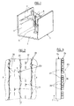
- Figure 1 shows a single dipole 1 secured to the bottom 2 of an antenna housing 3 and surrounded by metal screens 4.
- the dipole is made up of a non-radiating bottom portion 5 and a radiating top portion 6.
- Arrows 7 represent multiple reflections that occur on the screens 4 because of their proximity.
- FIG. 2 A portion of an antenna of the present invention is shown diagrammatically in Figure 2.
- the antenna comprises two arrays 21 forming parallel rows, made up of individual radiating elements 22.
- the arrays 21 are implanted in such a manner that the radiating elements 22 are offset relative to one another.
- the arrays 21 are separated by screens 23 which are parallel thereto along the longitudinal axis Z-Z of the antenna.
- Figure 3 is a side view of a screen 23 looking in the transverse direction X-X of the antenna.
- the bottom portion 24 of the screen 23 is constituted by a plane metal sheet of height that is of the same order as the height of the non-radiating bottom portion of the individual radiating elements 22.
- the screen 23 also has a high portion 25 made up of panels 26 following one another in the longitudinal direction Z-Z.
- Each panel 26 is made up of a central zone 27 extending the bottom portion, and lying between two wings 28.
- the panels 26 are inclined so as to make an angle with the longitudinal axis Z-Z of the antenna, alternating in one direction and in the opposite direction relative to the axis Z-Z, thus forming a substantially zigzag line 29.
- Contiguous screens 23 are installed in such a manner that the concave and convex direction changes of the zigzag line 29 correspond so as to form a deflector around each radiating element 22 as represented by arrows 30 for the purpose of deflecting reflections and thus preventing them from returning to the radiating elements 22.
- an antenna 41 of the invention comprising four arrays 42 of individual radiating elements or dipoles 43 in alignment, forming parallel plane rows disposed perpendicularly to the base 44 of the antenna 41 on which they are secured.
- the dipoles 43 are made on a printed circuit.
- the distance between the arrays 42 is half a wavelength ⁇ , where ⁇ is the wavelength at the center frequency of antenna operation.
- the arrays 42 are implanted so that the dipoles 43 are offset relative to one another by one half-wavelength.
- the arrays 42 are secured to the base 44 of the antenna 41 that has four inlet connectors 45 each corresponding to a respective one of the four arrays 42 of radiating elements 43 as shown.
- Each dipole 43 has a non-radiating bottom portion 46 surmounted by a radiating top portion 47.
- Between the arrays 42 there are placed parallel metal screens 48 presenting total height of substantially the same order as the height of the arrays 42.
- Each screen 48 has a plane bottom portion 49 and a top portion 50 presenting panels 51 extending in a plane different from that of the plane bottom portion 49.
- the plane of the bottom portion 49 is also the mean plane P-P of the screen 48.
- Each panel 51 has a central zone 52 extending the bottom portion 49 and wings 53 cut out on either side of the central zone 52.
- a screen 48 of the invention is shown in an enlarged view in Figures 6 and 7.
- the bottom portion 49 is of a height that corresponds to the height of the non-radiating portions 46 of the facing dipoles 43.
- the top portion 50 extends the bottom portion 49 and faces the radiating portions 47 of the dipoles 43.
- the top portion 50 presents cuts in the form of regularly-spaced vertical slots that are extended on either side by incomplete horizontal cuts leaving between each pair of slots a central zone 52 that remains attached to the bottom portion 49.
- the total length L of a panel 51 lies in the range ⁇ /2 to ⁇ /4.
- Adjacent wings 53 connected to different central zones 52 are folded symmetrically to the same side, such that two successive panels 51 are both oriented in respective different directions symmetrically relative to the mean plane P-P of the screen 48.
- the distance D between two central zones 52 included in panels 51 that are oriented in the same direction lies in the range 0.7 ⁇ and 0.9 ⁇ .
- the wings 53 are preferably of a height h lying in the range ⁇ /7 and ⁇ /11, and of a length d lying in the range ⁇ /7 and ⁇ /11.
Landscapes
- Aerials With Secondary Devices (AREA)
- Variable-Direction Aerials And Aerial Arrays (AREA)
Abstract

Description
- The present invention relates to a telecommunications antenna as used in particular for cellular telephony, such as, for example, an adaptive array system (AAS) for the WiMax application (Worldwide Interoperability for Microwave Access).
- An antenna of this type is made up of closely-spaced arrays of radiating elements obtained by the printed circuit technique. Such an antenna is made up of parallel arrays of dipoles placed in a housing that acts as a reflector. These antennas, often referred to as "patch" antennas, are presently in widespread use because of their very small size, of their manufacturing technology that is extremely simple, and of their cost that is moderate since they are mass-produced.
- Nevertheless, such antennas present difficulties in manufacture because of conflicts that exist between different design criteria. In particular, the mutual coupling that can occur between individual radiating elements when they are close together, even though it can improve the performance of the antenna, nevertheless also presents certain negative effects, such as distorting the spectrum of the antenna or modifying the input impedance of the elements at a given frequency. It is therefore appropriate to limit such coupling without significantly increasing the weight or the size of the antenna.
- In order to preserve uniform radiation, it is necessary to maintain good quality decoupling between the arrays of dipoles. Usually, the arrays of dipoles are generally isolated from one another by simple screen-forming metal walls. In order to obtain better decoupling, one solution is to increase the height of the screen so as to block electromagnetic transmission between the elements. However, when the walls are very close together, the radiating elements become confined in a small space by the screens on which multiple reflections occur, thereby reducing bandwidth. The performance of the antenna, and in particular its standing wave ratio (SWR), is thus degraded which leads to a mismatch between the input impedance of the antenna and the impedance of the transmitter (when transmission is involved). It is associated with the modulus of the reflection coefficient of the antenna.
- To solve this problem, proposals have been made to place radiating elements side by side on a reflector, for example. A conductive metal line placed in the same plane as the elements and connected to ground and to the reflector surrounds these radiating elements. The radiating elements and the metal line can be made in particular by etching a layer of copper that covers a dielectric layer.
- That embodiment is applicable only to elements that are contained completely within a plane parallel to that of the reflector. That solution is not applicable to radiating elements that occupy a plane perpendicular to the reflector, as applies to dipoles. The mechanical structure to be implemented under such circumstances is complex and onerous.
- An object of the present invention is to eliminate the drawbacks of the prior art, and in particular to minimize the reflections that exist between the metal walls and the radiating elements, while conserving a high level of decoupling.
- The present invention provides an antenna comprising at least two arrays comprising respective pluralities of radiating elements in alignment, disposed in parallel planes, and metal screens interposed between the arrays, the antenna being characterized in that each metal screen comprises a bottom portion facing non-radiating portions of the radiating elements and comprising respective plane sheets disposed in planes parallel to the planes of the arrays, and top portions facing the radiating portions of the radiating elements and comprising panels, each forming an angle with the planes of the bottom portions.
- Advantageously, this angle is no greater than 45°, and preferably lies in the
range 25° to 45° so as to deflect reflections, thus preventing them from reaching the dipoles. - The total length of a panel preferably lies in the range λ/2 to λ/4, where λ is the wavelength of the center frequency of antenna operation.
- Each panel is oriented in alternation in one direction and in the other, on either side of the plane of the bottom portion.
- In a preferred embodiment of the invention, each panel comprises two wings connected to a central zone attached to the bottom portion of the screen.
- Preferably, the central zones of two panels oriented in the same direction are separated by a distance lying in the range 0.7λ to 0.9λ.
- Preferably, each wing has a height lying in the range λ/7 to λ/11.
- Also preferably, each wing has a length lying in the range λ/7 to λ/11.
- The present invention also provides a method of manufacturing the above-described antenna. Making a screen comprises the following steps in particular:
- . cutting at least two spaced-apart vertical slots in a fraction of the height of a plane plate;
- . extending the slots horizontally towards each other in incomplete manner so as to retain a central zone attached to the non-cut portion of the plate and form wings on either side of the central zone; and
- . folding the resulting wings on either side of the central zone in alternation in one direction and in the other direction.
- Other characteristics and advantages of the present invention appear on reading the following description of an embodiment, given naturally by way of non-limiting illustration, and from the accompanying drawings, in which:
- . Figure 1 is a diagrammatic view of a radiating element in a confined environment;
- . Figure 2 is a diagrammatic plan view of a portion of the antenna of the invention;
- . Figure 3 is a diagrammatic side view of a screen of the Figure 2 antenna;
- . Figure 4 is a perspective view of an embodiment of an antenna of the invention;
- . Figure 5 is a detailed view of a portion of the Figure 4 antenna;
- . Figure 6 is a fragmentary perspective view of a screen of the Figure 4 antenna; and
- . Figure 7 is a fragmentary plan view of a screen of the Figure 4 antenna.
- Figure 1 shows a single dipole 1 secured to the
bottom 2 of anantenna housing 3 and surrounded bymetal screens 4. The dipole is made up of anon-radiating bottom portion 5 and a radiating top portion 6. Arrows 7 represent multiple reflections that occur on thescreens 4 because of their proximity. - A portion of an antenna of the present invention is shown diagrammatically in Figure 2. The antenna comprises two
arrays 21 forming parallel rows, made up of individualradiating elements 22. In order to reduce coupling, thearrays 21 are implanted in such a manner that theradiating elements 22 are offset relative to one another. Thearrays 21 are separated byscreens 23 which are parallel thereto along the longitudinal axis Z-Z of the antenna. Figure 3 is a side view of ascreen 23 looking in the transverse direction X-X of the antenna. Thebottom portion 24 of thescreen 23 is constituted by a plane metal sheet of height that is of the same order as the height of the non-radiating bottom portion of the individualradiating elements 22. Thescreen 23 also has ahigh portion 25 made up ofpanels 26 following one another in the longitudinal direction Z-Z. Eachpanel 26 is made up of acentral zone 27 extending the bottom portion, and lying between twowings 28. Thepanels 26 are inclined so as to make an angle with the longitudinal axis Z-Z of the antenna, alternating in one direction and in the opposite direction relative to the axis Z-Z, thus forming a substantiallyzigzag line 29.Contiguous screens 23 are installed in such a manner that the concave and convex direction changes of thezigzag line 29 correspond so as to form a deflector around eachradiating element 22 as represented byarrows 30 for the purpose of deflecting reflections and thus preventing them from returning to theradiating elements 22. - In the embodiment shown in Figures 4 and 5, there can be seen an antenna 41 of the invention comprising four
arrays 42 of individual radiating elements ordipoles 43 in alignment, forming parallel plane rows disposed perpendicularly to thebase 44 of the antenna 41 on which they are secured. Thedipoles 43 are made on a printed circuit. For reasons of radio-frequency performance, the distance between thearrays 42 is half a wavelength λ, where λ is the wavelength at the center frequency of antenna operation. In order to reduce coupling, thearrays 42 are implanted so that thedipoles 43 are offset relative to one another by one half-wavelength. Thearrays 42 are secured to thebase 44 of the antenna 41 that has fourinlet connectors 45 each corresponding to a respective one of the fourarrays 42 of radiatingelements 43 as shown. Eachdipole 43 has anon-radiating bottom portion 46 surmounted by a radiatingtop portion 47. Between thearrays 42, there are placedparallel metal screens 48 presenting total height of substantially the same order as the height of thearrays 42. Eachscreen 48 has aplane bottom portion 49 and atop portion 50 presentingpanels 51 extending in a plane different from that of theplane bottom portion 49. The plane of thebottom portion 49 is also the mean plane P-P of thescreen 48. Eachpanel 51 has acentral zone 52 extending thebottom portion 49 andwings 53 cut out on either side of thecentral zone 52. - A
screen 48 of the invention is shown in an enlarged view in Figures 6 and 7. Thebottom portion 49 is of a height that corresponds to the height of thenon-radiating portions 46 of the facingdipoles 43. Thetop portion 50 extends thebottom portion 49 and faces the radiatingportions 47 of thedipoles 43. Thetop portion 50 presents cuts in the form of regularly-spaced vertical slots that are extended on either side by incomplete horizontal cuts leaving between each pair of slots acentral zone 52 that remains attached to thebottom portion 49. On either side of eachcentral zone 52 there are twowings 53, folded towards opposite sides of the mean plane P-P of thescreen 48 containing thecentral zone 52, in such a manner as to form anangle 54 with the mean plane P-P lying in therange 25° to 45°. The total length L of apanel 51 lies in the range λ/2 to λ/4.Adjacent wings 53 connected to differentcentral zones 52 are folded symmetrically to the same side, such that twosuccessive panels 51 are both oriented in respective different directions symmetrically relative to the mean plane P-P of thescreen 48. The distance D between twocentral zones 52 included inpanels 51 that are oriented in the same direction lies in the range 0.7λ and 0.9λ. In the embodiment shown, thewings 53 are preferably of a height h lying in the range λ/7 and λ/11, and of a length d lying in the range λ/7 and λ/11.
Claims (10)
- An antenna comprising at least two arrays (42) comprising respective pluralities of radiating elements (43) in alignment, disposed in parallel planes, and metal screens (48) interposed between the arrays (42), the antenna being characterized in that each metal screen (48) comprises a bottom portion (49) facing non-radiating portions (46) of the radiating elements (43) and comprising respective plane sheets disposed in planes parallel to the planes of the arrays (42), and top portions (50) facing the radiating portions (47) of the radiating elements (43) and comprising panels (51), each forming an angle with the planes of the bottom portions (49).
- An antenna according to claim 1, in which the angle is not greater than 45°.
- An antenna according to claim 2, in which the angle lies in the range 25° to 45°.
- An antenna according to any preceding claim, in which the total length of a panel lies in the range λ/2 to λ/4.
- An antenna according to any preceding claim, in which each panel is oriented in alternation in one direction and in another direction on either side of the plane of the bottom portion.
- An antenna according to any preceding claim, in which each panel (51) comprises two wings (53) connected to a central zone (52) attached to the bottom portion (49) of the screen (48).
- An antenna according to claim 6, in which the central zones of two panels there are both oriented in the same direction are spaced apart by a distance lying in the range 0.7λ and 0.9λ.
- An antenna according to claim 6 or claim 7, in which each wing has a height lying in the range λ/7 to λ/11.
- An antenna according to any one of claims 6 to 8, in which each wing has a length lying in the range λ/7 to λ/11.
- A method of fabricating an antenna according to any preceding claim, characterized in that making the screen comprises the following steps:. cutting at least two spaced-apart vertical slots in a fraction of the height of a plane plate;. extending the slots horizontally towards each other in incomplete manner so as to retain a central zone attached to the non-cut portion of the plate and form wings on either side of the central zone; and. folding the resulting wings on either side of the central zone in alternation in one direction and in the other direction.
Applications Claiming Priority (1)
| Application Number | Priority Date | Filing Date | Title |
|---|---|---|---|
| FR0654288A FR2907264A1 (en) | 2006-10-16 | 2006-10-16 | DECOUPLING NETWORKS OF RADIANT ELEMENTS OF AN ANTENNA |
Publications (1)
| Publication Number | Publication Date |
|---|---|
| EP1914833A1 true EP1914833A1 (en) | 2008-04-23 |
Family
ID=38162132
Family Applications (1)
| Application Number | Title | Priority Date | Filing Date |
|---|---|---|---|
| EP07117631A Withdrawn EP1914833A1 (en) | 2006-10-16 | 2007-10-01 | Decoupling arrays of radiating elements of an antenna |
Country Status (6)
| Country | Link |
|---|---|
| US (1) | US7592965B2 (en) |
| EP (1) | EP1914833A1 (en) |
| KR (1) | KR20090078802A (en) |
| CN (1) | CN101165969A (en) |
| FR (1) | FR2907264A1 (en) |
| WO (1) | WO2008046730A1 (en) |
Cited By (1)
| Publication number | Priority date | Publication date | Assignee | Title |
|---|---|---|---|---|
| CN108028462A (en) * | 2015-11-25 | 2018-05-11 | 康普技术有限责任公司 | Phased Array Antenna with Decoupling Element |
Families Citing this family (4)
| Publication number | Priority date | Publication date | Assignee | Title |
|---|---|---|---|---|
| US20140111396A1 (en) * | 2012-10-19 | 2014-04-24 | Futurewei Technologies, Inc. | Dual Band Interleaved Phased Array Antenna |
| KR102412521B1 (en) * | 2018-01-12 | 2022-06-23 | 주식회사 케이엠더블유 | Antenna Apparatus |
| WO2020094219A1 (en) * | 2018-11-07 | 2020-05-14 | Huawei Technologies Co., Ltd. | Antenna and base station |
| WO2020190863A1 (en) | 2019-03-21 | 2020-09-24 | Commscope Technologies Llc | Base station antennas having parasitic assemblies for improving cross-polarization discrimination performance |
Citations (2)
| Publication number | Priority date | Publication date | Assignee | Title |
|---|---|---|---|---|
| GB2338346A (en) * | 1998-06-09 | 1999-12-15 | Samsung Electronics Co Ltd | Wide-band micropstrip dipole antenna array |
| US6023244A (en) * | 1997-02-14 | 2000-02-08 | Telefonaktiebolaget Lm Ericsson | Microstrip antenna having a metal frame for control of an antenna lobe |
-
2006
- 2006-10-16 FR FR0654288A patent/FR2907264A1/en not_active Withdrawn
-
2007
- 2007-10-01 EP EP07117631A patent/EP1914833A1/en not_active Withdrawn
- 2007-10-01 WO PCT/EP2007/060364 patent/WO2008046730A1/en not_active Ceased
- 2007-10-01 KR KR1020097007783A patent/KR20090078802A/en not_active Abandoned
- 2007-10-15 US US11/872,131 patent/US7592965B2/en not_active Expired - Fee Related
- 2007-10-16 CN CNA2007101625132A patent/CN101165969A/en active Pending
Patent Citations (2)
| Publication number | Priority date | Publication date | Assignee | Title |
|---|---|---|---|---|
| US6023244A (en) * | 1997-02-14 | 2000-02-08 | Telefonaktiebolaget Lm Ericsson | Microstrip antenna having a metal frame for control of an antenna lobe |
| GB2338346A (en) * | 1998-06-09 | 1999-12-15 | Samsung Electronics Co Ltd | Wide-band micropstrip dipole antenna array |
Non-Patent Citations (1)
| Title |
|---|
| MAILLOUX R J: "REDUCTION OF MUTUAL COUPLING USING PERFECTLY CONDUCTING FENCES", IEEE TRANSACTIONS ON ANTENNAS AND PROPAGATION, IEEE SERVICE CENTER, PISCATAWAY, NJ, US, vol. 19, no. 2, March 1971 (1971-03-01), pages 166 - 173, XP002094413, ISSN: 0018-926X * |
Cited By (1)
| Publication number | Priority date | Publication date | Assignee | Title |
|---|---|---|---|---|
| CN108028462A (en) * | 2015-11-25 | 2018-05-11 | 康普技术有限责任公司 | Phased Array Antenna with Decoupling Element |
Also Published As
| Publication number | Publication date |
|---|---|
| KR20090078802A (en) | 2009-07-20 |
| WO2008046730A1 (en) | 2008-04-24 |
| CN101165969A (en) | 2008-04-23 |
| FR2907264A1 (en) | 2008-04-18 |
| US20080094286A1 (en) | 2008-04-24 |
| US7592965B2 (en) | 2009-09-22 |
Similar Documents
| Publication | Publication Date | Title |
|---|---|---|
| US10840593B1 (en) | Antenna devices to suppress ground plane interference | |
| EP3096402B1 (en) | Antenna device, wireless communication apparatus, and radar apparatus | |
| US7446712B2 (en) | Composite right/left-handed transmission line based compact resonant antenna for RF module integration | |
| JP6820135B2 (en) | Ultra-wideband antenna elements and arrays with low cross-polarization decade bandwidth | |
| US10587047B2 (en) | Dual-band filtering antenna array using filtering antenna elements for mutual coupling suppression | |
| EP2826097B1 (en) | Phased array antenna | |
| US7221322B1 (en) | Dual polarization antenna array with inter-element coupling and associated methods | |
| WO2017161611A1 (en) | Multi-band single feed dielectric resonator antenna (dra) array | |
| US20100007572A1 (en) | Dual-polarized phased array antenna with vertical features to eliminate scan blindness | |
| EP1777780A2 (en) | Enhanced bandwidth single layer current sheet antenna | |
| EP1775795A1 (en) | Broadband proximity-coupled cavity backed patch antenna | |
| US20210159609A1 (en) | Capacitive-coupled comb-line microstrip array antenna | |
| US7532170B1 (en) | Conformal end-fire arrays on high impedance ground plane | |
| US8736514B2 (en) | Antenna | |
| US7592965B2 (en) | Decoupling arrays of radiating elements of an antenna | |
| US4912482A (en) | Antenna | |
| CA2570647C (en) | Single polarization slot antenna array with inter-element coupling and associated methods | |
| US7408519B2 (en) | Dual polarization antenna array with inter-element capacitive coupling plate and associated methods | |
| EP1798817A1 (en) | Single polarization slot antenna array with inter-element capacitive coupling plate and associated methods | |
| US12586925B2 (en) | Antennas with periodic structures | |
| CN113517560B (en) | Millimeter wave array antenna capable of scanning at wide angle | |
| US7573434B2 (en) | Decoupling arrays for radiating elements of an antenna | |
| EP3528340B1 (en) | Antennas | |
| KR102901634B1 (en) | Planar broadband array antenna using adl structures | |
| CN110797638A (en) | A Low Profile Millimeter Wave Printed Board Antenna Array |
Legal Events
| Date | Code | Title | Description |
|---|---|---|---|
| PUAI | Public reference made under article 153(3) epc to a published international application that has entered the european phase |
Free format text: ORIGINAL CODE: 0009012 |
|
| AK | Designated contracting states |
Kind code of ref document: A1 Designated state(s): AT BE BG CH CY CZ DE DK EE ES FI FR GB GR HU IE IS IT LI LT LU LV MC MT NL PL PT RO SE SI SK TR |
|
| AX | Request for extension of the european patent |
Extension state: AL BA HR MK RS |
|
| 17P | Request for examination filed |
Effective date: 20081023 |
|
| AKX | Designation fees paid |
Designated state(s): AT BE BG CH CY CZ DE DK EE ES FI FR GB GR HU IE IS IT LI LT LU LV MC MT NL PL PT RO SE SI SK TR |
|
| GRAP | Despatch of communication of intention to grant a patent |
Free format text: ORIGINAL CODE: EPIDOSNIGR1 |
|
| GRAS | Grant fee paid |
Free format text: ORIGINAL CODE: EPIDOSNIGR3 |
|
| STAA | Information on the status of an ep patent application or granted ep patent |
Free format text: STATUS: THE APPLICATION IS DEEMED TO BE WITHDRAWN |
|
| 18D | Application deemed to be withdrawn |
Effective date: 20091013 |