EP1911102B1 - Method for passivating a substrate surface - Google Patents
Method for passivating a substrate surface Download PDFInfo
- Publication number
- EP1911102B1 EP1911102B1 EP06783861A EP06783861A EP1911102B1 EP 1911102 B1 EP1911102 B1 EP 1911102B1 EP 06783861 A EP06783861 A EP 06783861A EP 06783861 A EP06783861 A EP 06783861A EP 1911102 B1 EP1911102 B1 EP 1911102B1
- Authority
- EP
- European Patent Office
- Prior art keywords
- plasma
- substrate
- layer
- sio
- process chamber
- Prior art date
- Legal status (The legal status is an assumption and is not a legal conclusion. Google has not performed a legal analysis and makes no representation as to the accuracy of the status listed.)
- Expired - Lifetime
Links
Images
Classifications
-
- H—ELECTRICITY
- H10—SEMICONDUCTOR DEVICES; ELECTRIC SOLID-STATE DEVICES NOT OTHERWISE PROVIDED FOR
- H10P—GENERIC PROCESSES OR APPARATUS FOR THE MANUFACTURE OR TREATMENT OF DEVICES COVERED BY CLASS H10
- H10P14/00—Formation of materials, e.g. in the shape of layers or pillars
- H10P14/60—Formation of materials, e.g. in the shape of layers or pillars of insulating materials
- H10P14/63—Formation of materials, e.g. in the shape of layers or pillars of insulating materials characterised by the formation processes
- H10P14/6326—Deposition processes
- H10P14/6328—Deposition from the gas or vapour phase
- H10P14/6334—Deposition from the gas or vapour phase using decomposition or reaction of gaseous or vapour phase compounds, i.e. chemical vapour deposition
- H10P14/6336—Deposition from the gas or vapour phase using decomposition or reaction of gaseous or vapour phase compounds, i.e. chemical vapour deposition in the presence of a plasma [PECVD]
-
- C—CHEMISTRY; METALLURGY
- C23—COATING METALLIC MATERIAL; COATING MATERIAL WITH METALLIC MATERIAL; CHEMICAL SURFACE TREATMENT; DIFFUSION TREATMENT OF METALLIC MATERIAL; COATING BY VACUUM EVAPORATION, BY SPUTTERING, BY ION IMPLANTATION OR BY CHEMICAL VAPOUR DEPOSITION, IN GENERAL; INHIBITING CORROSION OF METALLIC MATERIAL OR INCRUSTATION IN GENERAL
- C23C—COATING METALLIC MATERIAL; COATING MATERIAL WITH METALLIC MATERIAL; SURFACE TREATMENT OF METALLIC MATERIAL BY DIFFUSION INTO THE SURFACE, BY CHEMICAL CONVERSION OR SUBSTITUTION; COATING BY VACUUM EVAPORATION, BY SPUTTERING, BY ION IMPLANTATION OR BY CHEMICAL VAPOUR DEPOSITION, IN GENERAL
- C23C16/00—Chemical coating by decomposition of gaseous compounds, without leaving reaction products of surface material in the coating, i.e. chemical vapour deposition [CVD] processes
- C23C16/22—Chemical coating by decomposition of gaseous compounds, without leaving reaction products of surface material in the coating, i.e. chemical vapour deposition [CVD] processes characterised by the deposition of inorganic material, other than metallic material
- C23C16/30—Deposition of compounds, mixtures or solid solutions, e.g. borides, carbides, nitrides
- C23C16/40—Oxides
- C23C16/401—Oxides containing silicon
- C23C16/402—Silicon dioxide
-
- C—CHEMISTRY; METALLURGY
- C23—COATING METALLIC MATERIAL; COATING MATERIAL WITH METALLIC MATERIAL; CHEMICAL SURFACE TREATMENT; DIFFUSION TREATMENT OF METALLIC MATERIAL; COATING BY VACUUM EVAPORATION, BY SPUTTERING, BY ION IMPLANTATION OR BY CHEMICAL VAPOUR DEPOSITION, IN GENERAL; INHIBITING CORROSION OF METALLIC MATERIAL OR INCRUSTATION IN GENERAL
- C23C—COATING METALLIC MATERIAL; COATING MATERIAL WITH METALLIC MATERIAL; SURFACE TREATMENT OF METALLIC MATERIAL BY DIFFUSION INTO THE SURFACE, BY CHEMICAL CONVERSION OR SUBSTITUTION; COATING BY VACUUM EVAPORATION, BY SPUTTERING, BY ION IMPLANTATION OR BY CHEMICAL VAPOUR DEPOSITION, IN GENERAL
- C23C16/00—Chemical coating by decomposition of gaseous compounds, without leaving reaction products of surface material in the coating, i.e. chemical vapour deposition [CVD] processes
- C23C16/44—Chemical coating by decomposition of gaseous compounds, without leaving reaction products of surface material in the coating, i.e. chemical vapour deposition [CVD] processes characterised by the method of coating
- C23C16/50—Chemical coating by decomposition of gaseous compounds, without leaving reaction products of surface material in the coating, i.e. chemical vapour deposition [CVD] processes characterised by the method of coating using electric discharges
- C23C16/513—Chemical coating by decomposition of gaseous compounds, without leaving reaction products of surface material in the coating, i.e. chemical vapour deposition [CVD] processes characterised by the method of coating using electric discharges using plasma jets
-
- C—CHEMISTRY; METALLURGY
- C23—COATING METALLIC MATERIAL; COATING MATERIAL WITH METALLIC MATERIAL; CHEMICAL SURFACE TREATMENT; DIFFUSION TREATMENT OF METALLIC MATERIAL; COATING BY VACUUM EVAPORATION, BY SPUTTERING, BY ION IMPLANTATION OR BY CHEMICAL VAPOUR DEPOSITION, IN GENERAL; INHIBITING CORROSION OF METALLIC MATERIAL OR INCRUSTATION IN GENERAL
- C23C—COATING METALLIC MATERIAL; COATING MATERIAL WITH METALLIC MATERIAL; SURFACE TREATMENT OF METALLIC MATERIAL BY DIFFUSION INTO THE SURFACE, BY CHEMICAL CONVERSION OR SUBSTITUTION; COATING BY VACUUM EVAPORATION, BY SPUTTERING, BY ION IMPLANTATION OR BY CHEMICAL VAPOUR DEPOSITION, IN GENERAL
- C23C16/00—Chemical coating by decomposition of gaseous compounds, without leaving reaction products of surface material in the coating, i.e. chemical vapour deposition [CVD] processes
- C23C16/56—After-treatment
-
- H—ELECTRICITY
- H10—SEMICONDUCTOR DEVICES; ELECTRIC SOLID-STATE DEVICES NOT OTHERWISE PROVIDED FOR
- H10F—INORGANIC SEMICONDUCTOR DEVICES SENSITIVE TO INFRARED RADIATION, LIGHT, ELECTROMAGNETIC RADIATION OF SHORTER WAVELENGTH OR CORPUSCULAR RADIATION
- H10F71/00—Manufacture or treatment of devices covered by this subclass
- H10F71/129—Passivating
-
- H—ELECTRICITY
- H10—SEMICONDUCTOR DEVICES; ELECTRIC SOLID-STATE DEVICES NOT OTHERWISE PROVIDED FOR
- H10P—GENERIC PROCESSES OR APPARATUS FOR THE MANUFACTURE OR TREATMENT OF DEVICES COVERED BY CLASS H10
- H10P14/00—Formation of materials, e.g. in the shape of layers or pillars
- H10P14/60—Formation of materials, e.g. in the shape of layers or pillars of insulating materials
- H10P14/66—Formation of materials, e.g. in the shape of layers or pillars of insulating materials characterised by the type of materials
- H10P14/662—Laminate layers, e.g. stacks of alternating high-k metal oxides
-
- H—ELECTRICITY
- H10—SEMICONDUCTOR DEVICES; ELECTRIC SOLID-STATE DEVICES NOT OTHERWISE PROVIDED FOR
- H10P—GENERIC PROCESSES OR APPARATUS FOR THE MANUFACTURE OR TREATMENT OF DEVICES COVERED BY CLASS H10
- H10P14/00—Formation of materials, e.g. in the shape of layers or pillars
- H10P14/60—Formation of materials, e.g. in the shape of layers or pillars of insulating materials
- H10P14/66—Formation of materials, e.g. in the shape of layers or pillars of insulating materials characterised by the type of materials
- H10P14/668—Formation of materials, e.g. in the shape of layers or pillars of insulating materials characterised by the type of materials the materials being characterised by the deposition precursor materials
- H10P14/6681—Formation of materials, e.g. in the shape of layers or pillars of insulating materials characterised by the type of materials the materials being characterised by the deposition precursor materials the precursor containing a compound comprising Si
- H10P14/6684—Formation of materials, e.g. in the shape of layers or pillars of insulating materials characterised by the type of materials the materials being characterised by the deposition precursor materials the precursor containing a compound comprising Si the compound comprising silicon and oxygen
- H10P14/6686—Formation of materials, e.g. in the shape of layers or pillars of insulating materials characterised by the type of materials the materials being characterised by the deposition precursor materials the precursor containing a compound comprising Si the compound comprising silicon and oxygen the compound being a molecule comprising at least one silicon-oxygen bond and the compound having hydrogen or an organic group attached to the silicon or oxygen, e.g. a siloxane
-
- H—ELECTRICITY
- H10—SEMICONDUCTOR DEVICES; ELECTRIC SOLID-STATE DEVICES NOT OTHERWISE PROVIDED FOR
- H10P—GENERIC PROCESSES OR APPARATUS FOR THE MANUFACTURE OR TREATMENT OF DEVICES COVERED BY CLASS H10
- H10P14/00—Formation of materials, e.g. in the shape of layers or pillars
- H10P14/60—Formation of materials, e.g. in the shape of layers or pillars of insulating materials
- H10P14/69—Inorganic materials
- H10P14/694—Inorganic materials composed of nitrides
- H10P14/6943—Inorganic materials composed of nitrides containing silicon
- H10P14/69433—Inorganic materials composed of nitrides containing silicon the material being a silicon nitride not containing oxygen, e.g. SixNy or SixByNz
-
- H—ELECTRICITY
- H10—SEMICONDUCTOR DEVICES; ELECTRIC SOLID-STATE DEVICES NOT OTHERWISE PROVIDED FOR
- H10P—GENERIC PROCESSES OR APPARATUS FOR THE MANUFACTURE OR TREATMENT OF DEVICES COVERED BY CLASS H10
- H10P95/00—Generic processes or apparatus for manufacture or treatments not covered by the other groups of this subclass
-
- H—ELECTRICITY
- H10—SEMICONDUCTOR DEVICES; ELECTRIC SOLID-STATE DEVICES NOT OTHERWISE PROVIDED FOR
- H10P—GENERIC PROCESSES OR APPARATUS FOR THE MANUFACTURE OR TREATMENT OF DEVICES COVERED BY CLASS H10
- H10P14/00—Formation of materials, e.g. in the shape of layers or pillars
- H10P14/60—Formation of materials, e.g. in the shape of layers or pillars of insulating materials
- H10P14/66—Formation of materials, e.g. in the shape of layers or pillars of insulating materials characterised by the type of materials
- H10P14/668—Formation of materials, e.g. in the shape of layers or pillars of insulating materials characterised by the type of materials the materials being characterised by the deposition precursor materials
- H10P14/6681—Formation of materials, e.g. in the shape of layers or pillars of insulating materials characterised by the type of materials the materials being characterised by the deposition precursor materials the precursor containing a compound comprising Si
- H10P14/6682—Formation of materials, e.g. in the shape of layers or pillars of insulating materials characterised by the type of materials the materials being characterised by the deposition precursor materials the precursor containing a compound comprising Si the compound being a silane, e.g. disilane, methylsilane or chlorosilane
-
- H—ELECTRICITY
- H10—SEMICONDUCTOR DEVICES; ELECTRIC SOLID-STATE DEVICES NOT OTHERWISE PROVIDED FOR
- H10P—GENERIC PROCESSES OR APPARATUS FOR THE MANUFACTURE OR TREATMENT OF DEVICES COVERED BY CLASS H10
- H10P14/00—Formation of materials, e.g. in the shape of layers or pillars
- H10P14/60—Formation of materials, e.g. in the shape of layers or pillars of insulating materials
- H10P14/69—Inorganic materials
- H10P14/692—Inorganic materials composed of oxides, glassy oxides or oxide-based glasses
- H10P14/6921—Inorganic materials composed of oxides, glassy oxides or oxide-based glasses containing silicon
- H10P14/69215—Inorganic materials composed of oxides, glassy oxides or oxide-based glasses containing silicon the material being a silicon oxide, e.g. SiO2
-
- Y—GENERAL TAGGING OF NEW TECHNOLOGICAL DEVELOPMENTS; GENERAL TAGGING OF CROSS-SECTIONAL TECHNOLOGIES SPANNING OVER SEVERAL SECTIONS OF THE IPC; TECHNICAL SUBJECTS COVERED BY FORMER USPC CROSS-REFERENCE ART COLLECTIONS [XRACs] AND DIGESTS
- Y02—TECHNOLOGIES OR APPLICATIONS FOR MITIGATION OR ADAPTATION AGAINST CLIMATE CHANGE
- Y02E—REDUCTION OF GREENHOUSE GAS [GHG] EMISSIONS, RELATED TO ENERGY GENERATION, TRANSMISSION OR DISTRIBUTION
- Y02E10/00—Energy generation through renewable energy sources
- Y02E10/50—Photovoltaic [PV] energy
-
- Y—GENERAL TAGGING OF NEW TECHNOLOGICAL DEVELOPMENTS; GENERAL TAGGING OF CROSS-SECTIONAL TECHNOLOGIES SPANNING OVER SEVERAL SECTIONS OF THE IPC; TECHNICAL SUBJECTS COVERED BY FORMER USPC CROSS-REFERENCE ART COLLECTIONS [XRACs] AND DIGESTS
- Y02—TECHNOLOGIES OR APPLICATIONS FOR MITIGATION OR ADAPTATION AGAINST CLIMATE CHANGE
- Y02P—CLIMATE CHANGE MITIGATION TECHNOLOGIES IN THE PRODUCTION OR PROCESSING OF GOODS
- Y02P70/00—Climate change mitigation technologies in the production process for final industrial or consumer products
- Y02P70/50—Manufacturing or production processes characterised by the final manufactured product
Definitions
- the invention relates to a method for passivating at least a part of a surface of a semiconductor substrate.
- Such a method is known from practice.
- a substrate surface of a semiconductor substrate is passivated by realizing a SiO x layer, for instance a layer of silicon oxide, on that surface.
- a SiO x layer for instance a layer of silicon oxide
- Another known method comprises sputtering the SiO x layer.
- SSV surface recombination velocity
- low temperature surface passivation for silicon solar cells discloses a low temperature surface passivation for silicon solar cells.
- the method involves PECVD as a method to achieve surface passivation at low temperatures.
- Publication US-A-5 462 898 discloses a method for passivating silicon devices at low temperature, involving PECVD as well.
- the present invention contemplates obviating above-mentioned drawbacks of the known method.
- the invention contemplates a method for passivating a semiconductor substrate, in which a SiO x layer obtained with the method has a relatively low surface recombination velocity, while the substrate particularly has a relatively low resistivity.
- the method according to the invention is characterized by the features of claim 1 and of claim 2.
- the anneal treatment comprises a temperature treatment in a gas environment, the temperature treatment including maintaining the SiO x layer at a treatment temperature in the range of 250°C-1000°C.
- At least above-mentioned SiO x layer realized on the substrate is maintained at a treatment temperature which is higher than 350°C. It is found that, with such a temperature treatment, particularly good results can be obtained.
- the treatment temperature is in the range of 250°C-1000°C, in particular in the range of 500°C-700°C, more in particular in the range of 550°C-650°C.
- the temperature treatment may, for instance, take less than 20 min.
- the substrate may, for instance, be cooled, optionally in a forced manner.
- a gas flow is supplied to above-mentioned substrate or at least the SiO x layer realized and the substrate during above-mentioned temperature treatment, to provide above-mentioned gas environment.
- the temperature treatment may, for instance, comprise a forming gas anneal treatment.
- the gas environment may, for instance, be provided by supplying a mixture of nitrogen and hydrogen to the substrate and/or the at least one layer realized on the substrate. In that case, the gas environment may, for instance, comprise a hydrogen-nitrogen environment.
- the gas environment may, for instance, substantially comprise hydrogen gas, for instance by supplying a hydrogen gas flow to the substrate and/or the at least one layer realized on the substrate.
- the gas or gas mixture then preferably has the same above-mentioned substrate treatment temperature.
- H 2 or a mixture of H 2 with an inert gas, for instance N 2 or Ar is supplied to above-mentioned plasma, in particular for annealing the at least one layer and/or for increasing the diffusion of H 2 in the at least one layer.
- an inert gas for instance N 2 or Ar
- a solar cell which is provided with at least a part of a substrate at least obtained with a method according to the invention, can use improved properties in an advantageous manner, for instance a relatively low surface recombination velocity of the substrate surface, which is favorable to the performance of the solar cell.
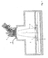
- Figs. 1 and 2 show an apparatus with which at least a deposition or realization of at least one SiO x layer, and for instance one or more other layers on a substrate can be carried out, in a method according to the invention.
- the apparatus is, for instance, well suitable for use in an inline process.
- the apparatus shown in Figs. 1 and 2 is provided with a process chamber 5 on which a DC (direct current) plasma cascade source 3 is provided. Alternatively, a different type of plasma source may be used.
- the DC plasma cascade source 3 of the exemplary embodiment is arranged for generating a plasma with DC voltage.
- the apparatus is provided with a substrate holder 8 for holding one substrate 1 opposite an outflow opening 4 of the plasma source 3 in the process chamber 5.
- the apparatus further comprises heating means (not shown) for heating the substrate 1 during the treatment.
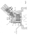
- the plasma cascade source 3 is provided with a cathode 10 located in a front chamber 11 and an anode 12 located at a side of the source 3 proximal to the process chamber 5.
- the front chamber 11 opens into the process chamber 5 via a relatively narrow channel 13 and the above-mentioned plasma outflow opening 4.
- the apparatus is, for instance, dimensioned such that the distance L between the substrate 1 and the plasma outflow opening 4 is approximately 200 mm - 300 mm.
- the channel 13 can be bounded by mutually electrically insulated cascade plates 14 and the above-mentioned anode 12.
- the process chamber 5 is kept at a relatively low pressure, lower than 5000 Pa, and preferably lower than 500 Pa.
- the treatment pressure and the dimensions of the process chamber need to be such that the growth process can still take place.
- the treatment pressure is found to be at least approximately 0.1 mbar for this purpose.
- the pumping means needed to obtain the above-mentioned treatment pressure are not shown in the drawing.
- a plasma is generated during use, for instance by ignition of an inert gas, such as argon, which is present therebetween.
- the pressure in the front chamber 11 is higher than the pressure in the process chamber 5.
- This pressure can, for instance, be substantially atmospheric and be in the range of 0.5-1.5 bar. Because the pressure in the process chamber 5 is considerably lower than the pressure in the front chamber 11, a part of the generated plasma P expands such that it extends via the relatively narrow channel 7 from the above-mentioned outflow opening 4 into the process chamber 5 for contacting the surface of the substrate 1.
- the expanding plasma part may, for instance, reach a supersonic velocity.
- the apparatus is particularly provided with supply means 6, 7 for supplying flows of suitable treatment fluids to the plasma P in, for instance, the anode plate 12 of the source 3 and/or in the process chamber 5.
- supply means may in themselves be designed in different manners, which will be clear to a skilled person.
- the supply means comprise, for instance, an injector 6 designed for introducing one or more treatment fluids into the plasma P near the plasma source 3.
- the supply means further comprise, for instance, a shower head 7 for supplying one or more treatment fluids to the plasma P downstream of the above-mentioned plasma outflow opening 4 near the substrate 1.
- a shower head 7 is, for instance, arranged near or below the plasma source 3 in the process chamber 5.
- the apparatus is provided with sources (not shown) which are connected to the above-mentioned supply means 6, 7 via flow control means, for supplying specific desired treatment fluids thereto.
- sources such as silane, hydrogen and/or oxygen
- no reactive gases such as silane, hydrogen and/or oxygen, are supplied to the plasma in the plasma source 3, so that the source 3 cannot be affected by such gases.
- the cascade source 3 For the purpose of passivating the substrate 1, during use, the cascade source 3 generates a plasma P in the described manner, such that the plasma P contacts the substrate surface of the substrate 1.
- Flows of treatment fluids suitable for SiO x deposition are supplied to the plasma P in a suitable ratio via the supply means 6, 7.
- the process parameters of the plasma treatment process, at least the above-mentioned process chamber pressure, the substrate temperature, the distance L between the plasma source 3 and the substrate 1, and the flow rates of the treatment fluids are preferably such that the apparatus deposits the SiO x layer on the substrate 1 at an advantageous velocity which is, for instance, in the range of 1-15 nm/s, which, for instance, depends on the velocity of the apparatus.
- the above-mentioned substrate temperature, at least during the deposition of SiOx, may, for instance, be in the range of 250-550°C, more in particular in the range of 380-420°C.
- Above-mentioned treatment fluids may comprise various precursors suitable for SiOx deposition.
- D4 and O 2 can be supplied to above-mentioned part of the plasma P, for depositing a SiO x layer on the substrate surface, which is found to yield good results.
- the D4 also known as octamethyltetrasiloxane
- the O 2 may, for instance, be gaseous and be supplied to the plasma via above-mentioned injector 6.
- At least one precursor may, for instance, be selected from the group consisting of: SiH 4 , O 2 , NO 2 , CH 3 SiH 3 (1MS), 2(CH 3 )SiH 2 (2MS), 3(CH 3 )SiH (3MS), siloxanes, hexamethylsiloxane, octamethyltrisiloxane (OMTS), bis(trimethylsiloxy)methylsilane (BTMS), octamethyltetrasiloxane (OMCTS, D4) and TEOS.
- the precursor may further comprise one or more other substances suitable for SiO x .
- the SiO x layer can simply be grown at a constant growth rate, substantially without adjustment during deposition. This is advantageous compared to use of a plasma source driven with AC. Further, with a DC plasma cascade source, a relatively high growth rate can be obtained. It is found that, with this apparatus, a particularly good surface-passivated substrate can be obtained, in particular with a SiO x layer, with a relatively low substrate resistivity.
- a SiN x may be provided, which may, for instance, form an anti-reflection coating. Further, such a SiN x layer may, for instance, supply hydrogen to the deposited SiO x layer for the purpose of passivation of the substrate.
- the SiO x layer and SiN x layer are successively deposited on the substrate 1 by the same deposition apparatus.
- precursors suitable for SiN x deposition for instance NH 3 , SiH 4 , N 2 , and/or other precursors
- precursors suitable for SiN x deposition can be supplied to the plasma P via above-mentioned supply means 6, 7 after deposition of the SiO x , layer.
- the layer stack comprising at least one SiO x layer and at least one SiN x layer is also called a SiO x /SiN x stack.
- the thickness of above-mentioned SiN x layer is preferably in the range of 25 to 100 nm, and may, for instance, be 80 nm.
- an apparatus may be provided for subjecting the substrate to a temperature treatment after deposition of one or more of above-mentioned layers, for instance to a forming gas anneal treatment in which suitable gases are supplied to the substrate.
- the temperature treatment can be carried out in a gas environment, at least such that at least one surface of the at least one layer realized on the substrate is contacted with those gases.
- a gas mixture suitable for the temperature treatment is, for instance, a hydrogen-nitrogen mixture.
- Such a temperature treatment may, for instance, be carried out in a separate thermal treatment apparatus, a separate forming gas anneal apparatus, or the like.
- H 2 or a mixture of H 2 and an inert gas such as N 2 or Ar may be supplied to a plasma P, after the at least one layer has been realized on the substrate, for instance for increasing the diffusion of H 2 in the SiO x layer or the SiO x /SiN x stack.
- a plasma treatment may, for instance, be carried out instead of the above-mentioned temperature treatment or in combination with such a temperature treatment.
- a silicon oxide (SiO) layer was deposited on a substrate surface of a monocrystalline silicon with a method according to the invention, using an above-described apparatus shown in the Figures.
- the layer thickness was approximately 100 nm.
- the substrate inherently had a relatively low resistivity, for instance a resistivity of less than approximately 10 ⁇ cm.
- use was made of an n-doped silicon wafer with a resistivity of 1.4 ⁇ cm.
- the deposited silicon oxide layer was optionally provided with a SiN x layer, using N 2 H 3 and SiH 4 , for forming a SiO x /SiN x stack on the substrate.
- the SiN x layer may, for instance, supply hydrogen to the deposited SiO x layer, and also serve as an anti-reflection layer.
- the substrate was subjected to a temperature treatment, for instance using a suitable forming gas anneal apparatus.
- a temperature treatment for instance using a suitable forming gas anneal apparatus.
- the deposited SiO x layer and/or SiN x layer was maintained at a treatment temperature of approximately 600°C for a treatment period of approximately 15 min, and in particular at an atmospheric pressure.
- a 90% N 2 - 10% H 2 gas mixture was supplied to a surface of the SiO x layer and/or the SiO x /SiN x stack for obtaining a forming gas anneal.
- the substrate and the at least one layer provided thereon were cooled.
- the SiO x layer or SiO x /SiN 2 stack thus obtained was found to have a stable, particularly low surface recombination velocity of approximately 50 cm/s. Therefore, the substrate treated in this manner, which has a very low resistivity, is particularly well suitable for use as, for instance, a 'building block' of solar cells.
- substrates of various semiconductor materials can be used to be passivated by the method according to the invention.
- the method may, for instance, be carried out using more than one plasma source mounted on a process chamber.
- the substrate may, for instance, be loaded into the process chamber 5 from a vacuum environment, such as a load lock brought to a vacuum and mounted to the process chamber. In that case, the pressure in the process chamber 5 can maintain a desired low value during loading.
- the substrate may, for instance, be introduced into the process chamber 5 when that chamber 5 is at an atmospheric pressure, while the chamber 5 is then closed and pumped to the desired pressure by the pumping means.
- the plasma source may, for instance, generate a plasma which exclusively contains argon.
- one or more layers can be applied to the substrate, for instance one or more SiO x layers and one or more optional other layers such as for instance SiN x layers.
- a whole surface of a substrate is passivated by means of a method according to the invention.
- a part of the surface may be passivated by means of the method.
- the thickness of the SiO x layer realized on the substrate by means of the plasma treatment process may, for instance, be in the range of 10-1000 nm.
- a plasma with O 2 as a precursor may, for instance, modify a substrate surface of the substrate, or part of the surface, into SiO x , so that above-mentioned SiO x layer is realized.
- the SiO x layer is, in particular, not realized by means of deposition, but by means of modification.
- the SiO x layer may also be realized in a different manner, however still according to the terms of claims 1 ou 2.
Landscapes
- Chemical & Material Sciences (AREA)
- Engineering & Computer Science (AREA)
- Mechanical Engineering (AREA)
- Chemical Kinetics & Catalysis (AREA)
- General Chemical & Material Sciences (AREA)
- Materials Engineering (AREA)
- Metallurgy (AREA)
- Organic Chemistry (AREA)
- Physics & Mathematics (AREA)
- Plasma & Fusion (AREA)
- Inorganic Chemistry (AREA)
- Chemical Vapour Deposition (AREA)
- Formation Of Insulating Films (AREA)
- Drying Of Semiconductors (AREA)
- Photovoltaic Devices (AREA)
Description
- The invention relates to a method for passivating at least a part of a surface of a semiconductor substrate.
- Such a method is known from practice. In the known method, a substrate surface of a semiconductor substrate is passivated by realizing a SiOx layer, for instance a layer of silicon oxide, on that surface. Here, for instance, use can be made of an oxidation method in an oven. Another known method comprises sputtering the SiOx layer. Further, it is known from practice to deposit silicon oxide on a substrate by means of chemical vapor deposition.
- The extent of surface passivation is usually expressed by the surface recombination velocity (SRV). A good surface passivation of the semiconductor substrate usually means a relatively low surface recombination velocity.
- From the article "Plasma-enhanced chemical-vapor-deposited oxide for low surface recombination velocity and high effective lifetime in silicon", Chen et al, Journal of Applied Physics 74(4), August 15, 1993, pp. 2856-2859, a method is known in which a low SRV (< 2 cm/s) can be obtained with virtually intrinsic silicon substrates, which have relatively high resistivities (> 500 Ωcm). In this known method, use is made of a direct plasma enhanced chemical-vapor deposition (PECVD) and a subsequent thermal anneal in a forming gas at preferably 350°C.
- The publication "low temperature surface passivation for silicon solar cells" of Leguijt et al., Solar Energy Materials And Solar Cells vol. 40, no. 4, 1 August 1996, pages 297-345, discloses a low temperature surface passivation for silicon solar cells. The method involves PECVD as a method to achieve surface passivation at low temperatures.
- Publication
US-A-5 462 898 discloses a method for passivating silicon devices at low temperature, involving PECVD as well. - Up to now, it has still been found a problem to properly passivate a substrate with a relatively low resistivity, at least such that a relatively low surface recombination velocity can be reached, in particular using deposition of a SiOx layer. Such a passivated semiconductor substrate is, for instance, desired for the manufacture of solar cells.
- The present invention contemplates obviating above-mentioned drawbacks of the known method. In particular, the invention contemplates a method for passivating a semiconductor substrate, in which a SiOx layer obtained with the method has a relatively low surface recombination velocity, while the substrate particularly has a relatively low resistivity.
- To this end, the method according to the invention is characterized by the features of claim 1 and of claim 2.
- It is found that, in this manner, a good surface passivation of the substrate, at least of above-mentioned part of the substrate surface, can be obtained, in particular when the semiconductor substrate inherently has a relatively low resistivity.
- According to an embodiment, the anneal treatment comprises a temperature treatment in a gas environment, the temperature treatment including maintaining the SiOx layer at a treatment temperature in the range of 250°C-1000°C.
- Preferably, during above-mentioned temperature treatment, at least above-mentioned SiOx layer realized on the substrate is maintained at a treatment temperature which is higher than 350°C. It is found that, with such a temperature treatment, particularly good results can be obtained. The treatment temperature is in the range of 250°C-1000°C, in particular in the range of 500°C-700°C, more in particular in the range of 550°C-650°C. The temperature treatment may, for instance, take less than 20 min.
- After that temperature treatment, the substrate may, for instance, be cooled, optionally in a forced manner. In addition, preferably, a gas flow is supplied to above-mentioned substrate or at least the SiOx layer realized and the substrate during above-mentioned temperature treatment, to provide above-mentioned gas environment. Thus, the temperature treatment may, for instance, comprise a forming gas anneal treatment. The gas environment may, for instance, be provided by supplying a mixture of nitrogen and hydrogen to the substrate and/or the at least one layer realized on the substrate. In that case, the gas environment may, for instance, comprise a hydrogen-nitrogen environment. On the other hand, the gas environment may, for instance, substantially comprise hydrogen gas, for instance by supplying a hydrogen gas flow to the substrate and/or the at least one layer realized on the substrate. The gas or gas mixture then preferably has the same above-mentioned substrate treatment temperature.
- According to one aspect of the invention according to claim 2, after the at least one layer has been realized on the substrate, H2 or a mixture of H2 with an inert gas, for instance N2 or Ar, is supplied to above-mentioned plasma, in particular for annealing the at least one layer and/or for increasing the diffusion of H2 in the at least one layer.
- A solar cell, which is provided with at least a part of a substrate at least obtained with a method according to the invention, can use improved properties in an advantageous manner, for instance a relatively low surface recombination velocity of the substrate surface, which is favorable to the performance of the solar cell.
- Further elaborations of the invention are described in the subclaims. The invention will now be elucidated on the basis of a non-limitative exemplary embodiment and with reference to the drawing, in which:
-
Fig. 1 shows a schematic cross-sectional view of an apparatus for treating a substrate; and -
Fig. 2 shows a detail of the cross-sectional view shown inFig. 1 , in which the plasma cascade source is shown. - In this patent application, same or corresponding measures are designated by same or corresponding reference symbols. In the present application, a value provided with a term like "approximately", "substantially", "about" or a similar term can be understood as being in a range between that value minus 5% of that value on the one hand and that value plus 5% of that value on the other hand.
-
Figs. 1 and2 show an apparatus with which at least a deposition or realization of at least one SiOx layer, and for instance one or more other layers on a substrate can be carried out, in a method according to the invention. The apparatus is, for instance, well suitable for use in an inline process. The apparatus shown inFigs. 1 and2 is provided with aprocess chamber 5 on which a DC (direct current)plasma cascade source 3 is provided. Alternatively, a different type of plasma source may be used. The DCplasma cascade source 3 of the exemplary embodiment is arranged for generating a plasma with DC voltage. The apparatus is provided with asubstrate holder 8 for holding one substrate 1 opposite anoutflow opening 4 of theplasma source 3 in theprocess chamber 5. The apparatus further comprises heating means (not shown) for heating the substrate 1 during the treatment. - As shown in
Fig. 2 , theplasma cascade source 3 is provided with acathode 10 located in afront chamber 11 and ananode 12 located at a side of thesource 3 proximal to theprocess chamber 5. Thefront chamber 11 opens into theprocess chamber 5 via a relatively narrow channel 13 and the above-mentionedplasma outflow opening 4. The apparatus is, for instance, dimensioned such that the distance L between the substrate 1 and theplasma outflow opening 4 is approximately 200 mm - 300 mm. Thus, the apparatus can have a relatively compact design. The channel 13 can be bounded by mutually electrically insulatedcascade plates 14 and the above-mentionedanode 12. During treatment of a substrate, theprocess chamber 5 is kept at a relatively low pressure, lower than 5000 Pa, and preferably lower than 500 Pa. Of course, inter alia the treatment pressure and the dimensions of the process chamber need to be such that the growth process can still take place. In practice, with a process chamber of the present exemplary embodiment, the treatment pressure is found to be at least approximately 0.1 mbar for this purpose. The pumping means needed to obtain the above-mentioned treatment pressure are not shown in the drawing. Between thecathode 10 andanode 12 of thesource 3, a plasma is generated during use, for instance by ignition of an inert gas, such as argon, which is present therebetween. When the plasma has been generated in thesource 3, the pressure in thefront chamber 11 is higher than the pressure in theprocess chamber 5. This pressure can, for instance, be substantially atmospheric and be in the range of 0.5-1.5 bar. Because the pressure in theprocess chamber 5 is considerably lower than the pressure in thefront chamber 11, a part of the generated plasma P expands such that it extends via the relativelynarrow channel 7 from the above-mentioned outflow opening 4 into theprocess chamber 5 for contacting the surface of the substrate 1. The expanding plasma part may, for instance, reach a supersonic velocity. - The apparatus is particularly provided with supply means 6, 7 for supplying flows of suitable treatment fluids to the plasma P in, for instance, the
anode plate 12 of thesource 3 and/or in theprocess chamber 5. Such supply means may in themselves be designed in different manners, which will be clear to a skilled person. In the exemplary embodiment, the supply means comprise, for instance, aninjector 6 designed for introducing one or more treatment fluids into the plasma P near theplasma source 3. The supply means further comprise, for instance, ashower head 7 for supplying one or more treatment fluids to the plasma P downstream of the above-mentionedplasma outflow opening 4 near the substrate 1. Alternatively, such ashower head 7 is, for instance, arranged near or below theplasma source 3 in theprocess chamber 5. The apparatus is provided with sources (not shown) which are connected to the above-mentioned supply means 6, 7 via flow control means, for supplying specific desired treatment fluids thereto. In the exemplary embodiment, during use, preferably no reactive gases, such as silane, hydrogen and/or oxygen, are supplied to the plasma in theplasma source 3, so that thesource 3 cannot be affected by such gases. - For the purpose of passivating the substrate 1, during use, the
cascade source 3 generates a plasma P in the described manner, such that the plasma P contacts the substrate surface of the substrate 1. Flows of treatment fluids suitable for SiOx deposition are supplied to the plasma P in a suitable ratio via the supply means 6, 7. The process parameters of the plasma treatment process, at least the above-mentioned process chamber pressure, the substrate temperature, the distance L between theplasma source 3 and the substrate 1, and the flow rates of the treatment fluids are preferably such that the apparatus deposits the SiOx layer on the substrate 1 at an advantageous velocity which is, for instance, in the range of 1-15 nm/s, which, for instance, depends on the velocity of the apparatus. - The above-mentioned substrate temperature, at least during the deposition of SiOx, may, for instance, be in the range of 250-550°C, more in particular in the range of 380-420°C.
- Above-mentioned treatment fluids may comprise various precursors suitable for SiOx deposition. Thus, for instance, D4 and O2 can be supplied to above-mentioned part of the plasma P, for depositing a SiOx layer on the substrate surface, which is found to yield good results. The D4 (also known as octamethyltetrasiloxane) may, for instance, be liquid, and, for instance, be supplied to the plasma via above-mentioned
shower head 7. The O2 may, for instance, be gaseous and be supplied to the plasma via above-mentionedinjector 6. - Further, at least one precursor may, for instance, be selected from the group consisting of: SiH4, O2, NO2, CH3SiH3 (1MS), 2(CH3)SiH2 (2MS), 3(CH3)SiH (3MS), siloxanes, hexamethylsiloxane, octamethyltrisiloxane (OMTS), bis(trimethylsiloxy)methylsilane (BTMS), octamethyltetrasiloxane (OMCTS, D4) and TEOS. The precursor may further comprise one or more other substances suitable for SiOx.
- Since the plasma cascade source operates with DC voltage for generating the plasma, the SiOx layer can simply be grown at a constant growth rate, substantially without adjustment during deposition. This is advantageous compared to use of a plasma source driven with AC. Further, with a DC plasma cascade source, a relatively high growth rate can be obtained. It is found that, with this apparatus, a particularly good surface-passivated substrate can be obtained, in particular with a SiOx layer, with a relatively low substrate resistivity.
- Optionally, on above-mentioned SiOx layer, for instance, a SiNx may be provided, which may, for instance, form an anti-reflection coating. Further, such a SiNx layer may, for instance, supply hydrogen to the deposited SiOx layer for the purpose of passivation of the substrate. Preferably, the SiOx layer and SiNx layer are successively deposited on the substrate 1 by the same deposition apparatus. To this end, for instance, precursors suitable for SiNx deposition (for instance NH3, SiH4, N2, and/or other precursors) can be supplied to the plasma P via above-mentioned supply means 6, 7 after deposition of the SiOx, layer. The layer stack comprising at least one SiOx layer and at least one SiNx layer is also called a SiOx/SiNx stack. The thickness of above-mentioned SiNx layer is preferably in the range of 25 to 100 nm, and may, for instance, be 80 nm.
- Further, for instance, an apparatus may be provided for subjecting the substrate to a temperature treatment after deposition of one or more of above-mentioned layers, for instance to a forming gas anneal treatment in which suitable gases are supplied to the substrate. In this manner, the temperature treatment can be carried out in a gas environment, at least such that at least one surface of the at least one layer realized on the substrate is contacted with those gases. A gas mixture suitable for the temperature treatment is, for instance, a hydrogen-nitrogen mixture. Such a temperature treatment may, for instance, be carried out in a separate thermal treatment apparatus, a separate forming gas anneal apparatus, or the like.
- Further, during use of the apparatus, for instance H2 or a mixture of H2 and an inert gas such as N2 or Ar may be supplied to a plasma P, after the at least one layer has been realized on the substrate, for instance for increasing the diffusion of H2 in the SiOx layer or the SiOx/SiNx stack. Such a plasma treatment may, for instance, be carried out instead of the above-mentioned temperature treatment or in combination with such a temperature treatment.
- A silicon oxide (SiO) layer was deposited on a substrate surface of a monocrystalline silicon with a method according to the invention, using an above-described apparatus shown in the Figures. The layer thickness was approximately 100 nm. The substrate inherently had a relatively low resistivity, for instance a resistivity of less than approximately 10 Ωcm. In particular, use was made of an n-doped silicon wafer with a resistivity of 1.4 Ωcm.
- In order to deposit the above-mentioned silicon oxide layer on the substrate surface, in this example, use was made of flows of the precursors D4 and O2. Here, for instance, a D4 flow rate of approximately 5-10 grams per hour was used and a O2 flow rate of approximately 200 sccm (standard cm-3 per minute). The deposition treatment temperature of the substrate was, during the SiOx deposition, approximately 400°0.
- The deposited silicon oxide layer was optionally provided with a SiNx layer, using N2H3 and SiH4, for forming a SiOx/SiNx stack on the substrate. The SiNx layer may, for instance, supply hydrogen to the deposited SiOx layer, and also serve as an anti-reflection layer.
- After the deposition of above-mentioned layer/layers, the substrate was subjected to a temperature treatment, for instance using a suitable forming gas anneal apparatus. During this temperature treatment, the deposited SiOx layer and/or SiNx layer was maintained at a treatment temperature of approximately 600°C for a treatment period of approximately 15 min, and in particular at an atmospheric pressure. In addition, during the temperature treatment, a 90% N2 - 10% H2 gas mixture was supplied to a surface of the SiOx layer and/or the SiOx/SiNx stack for obtaining a forming gas anneal. After above-mentioned approximately 15 min, the substrate and the at least one layer provided thereon were cooled.
- The SiOx layer or SiOx/SiN2 stack thus obtained was found to have a stable, particularly low surface recombination velocity of approximately 50 cm/s. Therefore, the substrate treated in this manner, which has a very low resistivity, is particularly well suitable for use as, for instance, a 'building block' of solar cells.
- It goes without saying that various modifications are possible.
- Thus, substrates of various semiconductor materials can be used to be passivated by the method according to the invention.
- In addition, the method may, for instance, be carried out using more than one plasma source mounted on a process chamber.
- Further, the substrate may, for instance, be loaded into the
process chamber 5 from a vacuum environment, such as a load lock brought to a vacuum and mounted to the process chamber. In that case, the pressure in theprocess chamber 5 can maintain a desired low value during loading. In addition, the substrate may, for instance, be introduced into theprocess chamber 5 when thatchamber 5 is at an atmospheric pressure, while thechamber 5 is then closed and pumped to the desired pressure by the pumping means. - In addition, the plasma source may, for instance, generate a plasma which exclusively contains argon.
- Further, for instance, one or more layers can be applied to the substrate, for instance one or more SiOx layers and one or more optional other layers such as for instance SiNx layers.
- Further, preferably, a whole surface of a substrate is passivated by means of a method according to the invention. Alternatively, for instance, only a part of the surface may be passivated by means of the method.
- Further, the thickness of the SiOx layer realized on the substrate by means of the plasma treatment process may, for instance, be in the range of 10-1000 nm.
- Further, a plasma with O2 as a precursor may, for instance, modify a substrate surface of the substrate, or part of the surface, into SiOx, so that above-mentioned SiOx layer is realized. In that case, the SiOx layer is, in particular, not realized by means of deposition, but by means of modification. The SiOx layer may also be realized in a different manner, however still according to the terms of claims 1 ou 2.
Claims (20)
- A method for passivating at least a part of a surface of a semiconductor substrate, wherein at least one layer comprising at least one SiOx layer is realized on said part of the substrate surface by:- providing an apparatus with a process chamber (5);- placing a substrate (1) in the process chamber (5);- maintaining the substrate (1) at a specific substrate treatment temperature suitable for realizing said layer;- generating a plasma (P);- contacting at least a part of the plasma (P) with the said part of the substrate surface;- supplying at least one precursor suitable for SiOx realization to the said part of the plasma (P);- realizing said layer;wherein after the at least one layer has been realized, the layer is subjected to a temperature treatment in a gas environment for annealing the layer, wherein the temperature treatment particularly comprises a forming gas anneal treatment;
the method being characterized in that:the step of providing an apparatus is performed by providing an apparatus with a process chamber (5) on which at least one plasma cascade source (3) is provided, wherein in each plasma cascade source, a DC voltage is used for generating the plasma, the apparatus being further provided with an injector (6) designed for introducing one or more treatment fluids into the plasma (P) near the plasma source (3);- the step of placing the substrate is performed by placing the substrate (1) opposite to an outflow opening (4) of the plasma cascade source (3) in the process chamber (5);the step of generating a plasma (P) is performed by means of the at least one plasma cascade source (3) mounted on the process chamber (5) at a specific distance (L) from the substrate surface;wherein at least a part of the plasma (P) generated by each source (3) is contacted with the said part of the substrate surface;wherein the pressure in the process chamber (5) is maintained at a pressure lower than 5000 Pa, wherein the pressure in the process chamber is lower than the pressure in a front chamber (11) of the source, so that a part of the generated plasma (P) expands such that it extends from an outflow opening (4) of the source (3) into the process chamber (5) and contacts the surface of the substrate (1). - A method for passivating at least a part of a surface of a semiconductor substrate, wherein at least one layer comprising at least one SiOx layer is realized on said part of the substrate surface by:- providing an apparatus with a process chamber (5);- placing a substrate (1) in the process chamber (5);- maintaining the substrate (1) at a specific substrate treatment temperature suitable for realizing said layer;- generating a plasma (P);- contacting at least a part of the plasma (P) with the said part of the substrate surface;- supplying at least one precursor suitable for SiOx realization to the said part of the plasma (P);- realizing said layer;wherein after the at least one layer has been realized, the layer is subjected to an anneal treatment for annealing the layer;
the method being characterized in that:the step of providing an apparatus is performed by providing an apparatus with a process chamber (5) on which at least one plasma cascade source (3) is provided, wherein in each plasma cascade source, a DC voltage is used for generating the plasma, the apparatus being further provided with an injector (6) designed for introducing one or more treatment fluids into the plasma (P) near the plasma source (3);- the step of placing the substrate is performed by placing the substrate (1) opposite to an outflow opening (4) of the plasma cascade source (3) in the process chamber (5);the step of generating a plasma (P) is performed by means of the at least one plasma cascade source (3) mounted on the process chamber (5) at a specific distance (L) from the substrate surface;wherein at least a part of the plasma (P) generated by each source (3) is contacted with the said part of the substrate surface;wherein the pressure in the process chamber (5) is maintained at a pressure lower than 5000 Pa, wherein the pressure in the process chamber is lower than the pressure in a front chamber (11) of the source, so that a part of the generated plasma (P) expands such that it extends from an outflow opening (4) of the source (3) into the process chamber (5) and contacts the surface of the substrate (1),wherein the anneal treatment includes supplying H2 or a mixture of H2 and an inert gas such as N2 or Ar to a plasma. - The method according to claim 1 or 2, wherein the anneal treatment comprises a temperature treatment in a gas environment, the temperature treatment including maintaining the SiOx layer at a treatment temperature in the range of 250°C-1000°C.
- A method according to claim 3, wherein said treatment temperature is in the range of 500°C-700°C, more in particular in the range of 550°C-650°C, for instance 600°C.
- A method according to claim 3 or 4, wherein said temperature treatment takes less than 20 min.
- A method according to any one of claims 3-5, wherein, during said temperature treatment, a gas flow is supplied to said substrate (1) or at least the at least one layer realized on the substrate (1) for providing said gas environment.
- A method according to any one of claims 3-6, wherein said gas environment comprises a mixture of nitrogen gas and hydrogen gas.
- A method according to claim 7, wherein the ratio of nitrogen:hydrogen in said mixture is in the range of 75:25 to 99: 1, in particular in the range of 85:15 to 95:5, and is for instance 90: 10.
- A method according to any one of claims 3-6, wherein said gas environment comprises hydrogen gas, by supplying a hydrogen gas flow to the substrate and/or the at least one layer realized on the substrate.
- A method according to any one of the preceding claims, wherein the method includes selecting at least one precursor, suitable for SiOx realization, from the group consisting of:-SiH4-O2;- NO2-CH3SiH3 (1MS);-2(CH3)SiH2 (2MS);-3(CH3)SiH (3MS);-siloxanes-hexamethylsiloxane;-octamethyltrisiloxane;-bis(trimethylsiloxy)methylsilane;-octamethyltetrasiloxane (D4); and-tetraethyl orthosilicate (TEOS).
- A method according to any one of the preceding claims, wherein the substrate (1) inherently has a relatively low resistivity, of less than 10Ωcm, in particular a resistivity of 2 Ωcm or lower.
- A method according to any one of the preceding claims, characterized in that the SiOx layer is deposited on the substrate (1) at a growth rate which is in the range of 1-15 nm/s.
- A method according to any one of the preceding claims, characterized in that the said treatment temperature of the substrate is, at least during the realization of SiOx, in the range of 250-550°C, more in particular in the range of 380-420°C.
- A method according to any one of the preceding claims, characterized in that the thickness of the SiOx layer realized on the substrate (1) by means of the plasma treatment process is in the range of 10-1000 nm.
- A method according to any one of the preceding claims, wherein the at least one layer is further provided with at least one SiNx layer, wherein the SiNx layer is, for instance, realized on said SiOx layer, for instance for supplying hydrogen to the deposited SiOx layer for the purpose of passivating the substrate.
- A method according to claim 15, wherein said SiOx layer and SiNx layer are successively provided on the substrate (1) by the same apparatus.
- A method according to claim 15 or 16, wherein the thickness of said SiNx layer is in the range of 25 to 100 nm, and is in particular 80 nm.
- A method according to any one of the preceding claims, wherein the plasma is provided with O2 as a precursor, such that said substrate surface is modified into SiOx for realizing said SiOx layer.
- A method according to claim 1,
wherein the anneal treatment comprises supplying H2 or a mixture of H2 and an inert gas, for instance N2 or Ar, to said plasma. - A method according to any of the preceding claims, wherein the expanding plasma part reaches a supersonic velocity.
Applications Claiming Priority (2)
| Application Number | Priority Date | Filing Date | Title |
|---|---|---|---|
| NL1029647A NL1029647C2 (en) | 2005-07-29 | 2005-07-29 | Method for passivating at least a part of a substrate surface. |
| PCT/NL2006/000393 WO2007013806A1 (en) | 2005-07-29 | 2006-07-28 | Method for passivating a substrate surface |
Publications (3)
| Publication Number | Publication Date |
|---|---|
| EP1911102A1 EP1911102A1 (en) | 2008-04-16 |
| EP1911102B1 true EP1911102B1 (en) | 2012-09-26 |
| EP1911102B8 EP1911102B8 (en) | 2012-10-31 |
Family
ID=36061542
Family Applications (1)
| Application Number | Title | Priority Date | Filing Date |
|---|---|---|---|
| EP06783861A Expired - Lifetime EP1911102B8 (en) | 2005-07-29 | 2006-07-28 | Method for passivating a substrate surface |
Country Status (9)
| Country | Link |
|---|---|
| US (1) | US20090288708A1 (en) |
| EP (1) | EP1911102B8 (en) |
| JP (1) | JP2009503845A (en) |
| KR (1) | KR20080046172A (en) |
| CN (1) | CN101233621B (en) |
| NL (1) | NL1029647C2 (en) |
| NO (1) | NO20080469L (en) |
| TW (1) | TWI378499B (en) |
| WO (1) | WO2007013806A1 (en) |
Families Citing this family (7)
| Publication number | Priority date | Publication date | Assignee | Title |
|---|---|---|---|---|
| KR101022822B1 (en) * | 2008-12-31 | 2011-03-17 | 한국철강 주식회사 | Method of manufacturing photovoltaic device |
| DE102009044052A1 (en) | 2009-09-18 | 2011-03-24 | Schott Solar Ag | Crystalline solar cell, process for producing the same and process for producing a solar cell module |
| US8334161B2 (en) * | 2010-07-02 | 2012-12-18 | Sunpower Corporation | Method of fabricating a solar cell with a tunnel dielectric layer |
| US20130220410A1 (en) * | 2011-09-07 | 2013-08-29 | Air Products And Chemicals, Inc. | Precursors for Photovoltaic Passivation |
| SG188760A1 (en) * | 2011-09-20 | 2013-04-30 | Air Prod & Chem | Oxygen containing precursors for photovoltaic passivation |
| US9339770B2 (en) | 2013-11-19 | 2016-05-17 | Applied Membrane Technologies, Inc. | Organosiloxane films for gas separations |
| CN110061096B (en) * | 2016-01-29 | 2023-02-28 | 上饶市晶科绿能科技发展有限公司 | Method of making solar cells |
Family Cites Families (8)
| Publication number | Priority date | Publication date | Assignee | Title |
|---|---|---|---|---|
| US4253881A (en) * | 1978-10-23 | 1981-03-03 | Rudolf Hezel | Solar cells composed of semiconductive materials |
| US5462898A (en) * | 1994-05-25 | 1995-10-31 | Georgia Tech Research Corporation | Methods for passivating silicon devices at low temperature to achieve low interface state density and low recombination velocity while preserving carrier lifetime |
| KR100327086B1 (en) * | 1994-06-15 | 2002-03-06 | 구사마 사부로 | Fabrication method for a thin film semiconductor device, the thin film semiconductor device itself, liquid crystal dispaly, and electronic device |
| CN1034617C (en) * | 1995-05-19 | 1997-04-16 | 李毅 | Inline amorphous silicon solar cell and manufacturing method |
| JP3722326B2 (en) * | 1996-12-20 | 2005-11-30 | 三菱電機株式会社 | Manufacturing method of solar cell |
| US6110544A (en) * | 1997-06-26 | 2000-08-29 | General Electric Company | Protective coating by high rate arc plasma deposition |
| NL1020634C2 (en) * | 2002-05-21 | 2003-11-24 | Otb Group Bv | Method for passivating a semiconductor substrate. |
| NL1025096C2 (en) * | 2003-12-21 | 2005-06-23 | Otb Group Bv | Method and device for manufacturing a functional layer consisting of at least two components. |
-
2005
- 2005-07-29 NL NL1029647A patent/NL1029647C2/en not_active IP Right Cessation
-
2006
- 2006-07-25 TW TW095127137A patent/TWI378499B/en not_active IP Right Cessation
- 2006-07-28 KR KR1020087004876A patent/KR20080046172A/en not_active Ceased
- 2006-07-28 US US11/989,628 patent/US20090288708A1/en not_active Abandoned
- 2006-07-28 EP EP06783861A patent/EP1911102B8/en not_active Expired - Lifetime
- 2006-07-28 JP JP2008523819A patent/JP2009503845A/en active Pending
- 2006-07-28 CN CN2006800276072A patent/CN101233621B/en not_active Expired - Fee Related
- 2006-07-28 WO PCT/NL2006/000393 patent/WO2007013806A1/en not_active Ceased
-
2008
- 2008-01-25 NO NO20080469A patent/NO20080469L/en not_active Application Discontinuation
Also Published As
| Publication number | Publication date |
|---|---|
| TW200717619A (en) | 2007-05-01 |
| CN101233621A (en) | 2008-07-30 |
| KR20080046172A (en) | 2008-05-26 |
| TWI378499B (en) | 2012-12-01 |
| NO20080469L (en) | 2008-02-28 |
| WO2007013806A1 (en) | 2007-02-01 |
| EP1911102A1 (en) | 2008-04-16 |
| EP1911102B8 (en) | 2012-10-31 |
| NL1029647C2 (en) | 2007-01-30 |
| CN101233621B (en) | 2012-03-21 |
| US20090288708A1 (en) | 2009-11-26 |
| JP2009503845A (en) | 2009-01-29 |
Similar Documents
| Publication | Publication Date | Title |
|---|---|---|
| US8575033B2 (en) | Carbosilane precursors for low temperature film deposition | |
| US8034725B1 (en) | Method of eliminating small bin defects in high throughput TEOS films | |
| US6596654B1 (en) | Gap fill for high aspect ratio structures | |
| US20080050932A1 (en) | Overall defect reduction for PECVD films | |
| US20100099271A1 (en) | Method for improving process control and film conformality of pecvd film | |
| WO2012061593A2 (en) | Apparatus and methods for deposition of silicon carbide and silicon carbonitride films | |
| TW201139723A (en) | PECVD multi-step processing with continuous plasma | |
| KR102357328B1 (en) | Method of Growing Doped Group IV Materials | |
| US20080146007A1 (en) | Method to increase the compressive stress of pecvd dielectric films | |
| JP2002060945A5 (en) | ||
| KR20210075266A (en) | Method for Deposition of Thin Film | |
| US20090288708A1 (en) | Method for passivating a substrate surface | |
| US5061514A (en) | Chemical vapor deposition (CVD) process for plasma depositing silicon carbide films onto a substrate | |
| JP4755421B2 (en) | Two-layer LTO back seal for wafers | |
| TW202132897A (en) | High boron-content hard mask materials | |
| NL2002980C2 (en) | Method for passivating al least a part of a substrate surface. | |
| Boogaard et al. | Characterization of SiO2 films deposited at low temperature by means of remote ICPECVD | |
| US7122485B1 (en) | Deposition profile modification through process chemistry | |
| US6221793B1 (en) | Process for forming PECVD undoped oxide with a super low deposition rate on a single state deposition | |
| US11335896B2 (en) | Method for producing yttrium oxide-containing thin film by atomic layer deposition | |
| US20250313950A1 (en) | Precursor, gas mixture, and method for depositing a low k dielectric film | |
| US20240332005A1 (en) | Methods for depositing dielectric films with increased stability | |
| US20240318311A1 (en) | Method for reducing incubation period of silicon nitride layer deposition, structure formed using the method, and system for performing the method | |
| JPH0831817A (en) | Film forming method using organic Si source, same film forming apparatus, and semiconductor device manufacturing method | |
| TW201316406A (en) | Carbosilane precursors for low temperature film deposition |
Legal Events
| Date | Code | Title | Description |
|---|---|---|---|
| PUAI | Public reference made under article 153(3) epc to a published international application that has entered the european phase |
Free format text: ORIGINAL CODE: 0009012 |
|
| 17P | Request for examination filed |
Effective date: 20080218 |
|
| AK | Designated contracting states |
Kind code of ref document: A1 Designated state(s): AT BE BG CH CY CZ DE DK EE ES FI FR GB GR HU IE IS IT LI LT LU LV MC NL PL PT RO SE SI SK TR |
|
| 17Q | First examination report despatched |
Effective date: 20081120 |
|
| RAP1 | Party data changed (applicant data changed or rights of an application transferred) |
Owner name: OTB SOLAR B.V. |
|
| GRAP | Despatch of communication of intention to grant a patent |
Free format text: ORIGINAL CODE: EPIDOSNIGR1 |
|
| DAX | Request for extension of the european patent (deleted) | ||
| RIC1 | Information provided on ipc code assigned before grant |
Ipc: H01L 31/18 20060101AFI20120427BHEP Ipc: H01L 21/3105 20060101ALI20120427BHEP Ipc: C23C 16/56 20060101ALI20120427BHEP Ipc: C23C 16/40 20060101ALI20120427BHEP Ipc: C23C 16/513 20060101ALI20120427BHEP Ipc: H01L 21/316 20060101ALI20120427BHEP |
|
| GRAS | Grant fee paid |
Free format text: ORIGINAL CODE: EPIDOSNIGR3 |
|
| GRAA | (expected) grant |
Free format text: ORIGINAL CODE: 0009210 |
|
| AK | Designated contracting states |
Kind code of ref document: B1 Designated state(s): AT BE BG CH CY CZ DE DK EE ES FI FR GB GR HU IE IS IT LI LT LU LV MC NL PL PT RO SE SI SK TR |
|
| REG | Reference to a national code |
Ref country code: GB Ref legal event code: FG4D |
|
| REG | Reference to a national code |
Ref country code: CH Ref legal event code: EP |
|
| RAP2 | Party data changed (patent owner data changed or rights of a patent transferred) |
Owner name: ROTH & RAU B.V. |
|
| REG | Reference to a national code |
Ref country code: AT Ref legal event code: REF Ref document number: 577378 Country of ref document: AT Kind code of ref document: T Effective date: 20121015 |
|
| REG | Reference to a national code |
Ref country code: IE Ref legal event code: FG4D |
|
| REG | Reference to a national code |
Ref country code: DE Ref legal event code: R096 Ref document number: 602006032177 Country of ref document: DE Effective date: 20121115 |
|
| REG | Reference to a national code |
Ref country code: CH Ref legal event code: NV Representative=s name: PATENTANWAELTE SCHAAD, BALASS, MENZL AND PARTN, CH |
|
| PG25 | Lapsed in a contracting state [announced via postgrant information from national office to epo] |
Ref country code: FI Free format text: LAPSE BECAUSE OF FAILURE TO SUBMIT A TRANSLATION OF THE DESCRIPTION OR TO PAY THE FEE WITHIN THE PRESCRIBED TIME-LIMIT Effective date: 20120926 Ref country code: LT Free format text: LAPSE BECAUSE OF FAILURE TO SUBMIT A TRANSLATION OF THE DESCRIPTION OR TO PAY THE FEE WITHIN THE PRESCRIBED TIME-LIMIT Effective date: 20120926 |
|
| REG | Reference to a national code |
Ref country code: DE Ref legal event code: R081 Ref document number: 602006032177 Country of ref document: DE Owner name: ROTH & RAU B.V., NL Free format text: FORMER OWNER: OTB SOLAR B.V., EINDHOVEN, NL Effective date: 20121206 Ref country code: DE Ref legal event code: R082 Ref document number: 602006032177 Country of ref document: DE Representative=s name: VEREENIGDE OCTROOIBUREAUX N.V., DE Effective date: 20121206 Ref country code: DE Ref legal event code: R082 Ref document number: 602006032177 Country of ref document: DE Representative=s name: VEREENIGDE OCTROOIBUREAUX V.O., DE Effective date: 20121206 |
|
| REG | Reference to a national code |
Ref country code: NL Ref legal event code: T3 |
|
| REG | Reference to a national code |
Ref country code: AT Ref legal event code: MK05 Ref document number: 577378 Country of ref document: AT Kind code of ref document: T Effective date: 20120926 |
|
| REG | Reference to a national code |
Ref country code: LT Ref legal event code: MG4D Effective date: 20120926 |
|
| PG25 | Lapsed in a contracting state [announced via postgrant information from national office to epo] |
Ref country code: SE Free format text: LAPSE BECAUSE OF FAILURE TO SUBMIT A TRANSLATION OF THE DESCRIPTION OR TO PAY THE FEE WITHIN THE PRESCRIBED TIME-LIMIT Effective date: 20120926 Ref country code: SI Free format text: LAPSE BECAUSE OF FAILURE TO SUBMIT A TRANSLATION OF THE DESCRIPTION OR TO PAY THE FEE WITHIN THE PRESCRIBED TIME-LIMIT Effective date: 20120926 Ref country code: GR Free format text: LAPSE BECAUSE OF FAILURE TO SUBMIT A TRANSLATION OF THE DESCRIPTION OR TO PAY THE FEE WITHIN THE PRESCRIBED TIME-LIMIT Effective date: 20121227 Ref country code: LV Free format text: LAPSE BECAUSE OF FAILURE TO SUBMIT A TRANSLATION OF THE DESCRIPTION OR TO PAY THE FEE WITHIN THE PRESCRIBED TIME-LIMIT Effective date: 20120926 |
|
| PG25 | Lapsed in a contracting state [announced via postgrant information from national office to epo] |
Ref country code: ES Free format text: LAPSE BECAUSE OF FAILURE TO SUBMIT A TRANSLATION OF THE DESCRIPTION OR TO PAY THE FEE WITHIN THE PRESCRIBED TIME-LIMIT Effective date: 20130106 Ref country code: RO Free format text: LAPSE BECAUSE OF FAILURE TO SUBMIT A TRANSLATION OF THE DESCRIPTION OR TO PAY THE FEE WITHIN THE PRESCRIBED TIME-LIMIT Effective date: 20120926 Ref country code: BE Free format text: LAPSE BECAUSE OF FAILURE TO SUBMIT A TRANSLATION OF THE DESCRIPTION OR TO PAY THE FEE WITHIN THE PRESCRIBED TIME-LIMIT Effective date: 20120926 Ref country code: EE Free format text: LAPSE BECAUSE OF FAILURE TO SUBMIT A TRANSLATION OF THE DESCRIPTION OR TO PAY THE FEE WITHIN THE PRESCRIBED TIME-LIMIT Effective date: 20120926 Ref country code: CZ Free format text: LAPSE BECAUSE OF FAILURE TO SUBMIT A TRANSLATION OF THE DESCRIPTION OR TO PAY THE FEE WITHIN THE PRESCRIBED TIME-LIMIT Effective date: 20120926 Ref country code: IS Free format text: LAPSE BECAUSE OF FAILURE TO SUBMIT A TRANSLATION OF THE DESCRIPTION OR TO PAY THE FEE WITHIN THE PRESCRIBED TIME-LIMIT Effective date: 20130126 |
|
| PG25 | Lapsed in a contracting state [announced via postgrant information from national office to epo] |
Ref country code: SK Free format text: LAPSE BECAUSE OF FAILURE TO SUBMIT A TRANSLATION OF THE DESCRIPTION OR TO PAY THE FEE WITHIN THE PRESCRIBED TIME-LIMIT Effective date: 20120926 Ref country code: PL Free format text: LAPSE BECAUSE OF FAILURE TO SUBMIT A TRANSLATION OF THE DESCRIPTION OR TO PAY THE FEE WITHIN THE PRESCRIBED TIME-LIMIT Effective date: 20120926 Ref country code: CY Free format text: LAPSE BECAUSE OF FAILURE TO SUBMIT A TRANSLATION OF THE DESCRIPTION OR TO PAY THE FEE WITHIN THE PRESCRIBED TIME-LIMIT Effective date: 20120926 Ref country code: PT Free format text: LAPSE BECAUSE OF FAILURE TO SUBMIT A TRANSLATION OF THE DESCRIPTION OR TO PAY THE FEE WITHIN THE PRESCRIBED TIME-LIMIT Effective date: 20130128 |
|
| PG25 | Lapsed in a contracting state [announced via postgrant information from national office to epo] |
Ref country code: AT Free format text: LAPSE BECAUSE OF FAILURE TO SUBMIT A TRANSLATION OF THE DESCRIPTION OR TO PAY THE FEE WITHIN THE PRESCRIBED TIME-LIMIT Effective date: 20120926 |
|
| PG25 | Lapsed in a contracting state [announced via postgrant information from national office to epo] |
Ref country code: DK Free format text: LAPSE BECAUSE OF FAILURE TO SUBMIT A TRANSLATION OF THE DESCRIPTION OR TO PAY THE FEE WITHIN THE PRESCRIBED TIME-LIMIT Effective date: 20120926 Ref country code: BG Free format text: LAPSE BECAUSE OF FAILURE TO SUBMIT A TRANSLATION OF THE DESCRIPTION OR TO PAY THE FEE WITHIN THE PRESCRIBED TIME-LIMIT Effective date: 20121226 |
|
| PLBE | No opposition filed within time limit |
Free format text: ORIGINAL CODE: 0009261 |
|
| STAA | Information on the status of an ep patent application or granted ep patent |
Free format text: STATUS: NO OPPOSITION FILED WITHIN TIME LIMIT |
|
| PG25 | Lapsed in a contracting state [announced via postgrant information from national office to epo] |
Ref country code: IT Free format text: LAPSE BECAUSE OF FAILURE TO SUBMIT A TRANSLATION OF THE DESCRIPTION OR TO PAY THE FEE WITHIN THE PRESCRIBED TIME-LIMIT Effective date: 20120926 |
|
| 26N | No opposition filed |
Effective date: 20130627 |
|
| REG | Reference to a national code |
Ref country code: DE Ref legal event code: R097 Ref document number: 602006032177 Country of ref document: DE Effective date: 20130627 |
|
| PG25 | Lapsed in a contracting state [announced via postgrant information from national office to epo] |
Ref country code: MC Free format text: LAPSE BECAUSE OF FAILURE TO SUBMIT A TRANSLATION OF THE DESCRIPTION OR TO PAY THE FEE WITHIN THE PRESCRIBED TIME-LIMIT Effective date: 20120926 |
|
| GBPC | Gb: european patent ceased through non-payment of renewal fee |
Effective date: 20130728 |
|
| REG | Reference to a national code |
Ref country code: IE Ref legal event code: MM4A |
|
| PG25 | Lapsed in a contracting state [announced via postgrant information from national office to epo] |
Ref country code: GB Free format text: LAPSE BECAUSE OF NON-PAYMENT OF DUE FEES Effective date: 20130728 |
|
| PG25 | Lapsed in a contracting state [announced via postgrant information from national office to epo] |
Ref country code: IE Free format text: LAPSE BECAUSE OF NON-PAYMENT OF DUE FEES Effective date: 20130728 |
|
| PG25 | Lapsed in a contracting state [announced via postgrant information from national office to epo] |
Ref country code: TR Free format text: LAPSE BECAUSE OF FAILURE TO SUBMIT A TRANSLATION OF THE DESCRIPTION OR TO PAY THE FEE WITHIN THE PRESCRIBED TIME-LIMIT Effective date: 20120926 |
|
| REG | Reference to a national code |
Ref country code: FR Ref legal event code: PLFP Year of fee payment: 10 |
|
| PG25 | Lapsed in a contracting state [announced via postgrant information from national office to epo] |
Ref country code: HU Free format text: LAPSE BECAUSE OF FAILURE TO SUBMIT A TRANSLATION OF THE DESCRIPTION OR TO PAY THE FEE WITHIN THE PRESCRIBED TIME-LIMIT; INVALID AB INITIO Effective date: 20060728 Ref country code: LU Free format text: LAPSE BECAUSE OF NON-PAYMENT OF DUE FEES Effective date: 20130728 |
|
| PGFP | Annual fee paid to national office [announced via postgrant information from national office to epo] |
Ref country code: CH Payment date: 20150722 Year of fee payment: 10 |
|
| PGFP | Annual fee paid to national office [announced via postgrant information from national office to epo] |
Ref country code: FR Payment date: 20150630 Year of fee payment: 10 |
|
| PGFP | Annual fee paid to national office [announced via postgrant information from national office to epo] |
Ref country code: NL Payment date: 20160725 Year of fee payment: 11 |
|
| PGFP | Annual fee paid to national office [announced via postgrant information from national office to epo] |
Ref country code: DE Payment date: 20160930 Year of fee payment: 11 |
|
| REG | Reference to a national code |
Ref country code: CH Ref legal event code: PL |
|
| PG25 | Lapsed in a contracting state [announced via postgrant information from national office to epo] |
Ref country code: LI Free format text: LAPSE BECAUSE OF NON-PAYMENT OF DUE FEES Effective date: 20160731 Ref country code: FR Free format text: LAPSE BECAUSE OF NON-PAYMENT OF DUE FEES Effective date: 20160801 Ref country code: CH Free format text: LAPSE BECAUSE OF NON-PAYMENT OF DUE FEES Effective date: 20160731 |
|
| REG | Reference to a national code |
Ref country code: FR Ref legal event code: ST Effective date: 20170331 |
|
| REG | Reference to a national code |
Ref country code: DE Ref legal event code: R119 Ref document number: 602006032177 Country of ref document: DE |
|
| REG | Reference to a national code |
Ref country code: NL Ref legal event code: MM Effective date: 20170801 |
|
| PG25 | Lapsed in a contracting state [announced via postgrant information from national office to epo] |
Ref country code: NL Free format text: LAPSE BECAUSE OF NON-PAYMENT OF DUE FEES Effective date: 20170801 Ref country code: DE Free format text: LAPSE BECAUSE OF NON-PAYMENT OF DUE FEES Effective date: 20180201 |