EP1909412B1 - Testing optically amplified links with time-division multiplexed test signals - Google Patents
Testing optically amplified links with time-division multiplexed test signals Download PDFInfo
- Publication number
- EP1909412B1 EP1909412B1 EP07253901A EP07253901A EP1909412B1 EP 1909412 B1 EP1909412 B1 EP 1909412B1 EP 07253901 A EP07253901 A EP 07253901A EP 07253901 A EP07253901 A EP 07253901A EP 1909412 B1 EP1909412 B1 EP 1909412B1
- Authority
- EP
- European Patent Office
- Prior art keywords
- signal
- tdm
- probe
- switch
- optical
- Prior art date
- Legal status (The legal status is an assumption and is not a legal conclusion. Google has not performed a legal analysis and makes no representation as to the accuracy of the status listed.)
- Active
Links
Images


Classifications
-
- H—ELECTRICITY
- H04—ELECTRIC COMMUNICATION TECHNIQUE
- H04J—MULTIPLEX COMMUNICATION
- H04J14/00—Optical multiplex systems
- H04J14/08—Time-division multiplex systems
-
- H—ELECTRICITY
- H04—ELECTRIC COMMUNICATION TECHNIQUE
- H04B—TRANSMISSION
- H04B10/00—Transmission systems employing electromagnetic waves other than radio-waves, e.g. infrared, visible or ultraviolet light, or employing corpuscular radiation, e.g. quantum communication
- H04B10/07—Arrangements for monitoring or testing transmission systems; Arrangements for fault measurement of transmission systems
- H04B10/075—Arrangements for monitoring or testing transmission systems; Arrangements for fault measurement of transmission systems using an in-service signal
- H04B10/077—Arrangements for monitoring or testing transmission systems; Arrangements for fault measurement of transmission systems using an in-service signal using a supervisory or additional signal
- H04B10/0775—Performance monitoring and measurement of transmission parameters
-
- H—ELECTRICITY
- H04—ELECTRIC COMMUNICATION TECHNIQUE
- H04J—MULTIPLEX COMMUNICATION
- H04J14/00—Optical multiplex systems
- H04J14/02—Wavelength-division multiplex systems
Definitions
- the present invention relates to the testing of optically amplified links, and in particular to the testing of loaded wavelength division multiplexed links with time division multiplexed test signals.
- optical transmission links The performance of optical transmission links is largely determined by the spectral properties of the transmission fiber, the optical amplifiers, the reconfigurable optical add/drop multiplexers (ROADMs), and various other components included in the links. Spectral characterization of assembled and installed transmission links are extremely important for link performance optimization, troubleshooting, and maintenance.
- Modem wavelength division multiplexed (WDM) networks offer many challenges for test and measurement equipment, in particular to conducting spectral measurements in active WDM links in which optical amplifiers are designed to carry many WDM channels.
- spectral measurements in active WDM links are either measured unloaded, i.e. without WDM channels, or loaded, i.e. with WDM channels.
- BBS broad band sources
- the loaded approach requires frequency demultiplexing of a probe signal with the WDM channels, which is commonly done with an interleaver at the output of the link.
- the interleaver is used to block the WDM channels from entering an analyzer and disturbing the test measurements.
- spectral intervals, adjacent to the WDM channels on the ITU grid are simply eliminated from the measurements by the interleaver, whereby important spectral information is lost.
- both traditional approaches are disruptive for data traffic in the transmission link under test; therefore, they cannot be used for real time correlation between performance and spectral parameters of the link channels, which is important when link parameters are changing, e.g. PMD fluctuations.
- An object of the present invention is to overcome the shortcomings of the prior art by providing a testing system for use in an active WDM optical link providing a variety of spectral measurements under normal operating conditions of the fiber link.
- the present invention relates to a system for testing an optical link, while a wavelength division multiplexed (WDM) signal with a plurality of wavelength channels is being transmitted, comprising:
- a probe signal generator for generating a probe signal which does not exceed the maximum optical power threshold for the fiber link and is spectrally positioned within the operating frequency of the fiber link;
- TDM time division multiplexing
- a second TDM optical switch for separating the probe signal from the WDM signal after the TDM signal has traversed the optical link
- an analyzer for receiving the probe signal from the second TDM switch, and for conducting tests on the probe signal.
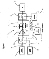
- Figure 1 illustrates a schematic representation of an optical link with a test system in accordance with the present invention
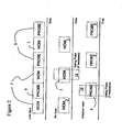
- Figure 2 illustrates a schematic representation of an optical link with an alternative embodiment of the test system in accordance with the present invention
- Figure 3 illustrates a time diagram of the WDM and probe signals
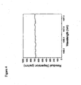
- Figure 4 is a plot of residual dispersion vs wavelength for a WDM populated and amplified link using the test system of Fig. 1 with a standard ODA based on a DPS method;
- Figure 5 is a plot of optical power vs wavelength of a probe signal from the test system of Fig. 1 ;
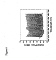
- Figure 6 is a plot of optical power vs wavelength of a WDM signal transmitted through the optical link under test.
- a typical optical network includes a front end 2 with one or a plurality of transmitters for generating one or more optical signals on WDM wavelength channels, each defined by a unique center wavelength, e.g. in the C band between 1520 nm and 1550 nm, and a wavelength division multiplexer for multiplexing the WDM wavelength channels together into a multiplexed wavelength signal 3.
- the multiplexed wavelength signal 3 is transmitted over a typical amplified optical link 4, which includes a length of optical fiber 6 and one or more amplifiers 7, e.g. erbium doped fiber amplifiers (EDFA), for each predetermined length of the optical fiber 6.
- EDFA erbium doped fiber amplifiers
- Switches, add/drop multiplexers and other optical components can also be provided in the amplified optical link 4.
- optical photo-detectors are provided for converting the optical signals back into electrical signals.
- a probe signal 9 is generated by probe signal generator 10, and time division multiplexed (TDM) with the WDM wavelength channel signal 3 prior to being transmitted over the amplified optical link 4, i.e. the link under test.
- TDM time division multiplexed
- a variety of test signals can be used for the probe signal, e.g. the probe signal generator 10 can be a tunable modulated laser for differential phase shift type measurements or a broad band source for fixed analyzer PMD measurements.
- the probe signal 9 must not exceed the maximum optical power threshold for the fiber link 6, and must be spectrally positioned within the operating frequency range of the fiber link, e.g. the C-band between 1520 and 1560 nm and or the L-band between 1560 nm and 1610 nm.
- a first high frequency 2 x 1 TDM optical switch 11 e.g. an acousto-optical (AOM) switch
- a second high frequency 2 x 1 TDM optical switch 12 e.g. an acousto-optical (AOM) switch
- the first switch 11 forms a TDM signal 13 by multiplexing the WDM signal 3 and the probe signal 9 with a modulation frequency of about 1 MHz, which is high enough to be unnoticeable by the EDFA amplifiers 6, and low enough to avoid expensive high-speed switches that implement mux/demux operations along the optical link 4.
- the reaction time of an EDFA is defined by the relaxation time of the erbium ions and the speed of the gain control system, e.g. 10 to 100 ⁇ s, which is too slow to react to fast events, such as input signal modulation over 0.5 MHz, whereby operation of the EDFA amplifiers 7 will be determined by total average input power, assuring that the EDFA behaviour is not affected by the modulation, and enabling measurements to be conducted under the fiber link's operating conditions.
- the modulation frequency can be selected between 0.5 MHz and 100 MHz depending on the type and mode of operation of the amplifiers 7, and the test and measurement (T&M) equipment selected for spectral measurements in probe signal analyzer 14.
- the second switch 12 demultiplexes the TDM signal 13 back into the separate WDM signal 3 and the probe signal 9 for transmission to the receiver end 8 and the analyzer 14, respectively.
- the 1 MHz frequency can be easily achieved by optical gating provided by the AOM switches 11 and 12, thereby enabling a reduction of the gating problem to the selection of appropriate time averaging constants in the probe signal analyzer 14.
- a pulsed optical probe signal 9 is sent to the signal analyzer 14.
- the typical range for time averaging constants for most T&M equipment is longer than milliseconds, so that the pulsed optical probe signal 9 will be averaged by the signal analyzer 14, whereby most T&M equipment can be used with TDM measurements technique in the analyzer 14 without any modification.
- gated detection of the WDM signals is provided to facilitate real time troubleshooting of transmission links, e.g. during PMD-induced outages.
- a 1 MHz electrical pulse 16 is generated by a pulse generator 17 to drive, i.e. set the modulation or clock frequency, the first acousto-optic modulator switch 11.
- the electrical pulse 16 from the pulse generator 17 is also used as a gating pulse, for driving the second acousto-optic modulator switch 12 at the receiver end, whereby the first and second switches 11 and 12 at the ends of optical link 4 are operated in synchronism.
- the gating pulse 16 can be used for gated detection, i.e.
- the second AOM switch 12 is also acting like a time division demultiplexer, see Figure 2 .
- both the first and second AOM switches 11 and 12 are synchronized by a gating pulse generated by the same pulse generator 17, as shown in Figure 1 .
- an electrical gating pulse 16 is not absolutely necessary for the present invention to work.
- an alternative embodiment, illustrated in Figure 3 includes a photo-detector 21 positioned before the second AOM switch 12 to recover the clock frequency of the 1 MHz pulse modulation on the TDM signal 13, which is transmitted to a second pulse generator 22, independent of pulse generator 17.
- the second pulse generator 22 includes electronic circuitry for detecting edges of the pulses in the TDM signal 13 for generating a second electrical pulse 23, which is used to trigger the operation of the second AOM switch 12. Accordingly, it is not necessary to supply the electrical gating pulse 16 from the transmitter end 2 to the receiver end 8, which is difficult when the transmitter end 2 and the receiver end 8 are widely separated. Unfortunately, synchronization of the first and second AOM switches 11 and 12 is not possible if no light reaches the receiver end 8. However, if an electrical gating pulse 16 is supplied to the receiver end 8 from the transmitter end 2, the first and second AOM switches 1 and 12 will operate in synchronism even when no light reaches the receiver, which facilitates trouble shooting the optical link 4.
- the optical link under test 4 contained nine optical amplifiers 7 and about 560-km of single mode fiber (SMF) 8 with a dispersion compensation map (DCM).
- the DCM has been optimized for 10 Gb/s NRZ zero-chirp transmission that resulted in about 7% of undocompensation.
- the optical link 4 was populated with the WDM signal 3 including forty wavelength channels with 100 GHz spacing across the C-band. Timing for the TDM measurements was established according to the diagram shown in Figure 3 .
- the modulation frequency of the first and second AOM switches 11 and 12 was set to 0.7 MHz (limited by available pulse generators) which is slightly lower than desirable switching frequency, so that insignificant reaction from the EDFA amplifiers 7 was expected.
- the probe signal channel 9 from the probe signal generator 10 had about 7 dB higher peak power than average WDM channel in WDM signal 3.
- ODA optical dispersion analyzer
- an optical spectrum taken by the ODA device in the analyzer 14 and illustrating the probe signal 9 at approximately 1545 nm, is presented in Figure 5 .
- the optical spectrum was taken with optical gating with a gate pulse set 16 for the probe signal 9, see Figure 2 , the lower diagram.
- the WDM channels in the WDM signal 3 are successfully suppressed by optical gating by the second AOM switch 12 in front of the analyzer 14.
- Figure 6 illustrates a spectrum received with gating pulse "flipped" to the WDM signal 3, i.e. timing is similar to middle diagram of Figure 2 , showing the wavelength optical channels taken from a monitor output (-20 dB) of the last amplifier 7 in the optical link 4.
- a comparison of the spectra in Figures 5 and 6 shows that the original power difference of 7 dB between the probe and the WDM channels 9 and 3, respectively, has been preserved during propagation through the link 4.
- a single probe channel 9 is able to propagate in a link 4 without draining all the power from the WDM amplifiers 7 and to maintain its peak power well under the nonlinearity threshold.
- a tilt of the ASE baseline in the first spectrum, Figure 5 can be explained by the low modulation frequency used for the first and second AOM switches 11 and 12, so that the optical amplifiers 7 have been slightly reacting to the modulation of the total input optical power from 0 dBm (WDM channels 3) to -10 dBm (ODA probe channel 9). With higher modulation frequency, it is possible to maintain the ASE at the same level that can be successfully used for OSNR measurements in amplified links.
Landscapes
- Engineering & Computer Science (AREA)
- Computer Networks & Wireless Communication (AREA)
- Signal Processing (AREA)
- Physics & Mathematics (AREA)
- Electromagnetism (AREA)
- Optical Communication System (AREA)
Description
- The present invention claims priority from United States Patent Application No.
60/828,484 filed October 6, 2006 - The present invention relates to the testing of optically amplified links, and in particular to the testing of loaded wavelength division multiplexed links with time division multiplexed test signals.
- The performance of optical transmission links is largely determined by the spectral properties of the transmission fiber, the optical amplifiers, the reconfigurable optical add/drop multiplexers (ROADMs), and various other components included in the links. Spectral characterization of assembled and installed transmission links are extremely important for link performance optimization, troubleshooting, and maintenance. Modem wavelength division multiplexed (WDM) networks offer many challenges for test and measurement equipment, in particular to conducting spectral measurements in active WDM links in which optical amplifiers are designed to carry many WDM channels. Currently, spectral measurements in active WDM links are either measured unloaded, i.e. without WDM channels, or loaded, i.e. with WDM channels.
- The unloaded approach, disclosed in
US Patent Publication No. 2004/0165888 in the name Gerstel et al , is not suitable for measurement techniques, such as a differential phase shift (DPS) method, based on a single scanning channel, i.e. a probe channel. To avoid nonlinear impairments in transmitted signals, the total output power of a typical optical amplifier, which is normally shared among 40 or 80 WDM channels, is constant and usually is limited to about +20 dBm, i.e. about +4 dBm per channel for 40 channel system. Accordingly, attempts to measure spectral properties with a single channel will lead to heavy nonlinear impairments, e.g. stimulated Brillouin scattering (SBS) and self phase modulation (SPM), in the probe channel, which make the probe channel virtually undetectable. Measurement techniques based on broad band sources (BBS), similar to the fixed analyzer method for PMD measurements, have worked well with WDM amplifiers; however, in the absence of WDM channels, amplifier noise might significantly reduce the degree of polarization of the original BBS and jeopardize the accuracy of such measurements. Also, BBS methods are applicable only to spectrally averaged types of measurements. - The loaded approach requires frequency demultiplexing of a probe signal with the WDM channels, which is commonly done with an interleaver at the output of the link. The interleaver is used to block the WDM channels from entering an analyzer and disturbing the test measurements. Unfortunately, spectral intervals, adjacent to the WDM channels on the ITU grid, are simply eliminated from the measurements by the interleaver, whereby important spectral information is lost.
- Moreover, both traditional approaches are disruptive for data traffic in the transmission link under test; therefore, they cannot be used for real time correlation between performance and spectral parameters of the link channels, which is important when link parameters are changing, e.g. PMD fluctuations.
- An object of the present invention is to overcome the shortcomings of the prior art by providing a testing system for use in an active WDM optical link providing a variety of spectral measurements under normal operating conditions of the fiber link.
- Accordingly, the present invention relates to a system for testing an optical link, while a wavelength division multiplexed (WDM) signal with a plurality of wavelength channels is being transmitted, comprising:
- a probe signal generator for generating a probe signal which does not exceed the maximum optical power threshold for the fiber link and is spectrally positioned within the operating frequency of the fiber link;
- a first time division multiplexing (TDM) optical switch for time division multiplexing the probe signal with the WDM signal forming a TDM signal;
- a second TDM optical switch for separating the probe signal from the WDM signal after the TDM signal has traversed the optical link; and
- an analyzer for receiving the probe signal from the second TDM switch, and for conducting tests on the probe signal.
- The invention will be described in greater detail with reference to the accompanying drawings which represent preferred embodiments thereof, wherein:
-
Figure 1 illustrates a schematic representation of an optical link with a test system in accordance with the present invention; -
Figure 2 illustrates a schematic representation of an optical link with an alternative embodiment of the test system in accordance with the present invention; -
Figure 3 illustrates a time diagram of the WDM and probe signals; -
Figure 4 is a plot of residual dispersion vs wavelength for a WDM populated and amplified link using the test system ofFig. 1 with a standard ODA based on a DPS method; -
Figure 5 is a plot of optical power vs wavelength of a probe signal from the test system ofFig. 1 ; and -
Figure 6 is a plot of optical power vs wavelength of a WDM signal transmitted through the optical link under test. - With reference to
Figure 1 , a typical optical network, generally indicated at 1, includes afront end 2 with one or a plurality of transmitters for generating one or more optical signals on WDM wavelength channels, each defined by a unique center wavelength, e.g. in the C band between 1520 nm and 1550 nm, and a wavelength division multiplexer for multiplexing the WDM wavelength channels together into a multiplexedwavelength signal 3. Themultiplexed wavelength signal 3 is transmitted over a typical amplifiedoptical link 4, which includes a length ofoptical fiber 6 and one ormore amplifiers 7, e.g. erbium doped fiber amplifiers (EDFA), for each predetermined length of theoptical fiber 6. Switches, add/drop multiplexers and other optical components can also be provided in the amplifiedoptical link 4. At thereceiver end 8, optical photo-detectors are provided for converting the optical signals back into electrical signals. - In accordance with the present invention, a
probe signal 9 is generated byprobe signal generator 10, and time division multiplexed (TDM) with the WDMwavelength channel signal 3 prior to being transmitted over the amplifiedoptical link 4, i.e. the link under test. A variety of test signals can be used for the probe signal, e.g. theprobe signal generator 10 can be a tunable modulated laser for differential phase shift type measurements or a broad band source for fixed analyzer PMD measurements. Theprobe signal 9 must not exceed the maximum optical power threshold for thefiber link 6, and must be spectrally positioned within the operating frequency range of the fiber link, e.g. the C-band between 1520 and 1560 nm and or the L-band between 1560 nm and 1610 nm. To perform TDM, a first high frequency 2 x 1 TDMoptical switch 11, e.g. an acousto-optical (AOM) switch, is positioned at the input of the link undertest 4, and a second high frequency 2 x 1 TDMoptical switch 12, e.g. an acousto-optical (AOM) switch, is positioned at the output of the link undertest 4. Thefirst switch 11 forms aTDM signal 13 by multiplexing theWDM signal 3 and theprobe signal 9 with a modulation frequency of about 1 MHz, which is high enough to be unnoticeable by the EDFAamplifiers 6, and low enough to avoid expensive high-speed switches that implement mux/demux operations along theoptical link 4. The reaction time of an EDFA is defined by the relaxation time of the erbium ions and the speed of the gain control system, e.g. 10 to 100 µs, which is too slow to react to fast events, such as input signal modulation over 0.5 MHz, whereby operation of theEDFA amplifiers 7 will be determined by total average input power, assuring that the EDFA behaviour is not affected by the modulation, and enabling measurements to be conducted under the fiber link's operating conditions. In practice the modulation frequency can be selected between 0.5 MHz and 100 MHz depending on the type and mode of operation of theamplifiers 7, and the test and measurement (T&M) equipment selected for spectral measurements inprobe signal analyzer 14. Practical ranges are 0.5 MHz to 10 MHz, 1.0 MHz to 10 MHz, 0.5 MHz to 5 MHz, and 1.0 MHz to 5 MHz; however, faster ranges, e.g. 2 to 100 MHz, 10 MHz and above, and 10 MHz to 100MHz, are also advantageous. Thesecond switch 12 demultiplexes theTDM signal 13 back into theseparate WDM signal 3 and theprobe signal 9 for transmission to thereceiver end 8 and theanalyzer 14, respectively. - While electronic gating at 1 MHz time scale would have been a problem for most T&M equipment, the 1 MHz frequency can be easily achieved by optical gating provided by the
AOM switches probe signal analyzer 14. As a result of optical demultiplexing by thesecond switch 12, a pulsedoptical probe signal 9 is sent to thesignal analyzer 14. In fact, the typical range for time averaging constants for most T&M equipment is longer than milliseconds, so that the pulsedoptical probe signal 9 will be averaged by thesignal analyzer 14, whereby most T&M equipment can be used with TDM measurements technique in theanalyzer 14 without any modification. - Preferably, gated detection of the WDM signals is provided to facilitate real time troubleshooting of transmission links, e.g. during PMD-induced outages. When gated detection is used, a 1 MHz
electrical pulse 16 is generated by apulse generator 17 to drive, i.e. set the modulation or clock frequency, the first acousto-optic modulator switch 11. Theelectrical pulse 16 from thepulse generator 17 is also used as a gating pulse, for driving the second acousto-optic modulator switch 12 at the receiver end, whereby the first andsecond switches optical link 4 are operated in synchronism. Accordingly, thegating pulse 16 can be used for gated detection, i.e. to switch thesecond switch 12, so that theprobe signal 9 is directed to theanalyzer 14 only when theprobe signal 9 is present in theTDM signal 13, and so that theWDM signal 3 is directed to thereceiver end 8 only when theWDM signal 3 is present in theTDM signal 13. Accordingly, thesecond AOM switch 12 is also acting like a time division demultiplexer, seeFigure 2 . - If practical, both the first and
second AOM switches same pulse generator 17, as shown inFigure 1 . However, anelectrical gating pulse 16 is not absolutely necessary for the present invention to work. For measurements in long-haul links, when the input and the output of theoptical link 4 physically cannot be connected to thesame generator 17, an alternative embodiment, illustrated inFigure 3 , includes a photo-detector 21 positioned before thesecond AOM switch 12 to recover the clock frequency of the 1 MHz pulse modulation on theTDM signal 13, which is transmitted to asecond pulse generator 22, independent ofpulse generator 17. Thesecond pulse generator 22 includes electronic circuitry for detecting edges of the pulses in theTDM signal 13 for generating a secondelectrical pulse 23, which is used to trigger the operation of thesecond AOM switch 12. Accordingly, it is not necessary to supply theelectrical gating pulse 16 from thetransmitter end 2 to thereceiver end 8, which is difficult when thetransmitter end 2 and thereceiver end 8 are widely separated. Unfortunately, synchronization of the first and second AOM switches 11 and 12 is not possible if no light reaches thereceiver end 8. However, if anelectrical gating pulse 16 is supplied to thereceiver end 8 from thetransmitter end 2, the first andsecond AOM switches optical link 4. - Electrical gating can be applied to a bit error rate test (BERT) to provide real time BER measurements, which then can be correlated with real time spectral measurements obtained by the
spectral analyzer 14. Fundamentally, time resolution of correlation measurements is limited by the time constant in thespectral analyzer 14 and the error accumulation time required for statistically stable BER measurements, i.e. for a given time constant (averaging time), thespectral analyzer 14 cannot detect and correlate events that are faster (shorter) then this time constant. Therefore, time resolution down to a few dozens of seconds seems to be feasible. None of the currently available traditional measurement techniques can offer similar correlation measurements due to inherently sequential approach: performance measurements have to be done before or after spectral ones. - To verify the operational principle of the TDM technique according to the present invention, two experiments were conducted with a fully functional WDM amplified link. In both experiments, the optical link under
test 4 contained nineoptical amplifiers 7 and about 560-km of single mode fiber (SMF) 8 with a dispersion compensation map (DCM). The DCM has been optimized for 10 Gb/s NRZ zero-chirp transmission that resulted in about 7% of undocompensation. Theoptical link 4 was populated with theWDM signal 3 including forty wavelength channels with 100 GHz spacing across the C-band. Timing for the TDM measurements was established according to the diagram shown inFigure 3 . The modulation frequency of the first and second AOM switches 11 and 12 was set to 0.7 MHz (limited by available pulse generators) which is slightly lower than desirable switching frequency, so that insignificant reaction from theEDFA amplifiers 7 was expected. At thefirst AOM switch 11, theprobe signal channel 9 from theprobe signal generator 10 had about 7 dB higher peak power than average WDM channel inWDM signal 3. - During the first experiment, a commercial optical dispersion analyzer (ODA) based on differential-phase shift method was used in the
analyzer 14. Operation parameters or design of the ODA device were not adjusted or modified in any way. With TDM techniques in operation, the ODA was able to collect all required data, i.e. cumulative gain/insertion loss, group delay, PDL, DGD, etc., for the fully populated amplifiedlink 4.Figure 4 graphically illustrates a fragment of measured CD dependence, in which a measured average CD value of 700 ps/nm is in agreement with expected residual dispersion of the link calculated based on SMF and DCF specifications, and the used dispersion compensation map. - In accordance with the present invention, an optical spectrum, taken by the ODA device in the
analyzer 14 and illustrating theprobe signal 9 at approximately 1545 nm, is presented inFigure 5 . The optical spectrum was taken with optical gating with a gate pulse set 16 for theprobe signal 9, seeFigure 2 , the lower diagram. The WDM channels in theWDM signal 3 are successfully suppressed by optical gating by thesecond AOM switch 12 in front of theanalyzer 14.Figure 6 illustrates a spectrum received with gating pulse "flipped" to theWDM signal 3, i.e. timing is similar to middle diagram ofFigure 2 , showing the wavelength optical channels taken from a monitor output (-20 dB) of thelast amplifier 7 in theoptical link 4. - A comparison of the spectra in
Figures 5 and6 shows that the original power difference of 7 dB between the probe and theWDM channels link 4. Hence, due to time multiplexing, asingle probe channel 9 is able to propagate in alink 4 without draining all the power from theWDM amplifiers 7 and to maintain its peak power well under the nonlinearity threshold. A tilt of the ASE baseline in the first spectrum,Figure 5 , can be explained by the low modulation frequency used for the first and second AOM switches 11 and 12, so that theoptical amplifiers 7 have been slightly reacting to the modulation of the total input optical power from 0 dBm (WDM channels 3) to -10 dBm (ODA probe channel 9). With higher modulation frequency, it is possible to maintain the ASE at the same level that can be successfully used for OSNR measurements in amplified links. - For the second experiment, a JDSU T-BERD 8000® with a PMD module and a complimentary broad band source OBS-15a® and variable polarizer OVP-15® is used to measure average PMD in the amplified
link 4. The average PMD value was found to be 1.45 ps, which is in reasonable agreement with the previous results. Again, the TDM measurement technique worked well without any modification or adjustment of standard T&M equipment inanalyzer 14.
Claims (11)
- A system for testing an optical link (4), while a wavelength division multiplexed (WDM) signal (3) with a plurality of wavelength channels is being transmitted, comprising:a probe signal generator (10) for generating a probe signal (9) which is spectrally positioned within the operating frequency range of the fiber link (4);characterized in that the probe signal (9) does not exceed the maximum optical power threshold for the fiber link (4) and in that the system further comprises:a first time division multiplexing (TDM) optical switch (11) for time division multiplexing the probe signal (9) with the WDM signal (3) forming a TDM signal (13);a second TDM optical switch (12) for separating the probe signal (9) from the WDM signal (3) after the TDM signal (13) has traversed the optical link (4); andan analyzer (14) for receiving the probe signal (9) from the second TDM switch (12), and for conducting tests on the probe signal (9).
- The system according to claim 1, wherein the first TDM switch (11) has a modulation frequency of between 0.5 MHz and 100 MHz.
- The system according to claim 1, wherein the first TDM switch (11) has a modulation frequency of about 1 MHz to 10 MHz.
- The system according to any of claims 1, 2 or 3, further comprising a gating signal generator (17) connected to the second TDM switch (12) for generating a gating signal (16) indicative of the modulation frequency of the TDM signal (13) for use in separating the probe signal (9) from the WDM signal (3).
- The system according to claim 4, wherein the gating signal generator (17) is also connected to the first TDM switch (11) for setting the modulation frequency thereof.
- The system according to claim 4, further comprising a photo-detector (21) connected to the gating signal generator (17) for detecting the modulation frequency of the TDM signal (13); and
a clock signal generator (22), independent of the gating signal generator (17), connected to the first TDM switch (11) for generating a clock signal (23) to set the modulation frequency of the TDM signal (13). - The system according to any one of claims 1 to 6, wherein the probe signal generator (10) comprises a tunable modulated laser for generating probe signals defined by different center wavelengths.
- The system according to claim 7, wherein the probe signal (9) is tuneable to a wavelength between 1520 nm and 1610 nm.
- The system according to any one of claims 1 to 8, wherein each of the first and second TDM switches (11,12) comprises an acousto-optic modulator switch.
- The system according to any one of claims 1 to 6, wherein the probe signal generator (10) comprises a broad band source.
- The system according to claim 10, wherein the probe signal (9) covers a wavelength range from 1520 nm to 1560 nm and/or 1560 nm to 1610 nm.
Applications Claiming Priority (1)
| Application Number | Priority Date | Filing Date | Title |
|---|---|---|---|
| US82848406P | 2006-10-06 | 2006-10-06 |
Publications (2)
| Publication Number | Publication Date |
|---|---|
| EP1909412A1 EP1909412A1 (en) | 2008-04-09 |
| EP1909412B1 true EP1909412B1 (en) | 2009-12-23 |
Family
ID=38846921
Family Applications (1)
| Application Number | Title | Priority Date | Filing Date |
|---|---|---|---|
| EP07253901A Active EP1909412B1 (en) | 2006-10-06 | 2007-10-02 | Testing optically amplified links with time-division multiplexed test signals |
Country Status (5)
| Country | Link |
|---|---|
| US (1) | US7925158B2 (en) |
| EP (1) | EP1909412B1 (en) |
| CN (1) | CN101159493B (en) |
| DE (1) | DE602007003926D1 (en) |
| ES (1) | ES2338715T3 (en) |
Families Citing this family (13)
| Publication number | Priority date | Publication date | Assignee | Title |
|---|---|---|---|---|
| US8190024B2 (en) * | 2008-05-12 | 2012-05-29 | Verizon Patent And Licensing Inc. | Systems and methods for wavelength scanning of in-service wavelength division multiplexing systems |
| US8811815B2 (en) * | 2009-04-20 | 2014-08-19 | Verizon Patent And Licensing Inc. | Optical network testing |
| US9106051B1 (en) * | 2014-07-02 | 2015-08-11 | Northrop Grumman Systems Corporation | Multi-wavelength seed source for coherent fiber amplifiers |
| WO2016061183A1 (en) | 2014-10-14 | 2016-04-21 | The Arizona Board Of Regents On Behalf Of The University Of Arizona | Multi-wavelength balanced optical transmission networks |
| CN105790830B (en) * | 2014-12-26 | 2018-11-20 | 华为技术有限公司 | Optical module is in position detecting method and device |
| JP2019503120A (en) * | 2015-12-03 | 2019-01-31 | ザ アリゾナ ボード オブ リージェンツ オン ビハーフ オブ ザ ユニバーシティー オブ アリゾナThe Arizona Board of Regents on behalf of The University of Arizona | Fast exploration of signal quality in WDM networks |
| WO2018156752A1 (en) * | 2017-02-22 | 2018-08-30 | Arizona Board Of Regents On Behalf Of The University Of Arizona | Fast edfa gain spectrum characterization using weak probe and fourier sampling |
| CN112054841A (en) * | 2019-06-06 | 2020-12-08 | 中国移动通信有限公司研究院 | Active module, mobile communication forwarding system and mobile communication forwarding control method |
| CN110429991A (en) * | 2019-07-16 | 2019-11-08 | 国网江苏省电力有限公司电力科学研究院 | A simulation test system for electric energy data acquisition |
| US11791925B2 (en) * | 2021-11-08 | 2023-10-17 | Huawei Technologies Co., Ltd. | Method, apparatus and system for determining multipath interference (MPI) on an optical link |
| WO2023119673A1 (en) * | 2021-12-24 | 2023-06-29 | 学校法人明治大学 | Evaluation device, light receiver, optical communication system, program, and evaluation method |
| US20240283532A1 (en) * | 2023-02-20 | 2024-08-22 | Exfo Inc. | All-optical open cable osnr measurement |
| CN119522545B (en) | 2023-06-22 | 2026-01-13 | 学校法人明治大学 | Control device, compensation device, program, and control method |
Family Cites Families (15)
| Publication number | Priority date | Publication date | Assignee | Title |
|---|---|---|---|---|
| JPS61166235A (en) * | 1985-01-18 | 1986-07-26 | Matsushita Electric Ind Co Ltd | Pcm optical transmitter |
| JPS63171051A (en) * | 1987-01-09 | 1988-07-14 | Hitachi Ltd | Equipment diagnosis method |
| US6175416B1 (en) * | 1996-08-06 | 2001-01-16 | Brown University Research Foundation | Optical stress generator and detector |
| US7181138B1 (en) | 1998-12-14 | 2007-02-20 | Tellabs Operations, Inc. | Optical network connection test apparatus and methods |
| JP2001274772A (en) * | 2000-03-24 | 2001-10-05 | Kddi Corp | TDM optical multiplexer, TDM optical separator, WDM / TDM converter, and TDM / WDM converter |
| JP2001308417A (en) * | 2000-04-18 | 2001-11-02 | Ando Electric Co Ltd | Optical amplifier evaluation method and optical amplifier evaluation apparatus |
| US6542233B1 (en) * | 2000-10-04 | 2003-04-01 | Nortel Networks Limited | Method and apparatus for the measurement of erbium optical amplifiers |
| JP3880873B2 (en) * | 2002-03-06 | 2007-02-14 | 富士通株式会社 | Multiple optical path interference light measuring method and measuring apparatus |
| JP2004064148A (en) * | 2002-07-24 | 2004-02-26 | Nippon Telegr & Teleph Corp <Ntt> | Optical time division multiplexed signal channel identification method and apparatus |
| US7386231B2 (en) * | 2003-02-04 | 2008-06-10 | Sunrise Telecom Incorporated | Method and apparatus for testing network data signals in a wavelength division multiplexed optical network |
| CN100388651C (en) * | 2004-06-24 | 2008-05-14 | 烽火通信科技股份有限公司 | A 40G optical transmission system bit error rate detection method and apparatus |
| US7711266B1 (en) * | 2004-12-07 | 2010-05-04 | Sprint Communications Company L.P. | PMD measurements for an in-service fiber span |
| US7403712B2 (en) * | 2005-02-22 | 2008-07-22 | Northrop Grumman Corporation | Matrix time division multiplex (MTDM) interrogation |
| US7826745B2 (en) * | 2005-12-21 | 2010-11-02 | International Business Machines Corporation | Open fiber control and loss of light propagation in time division multiplexed inter-system channel link |
| US7787765B2 (en) * | 2005-12-21 | 2010-08-31 | International Business Machines Corporation | Method and apparatus device for initializing an end-to-end link in a fiber optic communications system |
-
2007
- 2007-10-02 DE DE602007003926T patent/DE602007003926D1/en active Active
- 2007-10-02 EP EP07253901A patent/EP1909412B1/en active Active
- 2007-10-02 ES ES07253901T patent/ES2338715T3/en active Active
- 2007-10-03 US US11/866,575 patent/US7925158B2/en active Active
- 2007-10-08 CN CN2007101641614A patent/CN101159493B/en active Active
Also Published As
| Publication number | Publication date |
|---|---|
| CN101159493A (en) | 2008-04-09 |
| US20080085115A1 (en) | 2008-04-10 |
| CN101159493B (en) | 2012-03-28 |
| EP1909412A1 (en) | 2008-04-09 |
| DE602007003926D1 (en) | 2010-02-04 |
| US7925158B2 (en) | 2011-04-12 |
| ES2338715T3 (en) | 2010-05-11 |
Similar Documents
| Publication | Publication Date | Title |
|---|---|---|
| US7925158B2 (en) | Testing optically amplified links with time-division multiplexed test signals | |
| Lee et al. | OSNR monitoring technique using polarization-nulling method | |
| EP2569879B1 (en) | Method and apparatus for determining an optical signal-to-noise ratio (osnr) penalty | |
| EP0667688B1 (en) | A noise measurement for optical amplifier and a system therefor | |
| US20120219285A1 (en) | In-band optical signal to noise ratio monitoring technique | |
| EP2264916A1 (en) | OSNR monitor device and OSNR measurement device | |
| JPH118590A (en) | Optical transmission system and supervisory and control method therefor | |
| US7912370B2 (en) | Optical power measurement apparatus and optical power measurement method | |
| US6607311B1 (en) | Method and system transmitting optical signals generated by multi-line sources via WDM optical network | |
| JP2004289707A (en) | Method and apparatus for monitoring quality of wavelength multiplexed optical signal and optical transmission system using the same | |
| US20050047791A1 (en) | Dispersion compensation control method and apparatus thereof and optical transmission method and system thereof | |
| US6814376B2 (en) | Method and system for generating short pulse signals | |
| US8190024B2 (en) | Systems and methods for wavelength scanning of in-service wavelength division multiplexing systems | |
| US8498536B2 (en) | Dispersion measurement of optical fibres during operation | |
| Sinkin et al. | Impact of broadband four-wave mixing on system characterization | |
| JP4786383B2 (en) | Optical transmitter | |
| Daikoku et al. | 160 Gbit/s-based field transmission experiments with single-polarization RZ-DPSK signals and simple PMD compensator | |
| Buchali et al. | Eye monitoring in a 160 Gbit/s RZ field transmission system | |
| Pei et al. | Characterizing Fiber Nonlinearity with Deployed Equipment in Optical Line Systems | |
| Marcenac et al. | 80 Gbit/s OTDM using electroabsorption modulators | |
| Anderson et al. | Experimental Demonstration of Multi-Impairment Monitoring on a commercial 10 Gbit/s NRZ WDM channel | |
| Calvani et al. | Ultra-stable polarization independent all-optical demultiplexer using four wave mixing in a dispersion shifted fiber | |
| Su et al. | WDM Optical Steganography Based on Super-Continuum Light Source | |
| Clausen et al. | Pilot tone modulation used for channel identification in OTDM networks | |
| JP2000357992A (en) | Optical transmission line and optical transmission system |
Legal Events
| Date | Code | Title | Description |
|---|---|---|---|
| PUAI | Public reference made under article 153(3) epc to a published international application that has entered the european phase |
Free format text: ORIGINAL CODE: 0009012 |
|
| AK | Designated contracting states |
Kind code of ref document: A1 Designated state(s): AT BE BG CH CY CZ DE DK EE ES FI FR GB GR HU IE IS IT LI LT LU LV MC MT NL PL PT RO SE SI SK TR |
|
| AX | Request for extension of the european patent |
Extension state: AL BA HR MK RS |
|
| 17P | Request for examination filed |
Effective date: 20081001 |
|
| 17Q | First examination report despatched |
Effective date: 20081106 |
|
| AKX | Designation fees paid |
Designated state(s): DE ES FR GB |
|
| GRAP | Despatch of communication of intention to grant a patent |
Free format text: ORIGINAL CODE: EPIDOSNIGR1 |
|
| GRAS | Grant fee paid |
Free format text: ORIGINAL CODE: EPIDOSNIGR3 |
|
| GRAA | (expected) grant |
Free format text: ORIGINAL CODE: 0009210 |
|
| AK | Designated contracting states |
Kind code of ref document: B1 Designated state(s): DE ES FR GB |
|
| REG | Reference to a national code |
Ref country code: GB Ref legal event code: FG4D |
|
| REF | Corresponds to: |
Ref document number: 602007003926 Country of ref document: DE Date of ref document: 20100204 Kind code of ref document: P |
|
| REG | Reference to a national code |
Ref country code: ES Ref legal event code: FG2A Ref document number: 2338715 Country of ref document: ES Kind code of ref document: T3 |
|
| PLBE | No opposition filed within time limit |
Free format text: ORIGINAL CODE: 0009261 |
|
| STAA | Information on the status of an ep patent application or granted ep patent |
Free format text: STATUS: NO OPPOSITION FILED WITHIN TIME LIMIT |
|
| 26N | No opposition filed |
Effective date: 20100924 |
|
| REG | Reference to a national code |
Ref country code: GB Ref legal event code: 732E Free format text: REGISTERED BETWEEN 20141106 AND 20141112 |
|
| REG | Reference to a national code |
Ref country code: FR Ref legal event code: PLFP Year of fee payment: 9 |
|
| REG | Reference to a national code |
Ref country code: FR Ref legal event code: PLFP Year of fee payment: 10 |
|
| REG | Reference to a national code |
Ref country code: FR Ref legal event code: PLFP Year of fee payment: 11 |
|
| REG | Reference to a national code |
Ref country code: FR Ref legal event code: PLFP Year of fee payment: 11 |
|
| REG | Reference to a national code |
Ref country code: FR Ref legal event code: PLFP Year of fee payment: 12 |
|
| PGFP | Annual fee paid to national office [announced via postgrant information from national office to epo] |
Ref country code: DE Payment date: 20241029 Year of fee payment: 18 |
|
| PGFP | Annual fee paid to national office [announced via postgrant information from national office to epo] |
Ref country code: GB Payment date: 20251031 Year of fee payment: 19 |
|
| PGFP | Annual fee paid to national office [announced via postgrant information from national office to epo] |
Ref country code: FR Payment date: 20251028 Year of fee payment: 19 |
|
| PGFP | Annual fee paid to national office [announced via postgrant information from national office to epo] |
Ref country code: ES Payment date: 20251106 Year of fee payment: 19 |