EP1906173A2 - Method of measuring degree of crystallinity of polycrystalline silicon substrate, method of fabricating organic light emitting display using the same, and organic light emitting display fabricated using the same - Google Patents
Method of measuring degree of crystallinity of polycrystalline silicon substrate, method of fabricating organic light emitting display using the same, and organic light emitting display fabricated using the same Download PDFInfo
- Publication number
- EP1906173A2 EP1906173A2 EP06256561A EP06256561A EP1906173A2 EP 1906173 A2 EP1906173 A2 EP 1906173A2 EP 06256561 A EP06256561 A EP 06256561A EP 06256561 A EP06256561 A EP 06256561A EP 1906173 A2 EP1906173 A2 EP 1906173A2
- Authority
- EP
- European Patent Office
- Prior art keywords
- silicon substrate
- crystallinity
- peak
- degree
- polycrystalline silicon
- Prior art date
- Legal status (The legal status is an assumption and is not a legal conclusion. Google has not performed a legal analysis and makes no representation as to the accuracy of the status listed.)
- Withdrawn
Links
Images




Classifications
-
- G—PHYSICS
- G01—MEASURING; TESTING
- G01N—INVESTIGATING OR ANALYSING MATERIALS BY DETERMINING THEIR CHEMICAL OR PHYSICAL PROPERTIES
- G01N21/00—Investigating or analysing materials by the use of optical means, i.e. using sub-millimetre waves, infrared, visible or ultraviolet light
- G01N21/62—Systems in which the material investigated is excited whereby it emits light or causes a change in wavelength of the incident light
- G01N21/63—Systems in which the material investigated is excited whereby it emits light or causes a change in wavelength of the incident light optically excited
- G01N21/65—Raman scattering
-
- H—ELECTRICITY
- H10—SEMICONDUCTOR DEVICES; ELECTRIC SOLID-STATE DEVICES NOT OTHERWISE PROVIDED FOR
- H10P—GENERIC PROCESSES OR APPARATUS FOR THE MANUFACTURE OR TREATMENT OF DEVICES COVERED BY CLASS H10
- H10P74/00—Testing or measuring during manufacture or treatment of wafers, substrates or devices
Definitions
- the present invention relates to a method of measuring a degree of crystallinity of a polycrystalline silicon substrate, a method of fabricating an organic light emitting display using the same, and an organic light emitting display fabricated using the same, and, more particularly, to a method of measuring a degree of crystallinity of a polycrystalline silicon substrate using a Raman spectrum graph, a method of fabricating an organic light emitting display using the same, and an organic light emitting display fabricated using the same.
- polycrystalline silicon has a high mobility compared to amorphous silicon (a-Si for short), polycrystalline silicon is used in various electronic devices such as solar cells and flat panel displays.
- the mobility of polycrystalline silicon is related to a degree of crystallinity of the polycrystalline silicon.
- Methods of estimating the degree of crystallinity may include a Raman spectroscopic analysis method.
- spectral lines having a longer or shorter wavelength than the wavelength of the incident light are observed in addition to a spectral line having the wavelength of the incident light. This phenomenon is known as the Raman effect.
- a Raman spectroscopic analysis method uses the Raman effect.
- the degree of crystallinity of the polycrystalline silicon is estimated based on a full width at half maximum (FWHM) of a Raman spectrum graph. Specifically, as the FWHM of the Raman spectrum graph decreases, the degree of crystallinity of the polycrystalline silicon increases.
- FWHM full width at half maximum
- the method of measuring the degree of crystallinity based on the FWHM of the Raman spectrum graph has a problem in that the method tends to be unreliable.
- the aforementioned method of measuring the degree of crystallinity has a problem in that the method does not consider the dispersion of a threshold voltage (Vth) that is an important characteristic of a thin film transistor.
- Vth threshold voltage
- the invention sets out to provide a more reliable method of measuring a degree of crystallinity of a polycrystalline silicon substrate.
- the invention seeks to provide an organic light emitting display having excellent electrical characteristics such as mobility and threshold voltage dispersion, and a method of fabricating the same.
- a method of measuring a degree of crystallinity of a polycrystalline silicon comprises the features of claim 1.
- Preferred features of this aspect of the invention are set out in claims 2 to 4.
- a method of fabricating an organic light emitting display is set out in claim 5.
- Preferred features of this aspect of the invention are as set out in claims 6 to 10.
- a third aspect of the invention provides an organic light emitting display as set out in claim 11.
- the amorphous peak has a centre at 480 cm-1, and the polycrystalline peak has a centre at 517 cm-1.
- FIGS. 2 to 4 are Raman spectrum graphs of polycrystalline silicon substrates having different degrees of crystallinity. As can be seen from FIGS. 2 to 4, each of these Raman spectrum graphs has a different FWHM.
- the degree of crystallinity is measured to be 32.8% from the Raman spectrum graph of FIG. 2, the degree of crystallinity is measured to be 49.7% from the Raman spectrum graph of FIG. 3, and the degree of crystallinity is measured to be 75.5% from the Raman spectrum graph of FIG. 4.
- FIG. 5 is a graph of a PMOS threshold voltage and a full width at half maximum (FWHM) of a Raman spectrum graph according to a degree of crystallinity of the polycrystalline substrate.
- FWHM full width at half maximum
- FIG. 6 is a graph of an ID-Vg characteristic of the polycrystalline silicon substrate having a degree of crystallinity of 32.8%
- FIG. 7 is a graph of an ID-Vg characteristic of the polycrystalline silicon substrate having a degree of crystallinity of 49.7%
- FIG. 8 is a graph of an ID-Vg characteristic of the polycrystalline silicon substrate having a degree of crystallinity of 75.5%.
- the method of fabricating the organic light emitting display comprises fabricating a polycrystalline silicon substrate by crystallizing an amorphous silicon substrate at block S100; obtaining a Raman spectrum graph by irradiating the polycrystalline silicon substrate with monochromatic light, such as a laser beam or any other suitable monochromatic light, at block S200; examining a degree of crystallinity of the polycrystalline silicon substrate based on the Raman spectrum graph at block S300; and fabricating a thin film transistor at block S400.
- monochromatic light such as a laser beam or any other suitable monochromatic light
- the fabricating of the polycrystalline silicon substrate (S100) may be performed using a solid phase crystallization (SPC) method, an excimer laser annealing (ELA) method, a metal induced crystallization (MIC) method, a metal induced lateral crystallization (MILC) method, or a sequential lateral solidification (SLS) method.
- SPC solid phase crystallization
- ELA excimer laser annealing
- MIC metal induced crystallization
- MILC metal induced lateral crystallization
- SLS sequential lateral solidification
- the SPC method is a method of crystallizing the amorphous silicon substrate by using a high temperature heat treatment.
- the ELA method is a method in which an upper portion of the amorphous silicon substrate is instantaneously melted and recrystallized by irradiating the amorphous silicon substrate with an excimer laser beam.
- the MIC method is a method in which a metal catalyst is coated on the amorphous silicon substrate using a sputtering method or a spin coating method to induce crystallization at a low temperature.
- the MILC method is a method in which metal seeds are deposited on source and drain regions of the amorphous silicon substrate, and crystallization proceeds laterally in the amorphous silicon substrate away from the metal seeds at a low temperature.
- the SLS method is a method in which the amorphous silicon substrate is irradiated with a laser beam two or more times to laterally grow silicon crystal grains to crystallize the amorphous silicon substrate.
- the polycrystalline silicon substrate that is crystallized using any of the aforementioned methods is examined during the examination of the degree of crystallinity using the method of measuring the degree of crystallinity of the polycrystalline silicon substrate according to an embodiment of the invention.
- a Raman spectrum graph is obtained by irradiating the polycrystalline silicon substrate with monochromatic light, such as a laser beam or any other suitable monochromatic light, at block S200; and the degree of crystallinity of the polycrystalline silicon substrate is examined using the method of measuring the degree of crystallinity according to an embodiment of the invention at block S300, shown in FIG.9.
- the thin film transistor used for the organic light emitting display is fabricated using the polycrystalline silicon substrate having a degree of crystallinity that is 70% or more at block S400.
- the threshold voltage dispersion causing non-homogeneity of luminance is more important than the absolute value of an electrical characteristic such as mobility or threshold voltage.
- the threshold voltage dispersion When the threshold voltage dispersion is 1.0V or more, serious non-homogeneity of the luminance occurs even if a circuit for compensating for the threshold voltage dispersion is used.
- the thin film transistor used for the organic light emitting display is fabricated at block S400 using a polycrystalline silicon substrate that is determined to have a degree of crystallinity of 70% or more in the examining of the degree of crystallinity at block S300, while any polycrystalline silicon substrate determined to have a degree of crystallinity of less than 70% is classified as a defective substrate at block S500.
- the invention is not limited to using a degree of crystallinity of 70% as a threshold value at block S300 to determine whether a polycrystalline silicon substrate will be used to fabricate a thin film transistor at block S400, or will be classified as a defective substrate at block 500, and other degrees of crystallinity may be used as a threshold value at block 300 depending on the desired characteristics of the thin film transistor to be fabricated.
- an organic light emitting display having excellent mobility and threshold voltage dispersion characteristics can be provided by using a reliable method of measuring the degree of crystallinity of the polycrystalline silicon substrate.
Landscapes
- Health & Medical Sciences (AREA)
- Nuclear Medicine, Radiotherapy & Molecular Imaging (AREA)
- Physics & Mathematics (AREA)
- Life Sciences & Earth Sciences (AREA)
- Chemical & Material Sciences (AREA)
- Analytical Chemistry (AREA)
- Biochemistry (AREA)
- General Health & Medical Sciences (AREA)
- General Physics & Mathematics (AREA)
- Immunology (AREA)
- Pathology (AREA)
- Thin Film Transistor (AREA)
- Electroluminescent Light Sources (AREA)
- Recrystallisation Techniques (AREA)
- Investigating, Analyzing Materials By Fluorescence Or Luminescence (AREA)
- Crystals, And After-Treatments Of Crystals (AREA)
Abstract
Description
- The present invention relates to a method of measuring a degree of crystallinity of a polycrystalline silicon substrate, a method of fabricating an organic light emitting display using the same, and an organic light emitting display fabricated using the same, and, more particularly, to a method of measuring a degree of crystallinity of a polycrystalline silicon substrate using a Raman spectrum graph, a method of fabricating an organic light emitting display using the same, and an organic light emitting display fabricated using the same.
- Since polycrystalline silicon has a high mobility compared to amorphous silicon (a-Si for short), polycrystalline silicon is used in various electronic devices such as solar cells and flat panel displays.
- The mobility of polycrystalline silicon is related to a degree of crystallinity of the polycrystalline silicon. Methods of estimating the degree of crystallinity may include a Raman spectroscopic analysis method.
- When a transparent material is irradiated with an intense monochromatic light and the spectrum of light scattered from the transparent material is analyzed, spectral lines having a longer or shorter wavelength than the wavelength of the incident light are observed in addition to a spectral line having the wavelength of the incident light. This phenomenon is known as the Raman effect. A Raman spectroscopic analysis method uses the Raman effect.
- In general, the degree of crystallinity of the polycrystalline silicon is estimated based on a full width at half maximum (FWHM) of a Raman spectrum graph. Specifically, as the FWHM of the Raman spectrum graph decreases, the degree of crystallinity of the polycrystalline silicon increases.
- However, the method of measuring the degree of crystallinity based on the FWHM of the Raman spectrum graph has a problem in that the method tends to be unreliable.
- In addition, the aforementioned method of measuring the degree of crystallinity has a problem in that the method does not consider the dispersion of a threshold voltage (Vth) that is an important characteristic of a thin film transistor.
- The invention sets out to provide a more reliable method of measuring a degree of crystallinity of a polycrystalline silicon substrate.
- In addition, the invention seeks to provide an organic light emitting display having excellent electrical characteristics such as mobility and threshold voltage dispersion, and a method of fabricating the same.
- According to a first aspect of the invention, a method of measuring a degree of crystallinity of a polycrystalline silicon comprises the features of
claim 1. Preferred features of this aspect of the invention are set out inclaims 2 to 4. - According to a second aspect of the invention, a method of fabricating an organic light emitting display is set out in
claim 5. Preferred features of this aspect of the invention are as set out in claims 6 to 10. - A third aspect of the invention provides an organic light emitting display as set out in claim 11.
- Embodiments of the invention will now be described by way of example and with reference to the accompanying drawings, in which:
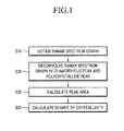
- FIG. 1 is a flowchart of a method of measuring a degree of crystallinity of a polycrystalline silicon substrate according to an embodiment of the invention;
- FIG. 2 is a Raman spectrum graph of a polycrystalline silicon substrate having a degree of crystallinity of 32.8%;
- FIG. 3 is a Raman spectrum graph of a polycrystalline silicon substrate having a degree of crystallinity of 49.7%;
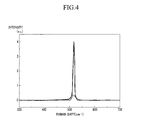
- FIG. 4 is a Raman spectrum graph of a polycrystalline silicon substrate having a degree of crystallinity of 75.5%;
- FIG. 5 is a graph of a PMOS threshold voltage and a full width at half maximum (FWHM) of a Raman spectrum graph according to a degree of crystallinity;
- FIG. 6 is a graph of an ID-Vg characteristic of the polycrystalline silicon substrate having the degree of crystallinity of 32.8%;
- FIG. 7 is a graph of an ID-Vg characteristic of the polycrystalline silicon substrate having the degree of crystallinity of 49.7%;
- FIG. 8 is a graph of an ID-Vg characteristic of the polycrystalline silicon substrate having the degree of crystallinity of 75.5%; and
- FIG. 9 is a flowchart of a method of fabricating an organic light emitting display according to an embodiment of the invention.
- As shown in FIG. 1, a method of measuring the degree of crystallinity of the polycrystalline silicon substrate according to a first embodiment of the invention comprises obtaining a Raman spectrum graph by irradiating the polycrystalline silicon substrate with monochromatic light, such as a laser beam or any other suitable monochromatic light, at block S10; deconvolving the Raman spectrum graph into an amorphous peak and a polycrystalline peak at block S20; calculating an area of the amorphous peak and an area of the polycrystalline peak from data obtained during the deconvolving of the Raman spectrum graph at block S30; and calculating the degree of crystallinity of the polycrystalline silicon substrate using the calculated area of the amorphous peak and the area of the polycrystalline peak according to the following
Formula 1 at block S40:
- The amorphous peak has a centre at 480 cm-1, and the polycrystalline peak has a centre at 517 cm-1.
- FIGS. 2 to 4 are Raman spectrum graphs of polycrystalline silicon substrates having different degrees of crystallinity. As can be seen from FIGS. 2 to 4, each of these Raman spectrum graphs has a different FWHM.
- Using the aforementioned method, the degree of crystallinity is measured to be 32.8% from the Raman spectrum graph of FIG. 2, the degree of crystallinity is measured to be 49.7% from the Raman spectrum graph of FIG. 3, and the degree of crystallinity is measured to be 75.5% from the Raman spectrum graph of FIG. 4.
- FIG. 5 is a graph of a PMOS threshold voltage and a full width at half maximum (FWHM) of a Raman spectrum graph according to a degree of crystallinity of the polycrystalline substrate. As can be seen from FIG. 5, as the degree of crystallinity increases, the threshold voltages become less dispersed. However, the FWHM tends to increase as the degree of crystallinity increases.
- As described above, there is an apparent correlation between the dispersion of the threshold voltage of the polycrystalline silicon substrate and the degree of crystallinity as measured by the method of measuring the degree of crystallinity according to an example embodiment of the invention.
- FIG. 6 is a graph of an ID-Vg characteristic of the polycrystalline silicon substrate having a degree of crystallinity of 32.8%, FIG. 7 is a graph of an ID-Vg characteristic of the polycrystalline silicon substrate having a degree of crystallinity of 49.7%, and FIG. 8 is a graph of an ID-Vg characteristic of the polycrystalline silicon substrate having a degree of crystallinity of 75.5%.
- As can be seen from FIGS. 6 to 8, as the degree of crystallinity calculated using
Formula 1 increases, that is, when moving from FIG. 6 to FIG. 8, a subthreshold slope decreases, and a kink effect decreases. - This means that a polycrystalline silicon substrate having excellent electrical characteristics such as mobility and threshold voltage dispersion can be obtained.
- A method of fabricating an organic light emitting display according to an embodiment of the invention will now be described.
- As shown in FIG. 9, the method of fabricating the organic light emitting display comprises fabricating a polycrystalline silicon substrate by crystallizing an amorphous silicon substrate at block S100; obtaining a Raman spectrum graph by irradiating the polycrystalline silicon substrate with monochromatic light, such as a laser beam or any other suitable monochromatic light, at block S200; examining a degree of crystallinity of the polycrystalline silicon substrate based on the Raman spectrum graph at block S300; and fabricating a thin film transistor at block S400.
- The fabricating of the polycrystalline silicon substrate (S100) may be performed using a solid phase crystallization (SPC) method, an excimer laser annealing (ELA) method, a metal induced crystallization (MIC) method, a metal induced lateral crystallization (MILC) method, or a sequential lateral solidification (SLS) method.
- The SPC method is a method of crystallizing the amorphous silicon substrate by using a high temperature heat treatment.
- The ELA method is a method in which an upper portion of the amorphous silicon substrate is instantaneously melted and recrystallized by irradiating the amorphous silicon substrate with an excimer laser beam.
- The MIC method is a method in which a metal catalyst is coated on the amorphous silicon substrate using a sputtering method or a spin coating method to induce crystallization at a low temperature.
- The MILC method is a method in which metal seeds are deposited on source and drain regions of the amorphous silicon substrate, and crystallization proceeds laterally in the amorphous silicon substrate away from the metal seeds at a low temperature.
- The SLS method is a method in which the amorphous silicon substrate is irradiated with a laser beam two or more times to laterally grow silicon crystal grains to crystallize the amorphous silicon substrate.
- The polycrystalline silicon substrate that is crystallized using any of the aforementioned methods is examined during the examination of the degree of crystallinity using the method of measuring the degree of crystallinity of the polycrystalline silicon substrate according to an embodiment of the invention.
- Specifically, a Raman spectrum graph is obtained by irradiating the polycrystalline silicon substrate with monochromatic light, such as a laser beam or any other suitable monochromatic light, at block S200; and the degree of crystallinity of the polycrystalline silicon substrate is examined using the method of measuring the degree of crystallinity according to an embodiment of the invention at block S300, shown in FIG.9.
- In this case, the thin film transistor used for the organic light emitting display is fabricated using the polycrystalline silicon substrate having a degree of crystallinity that is 70% or more at block S400.
- In an active matrix organic light emitting display, the threshold voltage dispersion causing non-homogeneity of luminance is more important than the absolute value of an electrical characteristic such as mobility or threshold voltage.
- When the threshold voltage dispersion is 1.0V or more, serious non-homogeneity of the luminance occurs even if a circuit for compensating for the threshold voltage dispersion is used.
- Accordingly, the thin film transistor used for the organic light emitting display is fabricated at block S400 using a polycrystalline silicon substrate that is determined to have a degree of crystallinity of 70% or more in the examining of the degree of crystallinity at block S300, while any polycrystalline silicon substrate determined to have a degree of crystallinity of less than 70% is classified as a defective substrate at block S500. However, the invention is not limited to using a degree of crystallinity of 70% as a threshold value at block S300 to determine whether a polycrystalline silicon substrate will be used to fabricate a thin film transistor at block S400, or will be classified as a defective substrate at
block 500, and other degrees of crystallinity may be used as a threshold value atblock 300 depending on the desired characteristics of the thin film transistor to be fabricated. - As described above, in a method of measuring the degree of crystallinity of the polycrystalline silicon substrate and a method of fabricating the organic light emitting display according to the invention, an organic light emitting display having excellent mobility and threshold voltage dispersion characteristics can be provided by using a reliable method of measuring the degree of crystallinity of the polycrystalline silicon substrate.
Claims (11)
- A method of measuring a degree of crystallinity of a polycrystalline silicon substrate, the method comprising:obtaining a Raman spectrum graph by irradiating a polycrystalline silicon substrate with monochromatic light; andcalculating a degree of crystallinity of the polycrystalline silicon substrate from the Raman spectrum graph using the following formula:

- a method according to claim 1, wherein the calculating of the degree of crystallinity of the polycrystalline silicon substrate comprises:deconvolving the Raman spectrum graph into an amorphous peak and a polycrystalline peak;calculating the area of the amorphous peak and the area of the polycrystalline peak from data obtained during the deconvolving of the Rama spectrum graph; andcalculating the degree of crystallinity of the polycrystalline silicon substrate using the calculated area of the amorphous peak and the calculated area of the polycrystalline peak in the formula.
- A method according to claim 2, wherein the amorphous peak has a center at 480 cm-1, and the polycrystalline peak has a center at 517 cm-1.
- A method according to any preceding claim, wherein the monochromatic light is a laser beam.
- A method of fabricating an organic light emitting display, the method comprising:fabricating a polycrystalline silicon substrate by crystallizing an amorphous silicon substrate;obtaining a Raman spectrum graph by irradiating the polycrystalline silicon substrate with monochromatic light;examining a degree of crystallinity of the polycrystalline silicon substrate based on the Raman spectrum graph by using the following formula:
 fabricating a thin film transistor using the polycrystalline silicon substrate depending on a result of the examining of the degree of crystallinity of the polycrystalline silicon substrate.
 - A method according to claim 5, wherein the fabricating of the thin film transistor using the polycrystalline silicon substrate is performed only if the degree of crystallinity of the polycrystalline silicon substrate is determined to be 70% or more in the examining of the degree of crystallinity of the polycrystalline silicon substrate.
- A method according to claim 5 or 6, wherein the examining of the degree of crystallinity of the polycrystalline silicon substrate comprises:deconvolving the Raman spectrum graph into an amorphous peak and a polycrystalline peak;calculating an area of the amorphous peak and an area of the polycrystalline peak from the data obtained during the deconvolving of the Raman spectrum graph; andcalculating the degree of crystallinity using the calculated area of the amorphous peak and the calculated area of the polycrystalline peak in the formula.
- A method according to claim 7, wherein the amorphous peak has a center at 480 cm-1, and the polycrystalline peak has a center at 517 cm-1.
- A method according to one of claims 5 to 8, wherein the fabricating of the polycrystalline silicon substrate comprises crystallizing the amorphous silicon substrate using a solid phase crystallization (SPC) method, an excimer laser annealing (ELA) method, a metal induced crystallization (MIC) method, a metal induced lateral crystallization (MILC) method, or a sequential lateral solidification (SLS) method.
- A method according to one of claims 5 to 9, wherein the monochromatic light is a laser beam.
- An organic light emitting display comprising a polycrystalline silicon substrate having a degree of crystallinity that is 70% or more as determined from a Raman spectrum graph using the following formula:

Applications Claiming Priority (1)
| Application Number | Priority Date | Filing Date | Title |
|---|---|---|---|
| KR1020060093435A KR100786873B1 (en) | 2006-09-26 | 2006-09-26 | Method for measuring crystallinity of polycrystalline silicon substrate, method of manufacturing organic light emitting display device using same and organic light emitting display device |
Publications (2)
| Publication Number | Publication Date |
|---|---|
| EP1906173A2 true EP1906173A2 (en) | 2008-04-02 |
| EP1906173A3 EP1906173A3 (en) | 2008-11-05 |
Family
ID=38962058
Family Applications (1)
| Application Number | Title | Priority Date | Filing Date |
|---|---|---|---|
| EP06256561A Withdrawn EP1906173A3 (en) | 2006-09-26 | 2006-12-22 | Method of measuring degree of crystallinity of polycrystalline silicon substrate, method of fabricating organic light emitting display using the same, and organic light emitting display fabricated using the same |
Country Status (5)
| Country | Link |
|---|---|
| US (1) | US7964417B2 (en) |
| EP (1) | EP1906173A3 (en) |
| JP (1) | JP2008085279A (en) |
| KR (1) | KR100786873B1 (en) |
| CN (1) | CN101153847A (en) |
Families Citing this family (16)
| Publication number | Priority date | Publication date | Assignee | Title |
|---|---|---|---|---|
| KR101009429B1 (en) * | 2008-04-23 | 2011-01-19 | 주식회사 엔씰텍 | Polycrystalline silicon film, thin film transistor comprising same, and method for manufacturing same |
| JP5440039B2 (en) * | 2009-09-04 | 2014-03-12 | ソニー株式会社 | Semiconductor device manufacturing method, semiconductor inspection apparatus, and crystallinity inspection method |
| US20120252192A1 (en) * | 2011-07-08 | 2012-10-04 | Trustees Of Dartmouth College | Method of growing heteroepitaxial single crystal or large grained semiconductor films on glass substrates and devices thereon |
| CN102866142A (en) * | 2011-07-08 | 2013-01-09 | 中国蓝星(集团)股份有限公司 | Method for measuring crystallinity differential value of inner layer and outer layer of carbon fiber |
| KR102105075B1 (en) * | 2013-05-02 | 2020-04-28 | 삼성디스플레이 주식회사 | Method and system for mornitoring of an amorphous silicon thin filim crystallization, and method of manufacturing thin film transistor using the mehtod and system |
| CN103323444A (en) * | 2013-05-27 | 2013-09-25 | 江苏大学 | Method for discriminating disorder degree of polysilicon film |
| CN104949959A (en) * | 2015-07-12 | 2015-09-30 | 北京工业大学 | Quick preparing method for large-area surface Raman spectrum enhancing monocrystalline silicon substrate |
| JP6100745B2 (en) * | 2014-10-01 | 2017-03-22 | ユー・ディー・シー アイルランド リミテッド | Organic electroluminescence device |
| CN104764731B (en) * | 2015-04-01 | 2018-01-16 | 广西科技大学 | A kind of method of Raman spectrum on-line monitoring polyurethane prepolymer NCO content |
| KR102659810B1 (en) * | 2015-09-11 | 2024-04-23 | 삼성디스플레이 주식회사 | Crystallization measure apparatus and method of the same measure |
| CN106057701B (en) * | 2016-08-08 | 2019-02-19 | 武汉华星光电技术有限公司 | Polysilicon grain size measuring device and polysilicon grain size measuring method |
| JP7164110B2 (en) * | 2018-09-28 | 2022-11-01 | 三菱重工業株式会社 | Crystallinity measuring device, resin-containing material manufacturing device, crystallinity measuring method, and resin-containing material manufacturing method |
| JP7332144B2 (en) * | 2019-06-13 | 2023-08-23 | 株式会社ブイ・テクノロジー | LASER MODIFICATION METHOD, LASER MODIFICATION DEVICE |
| CN110274900B (en) * | 2019-07-11 | 2021-07-30 | 长春工业大学 | A monitoring method and system for in situ real-time characterization of the internal interface of a solar cell |
| JP7178710B2 (en) | 2019-07-11 | 2022-11-28 | 株式会社ブイ・テクノロジー | LASER MODIFICATION METHOD, LASER MODIFICATION DEVICE |
| KR102957184B1 (en) | 2020-08-14 | 2026-04-24 | 삼성디스플레이 주식회사 | Apparatus and method for manufacturing a display device |
Family Cites Families (13)
| Publication number | Priority date | Publication date | Assignee | Title |
|---|---|---|---|---|
| JPS62145775A (en) | 1985-12-20 | 1987-06-29 | Hitachi Ltd | Thin film semiconductor device and its manufacturing method |
| JP3491903B2 (en) * | 1990-05-18 | 2004-02-03 | セイコーエプソン株式会社 | Method for manufacturing thin film semiconductor device |
| US5455673A (en) | 1994-05-27 | 1995-10-03 | Eastman Chemical Company | Apparatus and method for measuring and applying a convolution function to produce a standard Raman spectrum |
| JP3305592B2 (en) | 1996-09-30 | 2002-07-22 | シャープ株式会社 | Method for managing quality of crystalline semiconductor film, computer software for managing quality of crystalline semiconductor film, crystalline silicon film, semiconductor device, and thin film transistor |
| US6228693B1 (en) * | 1998-06-05 | 2001-05-08 | Sharp Laboratories Of America, Inc. | Selected site, metal-induced, continuous crystallization method |
| JP2002009012A (en) | 2000-06-21 | 2002-01-11 | Toshiba Corp | Manufacturing method of liquid crystal display device and laser annealing device |
| JP2002231631A (en) | 2001-02-05 | 2002-08-16 | Semiconductor Energy Lab Co Ltd | Semiconductor device, method of manufacturing the same, and semiconductor manufacturing apparatus |
| US7091110B2 (en) | 2002-06-12 | 2006-08-15 | Semiconductor Energy Laboratory Co., Ltd. | Method of manufacturing a semiconductor device by gettering using a anti-diffusion layer |
| KR20050054788A (en) | 2003-12-06 | 2005-06-10 | 삼성전자주식회사 | Fabrication method of poly-crystalline si thin film and transistor thereby |
| KR100569118B1 (en) | 2004-01-20 | 2006-04-10 | 진 장 | Amorphous Silicon Crystallization Apparatus and Crystallization Method of Large Area Amorphous Silicon |
| KR100573144B1 (en) | 2004-05-04 | 2006-04-24 | 삼성에스디아이 주식회사 | Method for crystallizing a semiconductor active layer, a semiconductor active layer thereby, and a flat panel display device having the same |
| KR100544143B1 (en) | 2004-05-21 | 2006-01-23 | 삼성에스디아이 주식회사 | Method for manufacturing thin film transistor, thin film transistor and flat panel display device having same |
| JP2006066607A (en) | 2004-08-26 | 2006-03-09 | Sumitomo Heavy Ind Ltd | Crystallinity-measuring method for silicon film, and manufacturing method for semiconductor device |
-
2006
- 2006-09-26 KR KR1020060093435A patent/KR100786873B1/en active Active
- 2006-10-11 JP JP2006277283A patent/JP2008085279A/en active Pending
- 2006-11-06 US US11/593,090 patent/US7964417B2/en active Active
- 2006-11-28 CN CNA2006101628780A patent/CN101153847A/en active Pending
- 2006-12-22 EP EP06256561A patent/EP1906173A3/en not_active Withdrawn
Also Published As
| Publication number | Publication date |
|---|---|
| JP2008085279A (en) | 2008-04-10 |
| EP1906173A3 (en) | 2008-11-05 |
| KR100786873B1 (en) | 2007-12-20 |
| US7964417B2 (en) | 2011-06-21 |
| US20080121891A1 (en) | 2008-05-29 |
| CN101153847A (en) | 2008-04-02 |
Similar Documents
| Publication | Publication Date | Title |
|---|---|---|
| US7964417B2 (en) | Method of measuring degree of crystallinity of polycrystalline silicon substrate, method of fabricating organic light emitting display using the same, and organic light emitting display fabricated using the same | |
| US7560321B2 (en) | Crystallization method, thin film transistor manufacturing method, thin film transistor, display, and semiconductor device | |
| US6218198B1 (en) | Method and apparatus for evaluating semiconductor film, and method for producing the semiconductor film | |
| US9257288B2 (en) | Method and system for monitoring crystallization of amorphous silicon thin film, and method of manufacturing thin film transistor by using the method and system | |
| US8623746B2 (en) | Polysilicon layer, method of preparing the polysilicon layer, thin film transistor using the polysilicon layer, and organic light emitting display device including the thin film transistor | |
| US20150249159A1 (en) | Thin film transistor | |
| Crowder et al. | Parametric investigation of SLS-processed poly-silicon thin films for TFT applications | |
| US8009345B2 (en) | Crystallization apparatus, crystallization method, device, and light modulation element | |
| US20050017239A1 (en) | Test element group, method of manufacturing a test element group, method of testing a semiconductor device, and semiconductor device | |
| JP2000114174A (en) | Method for manufacturing semiconductor film, method for manufacturing thin film transistor, active matrix substrate, and annealing apparatus | |
| JP6010809B2 (en) | Manufacturing method of semiconductor device | |
| JP4116141B2 (en) | Method for manufacturing crystalline silicon film | |
| JP2003282441A (en) | Method for manufacturing semiconductor crystal layer, semiconductor substrate, and liquid crystal display panel | |
| JP4568000B2 (en) | Manufacturing method of semiconductor thin film | |
| US20120256185A1 (en) | Semiconductor device and process for production thereof, and display device | |
| US20110220892A1 (en) | Semiconductor device and method for manufacturing the same | |
| Shetty et al. | Formation and characterization of silicon films on flexible polymer substrates | |
| US7449377B2 (en) | Method of fabricating poly silicon layer | |
| US7205033B2 (en) | Method for forming polycrystalline silicon film of polycrystalline silicon TFT | |
| US6787434B1 (en) | Method of fabricating polysilicon film by nickel/copper induced lateral crystallization | |
| KR20050078191A (en) | Manufacturing method of semiconductor film and image display device | |
| Hou et al. | Effects of Tensile Stress on Growth of Ni–Metal-Induced Lateral Crystallization of Amorphous Silicon | |
| Pier et al. | Excimer laser crystallization of microcrystalline silicon for TFTs on flexible substrate | |
| Kim et al. | Growth of large-grain poly-Si by FE-SMC | |
| Lee et al. | Influences of directional crystallization using field aided lateral crystallization on the electrical characteristics of poly-Si thin film transistors |
Legal Events
| Date | Code | Title | Description |
|---|---|---|---|
| PUAI | Public reference made under article 153(3) epc to a published international application that has entered the european phase |
Free format text: ORIGINAL CODE: 0009012 |
|
| 17P | Request for examination filed |
Effective date: 20070110 |
|
| AK | Designated contracting states |
Kind code of ref document: A2 Designated state(s): AT BE BG CH CY CZ DE DK EE ES FI FR GB GR HU IE IS IT LI LT LU LV MC NL PL PT RO SE SI SK TR |
|
| AX | Request for extension of the european patent |
Extension state: AL BA HR MK YU |
|
| PUAL | Search report despatched |
Free format text: ORIGINAL CODE: 0009013 |
|
| AK | Designated contracting states |
Kind code of ref document: A3 Designated state(s): AT BE BG CH CY CZ DE DK EE ES FI FR GB GR HU IE IS IT LI LT LU LV MC NL PL PT RO SE SI SK TR |
|
| AX | Request for extension of the european patent |
Extension state: AL BA HR MK RS |
|
| RAP1 | Party data changed (applicant data changed or rights of an application transferred) |
Owner name: SAMSUNG MOBILE DISPLAY CO., LTD. |
|
| AKX | Designation fees paid |
Designated state(s): DE FR GB |
|
| 17Q | First examination report despatched |
Effective date: 20090630 |
|
| STAA | Information on the status of an ep patent application or granted ep patent |
Free format text: STATUS: THE APPLICATION IS DEEMED TO BE WITHDRAWN |
|
| 18D | Application deemed to be withdrawn |
Effective date: 20100112 |