EP1903401A2 - Self erasing photoreceptor containing an optically transparent, conductive electroluminescent carbon nanotube ground plane - Google Patents
Self erasing photoreceptor containing an optically transparent, conductive electroluminescent carbon nanotube ground plane Download PDFInfo
- Publication number
- EP1903401A2 EP1903401A2 EP20070117033 EP07117033A EP1903401A2 EP 1903401 A2 EP1903401 A2 EP 1903401A2 EP 20070117033 EP20070117033 EP 20070117033 EP 07117033 A EP07117033 A EP 07117033A EP 1903401 A2 EP1903401 A2 EP 1903401A2
- Authority
- EP
- European Patent Office
- Prior art keywords
- electrophotographic photoreceptor
- conductive layer
- contact
- photoreceptor according
- electroluminescent
- Prior art date
- Legal status (The legal status is an assumption and is not a legal conclusion. Google has not performed a legal analysis and makes no representation as to the accuracy of the status listed.)
- Granted
Links
Images

Classifications
-
- G—PHYSICS
- G03—PHOTOGRAPHY; CINEMATOGRAPHY; ANALOGOUS TECHNIQUES USING WAVES OTHER THAN OPTICAL WAVES; ELECTROGRAPHY; HOLOGRAPHY
- G03G—ELECTROGRAPHY; ELECTROPHOTOGRAPHY; MAGNETOGRAPHY
- G03G5/00—Recording-members for original recording by exposure, e.g. to light, to heat or to electrons; Manufacture thereof; Selection of materials therefor
- G03G5/10—Bases for charge-receiving or other layers
- G03G5/102—Bases for charge-receiving or other layers consisting of or comprising metals
-
- G—PHYSICS
- G03—PHOTOGRAPHY; CINEMATOGRAPHY; ANALOGOUS TECHNIQUES USING WAVES OTHER THAN OPTICAL WAVES; ELECTROGRAPHY; HOLOGRAPHY
- G03G—ELECTROGRAPHY; ELECTROPHOTOGRAPHY; MAGNETOGRAPHY
- G03G5/00—Recording-members for original recording by exposure, e.g. to light, to heat or to electrons; Manufacture thereof; Selection of materials therefor
- G03G5/10—Bases for charge-receiving or other layers
-
- G—PHYSICS
- G03—PHOTOGRAPHY; CINEMATOGRAPHY; ANALOGOUS TECHNIQUES USING WAVES OTHER THAN OPTICAL WAVES; ELECTROGRAPHY; HOLOGRAPHY
- G03G—ELECTROGRAPHY; ELECTROPHOTOGRAPHY; MAGNETOGRAPHY
- G03G5/00—Recording-members for original recording by exposure, e.g. to light, to heat or to electrons; Manufacture thereof; Selection of materials therefor
- G03G5/10—Bases for charge-receiving or other layers
- G03G5/104—Bases for charge-receiving or other layers comprising inorganic material other than metals, e.g. salts, oxides, carbon
-
- G—PHYSICS
- G03—PHOTOGRAPHY; CINEMATOGRAPHY; ANALOGOUS TECHNIQUES USING WAVES OTHER THAN OPTICAL WAVES; ELECTROGRAPHY; HOLOGRAPHY
- G03G—ELECTROGRAPHY; ELECTROPHOTOGRAPHY; MAGNETOGRAPHY
- G03G5/00—Recording-members for original recording by exposure, e.g. to light, to heat or to electrons; Manufacture thereof; Selection of materials therefor
- G03G5/10—Bases for charge-receiving or other layers
- G03G5/105—Bases for charge-receiving or other layers comprising electroconductive macromolecular compounds
Definitions
- the subject matter of this invention relates to photoreceptors. More particularly, the subject matter of this invention relates to self erasing photoreceptors containing an optically transparent, conductive electroluminescent carbon nanotube ground plane for use in an electrophotographic apparatus.
- ground plane resistivity i.e. sheet resistivity
- metals such as Al, Ti, Zr.
- belt photoreceptors that erase by illuminating through the ground plane, i.e. by "rear erase” require further increase in erase lamp intensity.
- the use of an anti-curl back coat on a belt photoreceptor further increases the need for higher intensity erase illumination because over time its surface becomes rather scratched and abraded. Consequently some of the illumination is scattered or diffracted and is prevented from reaching the charge generator layer.
- the electrophotographic photoreceptor can include a conductive layer including a plurality of electroluminescent nanomaterials.
- the electrophotographic photoreceptor can also include a first contact electrically connected to a first edge of the conductive layer and an electrical ground and a second contact electrically connected to a second edge of the conductive layer and a D.C. power supply.
- the electrophotographic photoreceptor can have the D.C. power supply configured to supply a lateral voltage bias at the second contact to generate a localized electroluminescence across the conductive layer and deliver an erase illumination from within the electrophotographic photoreceptor.
- the electrophotographic photoreceptor can also include a photosensitive layer disposed over the conductive layer, wherein the photosensitive layer includes a charge generation material and a charge transport material. Moreover, the electrophotographic photoreceptor can have the D.C. power supply configured to supply a lateral voltage bias at the second contact to generate a localized electroluminescence across the conductive layer and deliver an erase illumination from within the electrophotographic photoreceptor.
- the image forming apparatus can include an electrophotographic photoreceptor, wherein the electrophotographic photoreceptor includes a conductive layer, and wherein the conductive layer includes a plurality of electroluminescent nanomaterials.
- the image forming apparatus can also include a charging station for uniformly charging the electrophotographic photoreceptor and an imaging station for forming a latent image on the electrophotographic photoreceptor.
- the image forming apparatus can further include a development subsystem for converting the latent image to a visible image on the electrophotographic photoreceptor and a transfer station for transferring and fixing the visible image onto a media.
- the image forming apparatus can have the conductive layer with a first edge and a second edge opposite the first edge, wherein the first edge has a first contact connected to an electrical ground and the second edge has a second contact connected to a D.C. power supply. Moreover, the image forming apparatus can have the D.C. power supply configured to supply a lateral voltage bias at the second contact to generate a localized electroluminescence across the conductive layer and deliver an erase illumination from within the electrophotographic photoreceptor.
- the method can include providing an electrophotographic photoreceptor, wherein the electrophotographic photoreceptor includes a conductive layer, and wherein the conductive layer includes a plurality of electroluminescent nanomaterials.
- the method can also include providing an imaging station for forming a latent image on the electrophotographic photoreceptor and providing a development subsystem for converting the latent image to a visible image on the electrophotographic photoreceptor.
- the method can further include providing a transfer station for transferring and fixing the visible image onto a media and applying a bias voltage laterally across the conductive layer to make the conductive layer glow laterally and deliver erase illumination from within the electrophotographic photoreceptor.
- FIG. 1 is a schematic illustration of an exemplary electrophotographic photoreceptor according to various embodiments of the present teachings.
- FIG. 2 illustrates side view of an exemplary electrophotographic photoreceptor in accordance with the present teachings.
- FIG. 3 is a schematic illustration of another exemplary electrophotographic photoreceptor in accordance with the present teachings.
- FIG. 4 illustrates an exemplary image forming apparatus according to various embodiments of the present teachings.
- FIG. 5 is a schematic illustration of an exemplary conductive layer comprising a plurality of carbon nanotubes according to various embodiments of the present teachings.
- electrostatic photoreceptor is used interchangeably herein with “image receptor” and “photoreceptor”.
- conductive layer is used interchangeably herein with “ground plane”, “conductive ground plane”, “electroluminescent conductive layer”, “optically transparent conductive ground plane”, etc.
- nanomaterial is used herein to refer to any material having at least one dimension in the nanoscale range of about 0.1 nm to about 100 nm, including but not limited to, for example, nanotubes, nanofibers, nanotorus, etc.
- nanomaterials such as carbon nanotubes
- a length of the carbon nanotube can be several millimeters
- similarly carbon nanotube sheets need to have only thickness in the nanoscale region, the width and length of the carbon nanotube sheet can be in the nanoscale, microscopic, or macroscopic range.
- Self erasing photoreceptor including a conductive ground plane including a plurality of electroluminescent nanomaterials can provide several advantages.
- the internal erase illumination can provide optical advantage of minimal required erase illumination because of proximity to the charge generating layer.
- the fewer internal reflections can also minimize the required erase electroluminescent illumination.
- internally generated illumination can not be diffracted by the scratched rear surface of a belt photoreceptor which occurs over time.
- FIG. 1 is a schematic illustration of an exemplary electrophotographic photoreceptor 100 according to various embodiments.
- the electrophotographic photoreceptor 100 can include a conductive layer 110 including a plurality of electroluminescent nanomaterials.
- the electrophotographic photoreceptor 100 can include a first contact 122 electrically connected to a first edge 112 of the conductive layer 110 and an electrical ground 120 and a second contact 124 electrically connected to a second edge 114 of the conductive layer 110 and a D.C. power supply 125.
- the electrophotographic photoreceptor 100 can also include a biasing contact 128 proximate to the second contact 124, connected to a D.C. power supply 125 to apply a voltage bias laterally across the conductive layer 110.
- the electrophotographic photoreceptor 100 can also include a photosensitive layer 130 disposed over the conductive layer 110 as shown in FIG. 2.
- the photosensitive layer 130 can include a charge generation material and a charge transport material.
- the electrophotographic photoreceptor 100 can also include a protective hard coat layer over the photosensitive layer 130.
- the hard coat layer can have thickness from about 1 to about 5 microns and typically from about 2 to about 4 microns.
- the plurality of electroluminescent nanomaterials can include a plurality of carbon nanotubes.
- the conductive layer 110 can include carbon nanotube composite, including but not limited to carbon nanotube polymer composite, epoxy based carbon nanotube composite, and carbon nanotube filled resin.
- FIG. 5 is a schematic illustration of an exemplary conductive layer 510 including a plurality of carbon nanotubes 595 in a carbon nanotube composite 590.
- the conductive layer 110 can have a thickness from about 0.01 ⁇ m to about 1.5 ⁇ m and in some cases from about 0.05 ⁇ m to about 1 ⁇ m.
- the concentration of carbon nanotube in the carbon nanotube composite can be from about 0.01 wt % to about 10 wt % and in some cases from about 0.05 wt % to about 5 wt %.
- the carbon nanotubes can be SWNT (single walled carbon nanotubes) or MWNT (multi walled carbon nanotubes).
- Carbon nanotubes can have diameter from about 1 nm to about 100 nm and in some cases from about 5 nm to about 50 nm and can have length from about 50 nm to about 5 mm and in some cases from about 100 nm to about 1 mm.
- the conductive layer 110 can include a layer of at least one carbon nanotube sheet on a substrate.
- the carbon nanotube sheet can have thickness in the range of about 50 nm to about 500 nm.
- the conductive layer 110 can include carbon nanotube sheet supported by one or more optically transparent supporting layers.
- optically transparent supporting layers include polyethylene, oriented Mylar sheet, polycarbonate and other synthetic polymeric materials applied as an anti-curl layer to the electrophotographic photoreceptor 100.
- the conductive layer 110 including carbon nanotubes can have several advantages over conventional metal films used for conductive ground planes.
- Carbon nanotubes exhibit many desirable properties for conductive ground plane such as high optical transparency with electronic conductivity, are non-oxidizable, flexible, and have high tensile strength.
- Carbon nanotubes can also exhibit electroluminescence in the visible and into the infrared spectrum, the wavelength range used for erasing in a photoreceptor.
- These un-optimized carbon nanotube sheets can exceed steel and carbon fiber material such as Kevlar in gravimetric strength.
- micron thick carbon nanotube sheets can support liquid droplets 50,000 times their own weight.
- carbon nanotube sheet can act as electrodes that can be reversibly deformed without losing electrical conductivity. Further, as electrodes, the carbon nanotube sheets can exhibit very little change in conductivity over a very wide temperature range.
- the electrophotographic photoreceptor 100 can have the D.C. power supply 125 configured to supply a lateral voltage bias at the second contact 124 to generate a localized electroluminescence 140 across the conductive layer 110 and deliver an erase illumination from within the electrophotographic photoreceptor 100.
- the localized electroluminescence 140 across the conductive layer 110 can be from about 0.5 mm to about 10 cm and in some cases from about 1 mm to about 5 cm in width.
- the lateral voltage bias at the second contact 124 to generate electroluminescence 140 can be from about 20 V to about 80 V and in some cases from about 30 V to about 60 V.
- the lateral bias can be applied using a biasing contact 128, where the biasing contact 128 can be for example a roller, a brush, a sliding contact such as a metal or carbon clip, etc.
- the second contact 124 can be a strip of semiconductive material.
- the second contact 124 can have a sheet resistance of about 10 4 to about 10 6 ohm/sq.
- Suitable contact 124 can be any type of carbon particle filled resin or polymer where the concentration of carbon is adjusted to provide the desired resistivity.
- Non limiting examples of the first contact 122 include stainless steel roller, metal or carbon particle filled rollers, gold coated base metal (such as aluminum, copper, brass and the like), and a metal (such as aluminum, copper, brass) or carbon filled resin brush.
- the photosensitive layer 130 can include a charge generation material and a charge transport material.
- the photosensitive layer 130 can have thickness from about 5 ⁇ m to about 50 ⁇ m and in some cases from about 15 ⁇ m to about 35 ⁇ m.
- the photosensitive layer 130 can include a charge transport layer disposed over a charge generation layer.
- the photosensitive layer 130 can include a charge generation layer disposed over a charge transport layer.
- the charge generation material and the charge transport material can be dispersed in a common matrix such as polymer or resin.
- Non limiting examples of polymer or resin include polycarbonate, polystyrene, polyvinyl carbazole, and the like.
- the charge generating materials can include organic pigments and organic dyes such as for example hydroxygallium phthalocyanine, vanadyl phthalocyanine, titanyl phthalocyanine, metal-free-pthalocyanines, perylenes such as benzimidazole perylene and congeners, squaraine dyes, pigments, and the like, and mixtures thereof.
- the charge transporting materials can include organic arylamine compounds such as for example, triarylamines including its alkyl, aryl, alkoxy, aryloxy, halogen, amino substituted congeners, arylamine substituted biphenyl and terphenyl, and the like and the mixtures thereof.
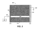
- FIG. 3 is a schematic illustration of another exemplary embodiment of an electrophotographic photoreceptor 300.
- the electrophotographic photoreceptor 300 can include a conductive layer 310 including a plurality of electroluminescent nanomaterial.
- the electrophotographic photoreceptor 300 can include a first contact 322 electrically connected to a first edge 312 of the conductive layer 310 and an electrical ground 320 and a second contact 324 electrically connected to a second edge 314 of the conductive layer 310 and a D.C. power supply 325.
- the electrophotographic photoreceptor 300 can also include a biasing contact 328 proximate to the second contact 324 and connected to the D.C.
- the power supply 325 to apply voltage bias laterally across the conductive layer 310 to generate a localized electroluminescence 340 across the conductive layer 310 and deliver an erase illumination from within the electrophotographic photoreceptor 300.
- the localized electroluminescence 340 across the conductive layer 310 can be from about 0.5 mm to about 10 cm and in some cases from about 1 mm to about 5 cm in width.
- the lateral voltage bias at the second contact 324 to generate electroluminescence 340 can be from about 20 V to about 80 V and in some cases from about 30 V to about 60 V.
- the second contact 324 can include a plurality of segmented staggered contact arrays 324.
- the segmented staggered contact arrays 324 can include at least two columns, a first column spatially separated from a second column, wherein each column includes segmented contacts spatially separated from each other.
- the first and the second column can be placed vertically offset to each other such that the segments of first column are vertically offset to the segments of the second column.
- the segmentation in the segmented staggered contact array 324 can prevent the entire conductive layer 310 from being energized by the voltage bias. Further, the staggering in the segmented staggered contact array 324 due to the vertical offset can ensure that all areas of the conductive layer 110 will emit light and produce erase illumination and hence complete erasure of the residual latent image.
- the first contact 322 and the second contact 324 can be made of the same conductive materials.
- the first contact 322 and the second contact 324 can be at least one of stainless steel rollers, metal or carbon particle filled rollers, gold coated base metal (such as aluminum, copper, brass and the like), and a metal (such as aluminum, copper, brass) or carbon filled resin brush contact.
- the electrophotographic receptor 300 can also include a photosensitive layer 130 disposed over the conductive layer 110 as shown in FIG. 2.
- the electrophotographic receptor 300 can also include a protective hard coat layer over the photosensitive layer 130.
- the electrophotographic receptor 100, 300 can be a belt photoreceptor or a drum photoreceptor.
- current drum photoreceptors are based on a conductive drum substrate.
- the conductive substrate of the drum photoreceptor can be anodized in order not to short out the lateral voltage bias applied to the conductive layer 110.
- a plastic substrate can be used in the drum photoreceptor, and electrophotographic photoreceptor 100, 300 can be disposed over the plastic substrate. Further, to save space in drum photoreceptor, the location of the light emission can be coincident with the cleaning sub-system.
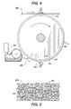
- FIG. 4 illustrates an exemplary image forming apparatus 400.
- the exemplary image forming apparatus can include an electrophotographic photoreceptor 401.
- the electrophotographic receptor 401 can include a conductive layer 410 and a photosensitive layer 430 disposed over the conductive layer 410.
- the conductive layer 410 can include a plurality of electroluminescent nanomaterials.
- the image forming apparatus 400 can have a charging station 440 for uniformly charging the electrophotographic photoreceptor 401.
- the elcetrophotographic photoreceptor 401 can be a drum photoreceptor as shown in FIG. 4 or a belt photoreceptor (not shown).
- the image forming apparatus 400 can also include an imaging station 450 where an original document (not shown) can be exposed to a light source (also not shown) for forming a latent image on the electrophotographic photoreceptor 401.
- the image forming apparatus 400 can further include a development subsystem 460 for converting the latent image to a visible image on the electrophotographic photoreceptor 401 and a transfer station 470 for transferring and fixing the visible image onto a paper or other media.
- the conductive layer 410 can have a first edge 112 and a second edge 114 opposite the first edge 112, wherein the first edge 112 has a first contact 122 connected to an electrical ground 120 and the second edge 114 has a second contact 124 connected to a D.C.
- the D.C. power supply 125 can be configured to supply the voltage bias at the second contact 124 to generate a localized electroluminescence 140 across the conductive layer 410 and deliver an erase illumination from within the electrophotographic photoreceptor 401.
- the erase illumination can be from about 0.5 mm to about 10 cm and in some cases from about 1 mm to about 5 mm.
- the second contact 124 can be a strip of semiconductive material as shown in FIG. 1, with a sheet resistance of about 10 4 to about 10 6 ohm/sq.
- the second contact 124 can include a segmented array of contacts 324 as shown in FIG.
- the second contact can include a segmented staggered array of contacts 324, wherein the staggering of contacts can ensure that all areas of the conductive layer will emit light and deliver erase illumination as shown in FIG. 3, and wherein the second contact can be made of the same conductive material as the first contact.
- the method can include providing an electrophotographic photoreceptor 401, wherein the electrophotographic photoreceptor 401 can include a conductive layer 410 including a plurality of electroluminescent nanomaterials and a photosensitive layer 430 disposed over the conductive layer 410.
- the method can also include providing a charging station 440 for uniformly charging the electrophotographic photoreceptor 401.
- the method can further include providing an imaging station 450 where an original document (not shown) can be exposed to a light source (also not shown) for forming a latent image on the electrophotographic photoreceptor 401.
- the method can also include providing a development subsystem 460 for converting the latent image to a visible image on the electrophotographic photoreceptor 401 and a transfer station 470 for transferring and fixing the visible image onto a paper or other media. Furthermore, the method can include applying a bias voltage laterally across the conductive layer 410 to make the conductive layer 410 glow laterally and thereby deliver erase illumination.
- the erase illumination across the conductive layer 410 can be from about 0.5 mm to about 10 cm and in some cases from about 1 mm to about 5 cm in width.
- the plurality of electroluminescent nanomaterials can include a plurality of carbon nanotubes. In other embodiments, the plurality of electroluminescent nanomaterials can include at least one carbon nanotube sheet.
Landscapes
- Physics & Mathematics (AREA)
- General Physics & Mathematics (AREA)
- Spectroscopy & Molecular Physics (AREA)
- Chemical & Material Sciences (AREA)
- Inorganic Chemistry (AREA)
- Photoreceptors In Electrophotography (AREA)
- Electroluminescent Light Sources (AREA)
- Discharging, Photosensitive Material Shape In Electrophotography (AREA)
Abstract
Description
- The subject matter of this invention relates to photoreceptors. More particularly, the subject matter of this invention relates to self erasing photoreceptors containing an optically transparent, conductive electroluminescent carbon nanotube ground plane for use in an electrophotographic apparatus.
- Trends in color xerographic printing include reduced box weight and size, higher process speeds and parallel printing in order to minimize cost, improve productivity and reliability. This has led to a drive for smaller photoreceptors, particularly drum photoreceptors which results in squeezing the space available to the subsystem components disposed around the photoreceptor. In electrophotographic systems, after the transfer of the toner to the paper, the toner is cleaned off the photoreceptor and the photoreceptor is exposed to an erase light to remove the residual latent image. However, long print runs of a single image can lead to variations in optical transparency related to image content. Further conductive ground planes based on strongly reducing metals such as Al, Ti, Zr are gradually converted to their oxides as a result of xerographic cycling. Also, holes traversing the photoreceptor in combination with ambient water electrochemically convert the metals to their insulating oxides resulting in a change in charge acceptance and transparency. Consequently both the erase illumination and ground plane conductivity vary spatially according to image content leading to image ghosts which limits photoreceptor life. Suitable materials for non-electrochemically reactive, optically transparent conductive ground planes are limited. Dispersed carbon particles are not electrochemically reactive but they are unsuitable material for conductive ground plane because of poor optical transparency. Other alternative optically transparent conductive ground planes such as cuprous oxide and conducting polymers including polypyrrole and polyaniline have problems due to relative immaturity of the technology.
- Furthermore, it is difficult to achieve both high optical transparency and low ground plane resistivity (i.e. sheet resistivity) at the same time in either carbon filled or conductive ground planes based on metals such as Al, Ti, Zr. Moreover, belt photoreceptors that erase by illuminating through the ground plane, i.e. by "rear erase" require further increase in erase lamp intensity. In addition, the use of an anti-curl back coat on a belt photoreceptor further increases the need for higher intensity erase illumination because over time its surface becomes rather scratched and abraded. Consequently some of the illumination is scattered or diffracted and is prevented from reaching the charge generator layer.
- Thus, there is a need to overcome these and other problems of the prior art to provide a method and system for internal erase illumination or "self erasing" of the photoreceptor comprising electroluminescent conductive ground plane.
- In accordance with the invention, there is an electrophotographic photoreceptor. The electrophotographic photoreceptor can include a conductive layer including a plurality of electroluminescent nanomaterials. The electrophotographic photoreceptor can also include a first contact electrically connected to a first edge of the conductive layer and an electrical ground and a second contact electrically connected to a second edge of the conductive layer and a D.C. power supply. Furthermore, the electrophotographic photoreceptor can have the D.C. power supply configured to supply a lateral voltage bias at the second contact to generate a localized electroluminescence across the conductive layer and deliver an erase illumination from within the electrophotographic photoreceptor. The electrophotographic photoreceptor can also include a photosensitive layer disposed over the conductive layer, wherein the photosensitive layer includes a charge generation material and a charge transport material. Moreover, the electrophotographic photoreceptor can have the D.C. power supply configured to supply a lateral voltage bias at the second contact to generate a localized electroluminescence across the conductive layer and deliver an erase illumination from within the electrophotographic photoreceptor.
- According to another embodiment of the present teachings, there is an image forming apparatus. The image forming apparatus can include an electrophotographic photoreceptor, wherein the electrophotographic photoreceptor includes a conductive layer, and wherein the conductive layer includes a plurality of electroluminescent nanomaterials. The image forming apparatus can also include a charging station for uniformly charging the electrophotographic photoreceptor and an imaging station for forming a latent image on the electrophotographic photoreceptor. The image forming apparatus can further include a development subsystem for converting the latent image to a visible image on the electrophotographic photoreceptor and a transfer station for transferring and fixing the visible image onto a media. The image forming apparatus can have the conductive layer with a first edge and a second edge opposite the first edge, wherein the first edge has a first contact connected to an electrical ground and the second edge has a second contact connected to a D.C. power supply. Moreover, the image forming apparatus can have the D.C. power supply configured to supply a lateral voltage bias at the second contact to generate a localized electroluminescence across the conductive layer and deliver an erase illumination from within the electrophotographic photoreceptor.
- According to yet another embodiment of the present teachings, there is a method of forming an image. The method can include providing an electrophotographic photoreceptor, wherein the electrophotographic photoreceptor includes a conductive layer, and wherein the conductive layer includes a plurality of electroluminescent nanomaterials. The method can also include providing an imaging station for forming a latent image on the electrophotographic photoreceptor and providing a development subsystem for converting the latent image to a visible image on the electrophotographic photoreceptor. The method can further include providing a transfer station for transferring and fixing the visible image onto a media and applying a bias voltage laterally across the conductive layer to make the conductive layer glow laterally and deliver erase illumination from within the electrophotographic photoreceptor.
- Additional advantages of the embodiments will be set forth in part in the description which follows, and in part will be obvious from the description, or may be learned by practice of the invention. The advantages will be realized and attained by means of the elements and combinations particularly pointed out in the appended claims.
- FIG. 1 is a schematic illustration of an exemplary electrophotographic photoreceptor according to various embodiments of the present teachings.
- FIG. 2 illustrates side view of an exemplary electrophotographic photoreceptor in accordance with the present teachings.
- FIG. 3 is a schematic illustration of another exemplary electrophotographic photoreceptor in accordance with the present teachings.
- FIG. 4 illustrates an exemplary image forming apparatus according to various embodiments of the present teachings.
- FIG. 5 is a schematic illustration of an exemplary conductive layer comprising a plurality of carbon nanotubes according to various embodiments of the present teachings.
- The term "electrophotographic photoreceptor" is used interchangeably herein with "image receptor" and "photoreceptor". The term "conductive layer" is used interchangeably herein with "ground plane", "conductive ground plane", "electroluminescent conductive layer", "optically transparent conductive ground plane", etc. The term "nanomaterial" is used herein to refer to any material having at least one dimension in the nanoscale range of about 0.1 nm to about 100 nm, including but not limited to, for example, nanotubes, nanofibers, nanotorus, etc. Hence, nanomaterials, such as carbon nanotubes, need to have only a diameter in the nanoscale range, but a length of the carbon nanotube can be several millimeters, and similarly carbon nanotube sheets need to have only thickness in the nanoscale region, the width and length of the carbon nanotube sheet can be in the nanoscale, microscopic, or macroscopic range.
- Self erasing photoreceptor including a conductive ground plane including a plurality of electroluminescent nanomaterials can provide several advantages. In some embodiments, the internal erase illumination can provide optical advantage of minimal required erase illumination because of proximity to the charge generating layer. In other embodiments, the fewer internal reflections can also minimize the required erase electroluminescent illumination. Additionally, internally generated illumination can not be diffracted by the scratched rear surface of a belt photoreceptor which occurs over time.
- FIG. 1 is a schematic illustration of an exemplary
electrophotographic photoreceptor 100 according to various embodiments. Theelectrophotographic photoreceptor 100 can include aconductive layer 110 including a plurality of electroluminescent nanomaterials. Theelectrophotographic photoreceptor 100 can include afirst contact 122 electrically connected to afirst edge 112 of theconductive layer 110 and anelectrical ground 120 and asecond contact 124 electrically connected to asecond edge 114 of theconductive layer 110 and aD.C. power supply 125. Theelectrophotographic photoreceptor 100 can also include abiasing contact 128 proximate to thesecond contact 124, connected to aD.C. power supply 125 to apply a voltage bias laterally across theconductive layer 110. Theelectrophotographic photoreceptor 100 can also include aphotosensitive layer 130 disposed over theconductive layer 110 as shown in FIG. 2. Thephotosensitive layer 130 can include a charge generation material and a charge transport material. In some embodiments, theelectrophotographic photoreceptor 100 can also include a protective hard coat layer over thephotosensitive layer 130. The hard coat layer can have thickness from about 1 to about 5 microns and typically from about 2 to about 4 microns. - According to various embodiments, the plurality of electroluminescent nanomaterials can include a plurality of carbon nanotubes. In some embodiments, the
conductive layer 110 can include carbon nanotube composite, including but not limited to carbon nanotube polymer composite, epoxy based carbon nanotube composite, and carbon nanotube filled resin. FIG. 5 is a schematic illustration of an exemplaryconductive layer 510 including a plurality ofcarbon nanotubes 595 in acarbon nanotube composite 590. Theconductive layer 110 can have a thickness from about 0.01 µm to about 1.5 µm and in some cases from about 0.05 µm to about 1 µm. The concentration of carbon nanotube in the carbon nanotube composite can be from about 0.01 wt % to about 10 wt % and in some cases from about 0.05 wt % to about 5 wt %. According to various embodiments, the carbon nanotubes can be SWNT (single walled carbon nanotubes) or MWNT (multi walled carbon nanotubes). Carbon nanotubes can have diameter from about 1 nm to about 100 nm and in some cases from about 5 nm to about 50 nm and can have length from about 50 nm to about 5 mm and in some cases from about 100 nm to about 1 mm. In other embodiments, theconductive layer 110 can include a layer of at least one carbon nanotube sheet on a substrate. The carbon nanotube sheet can have thickness in the range of about 50 nm to about 500 nm. In some embodiments, theconductive layer 110 can include carbon nanotube sheet supported by one or more optically transparent supporting layers. Non limiting examples of optically transparent supporting layers include polyethylene, oriented Mylar sheet, polycarbonate and other synthetic polymeric materials applied as an anti-curl layer to theelectrophotographic photoreceptor 100. - The
conductive layer 110 including carbon nanotubes can have several advantages over conventional metal films used for conductive ground planes. Carbon nanotubes exhibit many desirable properties for conductive ground plane such as high optical transparency with electronic conductivity, are non-oxidizable, flexible, and have high tensile strength. Carbon nanotubes can also exhibit electroluminescence in the visible and into the infrared spectrum, the wavelength range used for erasing in a photoreceptor. These un-optimized carbon nanotube sheets can exceed steel and carbon fiber material such as Kevlar in gravimetric strength. For example, micron thick carbon nanotube sheets can support liquid droplets 50,000 times their own weight. Also, carbon nanotube sheet can act as electrodes that can be reversibly deformed without losing electrical conductivity. Further, as electrodes, the carbon nanotube sheets can exhibit very little change in conductivity over a very wide temperature range. - Referring back to FIG. 1, the
electrophotographic photoreceptor 100 can have theD.C. power supply 125 configured to supply a lateral voltage bias at thesecond contact 124 to generate alocalized electroluminescence 140 across theconductive layer 110 and deliver an erase illumination from within theelectrophotographic photoreceptor 100. Thelocalized electroluminescence 140 across theconductive layer 110 can be from about 0.5 mm to about 10 cm and in some cases from about 1 mm to about 5 cm in width. The lateral voltage bias at thesecond contact 124 to generateelectroluminescence 140 can be from about 20 V to about 80 V and in some cases from about 30 V to about 60 V. In accordance with various embodiments, the lateral bias can be applied using abiasing contact 128, where thebiasing contact 128 can be for example a roller, a brush, a sliding contact such as a metal or carbon clip, etc. In some embodiments, thesecond contact 124 can be a strip of semiconductive material. Thesecond contact 124 can have a sheet resistance of about 104 to about 106 ohm/sq.Suitable contact 124 can be any type of carbon particle filled resin or polymer where the concentration of carbon is adjusted to provide the desired resistivity. Non limiting examples of thefirst contact 122 include stainless steel roller, metal or carbon particle filled rollers, gold coated base metal (such as aluminum, copper, brass and the like), and a metal (such as aluminum, copper, brass) or carbon filled resin brush. - Referring back to FIG. 2, the
photosensitive layer 130 can include a charge generation material and a charge transport material. Thephotosensitive layer 130 can have thickness from about 5 µm to about 50 µm and in some cases from about 15 µm to about 35 µm. In some embodiments, thephotosensitive layer 130 can include a charge transport layer disposed over a charge generation layer. In other embodiments, thephotosensitive layer 130 can include a charge generation layer disposed over a charge transport layer. Yet in some other embodiments, the charge generation material and the charge transport material can be dispersed in a common matrix such as polymer or resin. Non limiting examples of polymer or resin include polycarbonate, polystyrene, polyvinyl carbazole, and the like. The charge generating materials can include organic pigments and organic dyes such as for example hydroxygallium phthalocyanine, vanadyl phthalocyanine, titanyl phthalocyanine, metal-free-pthalocyanines, perylenes such as benzimidazole perylene and congeners, squaraine dyes, pigments, and the like, and mixtures thereof. The charge transporting materials can include organic arylamine compounds such as for example, triarylamines including its alkyl, aryl, alkoxy, aryloxy, halogen, amino substituted congeners, arylamine substituted biphenyl and terphenyl, and the like and the mixtures thereof. - FIG. 3 is a schematic illustration of another exemplary embodiment of an
electrophotographic photoreceptor 300. Theelectrophotographic photoreceptor 300 can include aconductive layer 310 including a plurality of electroluminescent nanomaterial. Theelectrophotographic photoreceptor 300 can include afirst contact 322 electrically connected to afirst edge 312 of theconductive layer 310 and anelectrical ground 320 and asecond contact 324 electrically connected to asecond edge 314 of theconductive layer 310 and aD.C. power supply 325. In some embodiments, theelectrophotographic photoreceptor 300 can also include abiasing contact 328 proximate to thesecond contact 324 and connected to theD.C. power supply 325 to apply voltage bias laterally across theconductive layer 310 to generate alocalized electroluminescence 340 across theconductive layer 310 and deliver an erase illumination from within theelectrophotographic photoreceptor 300. Thelocalized electroluminescence 340 across theconductive layer 310 can be from about 0.5 mm to about 10 cm and in some cases from about 1 mm to about 5 cm in width. The lateral voltage bias at thesecond contact 324 to generateelectroluminescence 340 can be from about 20 V to about 80 V and in some cases from about 30 V to about 60 V. In certain embodiments, thesecond contact 324 can include a plurality of segmentedstaggered contact arrays 324. The segmentedstaggered contact arrays 324 can include at least two columns, a first column spatially separated from a second column, wherein each column includes segmented contacts spatially separated from each other. The first and the second column can be placed vertically offset to each other such that the segments of first column are vertically offset to the segments of the second column. The segmentation in the segmentedstaggered contact array 324 can prevent the entireconductive layer 310 from being energized by the voltage bias. Further, the staggering in the segmentedstaggered contact array 324 due to the vertical offset can ensure that all areas of theconductive layer 110 will emit light and produce erase illumination and hence complete erasure of the residual latent image. According to various embodiments, thefirst contact 322 and thesecond contact 324 can be made of the same conductive materials. In some embodiments, thefirst contact 322 and thesecond contact 324 can be at least one of stainless steel rollers, metal or carbon particle filled rollers, gold coated base metal (such as aluminum, copper, brass and the like), and a metal (such as aluminum, copper, brass) or carbon filled resin brush contact. Theelectrophotographic receptor 300 can also include aphotosensitive layer 130 disposed over theconductive layer 110 as shown in FIG. 2. In various embodiments, theelectrophotographic receptor 300 can also include a protective hard coat layer over thephotosensitive layer 130. - According to various embodiments, the
electrophotographic receptor conductive layer 110. Alternatively, a plastic substrate can be used in the drum photoreceptor, andelectrophotographic photoreceptor - FIG. 4 illustrates an exemplary
image forming apparatus 400. The exemplary image forming apparatus can include anelectrophotographic photoreceptor 401. Theelectrophotographic receptor 401 can include aconductive layer 410 and aphotosensitive layer 430 disposed over theconductive layer 410. Theconductive layer 410 can include a plurality of electroluminescent nanomaterials. Theimage forming apparatus 400 can have a chargingstation 440 for uniformly charging theelectrophotographic photoreceptor 401. Theelcetrophotographic photoreceptor 401 can be a drum photoreceptor as shown in FIG. 4 or a belt photoreceptor (not shown). Theimage forming apparatus 400 can also include animaging station 450 where an original document (not shown) can be exposed to a light source (also not shown) for forming a latent image on theelectrophotographic photoreceptor 401. Theimage forming apparatus 400 can further include adevelopment subsystem 460 for converting the latent image to a visible image on theelectrophotographic photoreceptor 401 and atransfer station 470 for transferring and fixing the visible image onto a paper or other media. In some embodiments, theconductive layer 410 can have afirst edge 112 and asecond edge 114 opposite thefirst edge 112, wherein thefirst edge 112 has afirst contact 122 connected to anelectrical ground 120 and thesecond edge 114 has asecond contact 124 connected to aD.C. power supply 125 as shown in FIG.1. In various embodiments, theD.C. power supply 125 can be configured to supply the voltage bias at thesecond contact 124 to generate alocalized electroluminescence 140 across theconductive layer 410 and deliver an erase illumination from within theelectrophotographic photoreceptor 401. In some embodiments, the erase illumination can be from about 0.5 mm to about 10 cm and in some cases from about 1 mm to about 5 mm. According to various embodiments, thesecond contact 124 can be a strip of semiconductive material as shown in FIG. 1, with a sheet resistance of about 104 to about 106 ohm/sq. In some embodiments, thesecond contact 124 can include a segmented array ofcontacts 324 as shown in FIG. 3 that can prevent the entire conductive layer from being energized by the bias voltage. Yet in some other embodiments, the second contact can include a segmented staggered array ofcontacts 324, wherein the staggering of contacts can ensure that all areas of the conductive layer will emit light and deliver erase illumination as shown in FIG. 3, and wherein the second contact can be made of the same conductive material as the first contact. - In accordance with the invention, there is a method of forming an image. The method can include providing an
electrophotographic photoreceptor 401, wherein theelectrophotographic photoreceptor 401 can include aconductive layer 410 including a plurality of electroluminescent nanomaterials and aphotosensitive layer 430 disposed over theconductive layer 410. The method can also include providing a chargingstation 440 for uniformly charging theelectrophotographic photoreceptor 401. The method can further include providing animaging station 450 where an original document (not shown) can be exposed to a light source (also not shown) for forming a latent image on theelectrophotographic photoreceptor 401. The method can also include providing adevelopment subsystem 460 for converting the latent image to a visible image on theelectrophotographic photoreceptor 401 and atransfer station 470 for transferring and fixing the visible image onto a paper or other media. Furthermore, the method can include applying a bias voltage laterally across theconductive layer 410 to make theconductive layer 410 glow laterally and thereby deliver erase illumination. The erase illumination across theconductive layer 410 can be from about 0.5 mm to about 10 cm and in some cases from about 1 mm to about 5 cm in width. According to various embodiments, the plurality of electroluminescent nanomaterials can include a plurality of carbon nanotubes. In other embodiments, the plurality of electroluminescent nanomaterials can include at least one carbon nanotube sheet.
Claims (10)
- An electrophotographic photoreceptor comprising:a conductive layer comprising a plurality of electroluminescent nanomaterials;a first contact electrically connected to a first edge of the conductive layer and an electrical ground;a second contact electrically connected to a second edge of the conductive layer and a D.C. power supply; anda photosensitive layer disposed over the conductive layer, wherein the photosensitive layer comprises a charge generation material and a charge transport material.
- The electrophotographic photoreceptor according to claim 1, wherein the plurality of electroluminescent nanomaterials comprises a plurality of carbon nanotubes.
- The electrophotographic photoreceptor according to claim 1, wherein the plurality of electroluminescent nanomaterials comprises at least one carbon nanotube sheet.
- The electrophotographic photoreceptor according to claim 4, wherein the second contact has a sheet resistance of about 104 to about 106 ohm/sq.
- The electrophotographic photoreceptor according to claim 1, wherein the second contact comprises a strip of semi-conductive material.
- The electrophotographic photoreceptor according to claim 1, wherein the second contact comprises a plurality of segmented staggered contact arrays.
- The electrophotographic photoreceptor according to claim 6, wherein the second contact and the first contact can be at least one of stainless steel roller, metal or carbon particle filled roller, gold coated base metal and a metal or carbon filled resin brush.
- The electrophotographic photoreceptor according to claim 1, wherein the D.C. power supply is configured to supply a lateral voltage bias at the second contact to generate a localized electroluminescence across the conductive layer and deliver an erase illumination from within the electrophotographic photoreceptor.
- The electrophotographic photoreceptor according to claim 1, wherein the conductive layer provide an erase illumination from about 1 mm to about 5 cm in width.
- An image forming apparatus comprising an electrophotographic photoreceptor according to any of claims 1 to 9.
Applications Claiming Priority (1)
| Application Number | Priority Date | Filing Date | Title |
|---|---|---|---|
| US11/534,321 US7531277B1 (en) | 2006-09-22 | 2006-09-22 | Self erasing photoreceptor containing an electroluminescent nanomaterial |
Publications (3)
| Publication Number | Publication Date |
|---|---|
| EP1903401A2 true EP1903401A2 (en) | 2008-03-26 |
| EP1903401A3 EP1903401A3 (en) | 2010-03-03 |
| EP1903401B1 EP1903401B1 (en) | 2016-06-22 |
Family
ID=38790523
Family Applications (1)
| Application Number | Title | Priority Date | Filing Date |
|---|---|---|---|
| EP07117033.6A Not-in-force EP1903401B1 (en) | 2006-09-22 | 2007-09-24 | Self erasing photoreceptor containing an optically transparent, conductive electroluminescent carbon nanotube ground plane |
Country Status (4)
| Country | Link |
|---|---|
| US (1) | US7531277B1 (en) |
| EP (1) | EP1903401B1 (en) |
| JP (1) | JP5306622B2 (en) |
| CA (1) | CA2601966C (en) |
Cited By (1)
| Publication number | Priority date | Publication date | Assignee | Title |
|---|---|---|---|---|
| EP2672322A1 (en) * | 2012-06-06 | 2013-12-11 | Ricoh Company, Ltd. | Electrophotographic photoreceptor, and method for producing electrophotographic photoreceptor |
Families Citing this family (3)
| Publication number | Priority date | Publication date | Assignee | Title |
|---|---|---|---|---|
| US8840998B2 (en) * | 2007-11-14 | 2014-09-23 | Xerox Corporation | Imaging device components comprised of hydrophobic carbon nanotubes |
| US7829250B2 (en) * | 2007-12-21 | 2010-11-09 | Xerox Corporation | Optically transparent solvent coatable carbon nanotube ground plane |
| US10541066B2 (en) | 2015-07-27 | 2020-01-21 | Hp Indigo B.V. | Conductive plastic structure |
Family Cites Families (12)
| Publication number | Priority date | Publication date | Assignee | Title |
|---|---|---|---|---|
| JPS5263042U (en) * | 1975-11-06 | 1977-05-10 | ||
| JPS55143562A (en) * | 1979-04-26 | 1980-11-08 | Canon Inc | Electrophotographic receptor |
| JPS59123873U (en) * | 1983-02-08 | 1984-08-21 | 沖電気工業株式会社 | electrostatic image forming device |
| JPS6063580A (en) * | 1983-09-17 | 1985-04-11 | Canon Inc | Image forming device |
| JPH02111963A (en) * | 1988-10-21 | 1990-04-24 | Hitachi Ltd | electrophotographic photoreceptor |
| JP2003255640A (en) * | 2002-02-27 | 2003-09-10 | Fuji Xerox Co Ltd | Endless polyimide resin belt and method of manufacturing the same |
| JP4493951B2 (en) * | 2002-08-09 | 2010-06-30 | 株式会社半導体エネルギー研究所 | Organic electroluminescent device |
| JP4456893B2 (en) * | 2003-07-31 | 2010-04-28 | 株式会社リコー | Toner conveying device, developing device, process unit, and image forming apparatus |
| JP2005220316A (en) * | 2004-02-09 | 2005-08-18 | Tokai Rubber Ind Ltd | Conductive composition for electrophotographic equipment, process for producing the same, and electroconductive member for electrophotographic equipment using the same |
| JP2006084987A (en) * | 2004-09-17 | 2006-03-30 | Fuji Denki Gazo Device Kk | Electrophotographic photoreceptor |
| JP2006243417A (en) * | 2005-03-04 | 2006-09-14 | Ricoh Co Ltd | Image forming apparatus and image forming method |
| US7398035B2 (en) * | 2006-04-06 | 2008-07-08 | Xerox Corporation | Nanostructure-based solid state charging device |
-
2006
- 2006-09-22 US US11/534,321 patent/US7531277B1/en not_active Expired - Fee Related
-
2007
- 2007-09-14 CA CA2601966A patent/CA2601966C/en not_active Expired - Fee Related
- 2007-09-18 JP JP2007240586A patent/JP5306622B2/en not_active Expired - Fee Related
- 2007-09-24 EP EP07117033.6A patent/EP1903401B1/en not_active Not-in-force
Non-Patent Citations (1)
| Title |
|---|
| None |
Cited By (2)
| Publication number | Priority date | Publication date | Assignee | Title |
|---|---|---|---|---|
| EP2672322A1 (en) * | 2012-06-06 | 2013-12-11 | Ricoh Company, Ltd. | Electrophotographic photoreceptor, and method for producing electrophotographic photoreceptor |
| US8980512B2 (en) | 2012-06-06 | 2015-03-17 | Ricoh Company, Ltd. | Electrophotographic photoreceptor, and method for producing electrophotographic photoreceptor |
Also Published As
| Publication number | Publication date |
|---|---|
| JP5306622B2 (en) | 2013-10-02 |
| EP1903401A3 (en) | 2010-03-03 |
| US7531277B1 (en) | 2009-05-12 |
| CA2601966A1 (en) | 2008-03-22 |
| EP1903401B1 (en) | 2016-06-22 |
| US20090129816A1 (en) | 2009-05-21 |
| CA2601966C (en) | 2011-11-29 |
| JP2008077086A (en) | 2008-04-03 |
Similar Documents
| Publication | Publication Date | Title |
|---|---|---|
| KR101400650B1 (en) | Electrophotographic photosensitive member, process cartridge, and electrophotographic apparatus | |
| KR920011089B1 (en) | Electrophotographic apparatus | |
| KR101835145B1 (en) | Imaging members for ink-based digital printing comprising structured organic films | |
| US8859667B2 (en) | Carbon nanotube filled polycarbonate anti-curl back coating with improved electrical and mechanical properties | |
| US8437674B2 (en) | Heating member including resistive heating layer, and fusing apparatus and image forming apparatus including the heating member | |
| US11575095B2 (en) | Photoelectric conversion device, process cartridge, and image forming apparatus | |
| EP1903401B1 (en) | Self erasing photoreceptor containing an optically transparent, conductive electroluminescent carbon nanotube ground plane | |
| JPH06308753A (en) | Electrostatic picture taking member including conductive polymer layer | |
| US6205307B1 (en) | Image-forming apparatus | |
| US7734244B2 (en) | Apparatus for conditioning a substrate | |
| US7829250B2 (en) | Optically transparent solvent coatable carbon nanotube ground plane | |
| US7844201B2 (en) | Color image forming apparatus and color image forming method | |
| JP2003316053A (en) | Electrophotographic photoreceptor | |
| CN100549854C (en) | Charging device, process ink cartridge, image forming device, and charging method | |
| JP2002278219A (en) | Charged member, image forming apparatus, charger manufacturing method, and image forming method | |
| JP2001166503A (en) | Laminated photoreceptor, photoreceptor charging exposure method and image forming apparatus | |
| US20080131169A1 (en) | Charging device, and image-forming apparatus and image-forming unit using the same | |
| JP5044072B2 (en) | Charging device, charging method, and image forming apparatus using the same | |
| JP2006163394A (en) | Multi-layer photoreceptor | |
| JP4146061B2 (en) | Charger | |
| US5862443A (en) | Electrostatic recording apparatus having a floating electrode on a photoelectric transfer member | |
| JP2010008499A (en) | Electrophotographic device | |
| US5801741A (en) | Electrostatic recording apparatus | |
| JP2005172863A (en) | Image forming apparatus | |
| JP2003248334A (en) | Image forming device |
Legal Events
| Date | Code | Title | Description |
|---|---|---|---|
| PUAI | Public reference made under article 153(3) epc to a published international application that has entered the european phase |
Free format text: ORIGINAL CODE: 0009012 |
|
| AK | Designated contracting states |
Kind code of ref document: A2 Designated state(s): AT BE BG CH CY CZ DE DK EE ES FI FR GB GR HU IE IS IT LI LT LU LV MC MT NL PL PT RO SE SI SK TR |
|
| AX | Request for extension of the european patent |
Extension state: AL BA HR MK YU |
|
| PUAL | Search report despatched |
Free format text: ORIGINAL CODE: 0009013 |
|
| AK | Designated contracting states |
Kind code of ref document: A3 Designated state(s): AT BE BG CH CY CZ DE DK EE ES FI FR GB GR HU IE IS IT LI LT LU LV MC MT NL PL PT RO SE SI SK TR |
|
| AX | Request for extension of the european patent |
Extension state: AL BA HR MK RS |
|
| 17P | Request for examination filed |
Effective date: 20100903 |
|
| AKX | Designation fees paid |
Designated state(s): DE FR GB |
|
| 17Q | First examination report despatched |
Effective date: 20101021 |
|
| GRAP | Despatch of communication of intention to grant a patent |
Free format text: ORIGINAL CODE: EPIDOSNIGR1 |
|
| INTG | Intention to grant announced |
Effective date: 20160218 |
|
| GRAS | Grant fee paid |
Free format text: ORIGINAL CODE: EPIDOSNIGR3 |
|
| GRAA | (expected) grant |
Free format text: ORIGINAL CODE: 0009210 |
|
| AK | Designated contracting states |
Kind code of ref document: B1 Designated state(s): DE FR GB |
|
| REG | Reference to a national code |
Ref country code: GB Ref legal event code: FG4D |
|
| REG | Reference to a national code |
Ref country code: DE Ref legal event code: R096 Ref document number: 602007046704 Country of ref document: DE |
|
| REG | Reference to a national code |
Ref country code: FR Ref legal event code: PLFP Year of fee payment: 10 |
|
| REG | Reference to a national code |
Ref country code: DE Ref legal event code: R097 Ref document number: 602007046704 Country of ref document: DE |
|
| PLBE | No opposition filed within time limit |
Free format text: ORIGINAL CODE: 0009261 |
|
| STAA | Information on the status of an ep patent application or granted ep patent |
Free format text: STATUS: NO OPPOSITION FILED WITHIN TIME LIMIT |
|
| 26N | No opposition filed |
Effective date: 20170323 |
|
| REG | Reference to a national code |
Ref country code: FR Ref legal event code: PLFP Year of fee payment: 11 |
|
| REG | Reference to a national code |
Ref country code: FR Ref legal event code: PLFP Year of fee payment: 12 |
|
| PGFP | Annual fee paid to national office [announced via postgrant information from national office to epo] |
Ref country code: DE Payment date: 20190820 Year of fee payment: 13 Ref country code: FR Payment date: 20190820 Year of fee payment: 13 |
|
| PGFP | Annual fee paid to national office [announced via postgrant information from national office to epo] |
Ref country code: GB Payment date: 20190820 Year of fee payment: 13 |
|
| REG | Reference to a national code |
Ref country code: DE Ref legal event code: R119 Ref document number: 602007046704 Country of ref document: DE |
|
| GBPC | Gb: european patent ceased through non-payment of renewal fee |
Effective date: 20200924 |
|
| PG25 | Lapsed in a contracting state [announced via postgrant information from national office to epo] |
Ref country code: FR Free format text: LAPSE BECAUSE OF NON-PAYMENT OF DUE FEES Effective date: 20200930 Ref country code: DE Free format text: LAPSE BECAUSE OF NON-PAYMENT OF DUE FEES Effective date: 20210401 |
|
| PG25 | Lapsed in a contracting state [announced via postgrant information from national office to epo] |
Ref country code: GB Free format text: LAPSE BECAUSE OF NON-PAYMENT OF DUE FEES Effective date: 20200924 |