EP1901309A1 - Method of fixing read evaluation time in a non volatile nand type memory device - Google Patents
Method of fixing read evaluation time in a non volatile nand type memory device Download PDFInfo
- Publication number
- EP1901309A1 EP1901309A1 EP06425631A EP06425631A EP1901309A1 EP 1901309 A1 EP1901309 A1 EP 1901309A1 EP 06425631 A EP06425631 A EP 06425631A EP 06425631 A EP06425631 A EP 06425631A EP 1901309 A1 EP1901309 A1 EP 1901309A1
- Authority
- EP
- European Patent Office
- Prior art keywords
- bitlines
- memory device
- voltage
- read
- cell
- Prior art date
- Legal status (The legal status is an assumption and is not a legal conclusion. Google has not performed a legal analysis and makes no representation as to the accuracy of the status listed.)
- Granted
Links
Images









Classifications
-
- G—PHYSICS
- G11—INFORMATION STORAGE
- G11C—STATIC STORES
- G11C29/00—Checking stores for correct operation ; Subsequent repair; Testing stores during standby or offline operation
- G11C29/02—Detection or location of defective auxiliary circuits, e.g. defective refresh counters
-
- G—PHYSICS
- G11—INFORMATION STORAGE
- G11C—STATIC STORES
- G11C29/00—Checking stores for correct operation ; Subsequent repair; Testing stores during standby or offline operation
- G11C29/02—Detection or location of defective auxiliary circuits, e.g. defective refresh counters
- G11C29/023—Detection or location of defective auxiliary circuits, e.g. defective refresh counters in clock generator or timing circuitry
-
- G—PHYSICS
- G11—INFORMATION STORAGE
- G11C—STATIC STORES
- G11C29/00—Checking stores for correct operation ; Subsequent repair; Testing stores during standby or offline operation
- G11C29/02—Detection or location of defective auxiliary circuits, e.g. defective refresh counters
- G11C29/025—Detection or location of defective auxiliary circuits, e.g. defective refresh counters in signal lines
-
- G—PHYSICS
- G11—INFORMATION STORAGE
- G11C—STATIC STORES
- G11C29/00—Checking stores for correct operation ; Subsequent repair; Testing stores during standby or offline operation
- G11C29/02—Detection or location of defective auxiliary circuits, e.g. defective refresh counters
- G11C29/028—Detection or location of defective auxiliary circuits, e.g. defective refresh counters with adaption or trimming of parameters
-
- G—PHYSICS
- G11—INFORMATION STORAGE
- G11C—STATIC STORES
- G11C29/00—Checking stores for correct operation ; Subsequent repair; Testing stores during standby or offline operation
- G11C29/04—Detection or location of defective memory elements, e.g. cell constructio details, timing of test signals
- G11C29/50—Marginal testing, e.g. race, voltage or current testing
- G11C29/50012—Marginal testing, e.g. race, voltage or current testing of timing
-
- G—PHYSICS
- G11—INFORMATION STORAGE
- G11C—STATIC STORES
- G11C16/00—Erasable programmable read-only memories
- G11C16/02—Erasable programmable read-only memories electrically programmable
- G11C16/04—Erasable programmable read-only memories electrically programmable using variable threshold transistors, e.g. FAMOS
-
- G—PHYSICS
- G11—INFORMATION STORAGE
- G11C—STATIC STORES
- G11C29/00—Checking stores for correct operation ; Subsequent repair; Testing stores during standby or offline operation
- G11C29/04—Detection or location of defective memory elements, e.g. cell constructio details, timing of test signals
- G11C29/08—Functional testing, e.g. testing during refresh, power-on self testing [POST] or distributed testing
- G11C29/12—Built-in arrangements for testing, e.g. built-in self testing [BIST] or interconnection details
- G11C2029/1204—Bit line control
Definitions
- the present invention relates generally to non volatile memory devices and more particularly to NAND-type devices.
- the evaluation time of the programmed or erased state of a cell of a non volatile NAND memory array during read or verify operations is normally fixed during a test-on-wafer phase of the devices or is set by a known board microcontroller at a power on of the device by executing a self-configuration program code stored, together with pre-established configuration values.
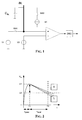
- FIG. 1 A typical circuit diagram for read (evaluation) operations of NAND memory devices is depicted in Figure 1.
- the scheme contemplates the charging to a certain read voltage V1 of the capacitance associated to a bitline BL.
- V1 the capacitance associated to a bitline BL.
- the switch SW1 opens, leaving the bitline BL charged at the read voltage V1.
- the NAND string to which the selected cell belongs is activated through a row decoding circuit, electrically represented by the switch SW2 and the relative current generator Icell of Figure 1.
- the current generator Icell starts to discharge the bitline BL at the instant T1.
- V BL t V ⁇ 1 - Icell * Teval / C BL
- Teval T ⁇ 2 - T ⁇ 1
- the result of the comparison between the voltage on the bitline BL and the discrimination voltage threshold V2 determines the value that is recognized by the discriminating circuit DEC, according to the following criteria: if VBL T ⁇ 2 > V ⁇ 2 Cell @ ⁇ 0 else Cell @ ⁇ 0 end if .
- V 2 V 1 - Icell * Teval / C BL
- FIG. 5 are depicted the currents through a cell during the charging phase (time interval 0-T1) and diving the discharge phase (in the interval from T1 to T2) for three different bitlines BL, having respectively a minimum capacitance (Cmin), a typical capacitance (Ctyp) and a maximum capacitance (Cmax) of the indicated range of variability.
- Cmin minimum capacitance
- Ctyp typical capacitance
- Cmax maximum capacitance
- Figure 6 represents the electric charge Q Cmax Q Cmin and Q Ctyp that is stored in the respective bitline.
- the turning point of a cell shifts considerably over its characteristic. Therefore, when designing the memory device it must be ensured that for any possible value of capacitance of the single array bitline there will be a working point (or turning point current) (Iturn ⁇ ICmax) that will have an adequate safety margin in order to avoid zones strongly non linear of the characteristic curve (e.g. the bottom and top darker regions in the diagram of Figure 7).
- a working point or turning point current
- the evaluation time (Teval) of the programmed or erased state of a cell of the NAND memory array is set for the individual memory device in a way that at least partially compensates the generally large spread of parasitic capacitance values of the array bitlines in the mass production fabrication process of these devices.
- the optimized establishing of working parameters of the single device may even be implemented by adjusting the difference between the read charge voltage (V1) and the read discrimination voltage (V2), or alternatively the fixing of the evaluation time (Teval) may compensate a process spread of such a voltage difference, as will be evident to the skilled reader.
- an average value of capacitance of a single bitline of the memory array assessed for a certain lot of wafers is used during the test-on-wafer phase for fixing the most appropriate evaluation time, thus taking advantage of the significantly narrower intra-lot spread of bitline parasitic capacitance values compared to the compounded spread indicated in the design rule manual of the device.
- a more preferred embodiment contemplates the integration of dedicated internal circuit structures for measuring the average parasitic capacitance of the bitlines of the memory cell array of the individual device.
- one or more dummy bitlines and associated circuit structures are formed for measuring the average time needed by the dummy bitlines to discharge from the read charge voltage V1 to the read discrimination voltage V2 with a desired current Icella.
- the evaluation time Teval is fixed equal to the so measured time interval.
- This invention provides several methods for fixing the evaluation time necessary for discriminating the state of a memory cell being read.
- a first and a second method of this invention contemplate the operation of determining the evaluation time by measuring during a test on wafer (EWS) phase the mean capacitance C BL of the bitlines and calculating in function thereof and of the read charge voltage V1, the read discrimination voltage V2 and of a certain pre-established discharge current Icell through the cell during a read operation.
- EWS test on wafer
- the evaluation time Teval may be fixed once and for all by trimming fuses of the nonvolatile memory device during the EWS phase, or it may be fixed at each power on of the memory device, or when an erase phase or a read phase is started.
- the mean capacitance C BL of the bitlines may be determined during an EWS phase of the device being fabricated by measuring the capacitance of the bitlines of the memory device ( Figure 8) or of the bitlines of all the memory devices on a same wafer ( Figure 9). Indeed, it has been noticed that the capacitance measured in this phase is determined with a range of tolerance relevantly smaller than that indicated in the Design Rule Manual ( Figure 4), thus using the so calculated mean value allows to determine in a more precise manner the evaluation time Teval.
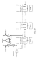
- Figure 13 depicts a memory device of this invention that integrates a dedicated circuit (drawn with a thick line) for measuring the mean capacitance C BL .
- This dedicated circuit allows to calculate the total capacitance of a plurality of bitlines, by connecting in parallel to a common line VIRPWR the plurality of bitlines, for example the even or the odd bitlines of the memory device, then the mean capacitance C BL is obtained by dividing the total capacitance by the number of bitlines connected in parallel.
- the total capacitance is measured as follows. First, all the bitlines of the memory device are grounded by connecting them to the common line VIRPWR. This is done by enabling the signals DISCHE and DISCHO ( Figure 14) when the line VIRPWR is at a ground potential, that is when the signal VIRPWRTOGND is active.
- the circuit of Figure 17 is preferred.
- the functioning is similar to that of the circuit of Figure 14, but the common line VIRPWR is charged by a current generator I EXT connected to it through a pad of the memory device.
- the value C BL does not depend on the resistance R3.
- the evaluation time Teval may be fixed without measuring the mean capacitance of the bitlines. This may be done in a memory device of Figure 19, that includes spare memory cells connected to dummy bitlines BLEDUMMY, BLODUMMY controlled by a properly designed page buffer PB DUMMY.
- Figure 20 depicts a more detailed view of the memory device of Figure 19, that shows also how a microcontroller ⁇ C conditions all the page buffers of the memory device.
- the capacitance of the dummy bitline BLEDUMMY or BLODUMMY (or the mean capacitance of all the dummy bitlines of the memory device), be substantially equal to the mean capacitance of the bitlines addressable by a user.
- the evaluation time Teval is the time required by a dummy bitline BLEDUMMY (or BLODUMMY) to discharge from the charge read voltage V1 to the discrimination read voltage V2 when a current Icell is drawn therethrough.
- the signals SELBLE and SELBLEDUM are made equal to the voltage V1, thus the dummy bitline BLEDUMMY (or BLODUMMY) and the bitlines addressable by the user are biased approximately with the voltage V1 (as a matter of fact they are biased with the voltage V1-Vth wherein Vth is the threshold voltage of the selection switch).
- the microcontroller ⁇ C enables a start flag STARTBLDISCH and the current generator Icell starts discharging the dummy line BLEDUMMY.
- the microcontroller ⁇ C fixes the time Teval as the time interval between an active edge of the start flag STARTBLDISCH and the subsequent edge of the flag ENDBLDISCH.
- This method of fixing the evaluation time Teval is particularly convenient because it may be implemented at each power on of the memory device, or at the beginning of each erase phase or even before executing each read phase. Therefore, even if the capacitance of addressable bitlines of the memory device varies, because of fluctuations of temperature or of other functioning conditions, this technique may provide the value Teval for correctly discriminating the state of the memory cells.
- Figure 21 is a detailed view of a sample embodiment of the dummy page buffer PB DUMMY of Figure 20.
- Figure 22 is a time diagram of the signals of Figure 21, that illustrates the above described technique.
Landscapes
- Read Only Memory (AREA)
- Tests Of Electronic Circuits (AREA)
Abstract

Description
- The present invention relates generally to non volatile memory devices and more particularly to NAND-type devices.
- The evaluation time of the programmed or erased state of a cell of a non volatile NAND memory array during read or verify operations is normally fixed during a test-on-wafer phase of the devices or is set by a known board microcontroller at a power on of the device by executing a self-configuration program code stored, together with pre-established configuration values.
- A typical circuit diagram for read (evaluation) operations of NAND memory devices is depicted in Figure 1.
- The scheme contemplates the charging to a certain read voltage V1 of the capacitance associated to a bitline BL. Referring to the diagram of Figure 1 and to the relative timing diagram of Figure 2, at the instant T1, the switch SW1 opens, leaving the bitline BL charged at the read voltage V1. Simultaneously, the NAND string to which the selected cell belongs is activated through a row decoding circuit, electrically represented by the switch SW2 and the relative current generator Icell of Figure 1.
- Assuming that the current flowing through the cell string is constant and depends solely from the threshold voltage of the selected cell and from the voltage of the selected wordline WL, the current generator Icell starts to discharge the bitline BL at the instant T1.
- Accordingly the voltage on the bitline BL evolves according to the following equation:

- The evaluation time interval is given by:

- At the end of the evaluation time internal Teval, that is at the instant T2, the result of the comparison between the voltage on the bitline BL and the discrimination voltage threshold V2, determines the value that is recognized by the discriminating circuit DEC, according to the following criteria:

- When programming a cell threshold voltage is incremented as far as, for a predetermined voltage (PV) applied to the relative wordline WL, the current flowing through the cell at the end of the evaluation time will have decreased to a value such that:

and therefore the cell will be recognized as having a logic "0" content, as depicted in Figure 3. - At equilibrium, the following equation holds;

- Once the voltage levels V1 and V2 and the evaluation time interval Teval are fixed, the maximum value of current flowing through the cell for which the cell is recognized as being programmed to the logic value "0" will be determined by the capacitance of the relative bitline BL, being

- Should the capacitance of all the bitlines of the memory array be equal, all the cells would have the same discharge current. Unfortunately this is not the case because the capacitance of the bitlines as normally set out in a design rule manual of these memory devices, is extremely variable, normally being indicated with ± 50% range of variability, as graphically depicted in Figure 4.
- As a consequence, the value of the current flowing through a cell, given by the relationship (6), has a large variance.
- In Figure 5 are depicted the currents through a cell during the charging phase (time interval 0-T1) and diving the discharge phase (in the interval from T1 to T2) for three different bitlines BL, having respectively a minimum capacitance (Cmin), a typical capacitance (Ctyp) and a maximum capacitance (Cmax) of the indicated range of variability.
- Figure 6 represents the electric charge QCmax QCmin and QCtyp that is stored in the respective bitline.
- Thus, the turning point of a cell shifts considerably over its characteristic. Therefore, when designing the memory device it must be ensured that for any possible value of capacitance of the single array bitline there will be a working point (or turning point current) (Iturn < ICmax) that will have an adequate safety margin in order to avoid zones strongly non linear of the characteristic curve (e.g. the bottom and top darker regions in the diagram of Figure 7).
- With the constant reduction of the sizes of integrated structures, the maximum current through the cells (Icell max) diminishes while the spread of parasitic capacitance values of the bitlines increases. This makes more and more difficult to define an operating zone of guaranteed correct functioning.
- A campaign of tests has revealed that the spread of bitline parasitic capacitance values that is commonly reported in a design rule manual of memory devices in order to enable the designer to establish with a sufficiently safe margin factor in defining the operating point or zone of operation that will ensure a faultless functioning of the device and that is replicated in the graphical representation of Figure 8, compounds in fact different spread contributions, namely an intra-die topological variability, a intra-lot of wafer spread as depicted in Figure 9, and the spread among different lots of wafers as depicted in Figure 10.
- Recognition of the relative weights of the above mentioned bitline parasitic capacitance value spread contributions to the compound spread values indicated in design rule manuals, has lead the applicants to envisage an effective way of contrasting the shrinking of the secure operating zone of the electrical characteristics of scalded down cell arrays of the memory device through an improved method of fixing an appropriate evaluation time interval (Teval) on the basis of a specific parasitic capacitance value of the bitlines of the memory cell array assessed for each individual device either once for all during a test-on-wafer phase or even repeatedly in utilizing the finished memory device.
- According to this invention, the evaluation time (Teval) of the programmed or erased state of a cell of the NAND memory array is set for the individual memory device in a way that at least partially compensates the generally large spread of parasitic capacitance values of the array bitlines in the mass production fabrication process of these devices.
- Of course, the optimized establishing of working parameters of the single device may even be implemented by adjusting the difference between the read charge voltage (V1) and the read discrimination voltage (V2), or alternatively the fixing of the evaluation time (Teval) may compensate a process spread of such a voltage difference, as will be evident to the skilled reader.
- According to a preferred embodiment of this invention, an average value of capacitance of a single bitline of the memory array assessed for a certain lot of wafers is used during the test-on-wafer phase for fixing the most appropriate evaluation time, thus taking advantage of the significantly narrower intra-lot spread of bitline parasitic capacitance values compared to the compounded spread indicated in the design rule manual of the device.
- A more preferred embodiment contemplates the integration of dedicated internal circuit structures for measuring the average parasitic capacitance of the bitlines of the memory cell array of the individual device.
- According to yet another embodiment of this invention, one or more dummy bitlines and associated circuit structures are formed for measuring the average time needed by the dummy bitlines to discharge from the read charge voltage V1 to the read discrimination voltage V2 with a desired current Icella. Given that it may be reasonably supposed that the dummy bitlines have the same capacitance of the user addressable bitlines, the evaluation time Teval is fixed equal to the so measured time interval.
- The invention is defined in the annexed claims.
- Sample embodiments of the invention will be described referring to the attached drawings, wherein:
- Figure 1 depicts schematically a bitline of a nonvolatile NAND memory device and the circuit used for discriminating the state of a cell;
- Figure 2 is a graph of the charge voltage of a bitline during a read operation;
- Figure 3 depicts four sample voltage-current characteristics of a memory cell;
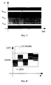
- Figure 4 depicts a sample range of tolerance of the mean value of the capacitance of a bitline as indicated in the Design Rule Manual;
- Figure 5 is a graph of the maximum, minimum and typical discharge current of a bitline during a read operation;
- Figure 6 is a graph of the maximum, minimum and typical electric charge stored in a bitline during a read operation;
- Figure 7 highlights the preferred functioning zone of the voltage-current characteristic of a bitline;
- Figure 8 depicts a typical range of tolerance of the mean value of the capacitance of the bitlines of a memory device as measured during a test on wafer (EWS) phase;
- Figure 9 depicts a typical range of tolerance of the mean value of the capacitance of the bitlines of all memory devices of a wafer as measured during a test on wafer (EWS) phase;
- Figure 10 is a basic flow chart that shows how the EWS phase is modified according to a first embodiment of this invention;
- Figure 11 depicts the page buffers and the selection switches of the bitlines of a nonvolatile NAND memory device;
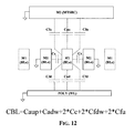
- Figure 12 illustrates the various coupling capacitances of a bitline with various parts of the memory device;
- Figure 13 depicts a first embodiment of a nonvolatile memory device of this invention that includes a circuit for establishing an evaluation time for discriminating the state of a cell being read;
- Figures 14 and 15 illustrate two functioning conditions of the device of Figure 13;
- Figure 16 depicts time graphs of the main signals of the memory device of Figures 14 and 15;
- Figure 17 depicts a second embodiment of a nonvolatile memory device of this invention that includes another circuit for establishing an evaluation time for discriminating the state of a cell being read;
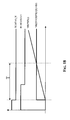
- Figure 18 depicts time graphs of the main signals of the memory device of Figure 17;
- Figure 19 schematically illustrate a third embodiment of a nonvolatile memory device of this invention that includes at least a dummy bitline and a dummy page buffer specifically designed for establishing the evaluation time of the bitlines effectively made available to a user;
- Figure 20 schematically illustrates how a microprocessor integrated in the memory device of Figure 19 measures the evaluation time of a dummy bitline and uses this information for controlling the page buffers of the memory;
- Figure 21 is a detailed view of the dummy page buffer depicted in Figures 19 and 20;
- Figure 22 depicts time graphs of the main signals of the memory device of Figures 20 and 21.
- This invention provides several methods for fixing the evaluation time necessary for discriminating the state of a memory cell being read.
- A first and a second method of this invention contemplate the operation of determining the evaluation time by measuring during a test on wafer (EWS) phase the mean capacitance CBL of the bitlines and calculating in function thereof and of the read charge voltage V1, the read discrimination voltage V2 and of a certain pre-established discharge current Icell through the cell during a read operation.
- According to an innovative aspect of the first and second method of this invention, the evaluation time Teval may be fixed once and for all by trimming fuses of the nonvolatile memory device during the EWS phase, or it may be fixed at each power on of the memory device, or when an erase phase or a read phase is started.
- The mean capacitance CBL of the bitlines may be determined during an EWS phase of the device being fabricated by measuring the capacitance of the bitlines of the memory device (Figure 8) or of the bitlines of all the memory devices on a same wafer (Figure 9). Indeed, it has been noticed that the capacitance measured in this phase is determined with a range of tolerance relevantly smaller than that indicated in the Design Rule Manual (Figure 4), thus using the so calculated mean value allows to determine in a more precise manner the evaluation time Teval.
- It is evident that carrying out such a modified EWS phase, schematically sketched in Figure 10, on a NAND memory device (Figure 11) being fabricated would significantly improve the precision of the discrimination of the state of a cell being read, and thus reduce the error probability of a read operation.
- As an alternative, it is possible to measure the mean total capacitance value CBL of a bitline, that is the sum of various contributions (Figure 12), with a dedicated circuit integrated with the memory device, and using the value CBL for fixing the evaluation time at the power on of the memory device or when an erase or read operation is started.
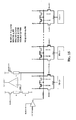
- Figure 13 depicts a memory device of this invention that integrates a dedicated circuit (drawn with a thick line) for measuring the mean capacitance CBL. This dedicated circuit allows to calculate the total capacitance of a plurality of bitlines, by connecting in parallel to a common line VIRPWR the plurality of bitlines, for example the even or the odd bitlines of the memory device, then the mean capacitance CBL is obtained by dividing the total capacitance by the number of bitlines connected in parallel.
- More in detail, the total capacitance is measured as follows. First, all the bitlines of the memory device are grounded by connecting them to the common line VIRPWR. This is done by enabling the signals DISCHE and DISCHO (Figure 14) when the line VIRPWR is at a ground potential, that is when the signal VIRPWRTOGND is active.
- Then the odd or even bitlines are kept grounded (Figure 15) by disabling the signal DISCHO or DISCHE and enabling the signals SELBLO or SELBLE, respectively. While the odd or even bitlines, respectively, are kept grounded, the signal BLMEAS_N is disabled (Figure 16), thus the common line VIRPWR is left floating (threestated) and it is charged through the resistor R3. When the voltage on the threestated common line VIRPWR reaches the reference voltage VREF generated by the voltage divider R1, R2, the flag BLMEASOUT switches.
- By measuring the time T required for charging the common line VIRPWR, it is possible to calculate the total capacitance of the even or odd (or of all the) bitlines. Indeed,

and the voltage on the common line VIRPWR increases according to the following equation:
being n the number of bitlines connected in parallel to the common line VIRPWR. Therefore, when the flag BLMEASOUT switches, a time T has elapsed such that
- By measuring this time interval T, it is possible to calculate the mean capacitance value CBL using the following equation:

- It is worth noticing that tolerances of fabrication of the resistor R3 may increase the uncertainty range of CBL. For this reason according to another embodiment of this invention, the circuit of Figure 17 is preferred. The functioning is similar to that of the circuit of Figure 14, but the common line VIRPWR is charged by a current generator IEXT connected to it through a pad of the memory device. In this case, the voltage on the line VIRPWR increases (Figure 18) according to the following equation:

thus the time T satisfies the following equation:
and the mean capacitance value CBL is
- Therefore, the value CBL does not depend on the resistance R3.
- According to another embodiment of this invention, the evaluation time Teval may be fixed without measuring the mean capacitance of the bitlines. This may be done in a memory device of Figure 19, that includes spare memory cells connected to dummy bitlines BLEDUMMY, BLODUMMY controlled by a properly designed page buffer PB DUMMY.
- Figure 20 depicts a more detailed view of the memory device of Figure 19, that shows also how a microcontroller µC conditions all the page buffers of the memory device.
- In practice, according to another method of this invention for fixing the evaluation time Teval, it is supposed that the capacitance of the dummy bitline BLEDUMMY or BLODUMMY (or the mean capacitance of all the dummy bitlines of the memory device), be substantially equal to the mean capacitance of the bitlines addressable by a user. With this assumption, the evaluation time Teval is the time required by a dummy bitline BLEDUMMY (or BLODUMMY) to discharge from the charge read voltage V1 to the discrimination read voltage V2 when a current Icell is drawn therethrough.
- More in detail, first the signals SELBLE and SELBLEDUM are made equal to the voltage V1, thus the dummy bitline BLEDUMMY (or BLODUMMY) and the bitlines addressable by the user are biased approximately with the voltage V1 (as a matter of fact they are biased with the voltage V1-Vth wherein Vth is the threshold voltage of the selection switch).
- Then the signal SELBLE is grounded and SELBLEDUM is set to the discrimination voltage V2. At the same time, the microcontroller µC enables a start flag STARTBLDISCH and the current generator Icell starts discharging the dummy line BLEDUMMY.
- When the voltage on the dummy bitline BLEDUMMY drops such to turn off the respective selection switch (that is the voltage on the bitline dummy is V2-Vth), the dummy page buffer PB DUMMY detects this event and switches the flag ENDBLDISCH. Therefore, the microcontroller µC fixes the time Teval as the time interval between an active edge of the start flag STARTBLDISCH and the subsequent edge of the flag ENDBLDISCH.
- This method of fixing the evaluation time Teval is particularly convenient because it may be implemented at each power on of the memory device, or at the beginning of each erase phase or even before executing each read phase. Therefore, even if the capacitance of addressable bitlines of the memory device varies, because of fluctuations of temperature or of other functioning conditions, this technique may provide the value Teval for correctly discriminating the state of the memory cells.
- Figure 21 is a detailed view of a sample embodiment of the dummy page buffer PB DUMMY of Figure 20.
- Figure 22 is a time diagram of the signals of Figure 21, that illustrates the above described technique.
- It is worth remarking that it is possible to connect n dummy bitlines in parallel and determining the evaluation time Teval according to the previous technique by using a discharge current generator that draws a current n*Icell.
Claims (12)
- A method of fixing an evaluation time (Teval) of the programmed or erased state of a cell of an array of rows and columns of cells of a non volatile NAND memory device, individually addressable through word lines and bitlines chargeable at certain read voltage levels, passed which from the instant the bitlines of said cell is charged at a read charge voltage (V1), a sense circuit assesses the state of the cell in order to produce at output of the memory device a certain red data, comprising the step of fixing said evaluation time (Teval) of each memory device in function of at least said read charge voltage (V1) of the bitline, of a read discriminating voltage (V2) and of a certain discharge current through the cells (Icell) once for all during a test-on-wafer phase (EWS) of the device or repeatedly during operation of the finished memory device.
- The method of claim 1, characterized by comprising the steps of establishing an average value of capacitance (CBL) of a single bitline of the memory array by measuring the capacitance of a predefined plurality of bitlines of the memory array;
fixing said evaluation time (Teval) of each memory device so in function of said average capacitance value (CBL) of a bitline. - The method according to claim 1, wherein said evaluation time (Teval) is fixed at a phase of operation of the memory device chosen from the power-on phase and at start of an erase or read operation.
- The method according to claim 2, including the steps of:measuring the total capacitance of even or odd bitlines of the memory array;establishing said average value of bitline capacitance (CBL) by dividing the measured capacitance by the number of either even or odd bitlines charged to said read charge voltage (V1) in parallel.
- The method of claim 4, comprising the steps of:biasing either all even or all odd bitlines of the memory array by connecting them in parallel to a common ground line;charging in parallel said bitlines by connecting said common line to a power supply rail of the memory device through an auxiliary resistance (R3);comparing the voltage on said common line with a reference voltage VREF;measuring the charging time (T) of said bitlines for reaching on said common line a voltage equal to said reference voltage (VREF);calculating the total capacitance of said bitlines in function of said time of charging (T) of said auxiliary resistance (R3) and of said reference voltage (VREF).
- The method of claim 4, comprising the steps of
biasing either all even or all odd bitlines of the memory array by connecting them in parallel to a common ground line;
charging in parallel said bitlines by connecting said common line to a constant current generator of a certain current (IEXT);
comparing the voltage on said common line with a reference voltage VREF;
measuring the charging time (T) of said bitlines for reaching on said common line a voltage equal to said reference voltage (VREF);
calculating the total capacitance of said bitlines in function of said time of charging (T) of said auxiliary resistance (R3) and of said reference voltage (VREF). - The method of claim 3, wherein said memory device comprises additional dummy bitlines memory cells, the method comprising the steps of biasing at least one of said dummy bitlines at said red charging voltage (V1);
discharging said dummy bitlines at said certain pre-established discharge current (Icell);
fixing said evaluation time (Teval) by measuring the time needed for discharging said dummy bitline from said read charging voltage (V1) to said read discrimination voltage level (V2). - A non volatile NAND type memory device including a circuit for fixing an evaluation time (Teval) of the programmed or erased state of a cell of an array of rows and columns of cells, individually addressable through word lines and bitlines chargeable at respective read charging voltages, a method of fixing an evaluation time (Teval) of the programmed or erased state of a cell of an arrays of rows and columns of cells of a non volatile NAND memory device, individually addressable through word lines and bitlines chargeable at certain read voltage levels, passed which from the instant the bitlines of said cell is charged at a read charge voltage (V1), a sense circuit assesses the state of the cell in order to produce at output of the memory device a certain red data, comprising the step of:said circuit for fixing the evaluation time (Teval) comprising:a voltage divider (R1, R2) referred to ground and connected to a power supply line of the memory device through a switch controlled by a control signal (BLMEANS_N), generating a reference voltage (VREF);a comparator for comparing the voltage on a common line of said bitlines of the memory array with said reference voltage (VREF), generating a flag (BLMEASOUT) active when said reference voltage (VREF) is surpassed;circuit means for charging said common line of said bitlines.
- The device of claim 8, wherein said circuit means comprise an auxiliary resistance (R3) connected to said power supply line through a second switch controlled by said control signal (BLMEAS_N).
- The device of claim 8, wherein said circuit means comprise a current generator (IEXT) connected to said power supply voltage line through a pad of the memory device.
- A non volatile NAND type memory device including a circuit for fixing an evaluation time (Teval) of the programmed or erased state of a cell of an array of rows and columns of cells, individually addressable through word lines and bitlines chargeable at respective read charging voltages, a method of fixing an evaluation time (Teval) of the programmed or erased state of a cell of an arrays of rows and columns of cells of a non volatile NAND memory device, individually addressable through word lines and bitlines chargeable at certain read voltage levels, passed which from the instant the bitlines of said cell is charged at a read charge voltage (V1), a sense circuit assesses the state of the cell in order to produce at output of the memory device a certain red data, comprising the step of:at least a dummy bitline;means for loading said dummy bitline at said read charging voltage (V1);a constant current generator (Ibias) for discharging said dummy bitline when enabled by a control signal (STARTBLDISCH);a flag generating circuit (ENDBLDISCH) active when said dummy bitline reaches a pre-established read discrimination voltage level (V2);a microprocessor receiving said flag (ENDBLDISCH), for generating said control signal (STARTBLDISCH) and fixing the evaluation time (Teval) according to the method of claim 7.
- A method of testing-on-wafer (EWS) a non volatile NAND type memory device having a circuit for fixing an evaluation time (Teval) of the programmed or erased state of a cell of an array of rows and columns of cells, individually addressable through word lines and bitlines chargeable at respective read charging voltages, a method of fixing an evaluation time (Teval) of the programmed or erased state of a cell of an arrays of rows and columns of cells of a non volatile NAND memory device, individually addressable through word lines and bitlines chargeable at certain read voltage levels, passed which from the instant the bitlines of said cell is charged at a read charge voltage (V1), a sense circuit assesses the state of the cell in order to produce at output of the memory device a certain red data, comprising the following steps:establishing an average value of capacitance (CBL) of a single bitline of the memory array by measuring the capacitance of a pre-defined plurality of bitlines of said array;fixing said evaluation time (Teval) of each memory device in function of at least said read charging voltage (V1) of the bitlines, of a read discrimination voltage level (V2), of a certain discharge current through said cell (Icell) and of said average capacitance value (CBL) through the setting of trimming fuses of the memory device.
Priority Applications (4)
| Application Number | Priority Date | Filing Date | Title |
|---|---|---|---|
| DE602006013977T DE602006013977D1 (en) | 2006-09-13 | 2006-09-13 | A method of setting the read evaluation time in a non-volatile NAND memory device |
| EP06425631A EP1901309B1 (en) | 2006-09-13 | 2006-09-13 | Method of fixing read evaluation time in a non volatile nand type memory device |
| US11/854,713 US20080062767A1 (en) | 2006-09-13 | 2007-09-13 | Method of fixing a read evaluation time or the difference between a read charge voltage and a read discriminating voltage in a non-volatile nand type memory device |
| CNA2007101821636A CN101159167A (en) | 2006-09-13 | 2007-09-13 | Method of fixing read evaluation time in a non volatile nand type memory device |
Applications Claiming Priority (1)
| Application Number | Priority Date | Filing Date | Title |
|---|---|---|---|
| EP06425631A EP1901309B1 (en) | 2006-09-13 | 2006-09-13 | Method of fixing read evaluation time in a non volatile nand type memory device |
Publications (2)
| Publication Number | Publication Date |
|---|---|
| EP1901309A1 true EP1901309A1 (en) | 2008-03-19 |
| EP1901309B1 EP1901309B1 (en) | 2010-04-28 |
Family
ID=37882195
Family Applications (1)
| Application Number | Title | Priority Date | Filing Date |
|---|---|---|---|
| EP06425631A Active EP1901309B1 (en) | 2006-09-13 | 2006-09-13 | Method of fixing read evaluation time in a non volatile nand type memory device |
Country Status (4)
| Country | Link |
|---|---|
| US (1) | US20080062767A1 (en) |
| EP (1) | EP1901309B1 (en) |
| CN (1) | CN101159167A (en) |
| DE (1) | DE602006013977D1 (en) |
Families Citing this family (4)
| Publication number | Priority date | Publication date | Assignee | Title |
|---|---|---|---|---|
| KR100865820B1 (en) * | 2007-06-28 | 2008-10-28 | 주식회사 하이닉스반도체 | Memory device and read method |
| KR101449932B1 (en) * | 2013-02-18 | 2014-10-22 | (주)피델릭스 | Flash memory device reducing layout area |
| KR102820350B1 (en) * | 2017-02-06 | 2025-06-16 | 에스케이하이닉스 주식회사 | Data storage device and operating method thereof |
| US11177280B1 (en) | 2020-05-18 | 2021-11-16 | Sandisk Technologies Llc | Three-dimensional memory device including wrap around word lines and methods of forming the same |
Citations (2)
| Publication number | Priority date | Publication date | Assignee | Title |
|---|---|---|---|---|
| US20040027855A1 (en) * | 2002-08-12 | 2004-02-12 | Matrix Semiconductor, Inc. | Dynamic sub-array group selection scheme |
| EP1610335A2 (en) * | 2002-09-24 | 2005-12-28 | SanDisk Corporation | Non-volatile memory and its sensing method |
Family Cites Families (3)
| Publication number | Priority date | Publication date | Assignee | Title |
|---|---|---|---|---|
| US6222762B1 (en) * | 1992-01-14 | 2001-04-24 | Sandisk Corporation | Multi-state memory |
| US6550028B1 (en) * | 1999-10-19 | 2003-04-15 | Advanced Micro Devices, Inc. | Array VT mode implementation for a simultaneous operation flash memory device |
| US7023733B2 (en) * | 2004-05-05 | 2006-04-04 | Sandisk Corporation | Boosting to control programming of non-volatile memory |
-
2006
- 2006-09-13 EP EP06425631A patent/EP1901309B1/en active Active
- 2006-09-13 DE DE602006013977T patent/DE602006013977D1/en active Active
-
2007
- 2007-09-13 US US11/854,713 patent/US20080062767A1/en not_active Abandoned
- 2007-09-13 CN CNA2007101821636A patent/CN101159167A/en active Pending
Patent Citations (2)
| Publication number | Priority date | Publication date | Assignee | Title |
|---|---|---|---|---|
| US20040027855A1 (en) * | 2002-08-12 | 2004-02-12 | Matrix Semiconductor, Inc. | Dynamic sub-array group selection scheme |
| EP1610335A2 (en) * | 2002-09-24 | 2005-12-28 | SanDisk Corporation | Non-volatile memory and its sensing method |
Also Published As
| Publication number | Publication date |
|---|---|
| US20080062767A1 (en) | 2008-03-13 |
| CN101159167A (en) | 2008-04-09 |
| DE602006013977D1 (en) | 2010-06-10 |
| EP1901309B1 (en) | 2010-04-28 |
Similar Documents
| Publication | Publication Date | Title |
|---|---|---|
| JP3866627B2 (en) | Nonvolatile semiconductor memory | |
| US10629272B1 (en) | Two-stage ramp up of word line voltages in memory device to suppress read disturb | |
| EP3669367B1 (en) | Reducing injection type of read disturb in a cold read of a memory device | |
| US6819596B2 (en) | Semiconductor memory device with test mode | |
| KR100858745B1 (en) | Efficient verification for coarse/fine programming of non-volatile memory | |
| US6396742B1 (en) | Testing of multilevel semiconductor memory | |
| KR102568555B1 (en) | Temperature and Cycling Dependent Refresh Behavior for Memory Cells | |
| US11657883B2 (en) | Isolating problematic memory planes to avoid neighbor plan disturb | |
| US7457165B2 (en) | Non-volatile memory device and method of programming same | |
| KR20130069526A (en) | Non-volatile memory device | |
| CN114730601A (en) | Refresh operation based on memory cells sensitive to read errors | |
| WO2019221791A1 (en) | Memory device with vpass step to reduce hot carrier injection type of program disturb | |
| WO2021021251A1 (en) | Maintaining channel pre-charge in program operation | |
| US20060164898A1 (en) | Exploiting a statistical distribution of the values of an electrical characteristic in a population of auxiliary memory cells for obtaining reference cells | |
| KR20020091581A (en) | Flash memory device capable of checking memory cells with progressive fail characteristic | |
| US20080062767A1 (en) | Method of fixing a read evaluation time or the difference between a read charge voltage and a read discriminating voltage in a non-volatile nand type memory device | |
| WO2002089144A1 (en) | Accurate verify apparatus and method for nor flash memory cells in the presence of high column leakage | |
| US7315482B2 (en) | Memory device with a plurality of reference cells on a bit line | |
| CN113168868A (en) | Memory device with charge isolation to reduce injection-type program disturb | |
| EP0698890B1 (en) | Testing an integrated circuit device | |
| WO2021167638A1 (en) | Reprogramming memory cells to tighten threshold voltage distributions and improve data retention | |
| TW201637020A (en) | Average voltage band detection and use for tuning of voltages in asics |
Legal Events
| Date | Code | Title | Description |
|---|---|---|---|
| PUAI | Public reference made under article 153(3) epc to a published international application that has entered the european phase |
Free format text: ORIGINAL CODE: 0009012 |
|
| AK | Designated contracting states |
Kind code of ref document: A1 Designated state(s): AT BE BG CH CY CZ DE DK EE ES FI FR GB GR HU IE IS IT LI LT LU LV MC NL PL PT RO SE SI SK TR |
|
| AX | Request for extension of the european patent |
Extension state: AL BA HR MK YU |
|
| 17P | Request for examination filed |
Effective date: 20080917 |
|
| AKX | Designation fees paid |
Designated state(s): DE |
|
| 17Q | First examination report despatched |
Effective date: 20081112 |
|
| GRAP | Despatch of communication of intention to grant a patent |
Free format text: ORIGINAL CODE: EPIDOSNIGR1 |
|
| GRAS | Grant fee paid |
Free format text: ORIGINAL CODE: EPIDOSNIGR3 |
|
| GRAA | (expected) grant |
Free format text: ORIGINAL CODE: 0009210 |
|
| RAP1 | Party data changed (applicant data changed or rights of an application transferred) |
Owner name: STMICROELECTRONICS SRL Owner name: HYNIX SEMICONDUCTOR INC. |
|
| AK | Designated contracting states |
Kind code of ref document: B1 Designated state(s): DE |
|
| REF | Corresponds to: |
Ref document number: 602006013977 Country of ref document: DE Date of ref document: 20100610 Kind code of ref document: P |
|
| PLBE | No opposition filed within time limit |
Free format text: ORIGINAL CODE: 0009261 |
|
| STAA | Information on the status of an ep patent application or granted ep patent |
Free format text: STATUS: NO OPPOSITION FILED WITHIN TIME LIMIT |
|
| 26N | No opposition filed |
Effective date: 20110131 |
|
| PGFP | Annual fee paid to national office [announced via postgrant information from national office to epo] |
Ref country code: DE Payment date: 20250926 Year of fee payment: 20 |