EP1895694A2 - Receiving Apparatus - Google Patents
Receiving Apparatus Download PDFInfo
- Publication number
- EP1895694A2 EP1895694A2 EP07114974A EP07114974A EP1895694A2 EP 1895694 A2 EP1895694 A2 EP 1895694A2 EP 07114974 A EP07114974 A EP 07114974A EP 07114974 A EP07114974 A EP 07114974A EP 1895694 A2 EP1895694 A2 EP 1895694A2
- Authority
- EP
- European Patent Office
- Prior art keywords
- signals
- circuit
- frequency
- band
- frequency band
- Prior art date
- Legal status (The legal status is an assumption and is not a legal conclusion. Google has not performed a legal analysis and makes no representation as to the accuracy of the status listed.)
- Withdrawn
Links
- 230000002265 prevention Effects 0.000 claims description 2
- 101100536354 Drosophila melanogaster tant gene Proteins 0.000 description 10
- 239000003990 capacitor Substances 0.000 description 8
- 238000010586 diagram Methods 0.000 description 4
- 239000000284 extract Substances 0.000 description 3
- 238000000034 method Methods 0.000 description 2
- 238000012986 modification Methods 0.000 description 1
- 230000004048 modification Effects 0.000 description 1
- 239000004065 semiconductor Substances 0.000 description 1
Images



Classifications
-
- H—ELECTRICITY
- H04—ELECTRIC COMMUNICATION TECHNIQUE
- H04H—BROADCAST COMMUNICATION
- H04H40/00—Arrangements specially adapted for receiving broadcast information
- H04H40/18—Arrangements characterised by circuits or components specially adapted for receiving
- H04H40/27—Arrangements characterised by circuits or components specially adapted for receiving specially adapted for broadcast systems covered by groups H04H20/53 - H04H20/95
-
- H—ELECTRICITY
- H04—ELECTRIC COMMUNICATION TECHNIQUE
- H04H—BROADCAST COMMUNICATION
- H04H20/00—Arrangements for broadcast or for distribution combined with broadcast
- H04H20/65—Arrangements characterised by transmission systems for broadcast
- H04H20/71—Wireless systems
- H04H20/72—Wireless systems of terrestrial networks
Definitions
- the present invention relates generally to receiving apparatuses, and more particularly to a receiving apparatus with a receiving circuit for receiving signals of a first frequency band and signals of a second frequency band.
- DAB digital audio broadcasting
- FM frequency modulation
- FIG. 4 is a block diagram of a conventional digital audio broadcast receiving apparatus.
- a digital audio broadcast receiving apparatus 10 includes capacitors C11, C12, a high-frequency circuit 11, and a demodulator circuit 12.
- High-frequency signals are supplied from an antenna to an antenna terminal Tant.
- the high-frequency signals supplied to the antenna terminal Tant are supplied to a Band 3/FM input terminal Tin1 of the high-frequency circuit 11 via the capacitor C11 and to an L-band input terminal Tin2 of the high-frequency circuit 11 via the capacitor C12.
- the high-frequency circuit 11 primarily includes one semiconductor chip.
- the high-frequency circuit 11 extracts from the demodulator circuit 12 high-frequency signals corresponding to channel select signals, and supplies the extracted high-frequency signals to the demodulator circuit 12.
- the demodulator circuit 12 demodulates the high-frequency signals received from the high-frequency circuit 11 and supplies them to an external circuit.
- the frequency band (174 MHz through 242 MHz) of Band 3 includes a higher harmonic wave (216 MHz) that is two times as high as a receivable frequency band of FM broadcast (108 MHz). Accordingly, in an area where the strength for Band 3 is generally low and the strength for FM broadcast of 108 MHz is generally high, a higher harmonic wave (216 MHz) that is two times as high as the receivable frequency band of FM broadcast is superimposed onto Band 3 as noise. This noise obstructs the reception of Band 3.
- each band-pass filter extracts signals of the desired frequency band (see Patent Documents 1, 2).
- Patent Document 1 Japanese Laid-Open Utility Model Application No. H5-48440
- Patent Document 2 Published Japanese Translation of PCT International Publication (for Patent Application) No. 2004-502375
- the present invention provides a receiving apparatus in which one or more of the above-described disadvantages are eliminated.
- a preferred embodiment of the present invention provides a receiving apparatus in which higher harmonic waves can be reduced.
- An embodiment of the present invention provides a receiving apparatus including a receiving circuit configured to receive signals of a first frequency band and signals of a second frequency band; a filter (111) configured to allow the signals of the first frequency band to pass through the filter and be supplied to the receiving circuit, and to attenuate the signals of the second frequency band; and a switch unit (112) provided in parallel with the filter (111) and configured to allow the signals to pass through or prevent the signals from passing through based on a control signal.
- a receiving apparatus includes a receiving circuit configured to receive signals of a first frequency band and signals of a second frequency band; a filter (111) configured to allow the signals of the first frequency band to pass through the filter and be supplied to the receiving circuit, and to attenuate the signals of the second frequency band; and a switch unit (112) provided in parallel with the filter (111) and configured to allow the signals to pass through or prevent the signals from passing through based on a control signal. Therefore, when the switch unit (112) switches on based on the control signal, signals of both the first and second frequency bands are supplied to the receiving circuit. When the switch unit (112) switches off based on the control signal, signals of only the first frequency band that have passed through the filter (111) are supplied to the receiving circuit. Hence, it is possible to reduce the intrusion of higher harmonic waves.
- FIG. 1 is a block diagram of a receiving apparatus according to an embodiment of the present invention.
- a receiving apparatus 100 is for receiving DAB, and includes capacitors C11, C12, a filter circuit (band-pass filter) 111, a switch circuit 112, a high-frequency circuit 11, and a demodulator circuit 113.
- an antenna terminal Tant receives signals from an antenna.
- the antenna terminal Tant is connected to the band-pass filter 111 via the capacitor C11 and also to an L-band input terminal Tin2 of the high-frequency circuit 11 via the capacitor C12.
- the capacitors C11, C12 remove direct-current components from signals received from the antenna terminal Tant.
- the frequency band of the band-pass filter 111 is specified so that signals of frequency bands of DAB and Band 3 can pass through the band-pass filter 111. Signals that have passed through the band-pass filter 111 are supplied to a Band 3/FM signal input terminal Tin1 of the high-frequency circuit 11.
- the switch circuit 112 is connected in parallel with the high-frequency circuit 11.
- the switch circuit 112 includes a PIN (positive-intrinsic-negative) diode D11, resistances R11, R12, and a coil L11.
- PIN positive-intrinsic-negative
- the PIN diode D11 is connected in parallel with the band-pass filter 111.
- the anode of the PIN diode D11 is connected to the connection point of the capacitor C11 and the band-pass filter 111 and the cathode of the PIN diode D11 is connected to the Band 3/FM signal input terminal Tin1 of the high-frequency circuit 11.
- the PIN diode D11 is caused to switch its status when a bias voltage is applied between the anode and the cathode of the PIN diode D11 by the resistances R11, R12 and the coil L11.
- the resistance R11 has one end connected to the anode of the PIN diode D11 and the other end connected to a control terminal Tcnt2.
- the resistance R12 has one end connected to the cathode of the PIN diode D11 and the other end connected to one end of the coil L11. The other end of the coil L11 is grounded.
- a direct-current voltage is applied from the demodulator circuit 113 to the control terminal Tcnt2 of the switch circuit 112.
- a direct-current voltage is applied to the control terminal Tcnt2, the PIN diode D11 switches on.
- the resistances R11, R12 control the forward current of the PIN diode D11 to prevent unnecessary currents from flowing to the PIN diode D11.
- the coil L11 prevents signal components from flowing from the antenna terminal Tant to ground.
- the control terminal Tcnt2 of the switch circuit 112 is connected to the control terminal Tcnt3 of the demodulator circuit 113.
- Channel select information is supplied from an external circuit to a control terminal Tcnt1 of the demodulator circuit 113.
- the demodulator circuit 113 controls the high-frequency circuit 11 so that signals of frequencies corresponding to the channel select information are supplied to the demodulator circuit 113.
- the demodulator circuit 113 controls the high-frequency circuit 11 according to the channel select information received from the external circuit, and extracts, from the high-frequency circuit 11, high-frequency signals corresponding to channel select information.
- the demodulator circuit 113 demodulates the high-frequency signals supplied from the high-frequency circuit 11, and supplies them to the external circuit.
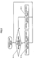
- FIG. 2 is a flowchart of a process performed by the demodulator circuit 113.
- step S1-1 when the demodulator circuit 113 receives, from an external circuit, an instruction to receive signals from an FM broadcasting station; in step S1-2 the demodulator circuit 113 turns control signals into high-level signals, which control signals are to be supplied from the control terminal Tcnt3 to the control terminal Tcnt2 of the switch circuit 112.
- the control signals supplied to the control terminal Tcnt2 become high-level, the PIN diode D11 of the switch circuit 112 is turned on.
- the PIN diode D11 When the PIN diode D11 is turned on, high-frequency signals are supplied from the antenna terminal Tant via the PIN diode D11 to the Band 3/FM signal input terminal Tin1 of the high-frequency circuit 11.
- FM signals can be supplied to the high-frequency circuit 11 without reducing the FM signals with the filter circuit 111.
- the high-frequency circuit 11 selects high-frequency signals of the frequency corresponding to the channel select information from the demodulator circuit 113, and supplies them to the demodulator circuit 113.
- the demodulator circuit 113 demodulates the high-frequency signals received from the high-frequency circuit 11 to obtain FM signals corresponding to the channel select information.
- step S1-1 when the demodulator circuit 113 receives, from an external circuit, an instruction to receive digital audio broadcasting of Band 3, in step S1-3, the demodulator circuit 113 turns control signals into low-level signals, which control signals are to be supplied from the control terminal Tcnt3 to the control terminal Tcnt2 of the switch circuit 112.
- the control signals supplied to the control terminal Tcnt2 become low-level, the PIN diode D11 of the switch circuit 112 is turned off.
- the PIN diode D11 is turned off, high-frequency signals are supplied from the antenna terminal Tant to the filter circuit 111.
- signals of the frequency band of Band 3 are selectively allowed to pass through the band-pass filter 111, and are supplied to the demodulator circuit 113.
- signals of the frequency band of Band 3 are supplied via the Band 3/FM signal input terminal Tin1 to the demodulator circuit 113. That is, higher harmonic wave components of FM signals are removed from the high-frequency signals before the signals are supplied.
- FIG. 3 is a chart for describing an operation according to an embodiment of the present invention.
- the frequency band of Band 3 is 174 MHz through 242 MHz.
- the frequency band of FM broadcasting is 108 MHz.
- a higher harmonic wave that is two times 108 MHz is 216 MHz, as indicated by a dashed line shown in FIG. 3.
- the frequency band of Band 3 is within 174 MHz through 242 MHz, and therefore, if the frequency band 108 MHz of FM broadcasting is included, reception of Band 3 is obstructed by higher harmonic noise of FM broadcasting.
- the switch circuit 112 when receiving Band 3, the switch circuit 112 is turned off so that signals from the antenna terminal Tant are supplied to the Band 3/FM signal input terminal Tin1 of the high-frequency circuit 11 through the band-pass filter 111.
- the higher harmonic wave that is two times the FM broadcast wave 108 MHz is not superimposed to the Band 3 signals as noise. Consequently, Band 3 signals can be demodulated without receiving the impact of noise.
- a receiving apparatus includes a receiving circuit configured to receive signals of a first frequency band and signals of a second frequency band; a filter (111) configured to allow the signals of the first frequency band to pass through the filter and be supplied to the receiving circuit, and to attenuate the signals of the second frequency band; and a switch unit provided in parallel with the filter and configured to switch its status based on a control signal.
- the switch unit (112) includes a diode (D11) whose anode is connected to an input end of the filter (111) and whose cathode is connected to an output end of the filter (111); and a bias circuit (R11, R12, L11) configured to apply a bias voltage to the diode (D11) based on the control signal.
- D11 diode
- R12, L11 bias circuit
- the diode (D11) includes a positive-intrinsic-negative diode.
- the bias circuit (R11, R12, L11) includes a first resistance (R11) including one end configured to receive the control signal and another end connected to the anode of the diode (D11); a second resistance (R12) comprising one end connected to the cathode of the diode (D11); and an alternating-current prevention coil (L11) comprising one end connected to another end of the second resistance (R12), and another end grounded.
- the first frequency band is used for digital audio broadcasting; and the second frequency band is used for frequency modulation broadcasting.
Landscapes
- Engineering & Computer Science (AREA)
- Signal Processing (AREA)
- Noise Elimination (AREA)
- Circuits Of Receivers In General (AREA)
- Input Circuits Of Receivers And Coupling Of Receivers And Audio Equipment (AREA)
Abstract
A disclosed receiving apparatus includes a receiving circuit configured to receive signals of a first frequency band and signals of a second frequency band; a filter (111) configured to allow the signals of the first frequency band to pass through the filter and be supplied to the receiving circuit, and to attenuate the signals of the second frequency band; and a switch unit (112) provided in parallel with the filter (111) and configured to switch its status based on a control signal.
Description
- The present invention relates generally to receiving apparatuses, and more particularly to a receiving apparatus with a receiving circuit for receiving signals of a first frequency band and signals of a second frequency band.
- In recent years and continuing, digital audio broadcasting (DAB) has been proposed and put into practice as radio broadcasting, due to requirements for higher sound quality. When DAB is practically used, it competes with existing broadcast waves such as those of FM (frequency modulation) broadcasting. For this reason, a high-frequency IC installed in a digital audio broadcast receiving apparatus is configured to receive not only DAB but also FM broadcasting. In such a high-frequency IC, in order to reduce the number of chip terminals, a signal terminal is shared by Band 3 and FM broadcasting, as they have similar receiving frequency bands.
- FIG. 4 is a block diagram of a conventional digital audio broadcast receiving apparatus.
- A digital audio
broadcast receiving apparatus 10 includes capacitors C11, C12, a high-frequency circuit 11, and ademodulator circuit 12. - High-frequency signals are supplied from an antenna to an antenna terminal Tant. The high-frequency signals supplied to the antenna terminal Tant are supplied to a Band 3/FM input terminal Tin1 of the high-
frequency circuit 11 via the capacitor C11 and to an L-band input terminal Tin2 of the high-frequency circuit 11 via the capacitor C12. - The high-
frequency circuit 11 primarily includes one semiconductor chip. The high-frequency circuit 11 extracts from thedemodulator circuit 12 high-frequency signals corresponding to channel select signals, and supplies the extracted high-frequency signals to thedemodulator circuit 12. Thedemodulator circuit 12 demodulates the high-frequency signals received from the high-frequency circuit 11 and supplies them to an external circuit. - However, the frequency band (174 MHz through 242 MHz) of Band 3 includes a higher harmonic wave (216 MHz) that is two times as high as a receivable frequency band of FM broadcast (108 MHz).
Accordingly, in an area where the strength for Band 3 is generally low and the strength for FM broadcast of 108 MHz is generally high, a higher harmonic wave (216 MHz) that is two times as high as the receivable frequency band of FM broadcast is superimposed onto Band 3 as noise. This noise obstructs the reception of Band 3. - Generally, in order to eliminate the impact of noise, a plurality of band-pass filters are provided. Each band-pass filter extracts signals of the desired frequency band (see
Patent Documents 1, 2). - Patent Document 1:
Japanese Laid-Open Utility Model Application No. H5-48440 - Patent Document 2: Published Japanese Translation of PCT International Publication (for Patent Application)
No. 2004-502375 - However, if only the frequency band of Band 3 is allowed to pass through a band-pass filter, FM broadcast cannot be received. Furthermore, if a filter is provided for each of the frequency bands to be received, the circuit configuration becomes complex and the cost increases.
- The present invention provides a receiving apparatus in which one or more of the above-described disadvantages are eliminated.
- A preferred embodiment of the present invention provides a receiving apparatus in which higher harmonic waves can be reduced.
- An embodiment of the present invention provides a receiving apparatus including a receiving circuit configured to receive signals of a first frequency band and signals of a second frequency band; a filter (111) configured to allow the signals of the first frequency band to pass through the filter and be supplied to the receiving circuit, and to attenuate the signals of the second frequency band; and a switch unit (112) provided in parallel with the filter (111) and configured to allow the signals to pass through or prevent the signals from passing through based on a control signal.
- According to one embodiment of the present invention, a receiving apparatus includes a receiving circuit configured to receive signals of a first frequency band and signals of a second frequency band; a filter (111) configured to allow the signals of the first frequency band to pass through the filter and be supplied to the receiving circuit, and to attenuate the signals of the second frequency band; and a switch unit (112) provided in parallel with the filter (111) and configured to allow the signals to pass through or prevent the signals from passing through based on a control signal. Therefore, when the switch unit (112) switches on based on the control signal, signals of both the first and second frequency bands are supplied to the receiving circuit. When the switch unit (112) switches off based on the control signal, signals of only the first frequency band that have passed through the filter (111) are supplied to the receiving circuit. Hence, it is possible to reduce the intrusion of higher harmonic waves.
- Other objects, features and advantages of the present invention will become more apparent from the following detailed description when read in conjunction with the accompanying drawings, in which:
- FIG. 1 is a block diagram of a receiving apparatus according to an embodiment of the present invention;
- FIG. 2 is a flowchart of a process performed by a demodulator circuit of the receiving apparatus shown in FIG. 1;
- FIG. 3 is a chart for describing an operation according to an embodiment of the present invention; and
- FIG. 4 is a block diagram of a conventional digital audio broadcast receiving apparatus.
- A description is given, with reference to the accompanying drawings, of an embodiment of the present invention.
- FIG. 1 is a block diagram of a receiving apparatus according to an embodiment of the present invention.
- A receiving
apparatus 100 according to an embodiment of the present invention is for receiving DAB, and includes capacitors C11, C12, a filter circuit (band-pass filter) 111, aswitch circuit 112, a high-frequency circuit 11, and ademodulator circuit 113. - In the
receiving apparatus 100, an antenna terminal Tant receives signals from an antenna. The antenna terminal Tant is connected to the band-pass filter 111 via the capacitor C11 and also to an L-band input terminal Tin2 of the high-frequency circuit 11 via the capacitor C12. The capacitors C11, C12 remove direct-current components from signals received from the antenna terminal Tant. - The frequency band of the band-
pass filter 111 is specified so that signals of frequency bands of DAB and Band 3 can pass through the band-pass filter 111. Signals that have passed through the band-pass filter 111 are supplied to a Band 3/FM signal input terminal Tin1 of the high-frequency circuit 11. Theswitch circuit 112 is connected in parallel with the high-frequency circuit 11. - The
switch circuit 112 includes a PIN (positive-intrinsic-negative) diode D11, resistances R11, R12, and a coil L11. - The PIN diode D11 is connected in parallel with the band-
pass filter 111. The anode of the PIN diode D11 is connected to the connection point of the capacitor C11 and the band-pass filter 111 and the cathode of the PIN diode D11 is connected to the Band 3/FM signal input terminal Tin1 of the high-frequency circuit 11. - The PIN diode D11 is caused to switch its status when a bias voltage is applied between the anode and the cathode of the PIN diode D11 by the resistances R11, R12 and the coil L11.
- The resistance R11 has one end connected to the anode of the PIN diode D11 and the other end connected to a control terminal Tcnt2. The resistance R12 has one end connected to the cathode of the PIN diode D11 and the other end connected to one end of the coil L11. The other end of the coil L11 is grounded.
- A direct-current voltage is applied from the
demodulator circuit 113 to the control terminal Tcnt2 of theswitch circuit 112. When a direct-current voltage is applied to the control terminal Tcnt2, the PIN diode D11 switches on. - The resistances R11, R12 control the forward current of the PIN diode D11 to prevent unnecessary currents from flowing to the PIN diode D11. The coil L11 prevents signal components from flowing from the antenna terminal Tant to ground.
- The control terminal Tcnt2 of the
switch circuit 112 is connected to the control terminal Tcnt3 of thedemodulator circuit 113. Channel select information is supplied from an external circuit to a control terminal Tcnt1 of thedemodulator circuit 113. Based on the channel select information supplied to the control terminal Tcnt1, thedemodulator circuit 113 controls the high-frequency circuit 11 so that signals of frequencies corresponding to the channel select information are supplied to thedemodulator circuit 113. - The
demodulator circuit 113 controls the high-frequency circuit 11 according to the channel select information received from the external circuit, and extracts, from the high-frequency circuit 11, high-frequency signals corresponding to channel select information. Thedemodulator circuit 113 demodulates the high-frequency signals supplied from the high-frequency circuit 11, and supplies them to the external circuit. - FIG. 2 is a flowchart of a process performed by the
demodulator circuit 113. - In step S1-1, when the
demodulator circuit 113 receives, from an external circuit, an instruction to receive signals from an FM broadcasting station; in step S1-2 thedemodulator circuit 113 turns control signals into high-level signals, which control signals are to be supplied from the control terminal Tcnt3 to the control terminal Tcnt2 of theswitch circuit 112. When the control signals supplied to the control terminal Tcnt2 become high-level, the PIN diode D11 of theswitch circuit 112 is turned on. When the PIN diode D11 is turned on, high-frequency signals are supplied from the antenna terminal Tant via the PIN diode D11 to the Band 3/FM signal input terminal Tin1 of the high-frequency circuit 11. Accordingly, FM signals can be supplied to the high-frequency circuit 11 without reducing the FM signals with thefilter circuit 111. From among high-frequency signals supplied to the Band 3/FM signal input terminal Tin1 through the PIN diode D11, the high-frequency circuit 11 selects high-frequency signals of the frequency corresponding to the channel select information from thedemodulator circuit 113, and supplies them to thedemodulator circuit 113. Thedemodulator circuit 113 demodulates the high-frequency signals received from the high-frequency circuit 11 to obtain FM signals corresponding to the channel select information. - In step S1-1, when the
demodulator circuit 113 receives, from an external circuit, an instruction to receive digital audio broadcasting of Band 3, in step S1-3, thedemodulator circuit 113 turns control signals into low-level signals, which control signals are to be supplied from the control terminal Tcnt3 to the control terminal Tcnt2 of theswitch circuit 112. When the control signals supplied to the control terminal Tcnt2 become low-level, the PIN diode D11 of theswitch circuit 112 is turned off. When the PIN diode D11 is turned off, high-frequency signals are supplied from the antenna terminal Tant to thefilter circuit 111. Among the high-frequency signals from the antenna terminal Tant, signals of the frequency band of Band 3 are selectively allowed to pass through the band-pass filter 111, and are supplied to thedemodulator circuit 113. Hence, only signals of the frequency band of Band 3 are supplied via the Band 3/FM signal input terminal Tin1 to thedemodulator circuit 113. That is, higher harmonic wave components of FM signals are removed from the high-frequency signals before the signals are supplied. - Accordingly, higher harmonic wave noise is prevented from being superimposed on Band 3 signals, and therefore, Band 3 signals can be reliably demodulated.
- FIG. 3 is a chart for describing an operation according to an embodiment of the present invention.
- For example, the frequency band of Band 3 is 174 MHz through 242 MHz. Meanwhile, the frequency band of FM broadcasting is 108 MHz. A higher harmonic wave that is two times 108 MHz is 216 MHz, as indicated by a dashed line shown in FIG. 3.
- The frequency band of Band 3 is within 174 MHz through 242 MHz, and therefore, if the frequency band 108 MHz of FM broadcasting is included, reception of Band 3 is obstructed by higher harmonic noise of FM broadcasting. In the present embodiment, when receiving Band 3, the
switch circuit 112 is turned off so that signals from the antenna terminal Tant are supplied to the Band 3/FM signal input terminal Tin1 of the high-frequency circuit 11 through the band-pass filter 111. Hence, the higher harmonic wave that is two times the FM broadcast wave 108 MHz is not superimposed to the Band 3 signals as noise. Consequently, Band 3 signals can be demodulated without receiving the impact of noise. - According to one embodiment of the present invention, a receiving apparatus includes a receiving circuit configured to receive signals of a first frequency band and signals of a second frequency band; a filter (111) configured to allow the signals of the first frequency band to pass through the filter and be supplied to the receiving circuit, and to attenuate the signals of the second frequency band; and a switch unit provided in parallel with the filter and configured to switch its status based on a control signal.
- Additionally, in the receiving apparatus, the switch unit (112) includes a diode (D11) whose anode is connected to an input end of the filter (111) and whose cathode is connected to an output end of the filter (111); and a bias circuit (R11, R12, L11) configured to apply a bias voltage to the diode (D11) based on the control signal.
- Additionally, in the receiving apparatus, the diode (D11) includes a positive-intrinsic-negative diode.
- Additionally, in the receiving apparatus, the bias circuit (R11, R12, L11) includes a first resistance (R11) including one end configured to receive the control signal and another end connected to the anode of the diode (D11); a second resistance (R12) comprising one end connected to the cathode of the diode (D11); and an alternating-current prevention coil (L11) comprising one end connected to another end of the second resistance (R12), and another end grounded.
- Additionally, in the receiving apparatus, the first frequency band is used for digital audio broadcasting; and the second frequency band is used for frequency modulation broadcasting.
- These reference numerals are indicated merely as references; the scope of the present invention is not limited thereto.
- The present invention is not limited to the specifically disclosed embodiment, and variations and modifications may be made without departing from the scope of the present invention.
- The present application is based on
Japanese Priority Patent Application No. 2006-230926, filed on August 28, 2006
Claims (5)
- A receiving apparatus comprising:a receiving circuit configured to receive signals of a first frequency band and signals of a second frequency band;a filter configured to allow the signals of the first frequency band to pass through the filter and be supplied to the receiving circuit, and to attenuate the signals of the second frequency band; anda switch unit provided in parallel with the filter and configured to switch its status based on a control signal.
- The receiving apparatus according to claim 1, wherein the switch unit comprises:a diode whose anode is connected to an input end of the filter and whose cathode is connected to an output end of the filter; anda bias circuit configured to apply a bias voltage to the diode based on the control signal.
- The receiving apparatus according to claim 2, wherein:the diode comprises a positive-intrinsic-negative diode.
- The receiving apparatus according to claim 2, wherein the bias circuit comprises:a first resistance comprising one end configured to receive the control signal and another end connected to the anode of the diode;a second resistance comprising one end connected to the cathode of the diode; andan alternating-current prevention coil comprising one end connected to another end of the second resistance, and another end grounded.
- The receiving apparatus according to claim 1, wherein:the first frequency band is used for digital audio broadcasting; andthe second frequency band is used for frequency modulation broadcasting.
Applications Claiming Priority (1)
| Application Number | Priority Date | Filing Date | Title |
|---|---|---|---|
| JP2006230926A JP2008054217A (en) | 2006-08-28 | 2006-08-28 | Receiver |
Publications (1)
| Publication Number | Publication Date |
|---|---|
| EP1895694A2 true EP1895694A2 (en) | 2008-03-05 |
Family
ID=38859077
Family Applications (1)
| Application Number | Title | Priority Date | Filing Date |
|---|---|---|---|
| EP07114974A Withdrawn EP1895694A2 (en) | 2006-08-28 | 2007-08-24 | Receiving Apparatus |
Country Status (3)
| Country | Link |
|---|---|
| EP (1) | EP1895694A2 (en) |
| JP (1) | JP2008054217A (en) |
| CN (1) | CN101136646A (en) |
-
2006
- 2006-08-28 JP JP2006230926A patent/JP2008054217A/en not_active Withdrawn
-
2007
- 2007-08-21 CN CNA2007101465769A patent/CN101136646A/en active Pending
- 2007-08-24 EP EP07114974A patent/EP1895694A2/en not_active Withdrawn
Also Published As
| Publication number | Publication date |
|---|---|
| JP2008054217A (en) | 2008-03-06 |
| CN101136646A (en) | 2008-03-05 |
Similar Documents
| Publication | Publication Date | Title |
|---|---|---|
| US7348931B2 (en) | Unbalanced power feeding antenna device for making radio communications | |
| US7340274B2 (en) | Cellular phone capable of receiving a plurality of broadcast waves | |
| CN100454989C (en) | Analog/digital shared front end module | |
| WO1997009792A1 (en) | Diversity receiver | |
| MY118134A (en) | Multi-frequency band receiver for rf signal | |
| EP1881612A1 (en) | Receiving apparatus and electronic device using same | |
| KR101145478B1 (en) | Receiving apparatus, antenna switching circuit of receiving apparatus, and tuner module of receiving apparatus | |
| CN100426665C (en) | Automatic gain control for a tuner | |
| RU2555862C2 (en) | Method for direct signal sampling of multiple radio frequency bands and control unit therefor | |
| US20050014540A1 (en) | Antenna coupling reduction apparatus and method | |
| JP2018191302A (en) | Television receiving apparatus and television receiving method | |
| US7286808B2 (en) | Broadcast receiving system and broadcast receiving method | |
| JP2007013715A (en) | Antenna switch system | |
| US20050085203A1 (en) | Receiver | |
| EP1198066A2 (en) | Avoidance of interfernce between items of electrial apparatus | |
| EP0758821A2 (en) | Receiving circuit for a portable telephone set | |
| US11831066B2 (en) | Vehicle and antenna system of vehicle | |
| JP2008512922A (en) | Switchable band tracking input filter for composite tuners | |
| JP4216439B2 (en) | Satellite switch and satellite reception system | |
| CN101136646A (en) | receiving device | |
| KR100452822B1 (en) | Digital audio broadcasting tuner for improving frequency interference in band | |
| JP3418491B2 (en) | Polarization switch | |
| KR20010107263A (en) | Receiver capable of receiving multi-media and the control method thereof | |
| JPH08316738A (en) | RF modulator | |
| KR20030028060A (en) | Apparatus and method for improvement of reception sensitivity in mobile telecommunication system |
Legal Events
| Date | Code | Title | Description |
|---|---|---|---|
| PUAI | Public reference made under article 153(3) epc to a published international application that has entered the european phase |
Free format text: ORIGINAL CODE: 0009012 |
|
| AK | Designated contracting states |
Kind code of ref document: A2 Designated state(s): AT BE BG CH CY CZ DE DK EE ES FI FR GB GR HU IE IS IT LI LT LU LV MC MT NL PL PT RO SE SI SK TR |
|
| AX | Request for extension of the european patent |
Extension state: AL BA HR MK YU |
|
| STAA | Information on the status of an ep patent application or granted ep patent |
Free format text: STATUS: THE APPLICATION IS DEEMED TO BE WITHDRAWN |
|
| 18D | Application deemed to be withdrawn |
Effective date: 20110301 |