EP1894289B1 - High efficiency power converter, and modulator and transmitter using it - Google Patents
High efficiency power converter, and modulator and transmitter using it Download PDFInfo
- Publication number
- EP1894289B1 EP1894289B1 EP06756087A EP06756087A EP1894289B1 EP 1894289 B1 EP1894289 B1 EP 1894289B1 EP 06756087 A EP06756087 A EP 06756087A EP 06756087 A EP06756087 A EP 06756087A EP 1894289 B1 EP1894289 B1 EP 1894289B1
- Authority
- EP
- European Patent Office
- Prior art keywords
- regulator circuit
- switching
- power converter
- output
- power
- Prior art date
- Legal status (The legal status is an assumption and is not a legal conclusion. Google has not performed a legal analysis and makes no representation as to the accuracy of the status listed.)
- Active
Links
Images


Classifications
-
- H—ELECTRICITY
- H02—GENERATION; CONVERSION OR DISTRIBUTION OF ELECTRIC POWER
- H02M—APPARATUS FOR CONVERSION BETWEEN AC AND AC, BETWEEN AC AND DC, OR BETWEEN DC AND DC, AND FOR USE WITH MAINS OR SIMILAR POWER SUPPLY SYSTEMS; CONVERSION OF DC OR AC INPUT POWER INTO SURGE OUTPUT POWER; CONTROL OR REGULATION THEREOF
- H02M3/00—Conversion of DC power input into DC power output
- H02M3/02—Conversion of DC power input into DC power output without intermediate conversion into AC
- H02M3/04—Conversion of DC power input into DC power output without intermediate conversion into AC by static converters
- H02M3/10—Conversion of DC power input into DC power output without intermediate conversion into AC by static converters using discharge tubes with control electrode or semiconductor devices with control electrode
- H02M3/145—Conversion of DC power input into DC power output without intermediate conversion into AC by static converters using discharge tubes with control electrode or semiconductor devices with control electrode using devices of a triode or transistor type requiring continuous application of a control signal
- H02M3/155—Conversion of DC power input into DC power output without intermediate conversion into AC by static converters using discharge tubes with control electrode or semiconductor devices with control electrode using devices of a triode or transistor type requiring continuous application of a control signal using semiconductor devices only
- H02M3/156—Conversion of DC power input into DC power output without intermediate conversion into AC by static converters using discharge tubes with control electrode or semiconductor devices with control electrode using devices of a triode or transistor type requiring continuous application of a control signal using semiconductor devices only with automatic control of output voltage or current, e.g. switching regulators
- H02M3/158—Conversion of DC power input into DC power output without intermediate conversion into AC by static converters using discharge tubes with control electrode or semiconductor devices with control electrode using devices of a triode or transistor type requiring continuous application of a control signal using semiconductor devices only with automatic control of output voltage or current, e.g. switching regulators including plural semiconductor devices as final control devices for a single load
- H02M3/1582—Buck-boost converters
Definitions
- the present invention relates to a power converter according to the preamble of Claim 1.
- Such a converter is typically applied to amplitude modulators for radio transmitters and the present invention also relates to an amplitude modulator and a radio transmitter.
- such a converter can be applied, for example, when it is necessary to adjust or convert power in an efficient manner and controlled by an analogue or a digital signal.
- the typical approach is to use a low I-Q level (Cartesian) modulator followed by class A radiofrequency amplifiers; in this followed by class A radio frequency amplifiers; in this manner, high efficiency is not achieved; indeed the typical efficiency of such a solution is less than 50%.
- I-Q level Cartesian
- a polar modulator envelope Elimination and Restoration
- the polar modulator of Figure 1 has:
- the envelope modulator manages almost all the power absorbed by the transmitter; it is therefore important that its efficiency be very high. Furthermore, the envelope modulator must supply, to the final amplifier stage, a variable voltage having the dynamic range set by the modulating signal A(t).
- the approach proposed in such literature is always that of a step-down regulator that drives a radiofrequency power amplifier in class AB, B, C, D, E or F or other "saturated" classes, by varying its supply voltage.
- the general aim of the present invention is to eliminate or reduce the drawbacks of the prior art.
- the present invention is based on the idea of recovering excess energy accumulated at the output using a suitable circuit and, in particular, transferring it to the input.
- the converter according to the present invention employs the pulse width modulation, or PWM, technique as shown in Figure 2 , Figure 6 and Figure 7 .
- One of the innovative aspects of the present invention is the combining of two different PWM regulators: the first, made up of an inductor L 1 , a capacitor C 1 , a transistor M 1 and a diode D 1 , is a step-down regulator and manages the flow of power from the main electrical power source, i.e. the positive voltage source V cc , to the load R L , assumed to be substantially resistive; the second, made up of an inductor L 2 , a transistor M 2 and a diode D 2 , is a step-up regulator and provides a fast discharge of the circuit components L 1 and C 1 , i.e. the two components of the first regulator that store energy.
- the step-up regulator is capable of transferring, without dissipating, energy from the circuit components L 1 and C 1 to the main source V cc .
- a secondary electrical power source is preferably used, i.e. the negative voltage source V dd .
- the two PWM regulators and their switching circuit components M 1 and M 2 are controlled by an appropriate control unit, indicated UC in Figure 2 , Figure 6 and Figure 7 ; the component M 1 is driven by a switching signal with a duty cycle D c and the component M 2 is driven by a switching signal with a duty cycle D s .
- the transistors M 1 and M 2 may be N-channel or P-channel MOSFETs, independently of each other, or other types of transistors.
- these diodes D 1 and D 2 may be PN junction or Schottky diodes. Furthermore, these diodes could be replaced or put together with transistors, for example, of the MOSFET type suitably driven so as to have a very limited voltage drop across these circuit components during the conduction phases; this contributes to further increasing the efficiency.
- the main generator V cc must be designed to supply all the power required by the final radiofrequency amplifier stage.
- the step-down regulator controlled by the signal with duty cycle D c , transfers power to the output by allowing the output voltage V OUT to vary, as required according to the modulating signal A(t).
- V OUT V cc ⁇ D c
- the linear behaviour of the step-down regulator can be compensated for by acting on the duty cycle D c of the signal driving the transistor M 1 .
- the step-down regulator exhibits its non-linear behaviour when a steep negative slope is required for the output voltage V OUT ; in that case neither the transistor M 1 nor the diode D 1 is capable of removing energy from the inductor L 1 and the capacitor C 1 , and the output voltage falls according to the law R L -C 1 /L 1 .
- Figure 3 shows the path of a phasor X (t) of modulus A(t) and phase ⁇ (t) which, on the I-Q plane, passes through the origin of the axes; trajectories of this type are common in many modulation schemes (such as QAM, SSB, DSB or others).
- Figure 3B shows the corresponding variation of the amplitude A(t) of the phasor X ( t ) and of the actual output voltage V OUT ; close to the cusp, the output resistance R L is not able to discharge the capacitor C 1 quickly enough and, as a result, V OUT strays from A(t).
- the step-up regulator has been included to solve this specific problem.
- This second regulator driven by a signal with duty cycle D s , is for reversing the direction of flow of energy: from the output, or better still from the components L 1 and C 1 , to the main source V cc .
- the step-up regulator uses a supporting negative voltage source V dd to increase the speed of discharge of the output circuit.
- V dd a supporting negative voltage source
- the step-up regulator by enabling excess energy at the output to be removed by transferring it to the main generator V cc , keeps the overall efficiency high.
- step-down and step-up PWM regulators to vary the voltage V OUT results in high efficiency and high dynamics but introduces noise at the switching frequency and at its harmonics. This noise can be seen by the presence of spurious components in the amplitude modulation (at the switching frequency and at its harmonics) with possible problems in terms of "adjacent-channel noise".
- the switching frequency must be (according to the Nyquist theorem) at least twice the maximum bandwidth of the modulating signal; the result is that the problem of transmission of spurious components does not affect the in-band signal but rather the adjacent channels.
- the present invention considers two different approaches.
- the first approach consists in removing the unwanted frequencies (the switching frequency f sw and its harmonics 2 f sw , 3 f sw , ...) using a multiple notch filter.
- the notch filter will have a structure that minimizes the equivalent capacitance in relation to ground, since it will be added to the capacitance of the capacitor C 1 , and it is the main component responsible for the non-linear distortions previously described.
- the second approach consists in spreading the unwanted frequencies by applying a random and variable time-domain jitter to the switching and therefore causing the duration T of the switching period to vary slightly and continuously in a random manner.
- the system can be considered as having two inputs, i.e. the duty cycles D c and D s , and one output, i.e. the output voltage V OUT .
- An analytical model has therefore been developed intended to be used for a digital electronic control.
- This model calculates the value of the output voltage V OUT as a function of the duty cycle D c at the end of each switching cycle.
- This model can easily be inverted, providing the duty cycle D c as a function of the output voltage V OUT .
- the acceptable range of values for D c is between 0 and 1; if the calculated value of D c is less than zero, the algorithm calculates the duty cycle D s , which ensures the desired output voltage.
- the voltage V 0 across the capacitor C 1 is equal to the output voltage V OUT in the band of A(t).
- Such an assumption is justified by the notch structure of the output filter which therefore does not substantially attenuate signals in the band of the modulating signal.
- the voltage V 0 across the capacitor C 1 is constant during each switching cycle.
- the power amplifier is modelled as a resistor of value R L .
- the threshold voltage of the diode D 1 and the diode D 2 is assumed to be zero.
- the current I 2 that flows through the inductor L 2 is zero at the end of each switching cycle. This choice has been made by considering that the energy flow is mainly directed from the source V cc to the load R L and only in some particular cases in the reverse direction.
- the first advantage is related to the fact that there would only be two (instead of three) state variables for the system, since two are the components that store energy from one cycle to the next, namely the inductor L 1 and the capacitor C 1 .
- the second advantage is related to the fact that energy loops are thus avoided by design. In other words, the undesired condition in which energy is taken from the source V cc , transferred to the output (by the step-down regulator) and then returned (by the step-up regulator) to the source V cc never arises.
- the model uses two relationships:
- Figure 4 shows how the current I 1 varies and how the voltage V out varies, according to the assumption made.
- Formulae [8] and [9] represent a simplified, but very effective, model of the step-down PWM regulator and allow to calculate the voltage V 0 across the capacitor C 1 (which corresponds to the output voltage V OUT ) and the current I 1 flowing through the inductor L 1 at cycle "n+1" on the basis of the values of the current I 1, voltage V OUT , duty cycle D c and duration T of the switching period at cycle "n".
- a first control method is based purely on the analytical model of formulae [8] and [9]; the simplified diagram of the associated converter is shown in Figure 2 .
- formula [9] needs to be processed, expressing the duty cycle D c as a function of all the remainder.
- the problem is the non-linearity of formula [9] with respect to the duty cycle D c .
- Formula [10] is the one which allows to obtain the duty cycle D c to be realized at cycle "n” to obtain the voltage V OUT (n+1) , with the values V OUT (n) , I 1 (n) and D c (n-1) being known.
- the logic control unit UC must therefore calculate, at each cycle, the following pair of formulae, and specifically formula [11] first followed by formula [12]:
- D c n V OUT n + 1 - V OUT n ⁇ 1 - T n R L ⁇ C 1 - T n 2 2 ⁇ L 1 ⁇ C 1 - I 1 n ⁇ T n C 1 V cc ⁇ T n 2 L 1 ⁇ C 1 ⁇ 1 - D c n - 1 2
- the duty cycle D s (n) may be calculated from the charge Q s (n) (refer to Figure 5 for a better understanding).
- I 2 pk V OUT n + V dd L 2 ⁇ D s n ⁇ T n
- I 2 pk V cc - V OUT n L 2 ⁇ D OFF n - D s n ⁇ T n
- Q s (n) can now be calculated as a function of D s (n) :
- Formula [23] is the most difficult to be calculated by dedicated logic circuitry, because of the presence of the term (V cc -V OUT (n) )/(V dd +V OUT (n) ) and because of the square root.
- a second control method is based on the analytical model of formulae [8] and [9], but instead of obtaining I 1 (n) from the model and assuming that the V OUT (n) requested is actually that obtained, it measures these two quantities.
- the idea is to make use of the measured quantities not for a closed loop control in the conventional sense, but as initial values for cycle "n" in order to calculate, by means of the model, the duty cycle.
- a third control method is based on the analytical model of formulae [8] and [9], but it needs the measurement of the output voltage V OUT and the determination of the load applied at the output, in particular the actual value of the resistive load R L .
- the load is determined by measuring the output current I 0 ; the ratio between the measured value of the voltage V OUT and the measured value of the current I o corresponds to the resistance value of the load.
- the load can be determined in other ways, for example by measuring the power transferred to the load or by measuring the converter input current and estimating the output of the converter.
- FIG. 7 A simplified diagram of a converter based on this method is shown in Figure 7 ; this differs from the diagram of Figure 2 by the addition of two circuit components ADC, analogue-to-digital converters, to carry out the measurements.
- the true resistance of the power amplifier, in particular of its output stage, can therefore be worked out (cycle by cycle, if this is desired) and the said value (or an average value thereof) can be used at the next cycle to precisely calculate the duty cycle needed to obtain the desired power.
- FIGs of Figure 2 , Figure 6 and Figure 7 are fairly complete, but simplified; for example, the MOSFET transistor driver circuits are not elaborated; also, for example, the circuitry that generates the voltage signals to be sent to the circuit components ADC is represented only in an indicative manner: in the case of determination of a voltage signal, it is reduced to a single wire, while in the case of determination of a current signal it is reduced to a resistor, namely the resistor Rs.
- the signals detected must be suitably filtered (anti-aliasing filter) so as not to allow the harmonics and other frequencies, outside the band of the circuit components ADC, to be sampled.
- a clock signal must be supplied to the circuit components ADC, at the desired sampling frequency.
Landscapes
- Engineering & Computer Science (AREA)
- Power Engineering (AREA)
- Dc-Dc Converters (AREA)
- Radar Systems Or Details Thereof (AREA)
- Amplifiers (AREA)
- Transmitters (AREA)
Abstract
Description
- The present invention relates to a power converter according to the preamble of
Claim 1. - Such a converter is typically applied to amplitude modulators for radio transmitters and the present invention also relates to an amplitude modulator and a radio transmitter.
- In general, such a converter can be applied, for example, when it is necessary to adjust or convert power in an efficient manner and controlled by an analogue or a digital signal.
- To produce a radio transmitter capable of performing each type of modulation (analogue and/or digital), the typical approach is to use a low I-Q level (Cartesian) modulator followed by class A radiofrequency amplifiers; in this followed by class A radio frequency amplifiers; in this manner, high efficiency is not achieved; indeed the typical efficiency of such a solution is less than 50%.
- This problem can be solved using a polar modulator (Envelope Elimination and Restoration), as shown schematically in
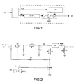
Figure 1 , which receives at its input a modulating signal SM, split up into the amplitude A(t) of the modulating signal and the phase Φ (t) of the modulating signal via, for example, a DSP processor, and which delivers at its output an amplitude-modulated radiofrequency signal RF, i.e. X(t)=A(t) · cos(ω0t+Φ(t)); the polar modulator ofFigure 1 has: - phase modulation carried out according to a synthesizer SYNT,
- amplification of the signal generated by the synthesizer SYNT using a chain of radiofrequency power amplifiers AMP in a saturated class (class AB, B, C, D, E or F) to achieve high efficiency at radiofrequency,
- envelope, i.e. amplitude, modulation introduced through a power converter CP in the final radiofrequency amplifier stage by varying its supply voltage.
- The envelope modulator manages almost all the power absorbed by the transmitter; it is therefore important that its efficiency be very high. Furthermore, the envelope modulator must supply, to the final amplifier stage, a variable voltage having the dynamic range set by the modulating signal A(t).
- Achieving amplitude modulation by varying the supply voltage of the final amplifier stage has been known for at least 70 years, often referred to as "plate modulation ", and was achieved using a modulation transformer (see, for example, "Radio Engineers Handbook", McGraw Hill, 1943).
- The possibility of implementing the amplitude modulator by means of a step-down pulse width modulation regulator, i.e. a "PWM regulator", thereby eliminating the modulation transformer, was introduced at around the end of the 1960s. Today, it is well known both in scientific literature (see, for example, "Polar Modulation-Based RF Power Amplifiers with Enhanced Envelope Processing Technique" by J.K. Jau, F.Y. Han, M.C. Du, T.S. Horng, T.C. Lin at the 34th European Microwave Conference, Amsterdam, 2004) and in patent documentation (see, for example, patents
US 3,413,570 ,US 3,506,920 ,US 3,588,744 ,US 4,896,372 ). - In general, the approach proposed in such literature is always that of a step-down regulator that drives a radiofrequency power amplifier in class AB, B, C, D, E or F or other "saturated" classes, by varying its supply voltage.
- A further advancement was proposed in 1999 by patent
US 6,636,112 in which there is added in cascade with the step-down PWM regulator a linear regulator having a dual functionality: - a) to follow the quicker dynamics of the signal, making up for the problems inherent in the PWM regulator and described later in the present document,
- b) to reduce the noise introduced by the switching in the PWM regulator that normally gives rise to spurious components in the transmitted signal (see patent
US 6,636,112 at column 8, lines 34 to 39). - Such a linear regulator reduces the overall efficiency of the system since, by its nature, it dissipates some of the energy supplied by the PWM regulator (see patent
US 6,636,112 at column 9, lines 7 to 13). - In patent
US 6,636,112 (see at column 8,lines 1 to 14) it is assumed that the resistance exhibited by the final stage at its supply port is constant. - The general aim of the present invention is to eliminate or reduce the drawbacks of the prior art.
- This aim is achieved by the power converter having the characteristics indicated in the accompanying claims which are to be considered an integral part of the present description.
- The present invention is based on the idea of recovering excess energy accumulated at the output using a suitable circuit and, in particular, transferring it to the input.
- A further innovative aspect of the present invention can be appreciated by considering that which is asserted in patent
US 6, 636, 112 at column 8,lines 1 to 14, where it is assumed that the resistance exhibited by the final stage at its supply port is constant. Such an affirmation is true only in the presence of perfectly matched loads and is fundamental in the abovementioned patent to succeed in calculating, independently of everything, the voltage to be applied to the final stage in order to have the desired power. In the solution proposed by the present invention there is no such constraint; the control method allows to calculate (cycle by cycle) the duty cycle to be realized (in order to produce the voltage to be applied to the final stage) even in the presence of a power amplifier whose resistance exhibited at the supply port is variable. The true resistance of the power amplifier can therefore be measured (cycle by cycle) and this value (or an average value thereof) can be used at the next cycle. - With the present invention (by virtue also of the original control method), highly unmatched or variable loads may therefore also be accommodated.
- The invention will now be better explained with the aid of the accompanying drawings, which however are intended only as explanatory and non-limiting examples, in which:
-
Figure 1 shows a block diagram of an amplitude modulation transmitter, -
Figure 2 shows a simplified diagram of a first example embodiment of the converter according to the present invention, -
Figure 3A shows the possible path of a phasor on the I-Q plane, -
Figure 3B shows how the amplitude of the phasor ofFigure 3A varies with time and the corresponding output voltage of a converter, -
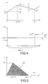
Figure 4 shows how the current I1 varies according to formula [3], and how the voltage Vout varies according to the second assumption on which the analytical model of the present invention is based and in light of formula [4], -
Figure 5 shows a possible manner in which the current I2 can vary and the associated integral Qs calculated according to formula [19], -
Figure 6 shows a simplified diagram of a second example embodiment of the converter according to the present invention, and -
Figure 7 shows a simplified diagram of a third example embodiment of the converter according to the present invention. - To achieve high efficiency, the converter according to the present invention employs the pulse width modulation, or PWM, technique as shown in
Figure 2 ,Figure 6 and Figure 7 . - One of the innovative aspects of the present invention is the combining of two different PWM regulators: the first, made up of an inductor L1, a capacitor C1, a transistor M1 and a diode D1, is a step-down regulator and manages the flow of power from the main electrical power source, i.e. the positive voltage source Vcc, to the load RL, assumed to be substantially resistive; the second, made up of an inductor L2, a transistor M2 and a diode D2, is a step-up regulator and provides a fast discharge of the circuit components L1 and C1, i.e. the two components of the first regulator that store energy.
- In other words the step-up regulator is capable of transferring, without dissipating, energy from the circuit components L1 and C1 to the main source Vcc. To do this sufficiently fast, a secondary electrical power source is preferably used, i.e. the negative voltage source Vdd.
- Naturally, the two PWM regulators and their switching circuit components M1 and M2 are controlled by an appropriate control unit, indicated UC in
Figure 2 ,Figure 6 and Figure 7 ; the component M1 is driven by a switching signal with a duty cycle Dc and the component M2 is driven by a switching signal with a duty cycle Ds. - As regards the switching circuit components, by appropriately choosing the control driver, the transistors M1 and M2 may be N-channel or P-channel MOSFETs, independently of each other, or other types of transistors.
- As regards the diodes D1 and D2, these may be PN junction or Schottky diodes. Furthermore, these diodes could be replaced or put together with transistors, for example, of the MOSFET type suitably driven so as to have a very limited voltage drop across these circuit components during the conduction phases; this contributes to further increasing the efficiency.
- The main generator Vcc must be designed to supply all the power required by the final radiofrequency amplifier stage.
- The step-down regulator, controlled by the signal with duty cycle Dc, transfers power to the output by allowing the output voltage VOUT to vary, as required according to the modulating signal A(t).
- The steady-state response of a step-down regulator is:

where: - Vcc = voltage of the main source;
- VOUT ∈ [0, Vcc] = output voltage;
- Dc ∈ [0,1] = duty cycle.
- The dynamic response is different; this is due to two different physical phenomena:
- the low-pass linear response of the components L1, C1, RL;
- the non-linear response due to the topology of the circuit components M1 and D1 which allows current to flow from Vcc to VOUT but not vice versa.
- The linear behaviour of the step-down regulator can be compensated for by acting on the duty cycle Dc of the signal driving the transistor M1.
- The step-down regulator exhibits its non-linear behaviour when a steep negative slope is required for the output voltage VOUT; in that case neither the transistor M1 nor the diode D1 is capable of removing energy from the inductor L1 and the capacitor C1, and the output voltage falls according to the law RL-C1/L1.
- With reference to
Figure 3B , it is possible to show that the non-linear distortion starts when the (negative) slope of the desired output voltage exceeds the relaxation time of the circuits L1, C1, RL.
- The direct consequence of formula [2] is that the maximum allowable slope tends to zero with the output voltage V0. If the voltage V0 is close to zero, the output resistance RL is not able to quickly discharge the capacitor C1 and as a result the voltage VOUT will turn out to have a (negative) derivative close to zero.
- This result shows the main problem related to the step-down topology: the circuit cannot reproduce waveforms with cusps down to zero.
- A typical example is indicated in
Figure 3 ; in particularFigure 3A shows the path of a phasorX (t) of modulus A(t) and phase Φ(t) which, on the I-Q plane, passes through the origin of the axes; trajectories of this type are common in many modulation schemes (such as QAM, SSB, DSB or others).Figure 3B shows the corresponding variation of the amplitude A(t) of the phasorX (t) and of the actual output voltage VOUT; close to the cusp, the output resistance RL is not able to discharge the capacitor C1 quickly enough and, as a result, VOUT strays from A(t). - The step-up regulator has been included to solve this specific problem. This second regulator, driven by a signal with duty cycle Ds, is for reversing the direction of flow of energy: from the output, or better still from the components L1 and C1, to the main source Vcc.
- The step-up regulator uses a supporting negative voltage source Vdd to increase the speed of discharge of the output circuit. Thus, this modulator can follow both the fast dynamics of the modulating signal and the passage through zero, and the approaching to zero with non-zero derivative of the modulating signal.
- Furthermore, the step-up regulator, by enabling excess energy at the output to be removed by transferring it to the main generator Vcc, keeps the overall efficiency high.
- The use of step-down and step-up PWM regulators to vary the voltage VOUT results in high efficiency and high dynamics but introduces noise at the switching frequency and at its harmonics. This noise can be seen by the presence of spurious components in the amplitude modulation (at the switching frequency and at its harmonics) with possible problems in terms of "adjacent-channel noise".
- The switching frequency must be (according to the Nyquist theorem) at least twice the maximum bandwidth of the modulating signal; the result is that the problem of transmission of spurious components does not affect the in-band signal but rather the adjacent channels.
- To solve this problem, the present invention considers two different approaches.
- The first approach consists in removing the unwanted frequencies (the switching frequency fsw and its harmonics 2 fsw, 3 fsw, ...) using a multiple notch filter.
- The variation in phase introduced by this filter, at the envelope frequencies of the modulator, will be considered as part of the total phase lag between A(t) and VOUT.
- The notch filter will have a structure that minimizes the equivalent capacitance in relation to ground, since it will be added to the capacitance of the capacitor C1, and it is the main component responsible for the non-linear distortions previously described.
- In
Figure 2 ,Figure 6 and Figure 7 , the multiple notch filter is labelled F. - The second approach consists in spreading the unwanted frequencies by applying a random and variable time-domain jitter to the switching and therefore causing the duration T of the switching period to vary slightly and continuously in a random manner.
- This solution, simple from the circuit point of view, increases the complexity of the control unit UC (see
Figure 2 ,Figure 6 and Figure 7 ) not only through the introduction of a random generator but also because in the control algorithm formulae the duration of the switching period becomes a variable. - It is to be noted that these two approaches may advantageously be used in combination.
- From the control point of view, the system can be considered as having two inputs, i.e. the duty cycles Dc and Ds, and one output, i.e. the output voltage VOUT. An analytical model has therefore been developed intended to be used for a digital electronic control.
- This model calculates the value of the output voltage VOUT as a function of the duty cycle Dc at the end of each switching cycle. This model can easily be inverted, providing the duty cycle Dc as a function of the output voltage VOUT. The acceptable range of values for Dc is between 0 and 1; if the calculated value of Dc is less than zero, the algorithm calculates the duty cycle Ds, which ensures the desired output voltage.
- With reference to
Figure 2 , the following six assumptions are made. - According to the first assumption, the voltage V0 across the capacitor C1 is equal to the output voltage VOUT in the band of A(t). Such an assumption is justified by the notch structure of the output filter which therefore does not substantially attenuate signals in the band of the modulating signal.
- According to the second assumption, the voltage V0 across the capacitor C1 is constant during each switching cycle.
- According to the third assumption, the power amplifier is modelled as a resistor of value RL. In the disclosure that follows, the resistance RL will be assumed to be constant in each switching cycle. If therefore the power amplifier is modelled with a characteristic RL = RL (VOUT), possible non-linear behaviour of the amplifier may also be taken into account in the model. In that case, the following expression can be used: RL (n) -RL(VOUT (n)).
- According to the fourth assumption, the threshold voltage of the diode D1 and the diode D2 is assumed to be zero.
- According to the fifth assumption, the current I2 that flows through the inductor L2 is zero at the end of each switching cycle. This choice has been made by considering that the energy flow is mainly directed from the source Vcc to the load RL and only in some particular cases in the reverse direction.
- Thus two advantages arise.
- The first advantage is related to the fact that there would only be two (instead of three) state variables for the system, since two are the components that store energy from one cycle to the next, namely the inductor L1 and the capacitor C1.
- The second advantage is related to the fact that energy loops are thus avoided by design. In other words, the undesired condition in which energy is taken from the source Vcc, transferred to the output (by the step-down regulator) and then returned (by the step-up regulator) to the source Vcc never arises.
- According to the sixth assumption, the variation in the duty cycle Dc from one switching cycle to the next is small compared with the said duty cycle.
- The model uses two relationships:
- the continuity of the current I1 through the inductor L1, represented by formula [3] below, and
- the preservation of the charge on the capacitor C1, represented by formula [4] below.


-
Figure 4 shows how the current I1 varies and how the voltage Vout varies, according to the assumption made. By substituting in formulae [3] and [4] the following formulae [5], [6] and [7]:


where


- Formulae [8] and [9] represent a simplified, but very effective, model of the step-down PWM regulator and allow to calculate the voltage V0 across the capacitor C1 (which corresponds to the output voltage VOUT) and the current I1 flowing through the inductor L1 at cycle "n+1" on the basis of the values of the current I1, voltage VOUT, duty cycle Dc and duration T of the switching period at cycle "n".
- Based on this analytical model, effective control methods can be implemented for controlling the switching components of the PWM regulators included in the power converter according to the present invention.
- A first control method is based purely on the analytical model of formulae [8] and [9]; the simplified diagram of the associated converter is shown in
Figure 2 . - The problem that needs to be solved is to calculate which duty cycle Dc has to be applied to cycle "n" (Dc (n) in
Figure 4 ), with VOUT (n+1) (new target voltage), VOUT (n) and I1 (n) (present values of the two state variables of the system), and T(n) being known. - Therefore formula [9] needs to be processed, expressing the duty cycle Dc as a function of all the remainder. The problem is the non-linearity of formula [9] with respect to the duty cycle Dc.
- Rather than solving a quadratic equation, with complicated processing and which would require a complex logic circuit, the sixth assumption mentioned previously is exploited together with the fact that the variation in the term (1-Dc (n)/2) is definitely less than the variation in Dc (both present in the second term of formula [9]).
- Therefore, this leads to:

- Formula [10] is the one which allows to obtain the duty cycle Dc to be realized at cycle "n" to obtain the voltage VOUT (n+1), with the values VOUT (n), I1 (n) and Dc (n-1) being known.
The logic control unit UC must therefore calculate, at each cycle, the following pair of formulae, and specifically formula [11] first followed by formula [12]:

- Considering that the current I1 cannot reverse its direction, formula [12] must be saturated at zero, i.e.: if I1 (n+1) < 0 => I1 (n+1) =0
- The result of formula [11], however, may be positive or negative, but a negative duty cycle does not have any physical meaning. In that case, the model is indicating that to reach the target voltage VOUT (n+1), charge would need to be taken away from C1, and this can be achieved by setting Dc=0 and Ds>0.
- Formulae [8] and [9] of the model, in that case, will continue to be valid, setting Dc (n)=0 and with the addition of a quantity of charge Qs (n) which must be removed from C1; therefore, it is:


- In the cycle in question, the charge Qs (n) to be removed from C1 to obtain VOUT (n+1) can therefore be calculated as:

- It is noted that formula [15], apart from the scale factor "-C1", corresponds to the numerator of formula [11] and therefore does not need to be recalculated. If therefore at cycle "n" the result is Dc<0, then Dc=0 must be imposed and the charge to be removed from the capacitor C1 must be calculated on the basis of formula [15] (which charge is definitely positive since the denominator of formula [11] is definitely positive).
- At this point, by also exploiting the fifth assumption previously mentioned, the duty cycle Ds (n) may be calculated from the charge Qs (n) (refer to
Figure 5 for a better understanding).

- By equalizing formulae [16] and [17], the instant at which the current I2 returns to zero can be calculated, corresponding to DOFF (n) T(n) :

- The constraint imposed by the fifth assumption previously mentioned is reflected in the maximum value of DOFF (n), which must be equal to 1. It follows that Ds (n) cannot exceed a certain value which we will indicate DsMAX (n):

- Qs (n) can now be calculated as a function of Ds (n) :

- By equalizing formulae [15] and [19] and expressing Ds (n), we obtain:

- In conclusion, the algorithm for calculating Dc (n) and Ds (n) is as follows.
- Step 1 (first method) :

- Step 2 (first method) :
- If N(n)≥0

- If N(n) <0

- If N(n)≥0
- Step 3 (first method):

- Step 4 (first method) :
- if Ic ≥0 => I1 (n+1)= Ic;
if Ic <0 => I1 (n+1)= 0.
- if Ic ≥0 => I1 (n+1)= Ic;
- Formula [23] is the most difficult to be calculated by dedicated logic circuitry, because of the presence of the term (Vcc-VOUT (n))/(Vdd+VOUT (n)) and because of the square root.
- Given that the discharge (and therefore the calculation of formula [23]) takes place normally when VOUT (n) is small, the following approximation can be applied:

- A second control method is based on the analytical model of formulae [8] and [9], but instead of obtaining I1 (n) from the model and assuming that the VOUT (n) requested is actually that obtained, it measures these two quantities.
- The simplified diagram of the associated converter is shown in
Figure 6 ; this differs from the diagram ofFigure 2 by the addition of two circuit components ADC, analogue-to-digital converters, to carry out the measurements. - This second method exhibits the following advantages:
- lower complexity in the algorithm since the calculations related to steps 3 and 4 illustrated previously are avoided,
- possibility of including protective measures against excess currents or excess voltages,
- more accurate control during the start transient, when the current I1 of the model is not stable enough yet.
- Naturally, it is necessary to provide the circuitry needed to measure the abovementioned quantities.
- The idea is to make use of the measured quantities not for a closed loop control in the conventional sense, but as initial values for cycle "n" in order to calculate, by means of the model, the duty cycle.
- With


- Step 1 (second method) :

where VOUT (n+1) is the next value of the output voltage as a consequence of the input A(t). - Step 2 (second method) :
- If N(n) ≥0

- If N(n) <0

- If N(n) ≥0
- A third control method is based on the analytical model of formulae [8] and [9], but it needs the measurement of the output voltage VOUT and the determination of the load applied at the output, in particular the actual value of the resistive load RL.
- In the example of
Figure 7 , the load is determined by measuring the output current I0; the ratio between the measured value of the voltage VOUT and the measured value of the current Io corresponds to the resistance value of the load. - The load can be determined in other ways, for example by measuring the power transferred to the load or by measuring the converter input current and estimating the output of the converter.
- A simplified diagram of a converter based on this method is shown in
Figure 7 ; this differs from the diagram ofFigure 2 by the addition of two circuit components ADC, analogue-to-digital converters, to carry out the measurements. - The true resistance of the power amplifier, in particular of its output stage, can therefore be worked out (cycle by cycle, if this is desired) and the said value (or an average value thereof) can be used at the next cycle to precisely calculate the duty cycle needed to obtain the desired power.
- With


- Step 1 (third method):

where VOUT (n+1) is the next value of the output voltage as a consequence of the input A(t); I1 (n) is the value of the current through the inductor L1 calculated using the model;
- Step 2 (third method):
- If N(n), ≥0

- If N(n) <0

- If N(n), ≥0
- Step 3 (third method):

- Step 4 (third method):
- if Ic 20 => I1 (n+1)= Ic;
- if Ic <0 => I1 (n+1)=0.
- The diagrams of
Figure 2 ,Figure 6 and Figure 7 are fairly complete, but simplified; for example, the MOSFET transistor driver circuits are not elaborated; also, for example, the circuitry that generates the voltage signals to be sent to the circuit components ADC is represented only in an indicative manner: in the case of determination of a voltage signal, it is reduced to a single wire, while in the case of determination of a current signal it is reduced to a resistor, namely the resistor Rs. - In practice, for example, it will be necessary to include circuits for adapting the voltage signal to be sampled to the dynamic range of the analogue input voltage of the specific circuit components ADC chosen; in the case of detecting the current signal, a suitable current-voltage converter must be chosen.
- Furthermore, the signals detected must be suitably filtered (anti-aliasing filter) so as not to allow the harmonics and other frequencies, outside the band of the circuit components ADC, to be sampled.
- Finally, a clock signal must be supplied to the circuit components ADC, at the desired sampling frequency.
- It is worth noting that, in these diagrams, both the PWM converters are connected directly to each other; however, one cannot rule out that this connection might be made indirectly via other circuit components not represented in these diagrams.
- For completeness, a list of components that can be used in these circuits is set out below in table form.
Circuit component Manufacturer Component identification M1 INTERNATIONAL RECTIFIER IRLR9343 D1 INTERNATIONAL RECTIFIER 50WQ10FN L1 PULSE ENGINEERING PE-54044S C1 TERN MURATA MANUFACTURING 3 x 330nF in parallel M2 INTERNATIONAL RECTIFIER IRLR3105 L2 COILCRAFT 4.7uH D2 INTERNATIONAL RECTIFIER 50WQ10FN XILINX XC2S150E UC + UNITRODE UC2715 ADC ANALOG DEVICES AD7894 - Clearly, various modifications can be introduced to that which has been described and illustrated, by way of example, and the means or materials described can be replaced by equivalent means or materials without consequently departing from the claimed scope of protection.
Claims (12)
- Power converter adapted to be connected to an electrical power source and manage the flow of power from said source to a load, the converter receiving at its input a control signal (A(t)) for the conversion and being characterised in that it includes:- a first regulator circuit (L1, C1, M1, D1) of the pulse width modulation step-down type, which is adapted to be connected to a positive voltage source (Vcc) and referred to ground so as to provide a positive voltage output;- an energy recovery circuit, including a second regulator circuit (L2, M2, D2) of the pulse width modulation step-up type, connected to said first regulator circuit (L1, C1, M1, D1), which is adapted to be connected to a supporting negative voltage source (Vdd), so as to quickly discharge energy-storing circuit components (L1, C1) of the said first regulator circuit (L1, C1, M1, D1),wherein:- the input of the said second regulator circuit (L2, M2, D2) is connected to the output of the said first regulator circuit (L1, C1, M1, D1) and the output of the said second regulator circuit (L2, M2, D2) is connected to the input of the said first regulator circuit (L1, C1, M1, D1),- the first regulator circuit includes a series switching element (M1), a shunt diode to ground (D1), a series inductance (L1) and a shunt capacitor to ground (C1),- the second regulator circuit includes a series inductance (L2), a shunt switching element (M2) connected to the supporting negative voltage source (Vdd), and a freewheeling diode (D2) to the positive voltage source (Vcc),
the switching component (M1) of the first regulator circuit being driven by a switching signal with a first duty cycle (Dc) and the switching component (M2) of the second regulator circuit being driven by a switching signal with a second duty cycle (Ds); and- a control unit (UC) for switching circuit components (M1, M2) of the said first (L1, C1, M1, D1) and second regulator circuit (L2, M2, D2), which is arranged to control the switching of the said components (M1, M2) and to determine the said duty cycles (Dc, Ds) so as they do not overlap in time, in relation to the said control signal (A(t)), according to a predetermined feed-forward control method based on an open-loop analytical model of the said first regulator circuit (L1, C1, M1, D1). - Power converter according to Claim 1, in which the said control unit (UC) is arranged to set the width (Dc, Ds) of the switching pulses periodically, at each switching cycle.
- Power converter according to Claim 2, characterized in that the said control unit (UC) is arranged to set the width (Dc, Ds) of the switching pulses also in relation to the previous state at least of the said first regulator circuit (L1, C1, M1, D1), in particular the state at the previous switching cycle.
- Power converter according to one of Claims 1 to 3, characterized in that the said control unit (UC) is adapted to apply a random and variable time-domain jitter to the switching of the said switching circuit components.
- Power converter according to any of the preceding claims, characterized in that it includes filter means (F) connected downstream of the said first regulator circuit (L1, C1, M1, D1) and adapted to filter out the switching noise.
- Power converter according to Claim 5, characterized in that the said filter means (F) comprise a multiple notch filter.
- Power converter according to any of the preceding claims, characterized in that it includes means (ADC) adapted to determine at least some of the state variables (I1, Vo) of the said first regulator circuit (L1, C1, M1, D1), and in that the said control unit (UC) is connected to the said determination means (ADC) and is adapted to operate according to a control method, based on the analytical model of the first regulator circuit (L1, C1, M1, D1), that takes into account the values of the state variables (I1, Vo) determined.
- Power converter according to any of the preceding claims, characterized in that it includes determination means (ADC) adapted to detect the output voltage (Vout) at the converter and the load (RL) applied at the output of the converter, and in which the said control unit (UC) is connected to the said determination means (ADC) and is adapted to operate according to a control method, based on the analytical model of the first regulator circuit (L1, C1, M1, D1), that takes into account the output voltage (Vout) determined and the load on the output (RL) determined.
- Power converter according to Claim 8, in which the said determination means (ADC) are adapted to measure the output voltage (Vout) at the converter and the output current (Io) at the converter.
- Power converter according to one of the preceding claims, characterized in that it is adapted to power any type of load or actuator.
- Amplitude modulator adapted to receive at the input a modulating signal and including an amplifier and a power supplier adapted to supply power, characterized in that the said power supplier includes a power converter according to one of the preceding claims, whose control signal (A(t)) for the conversion corresponds to the said modulating signal.
- Radio transmitter including an amplitude modulator according to the preceding claim.
Applications Claiming Priority (2)
| Application Number | Priority Date | Filing Date | Title |
|---|---|---|---|
| IT000402A ITTO20050402A1 (en) | 2005-06-10 | 2005-06-10 | HIGH EFFICIENCY POWER CONVERTER, MODULATOR AND TRANSMITTER USING IT |
| PCT/IB2006/051827 WO2006131896A2 (en) | 2005-06-10 | 2006-06-08 | High efficiency power converter, and modulator and transmitter using it |
Publications (2)
| Publication Number | Publication Date |
|---|---|
| EP1894289A2 EP1894289A2 (en) | 2008-03-05 |
| EP1894289B1 true EP1894289B1 (en) | 2009-11-04 |
Family
ID=37498825
Family Applications (1)
| Application Number | Title | Priority Date | Filing Date |
|---|---|---|---|
| EP06756087A Active EP1894289B1 (en) | 2005-06-10 | 2006-06-08 | High efficiency power converter, and modulator and transmitter using it |
Country Status (12)
| Country | Link |
|---|---|
| US (1) | US20100270986A1 (en) |
| EP (1) | EP1894289B1 (en) |
| AT (1) | ATE447789T1 (en) |
| CA (1) | CA2611634C (en) |
| DE (1) | DE602006010201D1 (en) |
| DK (1) | DK1894289T3 (en) |
| ES (1) | ES2335690T3 (en) |
| IT (1) | ITTO20050402A1 (en) |
| NO (1) | NO336955B1 (en) |
| RU (1) | RU2380818C2 (en) |
| UA (1) | UA90434C2 (en) |
| WO (1) | WO2006131896A2 (en) |
Families Citing this family (5)
| Publication number | Priority date | Publication date | Assignee | Title |
|---|---|---|---|---|
| CN104192014B (en) * | 2014-09-05 | 2016-05-04 | 江苏今创车辆有限公司 | Adopt the battery trolley locomotive of unified Voltage-output and two-way DC/DC module |
| US11863062B2 (en) * | 2018-04-27 | 2024-01-02 | Raytheon Company | Capacitor discharge circuit |
| KR102274958B1 (en) * | 2019-04-15 | 2021-07-08 | 주식회사 에스제이솔루션 | Power Supply Unit Using Intellectual Pre-Regulator |
| WO2021091564A1 (en) * | 2019-11-07 | 2021-05-14 | Hewlett-Packard Development Company, L.P. | Snubber circuit |
| CN119469206B (en) * | 2024-11-19 | 2025-11-07 | 湖南航天机电设备与特种材料研究所 | Portable gyroscope shake driving measurement system and method |
Family Cites Families (16)
| Publication number | Priority date | Publication date | Assignee | Title |
|---|---|---|---|---|
| US3506920A (en) * | 1966-02-10 | 1970-04-14 | Gates Radio Co | High efficiency transformer utilizing pulse duration modulation to eliminate audio-rf transformer coupling |
| US3413570A (en) * | 1966-02-23 | 1968-11-26 | Collins Radio Co | High efficiency rf power amplification with modulation signal controlled "on"-"off" switch varied amplifier dc potentials |
| US3588744A (en) * | 1969-11-07 | 1971-06-28 | Gates Radio Co | Amplitude compensated pulse duration modulator |
| US4896372A (en) * | 1986-02-25 | 1990-01-23 | Varian Associates, Inc. | Pulse width modulator for AM-RF transmitter |
| JP3238833B2 (en) * | 1994-10-07 | 2001-12-17 | 富士通株式会社 | Power supply circuit |
| US5657219A (en) * | 1995-08-29 | 1997-08-12 | Crown International, Inc. | Opposed current power converter |
| US6198347B1 (en) * | 1999-07-29 | 2001-03-06 | Tropian, Inc. | Driving circuits for switch mode RF power amplifiers |
| US6094035A (en) * | 1999-08-20 | 2000-07-25 | Gain Technology Corporation | Amplifying power converter circuits |
| US6348781B1 (en) * | 2000-12-11 | 2002-02-19 | Motorola, Inc. | Buck or boost power converter |
| TWI264172B (en) * | 2001-08-29 | 2006-10-11 | Oqo Inc | Bi-directional DC power conversion system |
| US20030174005A1 (en) * | 2002-03-14 | 2003-09-18 | Latham Paul W. | Cmos digital pulse width modulation controller |
| KR100476202B1 (en) * | 2002-06-25 | 2005-03-10 | 현대자동차주식회사 | A method for preventing and diagnosing an arm-short of bi-directional dc/dc converter |
| US6977492B2 (en) * | 2002-07-10 | 2005-12-20 | Marvell World Trade Ltd. | Output regulator |
| TW200513013A (en) * | 2003-09-26 | 2005-04-01 | Asustek Comp Inc | Active clamping circuit and power supply system using the same |
| US6977827B2 (en) * | 2004-03-22 | 2005-12-20 | American Superconductor Corporation | Power system having a phase locked loop with a notch filter |
| US7157888B2 (en) * | 2005-06-06 | 2007-01-02 | Aimtron Technology Corp. | Light loading control circuit for a buck-boost voltage converter |
-
2005
- 2005-06-10 IT IT000402A patent/ITTO20050402A1/en unknown
-
2006
- 2006-06-08 DK DK06756087.0T patent/DK1894289T3/en active
- 2006-06-08 ES ES06756087T patent/ES2335690T3/en active Active
- 2006-06-08 DE DE602006010201T patent/DE602006010201D1/en active Active
- 2006-06-08 EP EP06756087A patent/EP1894289B1/en active Active
- 2006-06-08 UA UAA200800329A patent/UA90434C2/en unknown
- 2006-06-08 US US11/917,146 patent/US20100270986A1/en not_active Abandoned
- 2006-06-08 AT AT06756087T patent/ATE447789T1/en active
- 2006-06-08 WO PCT/IB2006/051827 patent/WO2006131896A2/en not_active Ceased
- 2006-06-08 RU RU2008100033/09A patent/RU2380818C2/en active
- 2006-06-08 CA CA2611634A patent/CA2611634C/en active Active
-
2008
- 2008-01-09 NO NO20080149A patent/NO336955B1/en unknown
Also Published As
| Publication number | Publication date |
|---|---|
| WO2006131896A2 (en) | 2006-12-14 |
| CA2611634A1 (en) | 2006-12-14 |
| US20100270986A1 (en) | 2010-10-28 |
| ATE447789T1 (en) | 2009-11-15 |
| ES2335690T3 (en) | 2010-03-31 |
| DK1894289T3 (en) | 2010-03-22 |
| RU2380818C2 (en) | 2010-01-27 |
| NO20080149L (en) | 2008-02-19 |
| UA90434C2 (en) | 2010-04-26 |
| RU2008100033A (en) | 2009-07-20 |
| DE602006010201D1 (en) | 2009-12-17 |
| ITTO20050402A1 (en) | 2006-12-11 |
| EP1894289A2 (en) | 2008-03-05 |
| WO2006131896A3 (en) | 2007-10-11 |
| CA2611634C (en) | 2014-08-19 |
| NO336955B1 (en) | 2015-11-30 |
Similar Documents
| Publication | Publication Date | Title |
|---|---|---|
| US10770969B2 (en) | Digital average current-mode control voltage regulator and a method for tuning compensation coefficients thereof | |
| Kim et al. | A 10-MHz 2–800-mA 0.5–1.5-V 90% peak efficiency time-based buck converter with seamless transition between PWM/PFM modes | |
| US8729871B2 (en) | Circuit and method for controlling the power supply of a consumer with current pulses having steep flanks | |
| EP1632827A1 (en) | Control circuit for current mode buck converter | |
| US20170302172A1 (en) | A voltage regulator module using a load-side auxiliary gyrator circuit | |
| Su et al. | Gain scheduling control scheme for improved transient response of DC/DC converters | |
| WO1999031790A1 (en) | Discrete-time sampling of data for use in switching regulators | |
| US9716954B2 (en) | DC impedance detection circuit and method for speaker | |
| US20130063113A1 (en) | Load current sensing circuit and method | |
| US10985655B1 (en) | Peak current limit in a slope-compensated current mode DC-DC converter | |
| US8901910B2 (en) | System and method of predictive current feedback for switched mode regulators | |
| Wittmann et al. | MHz-converter design for high conversion ratio | |
| US20100270986A1 (en) | High efficiency power converter, and modulator and transmitter using it | |
| US10340796B2 (en) | Constant on time boost converter control | |
| Milanovic et al. | FPGA implementation of digital controller for DC-DC buck converter | |
| CN113949249B (en) | Electronic device comprising a switching output stage, corresponding circuit arrangement and method | |
| US10038381B2 (en) | Area-friendly method for providing duty cycle inverse to supply voltage | |
| WO2010118990A1 (en) | Analogue conversion of pulse width modulated signals | |
| EP2482433A2 (en) | Switched DC/DC boost power stage with linear control-to-output conversion ratio, based on a ramp-modulated PWM generator | |
| Padhee et al. | Design and performance analysis of controlled dc-dc converter | |
| Berger et al. | Unified digital sliding mode control with inductor current ripple reconstruction for DC-DC converters | |
| US20230155471A1 (en) | Methods and Systems for Current Sensing in Power Converters | |
| Cheng et al. | Multiphase buck converter with minimum time control strategy for RF envelope modulation | |
| KR100755954B1 (en) | Solar cell system with digital maximum power tracker and its control method | |
| US12160170B2 (en) | Power factor correction system |
Legal Events
| Date | Code | Title | Description |
|---|---|---|---|
| PUAI | Public reference made under article 153(3) epc to a published international application that has entered the european phase |
Free format text: ORIGINAL CODE: 0009012 |
|
| 17P | Request for examination filed |
Effective date: 20080110 |
|
| AK | Designated contracting states |
Kind code of ref document: A2 Designated state(s): AT BE BG CH CY CZ DE DK EE ES FI FR GB GR HU IE IS IT LI LT LU LV MC NL PL PT RO SE SI SK TR |
|
| AX | Request for extension of the european patent |
Extension state: AL BA HR MK YU |
|
| RAX | Requested extension states of the european patent have changed |
Extension state: AL Extension state: BA Extension state: HR Extension state: RS Extension state: MK |
|
| DAX | Request for extension of the european patent (deleted) | ||
| GRAP | Despatch of communication of intention to grant a patent |
Free format text: ORIGINAL CODE: EPIDOSNIGR1 |
|
| GRAS | Grant fee paid |
Free format text: ORIGINAL CODE: EPIDOSNIGR3 |
|
| GRAA | (expected) grant |
Free format text: ORIGINAL CODE: 0009210 |
|
| AK | Designated contracting states |
Kind code of ref document: B1 Designated state(s): AT BE BG CH CY CZ DE DK EE ES FI FR GB GR HU IE IS IT LI LT LU LV MC NL PL PT RO SE SI SK TR |
|
| REG | Reference to a national code |
Ref country code: GB Ref legal event code: FG4D |
|
| REG | Reference to a national code |
Ref country code: CH Ref legal event code: EP |
|
| REG | Reference to a national code |
Ref country code: RO Ref legal event code: EPE |
|
| REG | Reference to a national code |
Ref country code: IE Ref legal event code: FG4D |
|
| REF | Corresponds to: |
Ref document number: 602006010201 Country of ref document: DE Date of ref document: 20091217 Kind code of ref document: P |
|
| REG | Reference to a national code |
Ref country code: SE Ref legal event code: TRGR |
|
| REG | Reference to a national code |
Ref country code: GR Ref legal event code: EP Ref document number: 20100400160 Country of ref document: GR |
|
| REG | Reference to a national code |
Ref country code: DK Ref legal event code: T3 |
|
| REG | Reference to a national code |
Ref country code: ES Ref legal event code: FG2A Ref document number: 2335690 Country of ref document: ES Kind code of ref document: T3 |
|
| NLV1 | Nl: lapsed or annulled due to failure to fulfill the requirements of art. 29p and 29m of the patents act | ||
| LTIE | Lt: invalidation of european patent or patent extension |
Effective date: 20091104 |
|
| PG25 | Lapsed in a contracting state [announced via postgrant information from national office to epo] |
Ref country code: PT Free format text: LAPSE BECAUSE OF FAILURE TO SUBMIT A TRANSLATION OF THE DESCRIPTION OR TO PAY THE FEE WITHIN THE PRESCRIBED TIME-LIMIT Effective date: 20100304 Ref country code: LT Free format text: LAPSE BECAUSE OF FAILURE TO SUBMIT A TRANSLATION OF THE DESCRIPTION OR TO PAY THE FEE WITHIN THE PRESCRIBED TIME-LIMIT Effective date: 20091104 Ref country code: IS Free format text: LAPSE BECAUSE OF FAILURE TO SUBMIT A TRANSLATION OF THE DESCRIPTION OR TO PAY THE FEE WITHIN THE PRESCRIBED TIME-LIMIT Effective date: 20100304 |
|
| PG25 | Lapsed in a contracting state [announced via postgrant information from national office to epo] |
Ref country code: SI Free format text: LAPSE BECAUSE OF FAILURE TO SUBMIT A TRANSLATION OF THE DESCRIPTION OR TO PAY THE FEE WITHIN THE PRESCRIBED TIME-LIMIT Effective date: 20091104 Ref country code: CY Free format text: LAPSE BECAUSE OF FAILURE TO SUBMIT A TRANSLATION OF THE DESCRIPTION OR TO PAY THE FEE WITHIN THE PRESCRIBED TIME-LIMIT Effective date: 20091104 Ref country code: LV Free format text: LAPSE BECAUSE OF FAILURE TO SUBMIT A TRANSLATION OF THE DESCRIPTION OR TO PAY THE FEE WITHIN THE PRESCRIBED TIME-LIMIT Effective date: 20091104 Ref country code: PL Free format text: LAPSE BECAUSE OF FAILURE TO SUBMIT A TRANSLATION OF THE DESCRIPTION OR TO PAY THE FEE WITHIN THE PRESCRIBED TIME-LIMIT Effective date: 20091104 |
|
| REG | Reference to a national code |
Ref country code: HU Ref legal event code: AG4A Ref document number: E007323 Country of ref document: HU |
|
| PG25 | Lapsed in a contracting state [announced via postgrant information from national office to epo] |
Ref country code: EE Free format text: LAPSE BECAUSE OF FAILURE TO SUBMIT A TRANSLATION OF THE DESCRIPTION OR TO PAY THE FEE WITHIN THE PRESCRIBED TIME-LIMIT Effective date: 20091104 |
|
| PG25 | Lapsed in a contracting state [announced via postgrant information from national office to epo] |
Ref country code: SK Free format text: LAPSE BECAUSE OF FAILURE TO SUBMIT A TRANSLATION OF THE DESCRIPTION OR TO PAY THE FEE WITHIN THE PRESCRIBED TIME-LIMIT Effective date: 20091104 |
|
| PLBE | No opposition filed within time limit |
Free format text: ORIGINAL CODE: 0009261 |
|
| STAA | Information on the status of an ep patent application or granted ep patent |
Free format text: STATUS: NO OPPOSITION FILED WITHIN TIME LIMIT |
|
| 26N | No opposition filed |
Effective date: 20100805 |
|
| PG25 | Lapsed in a contracting state [announced via postgrant information from national office to epo] |
Ref country code: MC Free format text: LAPSE BECAUSE OF NON-PAYMENT OF DUE FEES Effective date: 20100630 |
|
| REG | Reference to a national code |
Ref country code: CH Ref legal event code: PL |
|
| PG25 | Lapsed in a contracting state [announced via postgrant information from national office to epo] |
Ref country code: IT Free format text: LAPSE BECAUSE OF FAILURE TO SUBMIT A TRANSLATION OF THE DESCRIPTION OR TO PAY THE FEE WITHIN THE PRESCRIBED TIME-LIMIT Effective date: 20091104 |
|
| PG25 | Lapsed in a contracting state [announced via postgrant information from national office to epo] |
Ref country code: IE Free format text: LAPSE BECAUSE OF NON-PAYMENT OF DUE FEES Effective date: 20100608 Ref country code: CH Free format text: LAPSE BECAUSE OF NON-PAYMENT OF DUE FEES Effective date: 20100630 Ref country code: LI Free format text: LAPSE BECAUSE OF NON-PAYMENT OF DUE FEES Effective date: 20100630 |
|
| PG25 | Lapsed in a contracting state [announced via postgrant information from national office to epo] |
Ref country code: LU Free format text: LAPSE BECAUSE OF NON-PAYMENT OF DUE FEES Effective date: 20100608 Ref country code: NL Free format text: LAPSE BECAUSE OF FAILURE TO SUBMIT A TRANSLATION OF THE DESCRIPTION OR TO PAY THE FEE WITHIN THE PRESCRIBED TIME-LIMIT Effective date: 20091104 |
|
| REG | Reference to a national code |
Ref country code: FR Ref legal event code: PLFP Year of fee payment: 11 |
|
| REG | Reference to a national code |
Ref country code: FR Ref legal event code: PLFP Year of fee payment: 12 |
|
| REG | Reference to a national code |
Ref country code: FR Ref legal event code: PLFP Year of fee payment: 13 |
|
| PGFP | Annual fee paid to national office [announced via postgrant information from national office to epo] |
Ref country code: DE Payment date: 20240627 Year of fee payment: 19 |
|
| PGFP | Annual fee paid to national office [announced via postgrant information from national office to epo] |
Ref country code: DK Payment date: 20240625 Year of fee payment: 19 |
|
| PGFP | Annual fee paid to national office [announced via postgrant information from national office to epo] |
Ref country code: GR Payment date: 20240627 Year of fee payment: 19 |
|
| PGFP | Annual fee paid to national office [announced via postgrant information from national office to epo] |
Ref country code: CZ Payment date: 20240522 Year of fee payment: 19 Ref country code: AT Payment date: 20240521 Year of fee payment: 19 |
|
| PGFP | Annual fee paid to national office [announced via postgrant information from national office to epo] |
Ref country code: RO Payment date: 20240528 Year of fee payment: 19 Ref country code: FI Payment date: 20240625 Year of fee payment: 19 Ref country code: BG Payment date: 20240610 Year of fee payment: 19 |
|
| PGFP | Annual fee paid to national office [announced via postgrant information from national office to epo] |
Ref country code: TR Payment date: 20240523 Year of fee payment: 19 Ref country code: HU Payment date: 20240528 Year of fee payment: 19 Ref country code: BE Payment date: 20240627 Year of fee payment: 19 |
|
| PGFP | Annual fee paid to national office [announced via postgrant information from national office to epo] |
Ref country code: ES Payment date: 20240701 Year of fee payment: 19 |
|
| PGFP | Annual fee paid to national office [announced via postgrant information from national office to epo] |
Ref country code: GB Payment date: 20250627 Year of fee payment: 20 |
|
| PGFP | Annual fee paid to national office [announced via postgrant information from national office to epo] |
Ref country code: FR Payment date: 20250625 Year of fee payment: 20 |
|
| PGFP | Annual fee paid to national office [announced via postgrant information from national office to epo] |
Ref country code: SE Payment date: 20250627 Year of fee payment: 20 |
|
| REG | Reference to a national code |
Ref country code: DE Ref legal event code: R119 Ref document number: 602006010201 Country of ref document: DE |
|
| PG25 | Lapsed in a contracting state [announced via postgrant information from national office to epo] |
Ref country code: FI Free format text: LAPSE BECAUSE OF NON-PAYMENT OF DUE FEES Effective date: 20250608 |
|
| PG25 | Lapsed in a contracting state [announced via postgrant information from national office to epo] |
Ref country code: CZ Free format text: LAPSE BECAUSE OF NON-PAYMENT OF DUE FEES Effective date: 20250608 |
|
| PG25 | Lapsed in a contracting state [announced via postgrant information from national office to epo] |
Ref country code: BG Free format text: LAPSE BECAUSE OF NON-PAYMENT OF DUE FEES Effective date: 20250608 |
|
| PG25 | Lapsed in a contracting state [announced via postgrant information from national office to epo] |
Ref country code: RO Free format text: LAPSE BECAUSE OF NON-PAYMENT OF DUE FEES Effective date: 20250608 |
|
| REG | Reference to a national code |
Ref country code: DK Ref legal event code: EBP Effective date: 20250630 |
|
| REG | Reference to a national code |
Ref country code: AT Ref legal event code: MM01 Ref document number: 447789 Country of ref document: AT Kind code of ref document: T Effective date: 20250608 |
|
| PG25 | Lapsed in a contracting state [announced via postgrant information from national office to epo] |
Ref country code: HU Free format text: LAPSE BECAUSE OF NON-PAYMENT OF DUE FEES Effective date: 20250609 |
|
| REG | Reference to a national code |
Ref country code: BE Ref legal event code: MM Effective date: 20250630 |
|
| PG25 | Lapsed in a contracting state [announced via postgrant information from national office to epo] |
Ref country code: DE Free format text: LAPSE BECAUSE OF NON-PAYMENT OF DUE FEES Effective date: 20260101 |
|
| PG25 | Lapsed in a contracting state [announced via postgrant information from national office to epo] |
Ref country code: AT Free format text: LAPSE BECAUSE OF NON-PAYMENT OF DUE FEES Effective date: 20250608 |
|
| PG25 | Lapsed in a contracting state [announced via postgrant information from national office to epo] |
Ref country code: BE Free format text: LAPSE BECAUSE OF NON-PAYMENT OF DUE FEES Effective date: 20250630 |
|
| PG25 | Lapsed in a contracting state [announced via postgrant information from national office to epo] |
Ref country code: GR Free format text: LAPSE BECAUSE OF NON-PAYMENT OF DUE FEES Effective date: 20260108 |