EP1892805A1 - Light amplifying apparatus - Google Patents
Light amplifying apparatus Download PDFInfo
- Publication number
- EP1892805A1 EP1892805A1 EP07714294A EP07714294A EP1892805A1 EP 1892805 A1 EP1892805 A1 EP 1892805A1 EP 07714294 A EP07714294 A EP 07714294A EP 07714294 A EP07714294 A EP 07714294A EP 1892805 A1 EP1892805 A1 EP 1892805A1
- Authority
- EP
- European Patent Office
- Prior art keywords
- gate array
- update
- optical
- cpu
- amplifying apparatus
- Prior art date
- Legal status (The legal status is an assumption and is not a legal conclusion. Google has not performed a legal analysis and makes no representation as to the accuracy of the status listed.)
- Granted
Links
Images



Classifications
-
- H—ELECTRICITY
- H04—ELECTRIC COMMUNICATION TECHNIQUE
- H04B—TRANSMISSION
- H04B10/00—Transmission systems employing electromagnetic waves other than radio-waves, e.g. infrared, visible or ultraviolet light, or employing corpuscular radiation, e.g. quantum communication
- H04B10/29—Repeaters
- H04B10/291—Repeaters in which processing or amplification is carried out without conversion of the main signal from optical form
- H04B10/293—Signal power control
- H04B10/294—Signal power control in a multiwavelength system, e.g. gain equalisation
-
- H—ELECTRICITY
- H01—ELECTRIC ELEMENTS
- H01S—DEVICES USING THE PROCESS OF LIGHT AMPLIFICATION BY STIMULATED EMISSION OF RADIATION [LASER] TO AMPLIFY OR GENERATE LIGHT; DEVICES USING STIMULATED EMISSION OF ELECTROMAGNETIC RADIATION IN WAVE RANGES OTHER THAN OPTICAL
- H01S3/00—Lasers, i.e. devices using stimulated emission of electromagnetic radiation in the infrared, visible or ultraviolet wave range
- H01S3/10—Controlling the intensity, frequency, phase, polarisation or direction of the emitted radiation, e.g. switching, gating, modulating or demodulating
- H01S3/10007—Controlling the intensity, frequency, phase, polarisation or direction of the emitted radiation, e.g. switching, gating, modulating or demodulating in optical amplifiers
- H01S3/10013—Controlling the intensity, frequency, phase, polarisation or direction of the emitted radiation, e.g. switching, gating, modulating or demodulating in optical amplifiers by controlling the temperature of the active medium
-
- H—ELECTRICITY
- H01—ELECTRIC ELEMENTS
- H01S—DEVICES USING THE PROCESS OF LIGHT AMPLIFICATION BY STIMULATED EMISSION OF RADIATION [LASER] TO AMPLIFY OR GENERATE LIGHT; DEVICES USING STIMULATED EMISSION OF ELECTROMAGNETIC RADIATION IN WAVE RANGES OTHER THAN OPTICAL
- H01S3/00—Lasers, i.e. devices using stimulated emission of electromagnetic radiation in the infrared, visible or ultraviolet wave range
- H01S3/10—Controlling the intensity, frequency, phase, polarisation or direction of the emitted radiation, e.g. switching, gating, modulating or demodulating
- H01S3/13—Stabilisation of laser output parameters, e.g. frequency or amplitude
- H01S3/1301—Stabilisation of laser output parameters, e.g. frequency or amplitude in optical amplifiers
- H01S3/13013—Stabilisation of laser output parameters, e.g. frequency or amplitude in optical amplifiers by controlling the optical pumping
-
- H—ELECTRICITY
- H04—ELECTRIC COMMUNICATION TECHNIQUE
- H04B—TRANSMISSION
- H04B10/00—Transmission systems employing electromagnetic waves other than radio-waves, e.g. infrared, visible or ultraviolet light, or employing corpuscular radiation, e.g. quantum communication
- H04B10/29—Repeaters
- H04B10/291—Repeaters in which processing or amplification is carried out without conversion of the main signal from optical form
- H04B10/293—Signal power control
- H04B10/2931—Signal power control using AGC
-
- H—ELECTRICITY
- H01—ELECTRIC ELEMENTS
- H01S—DEVICES USING THE PROCESS OF LIGHT AMPLIFICATION BY STIMULATED EMISSION OF RADIATION [LASER] TO AMPLIFY OR GENERATE LIGHT; DEVICES USING STIMULATED EMISSION OF ELECTROMAGNETIC RADIATION IN WAVE RANGES OTHER THAN OPTICAL
- H01S3/00—Lasers, i.e. devices using stimulated emission of electromagnetic radiation in the infrared, visible or ultraviolet wave range
- H01S3/05—Construction or shape of optical resonators; Accommodation of active medium therein; Shape of active medium
- H01S3/06—Construction or shape of active medium
- H01S3/063—Waveguide lasers, i.e. whereby the dimensions of the waveguide are of the order of the light wavelength
- H01S3/067—Fibre lasers
- H01S3/06754—Fibre amplifiers
-
- H—ELECTRICITY
- H01—ELECTRIC ELEMENTS
- H01S—DEVICES USING THE PROCESS OF LIGHT AMPLIFICATION BY STIMULATED EMISSION OF RADIATION [LASER] TO AMPLIFY OR GENERATE LIGHT; DEVICES USING STIMULATED EMISSION OF ELECTROMAGNETIC RADIATION IN WAVE RANGES OTHER THAN OPTICAL
- H01S3/00—Lasers, i.e. devices using stimulated emission of electromagnetic radiation in the infrared, visible or ultraviolet wave range
- H01S3/09—Processes or apparatus for excitation, e.g. pumping
- H01S3/091—Processes or apparatus for excitation, e.g. pumping using optical pumping
- H01S3/094—Processes or apparatus for excitation, e.g. pumping using optical pumping by coherent light
- H01S3/0941—Processes or apparatus for excitation, e.g. pumping using optical pumping by coherent light of a laser diode
- H01S3/09415—Processes or apparatus for excitation, e.g. pumping using optical pumping by coherent light of a laser diode the pumping beam being parallel to the lasing mode of the pumped medium, e.g. end-pumping
-
- H—ELECTRICITY
- H01—ELECTRIC ELEMENTS
- H01S—DEVICES USING THE PROCESS OF LIGHT AMPLIFICATION BY STIMULATED EMISSION OF RADIATION [LASER] TO AMPLIFY OR GENERATE LIGHT; DEVICES USING STIMULATED EMISSION OF ELECTROMAGNETIC RADIATION IN WAVE RANGES OTHER THAN OPTICAL
- H01S3/00—Lasers, i.e. devices using stimulated emission of electromagnetic radiation in the infrared, visible or ultraviolet wave range
- H01S3/10—Controlling the intensity, frequency, phase, polarisation or direction of the emitted radiation, e.g. switching, gating, modulating or demodulating
- H01S3/10007—Controlling the intensity, frequency, phase, polarisation or direction of the emitted radiation, e.g. switching, gating, modulating or demodulating in optical amplifiers
- H01S3/10015—Controlling the intensity, frequency, phase, polarisation or direction of the emitted radiation, e.g. switching, gating, modulating or demodulating in optical amplifiers by monitoring or controlling, e.g. attenuating, the input signal
-
- H—ELECTRICITY
- H01—ELECTRIC ELEMENTS
- H01S—DEVICES USING THE PROCESS OF LIGHT AMPLIFICATION BY STIMULATED EMISSION OF RADIATION [LASER] TO AMPLIFY OR GENERATE LIGHT; DEVICES USING STIMULATED EMISSION OF ELECTROMAGNETIC RADIATION IN WAVE RANGES OTHER THAN OPTICAL
- H01S3/00—Lasers, i.e. devices using stimulated emission of electromagnetic radiation in the infrared, visible or ultraviolet wave range
- H01S3/10—Controlling the intensity, frequency, phase, polarisation or direction of the emitted radiation, e.g. switching, gating, modulating or demodulating
- H01S3/10069—Memorized or pre-programmed characteristics, e.g. look-up table [LUT]
-
- H—ELECTRICITY
- H01—ELECTRIC ELEMENTS
- H01S—DEVICES USING THE PROCESS OF LIGHT AMPLIFICATION BY STIMULATED EMISSION OF RADIATION [LASER] TO AMPLIFY OR GENERATE LIGHT; DEVICES USING STIMULATED EMISSION OF ELECTROMAGNETIC RADIATION IN WAVE RANGES OTHER THAN OPTICAL
- H01S3/00—Lasers, i.e. devices using stimulated emission of electromagnetic radiation in the infrared, visible or ultraviolet wave range
- H01S3/10—Controlling the intensity, frequency, phase, polarisation or direction of the emitted radiation, e.g. switching, gating, modulating or demodulating
- H01S3/13—Stabilisation of laser output parameters, e.g. frequency or amplitude
- H01S3/1305—Feedback control systems
Definitions
- the optical amplifying apparatus includes an EDF (Erbium Doped Fiber) connected to some midpoint of an optical transmission path, a pumping LD (Laser Diode) for optically pumping the EDF, two PDs (Photo Diodes) for monitoring light input to or output from the EDF and a controller for controlling a driving current of the pumping LD based on outputs from the two PDs.
- EDF Erbium Doped Fiber
- a pumping LD Laser Diode
- two PDs Photo Diodes
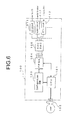
- Fig. 6 is a circuit diagram illustrating an example of the controller of the optical amplifying apparatus.
- the controller 100 includes an LD circuit 111 for controlling a driving current of the pumping LD, a heater circuit 112 for controlling the temperature of an EDF heater, a PD circuit 113 receiving detected signals of the PDs, a configuration ROM (Read Only Memory) 103 holding programs input from a user interface 102 via a CPU 101, an FPGA 104 for controlling the LD circuit 111, the heater circuit 112 and the like, an AD converter/DA converter 105 for performing DA conversion on a signal from the FPGA 104 to output the signal to the LD circuit 111, the heater circuit 112 and the like and performing AD conversion on signals from the PD circuit 113 and the like to output the signals to the FPGA 104, and other circuits.
- LD circuit 111 for controlling a driving current of the pumping LD
- a heater circuit 112 for controlling the temperature of an EDF heater
- a PD circuit 113 receiving detected
- two FPGAs may be used in the controller of the optical amplifying apparatus, and when one of the FPGAs is being program-updated, the other is used to perform various operations including monitoring of photo diodes, LD driving current control and temperature control.
- the FPGA 104 is prevented from performing various operations, which may causes such a problem that control of an optical signal propagating in the optical amplifying apparatus is interrupted, resulting in communication failure.
- various parameters in the FPGA 104 are erased they are required to be rewritten after updating, which takes a lot of time and effort.
- control of the optical amplifying apparatus is not interrupted.
- this configuration needs to be large-sized and expensive.
- the present invention has an object to provide an optical amplifying apparatus which allows simultaneous performance of optical amplification control and FPGA updating without any additional FPGA.
- a second aspect of the present invention is an optical amplifying apparatus of the first aspect, in which the devices comprise at least an optically pumping laser diode and the circuits comprise a laser diode circuit for setting a driving current of the laser diode.
- a fourth aspect of the present invention is an optical amplifying apparatus of the third aspect, in which, after a dither signal output from the gate array is turned off, the gate array measures the driving current the predetermined number of times successively to calculate out the average value.
- a fifth aspect of the present invention is an optical amplifying apparatus of any one of the first to fourth aspects, in which the devices comprise a monitoring element for monitoring an optical signal propagating in an optical fiber, and a detected signal from the monitoring element is sent to the CPU via an analog/digital converter.
- a gate array as firmware when a gate array as firmware is updated, device control to be performed by the gate array is performed instead by a latch unit and various parameters stored in the gate array are temporarily stored in another storing unit for backup.
- This configuration allows normal control of optical amplification even while the single gate array is being updated and easy reproduction of the various parameters that are deleted from the gate array during the updating.
- an optical amplifier 3 including an erbium-doped optical fiber (EDF) 1 connected to an optical transmission path and a first optical coupler 2 connected to the EDF1; a pumping laser diode (LD) 4 emitting optically pumping energy to the EDF 1 via the first optical coupler 2; a first photo diode (PD) 6 receiving via a second optical coupler 5 an optical signal which is to be input to the EDF 1 and performing photo-electric conversion on the optical signal; a second photo diode (PD) 8 receiving via a third optical coupler 7 an optical signal outputted from the optical amplifier 3 and performing photo-electric conversion on the optical signal; a heater 9 controlling the temperature of the EDF 1; and a controller 10 receiving electric signals from the first photo diode 6 and the second photo diode 8 and controlling based on these electric signals a driving current of the pumping LD 4 and the temperature of the heater 9.
- EDF erbium-doped optical fiber
- LD pumping laser diode
- PD photo diode
- the controller 10 has:, as illustrated in Fig. 2 , a CPU 11 for performing processing such as inputting and outputting of data between devices and controlling of the operation of each device; an FPGA 12 for rewritably storing a program for controlling the pumping LD 4 and the heater 9 and the like and storing various types of data and various parameters; a latch IC 13 for selectively outputting, based on an instruction from the CPU 11, a control signal, which is output from the FPGA 12 in a predetermined operation mode, as it is or an ACC (Auto Current Control) mode control signal based on preset data; a flash ROM 14 for storing programs and data; a user interface 15 for externally acting to store programs in the flash ROM 14 via the CPU 11; a SRAM (Static Random Access Memory) 16 for temporarily storing data of various parameters, which is stored in the FPGA 12, by processing of the CPU 11; an LD circuit 17 for setting the driving current of the pumping LD 4; a heater circuit 18 for setting a heating temperature of the heater;
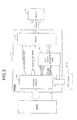
- the FPGA 12 includes, as illustrated in Fig. 3 , a shared memory 12a, an AGC calculation block 12b and a selector 12c.
- the shared memory 12a is configured to store various parameters and data including a parameter to be output to the LD circuit 17 for making a driving current and a dither signal pass to the pumping LD 4, a parameter to be output to the heater circuit 18 for controlling the temperature of the heater 9, a parameter to be output to the output interface 22 for external display, signals for selecting the control mode between the ACC mode and the AGC (Auto Gain Control) mode, control target values and detected values of the PDs 6 and 8 received from the PD circuit 19 via the AD converter 21 and also to output a signal for setting a control mode in response to a signal from the CPU 11 and ACC and AGC target values.
- AGC Automatic Gain Control
- the AGC calculation block 12b is configured to calculate parameters for AGC so as to control optical amplification in the AGC mode based on a control signal from the CPU 11 until program data is sent from the user interface 15 to the flash ROM 14.
- the AGC calculation block 12b calculates various parameters including a driving current of the pumping LD 4 based on the detected values of the PDs 6 and 8 received from the PD circuit 19 via the AD converter 21 in such a manner as to attain a gain target value of input/output power with an optical signal, then, outputs the calculated AGC parameters to the shared memory 12a and sends AGC target values obtained based on the calculation result to the selector 12c.
- the selector 12c is configured to selectively output ACC target values or AGC target values to the latch IC 13 based on a control mode setting signal from the shared memory 12a.
- the ACC target values include a parameter for controlling a driving current, dither signal and the like to keep optical power output from the pumping laser diode 4 constant.
- the LD circuit 17 Upon receiving the target values, the LD circuit 17 outputs a driving current and a dither signal to the pumping LD 4 while the heater circuit 18 outputs a control signal to control the temperature of the heater 9. Besides, the output interface 22 outputs a signal for controlling a display unit.
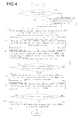
- the CPU 11 in the controller 10 stores the program output from the user interface 15 in the flash ROM 14 and controls the FPGA 12 in accordance with the flowchart shown in Fig. 4 .
- Fig. 4 first it is determined in the AGC mode control by the FPGA 12 whether the pumping LD 4 is controlled by a dither signal or not (S1 in Fig. 4 ).
- a dither signal When control by a dither signal is performed, amplitude and a frequency of the dither signal are set to "0" (S2 in Fig. 4 ).
- a target value of the driving current of the pumping LD 4 calculated by the AGC calculation block 12b is read by the shared memory 12a repeatedly, for example, 512 times, and the target values obtained by repeated calculation are used to obtain an average value thereof.
- This average value is then set as a target value of the driving current of the pumping LD 4 in the ACC mode operation (S3 in Fig. 4 ).
- the shared memory 12a is used to read the target value of the driving current continuously plural times, the dither signal is set to be invalid and therefore, the calculated target value hardly varies depending on measurement timing.
- the various parameters for AGC calculated and stored in the shared memory 12a and all other parameters are stored in the SRAM 16 for backup by the CPU 11 (S4 in Fig. 4 ).
- the CPU 11 sending a mode switching signal to the FPGA 12 and thereby, the control mode output from the shared memory 12a to the selector 12c is switched from the AGC mode to the ACC mode, and target values of the ACC mode including an average target value of the driving current of the pumping LD 4 obtained while disabling the dither signal are sent to the selector 12c (S5 in Fig. 4 ).
- the selector 12c outputs the ACC target signals to the LD circuit 17 and the like via the latch IC 13 and has the ACC target signals and their parameters stored in the latch IC 13.
- the CPU 11 confirms that the control mode of the shared memory 12a of the FPGA 12 becomes the ACC mode (S6 in Fig. 4 ). Later, the CPU 11 sends a control signal to the latch IC 13 and blocks control signals and data from the FPGA 12 to the latch IC 13. On the other hand, the ACC mode control signals and parameters stored in the latch IC 13 are continuously sent via the DA converter 20 to the LD circuit 17, the heater circuit 18 and the like, and control signals are also sent to the output interface 22 (S7 in Fig. 4 ).
- the CPU 11 erases the program and data in the FPGA 12 and writes in the FPGA 12 program data stored in the flash ROM 14 to update the FPGA program. Then, various parameters and other data saved in the SRAM are written again in the shared memory 12a of the FPGA 12 (S8 in Fig. 4 ). At this time, a parameter regarding the dither signal is also read from the SRAM 16 and written again in the shared memory 12a thereby to enable control by way of dither signals again.
- the latch IC 13 controls the pumping LD 4, the heater 9 and the like, control to the optical amplifying apparatus is kept on during program updating of the FPGA 12.
- detected values of the photo diodes 6 and 8 are also input to the CPU 11 via the PD circuit 19 and the AD converter 21, for example, such processing may be possible that the CPU 11 stops optical amplification when a detected signal of the first PD connected to the input side of the EDF1 is zero.
- the CPU 11 checks to see if the FPGA 12 operates normally (S9 in Fig. 4 )
- the CPU 11 controls the FPGA 12 to change the control mode set at the selector 12c by the shared memory 12a from the ACC mode to the AGC mode and to calculate various parameters for AGC mode by way of the AGC calculation block 12b to make the selector 12a output an AGC signal and AGC target values to the latch IC 13. Then, block state from the FPGA 12 to the latch IC 13 is released by the CPU 11 while the AGC mode control signal and target values controlled by the FPGA 12 are made to pass through the latch IC 13 to be output to the DA converter 20 and the output interface 22 (S10 in Fig. 4 ). Thus, the pumping LD 4 and the heater 9 are controlled by the various parameters of the AGC mode.
- Fig. 5 (a) is a graph of the case where the driving current target value of the pumping LD 4 was not averaged, showing fluctuation of an optical output from the EDF1 between the time when the pumping LD 4 was controlled by the latch IC 13 and the time when the pumping LD 4 was controlled by the FPGA 12.
- Fig. 5 (b) is a graph of the case where the driving current target value of the pumping LD 4 was averaged, showing no fluctuation of an optical output from the EDF1 occurring between the time when the pumping LD 4 was controlled by the latch IC 13 and the time when the pumping LD 4 was controlled by the FPGA 12.
Landscapes
- Physics & Mathematics (AREA)
- Electromagnetism (AREA)
- Engineering & Computer Science (AREA)
- Computer Networks & Wireless Communication (AREA)
- Signal Processing (AREA)
- Plasma & Fusion (AREA)
- Optics & Photonics (AREA)
- Optical Communication System (AREA)
- Lasers (AREA)
Abstract
Description
- The present invention relates to an optical amplifying apparatus and, more particularly, to an optical amplifying apparatus having a controller using an FPGA (FIELD PROGRAMMABLE GATE ARRAY) .
- The WDM (Wavelength Division Multiplexing) system is a system in which plural optical signals of different wavelengths are multiplexed into one optical transmission path. This WDM system adopts a configuration using an optical amplifying apparatus which is provided in an optical transmission path to control power of an optical signal and output the optical signal to the optical transmission path such as a single mode optical fiber (SMF) or a dispersion-shifted optical fiber (DSF).
- The optical amplifying apparatus includes an EDF (Erbium Doped Fiber) connected to some midpoint of an optical transmission path, a pumping LD (Laser Diode) for optically pumping the EDF, two PDs (Photo Diodes) for monitoring light input to or output from the EDF and a controller for controlling a driving current of the pumping LD based on outputs from the two PDs.
-
Fig. 6 is a circuit diagram illustrating an example of the controller of the optical amplifying apparatus. Thecontroller 100 includes anLD circuit 111 for controlling a driving current of the pumping LD, a heater circuit 112 for controlling the temperature of an EDF heater, aPD circuit 113 receiving detected signals of the PDs, a configuration ROM (Read Only Memory) 103 holding programs input from auser interface 102 via a CPU 101, anFPGA 104 for controlling theLD circuit 111, the heater circuit 112 and the like, an AD converter/DA converter 105 for performing DA conversion on a signal from theFPGA 104 to output the signal to theLD circuit 111, the heater circuit 112 and the like and performing AD conversion on signals from thePD circuit 113 and the like to output the signals to theFPGA 104, and other circuits. - In such a controller, the CPU 101 and
FPGA 104, which are firmware, can be updated or improved in function/performance by rewriting their programs.
In updating of theFPGA 104, theconfiguration ROM 103 receives data of a program and the like from theuser interface 102 and stores the data therein. Then, in response to an update request from the CPU 101, theFPGA 104 has the program rewritten with use of the data stored in theconfiguration ROM 103. This program rewriting takes about one second, for example. When the program is rewritten, various parameters in theFPGA 104 are reset. That is, the various parameters are also updated via the CPU 101. - FPGA program writing using a configuration element is disclosed, for example, in the following
non-patent document 1.
While theFPGA 104 is being updated, theFPGA 104 can not perform various controls of LD driving current and temperature via theLD circuit 111 and the heater circuit 112. - Meanwhile, the following
patent document 1 discloses use of two programmable controllers for machine control, of which one controls the machine performance and the other is in the backup mode, and when the one programmable controller is in trouble, the other takes over the control of the machine performance. - Here, with reference to the configuration disclosed in the
patent document 1, two FPGAs may be used in the controller of the optical amplifying apparatus, and when one of the FPGAs is being program-updated, the other is used to perform various operations including monitoring of photo diodes, LD driving current control and temperature control. - NON-patent document 1: Cyclone Device Handbook, Volumel, p.13-9, Altera Corporation, August 2005
- Patent document 1:
Japanese Patent Laid-open Publication No. 6(1994)-51802 - In the configuration illustrated in
Fig. 6 , if theFPGA 104 is updated during operation of the optical amplifying apparatus, theFPGA 104 is prevented from performing various operations, which may causes such a problem that control of an optical signal propagating in the optical amplifying apparatus is interrupted, resulting in communication failure. In addition, as various parameters in theFPGA 104 are erased they are required to be rewritten after updating, which takes a lot of time and effort.
On the other hand, if two FPGAs are used in the optical amplifying apparatus as disclosed in thepatent document 1, control of the optical amplifying apparatus is not interrupted. However, this configuration needs to be large-sized and expensive. - The present invention has an object to provide an optical amplifying apparatus which allows simultaneous performance of optical amplification control and FPGA updating without any additional FPGA.
- In order to solve the above-mentioned problems, a first aspect of the present invention is an optical amplifying apparatus comprising: a CPU for processing various signals; a plurality of circuits for controlling respective devices required for optical amplification; a first storing unit for storing a program supplied from a user; a gate array for storing various parameters for controlling the devices, the gate array being updated based on the program which is stored in the first storing unit and sent via the CPU; a latch unit, provided between the gate array and the circuits, for interrupting a signal path from the gate array to the circuits after receiving a starting signal of an update from the CPU until the update being finished and for controlling the circuits based on the parameters stored in the gate array before the signal path is interrupted; and a second storing unit for, at least during the update, storing the various parameters which are stored in the gate array before the update.
- A second aspect of the present invention is an optical amplifying apparatus of the first aspect, in which the devices comprise at least an optically pumping laser diode and the circuits comprise a laser diode circuit for setting a driving current of the laser diode.
- A third aspect of the present invention is an optical amplifying apparatus of the second aspect, in which the latch unit is configured to obtain an average value of the driving current of the laser diode which is calculated out by measuring the driving current of the laser diode a predetermined number of times successively before the update is started and to drive the laser diode with the average value during the update.
- A fourth aspect of the present invention is an optical amplifying apparatus of the third aspect, in which, after a dither signal output from the gate array is turned off, the gate array measures the driving current the predetermined number of times successively to calculate out the average value.
- A fifth aspect of the present invention is an optical amplifying apparatus of any one of the first to fourth aspects, in which the devices comprise a monitoring element for monitoring an optical signal propagating in an optical fiber, and a detected signal from the monitoring element is sent to the CPU via an analog/digital converter.
- According to the present invention, when a gate array as firmware is updated, device control to be performed by the gate array is performed instead by a latch unit and various parameters stored in the gate array are temporarily stored in another storing unit for backup. This configuration allows normal control of optical amplification even while the single gate array is being updated and easy reproduction of the various parameters that are deleted from the gate array during the updating.
-
-
Fig. 1 is a view illustrating a configuration of an optical amplifying apparatus according to one embodiment of the present invention; -
Fig. 2 is a block diagram illustrating a controller of the optical amplifying apparatus according to the embodiment of the present invention; -
Fig. 3 is a block diagram of an FPGA of the controller of the optical amplifying apparatus according to the embodiment of the present invention; -
Fig. 4 is a flow chart showing control performed during update of the FPGA of the controller of the optical amplifying apparatus according to the embodiment of the present invention; -
Figs. 5 (a) and 5 (b) are wave form charts showing outputs from the optical amplifying apparatus, one is of the case where an LD current target value is not averaged before the FPGA of the controller of the optical amplifying apparatus according to the embodiment of the present invention is updated, and the other is of the case when the LD current target value is averaged; and -
Fig. 6 is a block diagram illustrating a controller of an optical amplifying apparatus according to a conventional art. -
- 1:
- EDF
- 2, 5, 7:
- optical coupler
- 3:
- amplifier
- 4:
- pumping laser diode (LD)
- 9:
- heater
- 10:
- controller
- 11:
- CPU
- 12:
- FPGA
- 12a:
- shared memory
- 12b:
- AGC (Auto Gain Control) calculation block
- 12c:
- selector
- 13:
- latch IC
- 14:
- flash ROM
- 15:
- user interface
- 16:
- SRAM
- 17:
- LD circuit
- 18:
- heater circuit
- 19:
- PD circuit
- 20:
- DA converter
- 21:
- AD converter
- With reference to the drawings, an embodiment of the present invention will be described in detail below.
Fig. 1 is a view illustrating a configuration of an optical amplifying apparatus according to the embodiment of the present invention.
The optical amplifying apparatus according to the embodiment of the present invention includes: as illustrated inFig. 1 , anoptical amplifier 3 including an erbium-doped optical fiber (EDF) 1 connected to an optical transmission path and a firstoptical coupler 2 connected to the EDF1; a pumping laser diode (LD) 4 emitting optically pumping energy to theEDF 1 via the firstoptical coupler 2; a first photo diode (PD) 6 receiving via a secondoptical coupler 5 an optical signal which is to be input to theEDF 1 and performing photo-electric conversion on the optical signal; a second photo diode (PD) 8 receiving via a thirdoptical coupler 7 an optical signal outputted from theoptical amplifier 3 and performing photo-electric conversion on the optical signal; aheater 9 controlling the temperature of theEDF 1; and acontroller 10 receiving electric signals from thefirst photo diode 6 and thesecond photo diode 8 and controlling based on these electric signals a driving current of thepumping LD 4 and the temperature of theheater 9. - The controller 10 has:, as illustrated in
Fig. 2 , a CPU 11 for performing processing such as inputting and outputting of data between devices and controlling of the operation of each device; an FPGA 12 for rewritably storing a program for controlling the pumping LD 4 and the heater 9 and the like and storing various types of data and various parameters; a latch IC 13 for selectively outputting, based on an instruction from the CPU 11, a control signal, which is output from the FPGA 12 in a predetermined operation mode, as it is or an ACC (Auto Current Control) mode control signal based on preset data; a flash ROM 14 for storing programs and data; a user interface 15 for externally acting to store programs in the flash ROM 14 via the CPU 11; a SRAM (Static Random Access Memory) 16 for temporarily storing data of various parameters, which is stored in the FPGA 12, by processing of the CPU 11; an LD circuit 17 for setting the driving current of the pumping LD 4; a heater circuit 18 for setting a heating temperature of the heater; a PD circuit 19 for receiving signals outputted from the PDs 6 and 8; a DA converter 20 for converting a digital signal output from the latch IC 13 to an analog signal to output the signal to the LD circuit 17 and the heater circuit 18; an AD converter 21 for converting an analog signal output from the PD circuit 19 to a digital signal to output the signal to the FPGA 12 and CPU 11; an output interface 22 relaying display signals output from the latch IC 13; and the like. - The
FPGA 12 includes, as illustrated inFig. 3 , a sharedmemory 12a, anAGC calculation block 12b and aselector 12c.
The sharedmemory 12a is configured to store various parameters and data including a parameter to be output to theLD circuit 17 for making a driving current and a dither signal pass to thepumping LD 4, a parameter to be output to the heater circuit 18 for controlling the temperature of theheater 9, a parameter to be output to the output interface 22 for external display, signals for selecting the control mode between the ACC mode and the AGC (Auto Gain Control) mode, control target values and detected values of thePDs PD circuit 19 via theAD converter 21 and also to output a signal for setting a control mode in response to a signal from theCPU 11 and ACC and AGC target values. - Besides, the
AGC calculation block 12b is configured to calculate parameters for AGC so as to control optical amplification in the AGC mode based on a control signal from theCPU 11 until program data is sent from theuser interface 15 to theflash ROM 14. For example, theAGC calculation block 12b calculates various parameters including a driving current of thepumping LD 4 based on the detected values of thePDs PD circuit 19 via theAD converter 21 in such a manner as to attain a gain target value of input/output power with an optical signal, then, outputs the calculated AGC parameters to the sharedmemory 12a and sends AGC target values obtained based on the calculation result to theselector 12c. - The
selector 12c is configured to selectively output ACC target values or AGC target values to thelatch IC 13 based on a control mode setting signal from the sharedmemory 12a. Here, the ACC target values include a parameter for controlling a driving current, dither signal and the like to keep optical power output from the pumpinglaser diode 4 constant.
Next description is made about updating of anFPGA 12 program in the above-mentionedcontroller 10 of the optical amplifying apparatus. - First, the
controller 10 operates in the AGC mode in accordance with a pre-update program. That is, in theFPGA 12 illustrated inFig. 3 , the sharedmemory 12a sends theselector 12c a signal for setting the AGC mode as control mode, and AGC target values sent from the sharedmemory 12a are selected to control theLD circuit 17, the heater circuit 18 and the like via thelatch IC 13 in such a manner as to obtain a predetermined gain in the AGC mode. - The AGC target values are calculated out by the
AGC calculation block 12b based on detected values of thefirst PD 6 and thesecond PD 8 received from theAD converter 21 and the various parameters so as to have a target value of gain. The thus-obtained target values of the parameters are output from theselector 12c to thelatch IC 13. In this case, upon receiving the target values from theFPGA 12, thelatch IC 13 then outputs the target values as they are to the output interface 22 or outputs to theLD circuit 17 and the heater circuit 18 via theDA converter 20. - Upon receiving the target values, the
LD circuit 17 outputs a driving current and a dither signal to thepumping LD 4 while the heater circuit 18 outputs a control signal to control the temperature of theheater 9. Besides, the output interface 22 outputs a signal for controlling a display unit.
During such AGC mode operation, when an updated program is output from theuser interface 15 to thecontroller 10, theCPU 11 in thecontroller 10 stores the program output from theuser interface 15 in theflash ROM 14 and controls theFPGA 12 in accordance with the flowchart shown inFig. 4 . - In
Fig. 4 , first it is determined in the AGC mode control by theFPGA 12 whether thepumping LD 4 is controlled by a dither signal or not (S1 inFig. 4 ). When control by a dither signal is performed, amplitude and a frequency of the dither signal are set to "0" (S2 inFig. 4 ).
Then, a target value of the driving current of thepumping LD 4 calculated by theAGC calculation block 12b is read by the sharedmemory 12a repeatedly, for example, 512 times, and the target values obtained by repeated calculation are used to obtain an average value thereof. This average value is then set as a target value of the driving current of thepumping LD 4 in the ACC mode operation (S3 inFig. 4 ). Here, when the sharedmemory 12a is used to read the target value of the driving current continuously plural times, the dither signal is set to be invalid and therefore, the calculated target value hardly varies depending on measurement timing. - Further, the various parameters for AGC calculated and stored in the shared
memory 12a and all other parameters are stored in theSRAM 16 for backup by the CPU 11 (S4 inFig. 4 ).
This is followed by theCPU 11 sending a mode switching signal to theFPGA 12 and thereby, the control mode output from the sharedmemory 12a to theselector 12c is switched from the AGC mode to the ACC mode, and target values of the ACC mode including an average target value of the driving current of thepumping LD 4 obtained while disabling the dither signal are sent to theselector 12c (S5 inFig. 4 ). Then, theselector 12c outputs the ACC target signals to theLD circuit 17 and the like via thelatch IC 13 and has the ACC target signals and their parameters stored in thelatch IC 13. - Then, the
CPU 11 confirms that the control mode of the sharedmemory 12a of theFPGA 12 becomes the ACC mode (S6 inFig. 4 ).
Later, theCPU 11 sends a control signal to thelatch IC 13 and blocks control signals and data from theFPGA 12 to thelatch IC 13. On the other hand, the ACC mode control signals and parameters stored in thelatch IC 13 are continuously sent via theDA converter 20 to theLD circuit 17, the heater circuit 18 and the like, and control signals are also sent to the output interface 22 (S7 inFig. 4 ). - After the ACC mode control held by the
latch IC 13 is started, theCPU 11 erases the program and data in theFPGA 12 and writes in theFPGA 12 program data stored in theflash ROM 14 to update the FPGA program. Then, various parameters and other data saved in the SRAM are written again in the sharedmemory 12a of the FPGA 12 (S8 inFig. 4 ). At this time, a parameter regarding the dither signal is also read from theSRAM 16 and written again in the sharedmemory 12a thereby to enable control by way of dither signals again. - Then, as the
latch IC 13 controls thepumping LD 4, theheater 9 and the like, control to the optical amplifying apparatus is kept on during program updating of theFPGA 12. Further, as detected values of thephoto diodes CPU 11 via thePD circuit 19 and theAD converter 21, for example, such processing may be possible that theCPU 11 stops optical amplification when a detected signal of the first PD connected to the input side of the EDF1 is zero.
After theFPGA 12 updating is finished and restarted, theCPU 11 checks to see if theFPGA 12 operates normally (S9 inFig. 4 ) - As AGC mode control becomes possible in this state, the
CPU 11 controls theFPGA 12 to change the control mode set at theselector 12c by the sharedmemory 12a from the ACC mode to the AGC mode and to calculate various parameters for AGC mode by way of theAGC calculation block 12b to make theselector 12a output an AGC signal and AGC target values to thelatch IC 13.
Then, block state from theFPGA 12 to thelatch IC 13 is released by theCPU 11 while the AGC mode control signal and target values controlled by theFPGA 12 are made to pass through thelatch IC 13 to be output to theDA converter 20 and the output interface 22 (S10 inFig. 4 ).
Thus, thepumping LD 4 and theheater 9 are controlled by the various parameters of the AGC mode. - Here, the operation of the optical amplifier was checked in the three phases of while the FPGA program was being updated following the above-described flow and before and after the program was updated. This check result reveals that optical input and output of the EDF1 were not changed nor interrupted which the FPGA program was updated and the optical amplification was continuously controlled.
- Meanwhile, comparison was made between the case where the driving current target value of the
pumping LD 4 was averaged before the program of theFPGA 12 was updated and the case where the driving current target value was not averaged, which is shown inFigs. 5(a) and 5(b) .
Fig. 5 (a) is a graph of the case where the driving current target value of thepumping LD 4 was not averaged, showing fluctuation of an optical output from the EDF1 between the time when thepumping LD 4 was controlled by thelatch IC 13 and the time when thepumping LD 4 was controlled by theFPGA 12. - On the other hand,
Fig. 5 (b) is a graph of the case where the driving current target value of thepumping LD 4 was averaged, showing no fluctuation of an optical output from the EDF1 occurring between the time when thepumping LD 4 was controlled by thelatch IC 13 and the time when thepumping LD 4 was controlled by theFPGA 12.
These results show that when the driving current of thepumping LD 4 is controlled by thelatch IC 13 in the ACC mode, it is necessary to first obtain an average value of the driving current of thepumping LD 4 controlled by theFPGA 12 in the AGC mode while no dither signal is disabled, and then, to use this average value as a driving current value in the ACC mode, thereby assuring stable optical amplification even during program updating of theFPGA 12.
Claims (5)
- An optical amplifying apparatus comprising:a CPU for processing various signals;a plurality of circuits for controlling respective devices required for optical amplification;a first storing unit for storing a program supplied from a user;a gate array for storing various parameters for controlling the devices, the gate array being updated based on the program which is stored in the first storing unit and sent via the CPU;a latch unit, provided between the gate array and the circuits, for interrupting a signal path from the gate array to the circuits after receiving a starting signal of an update from the CPU until the update being finished and for controlling the circuits based on the parameters stored in the gate array before the signal path is interrupted; anda second storing unit for, at least during the update, storing the various parameters which are stored in the gate array before the update.
- The optical amplifying apparatus of claim 1, wherein the devices comprise at least an optically pumping laser diode and the circuits comprise a laser diode circuit for setting a driving current of the laser diode.
- The optical amplifying apparatus of claim 2, wherein the latch unit is configured to obtain an average value of the driving current of the laser diode which is calculated out by measuring the driving current of the laser diode a predetermined number of times successively before the update is started and to drive the laser diode with the average value during the update.
- The optical amplifying apparatus of claim 3, wherein, after a dither signal output from the gate array is turned off, the gate array measures the driving current the predetermined number of times successively to calculate out the average value.
- The optical amplifying apparatus of any one of claims 1 to 4, wherein the devices comprise a monitoring element for monitoring an optical signal propagating in an optical fiber, and a detected signal from the monitoring element is sent to the CPU via an analog/digital converter.
Applications Claiming Priority (2)
| Application Number | Priority Date | Filing Date | Title |
|---|---|---|---|
| JP2006041146A JP4234720B2 (en) | 2006-02-17 | 2006-02-17 | Optical amplifier |
| PCT/JP2007/052764 WO2007094425A1 (en) | 2006-02-17 | 2007-02-15 | Light amplifying apparatus |
Publications (3)
| Publication Number | Publication Date |
|---|---|
| EP1892805A1 true EP1892805A1 (en) | 2008-02-27 |
| EP1892805A4 EP1892805A4 (en) | 2012-05-09 |
| EP1892805B1 EP1892805B1 (en) | 2017-10-04 |
Family
ID=38371602
Family Applications (1)
| Application Number | Title | Priority Date | Filing Date |
|---|---|---|---|
| EP07714294.1A Not-in-force EP1892805B1 (en) | 2006-02-17 | 2007-02-15 | Light amplifying apparatus |
Country Status (4)
| Country | Link |
|---|---|
| US (1) | US7852550B2 (en) |
| EP (1) | EP1892805B1 (en) |
| JP (1) | JP4234720B2 (en) |
| WO (1) | WO2007094425A1 (en) |
Families Citing this family (16)
| Publication number | Priority date | Publication date | Assignee | Title |
|---|---|---|---|---|
| JP4999109B2 (en) * | 2008-03-28 | 2012-08-15 | 古河電気工業株式会社 | Optical device control method and optical device control apparatus |
| JP5224361B2 (en) * | 2008-11-12 | 2013-07-03 | 古河電気工業株式会社 | Optical module and control method thereof |
| WO2010116476A1 (en) | 2009-03-30 | 2010-10-14 | 富士通オプティカルコンポーネンツ株式会社 | Optical device |
| EP2440016B1 (en) * | 2010-10-08 | 2019-01-23 | Lantiq Beteiligungs-GmbH & Co.KG | Laser diode control device |
| JP5845657B2 (en) * | 2011-06-28 | 2016-01-20 | 富士通株式会社 | Control device, optical receiver, and control method |
| JP2014082592A (en) * | 2012-10-15 | 2014-05-08 | Sumitomo Electric Ind Ltd | Optical module for optical communication system and method of updating firmware of optical module for optical communication system |
| US9078054B2 (en) * | 2012-10-15 | 2015-07-07 | Sumitomo Electric Industries, Ltd. | Optical module used in optical communication systems, method of updating firmware of optical module used in optical communication systems, and trouble tracing system |
| JP6020055B2 (en) | 2012-11-06 | 2016-11-02 | 富士通株式会社 | Transmission apparatus and transmission system |
| JP6003581B2 (en) | 2012-11-26 | 2016-10-05 | 富士通株式会社 | Optical amplifier |
| JPWO2014104355A1 (en) * | 2012-12-28 | 2017-01-19 | 古河電気工業株式会社 | Optical transmission system |
| JP6096022B2 (en) * | 2013-03-25 | 2017-03-15 | 株式会社フジクラ | Determination method of output light power drop and optical amplification system in fiber laser device |
| US9494484B2 (en) | 2014-03-09 | 2016-11-15 | Ii-Vi Incorporated | In-service optical time domain reflectometry utilizing raman pump source |
| US10263384B2 (en) * | 2016-10-14 | 2019-04-16 | Lumenis Ltd. | Laser system having a dual pulse-length regime |
| CN109687278B (en) | 2019-01-02 | 2021-05-11 | 武汉光迅科技股份有限公司 | A kind of method and device for online upgrade program of optical amplifier |
| JP7343324B2 (en) * | 2019-07-26 | 2023-09-12 | ファナック株式会社 | Control device and control method for controlling a laser oscillator |
| CN113050462B (en) * | 2019-12-26 | 2025-06-03 | 福州高意通讯有限公司 | Structure and control method for achieving uninterrupted EDFA optical output |
Family Cites Families (9)
| Publication number | Priority date | Publication date | Assignee | Title |
|---|---|---|---|---|
| US5313386A (en) * | 1992-06-11 | 1994-05-17 | Allen-Bradley Company, Inc. | Programmable controller with backup capability |
| JPH10240561A (en) * | 1997-02-27 | 1998-09-11 | Kokusai Electric Co Ltd | Emulator for FPGA boot and FPGA boot method |
| US6557101B1 (en) * | 1999-12-22 | 2003-04-29 | Sycamore Networks, Inc. | Methods and apparatus for upgrading programmable control logic without disturbing network traffic flowing through functional elements controlled by the control logic |
| US6631027B2 (en) * | 2000-04-13 | 2003-10-07 | Corning Incorporated | Universal controller for an optical amplifier that operates over a wide dynamic range of optical signals and optical amplifiers utilizing such controllers |
| JP2002305438A (en) * | 2001-04-05 | 2002-10-18 | Hitachi Ltd | FPGA, method of changing function of FPGA, and communication device using the same |
| JP2002314488A (en) * | 2001-04-12 | 2002-10-25 | Mitsubishi Electric Corp | Optical amplifier and optical amplification method |
| US6687049B1 (en) * | 2001-07-03 | 2004-02-03 | Onetta, Inc. | Optical amplifiers with stable output power under low input power conditions |
| KR100416975B1 (en) * | 2001-07-10 | 2004-02-05 | 삼성전자주식회사 | Auto gain control device of a fiber amplifier |
| AU2003244982A1 (en) * | 2002-07-04 | 2004-01-23 | Koninklijke Philips Electronics N.V. | Optical signal receiving unit and apparatus for reproducing information |
-
2006
- 2006-02-17 JP JP2006041146A patent/JP4234720B2/en not_active Expired - Fee Related
-
2007
- 2007-02-15 EP EP07714294.1A patent/EP1892805B1/en not_active Not-in-force
- 2007-02-15 WO PCT/JP2007/052764 patent/WO2007094425A1/en not_active Ceased
-
2008
- 2008-01-15 US US12/014,514 patent/US7852550B2/en active Active
Also Published As
| Publication number | Publication date |
|---|---|
| WO2007094425A1 (en) | 2007-08-23 |
| JP4234720B2 (en) | 2009-03-04 |
| EP1892805B1 (en) | 2017-10-04 |
| US7852550B2 (en) | 2010-12-14 |
| EP1892805A4 (en) | 2012-05-09 |
| JP2007220977A (en) | 2007-08-30 |
| US20080205460A1 (en) | 2008-08-28 |
Similar Documents
| Publication | Publication Date | Title |
|---|---|---|
| US7852550B2 (en) | Optical amplifying apparatus | |
| EP1283567B1 (en) | Automatic gain control device of optical fiber amplifier | |
| US8446923B2 (en) | Fiber laser device | |
| JP5098807B2 (en) | Optical signal adjustment method and optical signal adjustment device | |
| JP2723067B2 (en) | Optical amplifier | |
| JPH06209290A (en) | Optical subsystem | |
| US10965375B2 (en) | Optical node device | |
| US20110081146A1 (en) | Optical monitor device | |
| GB2328574A (en) | Dual feedback loop power control in an optical fibre amplifier | |
| JP2000277842A (en) | Optical component, optical amplifier, and method for controlling characteristics of optical amplifier | |
| US20190148904A1 (en) | Method of controlling optical transmitter, and optical transmitter | |
| JP4941017B2 (en) | OPTICAL AMPLIFIER, ITS CONTROL DEVICE, CONTROL CIRCUIT, CONTROL METHOD, CONTROL PROGRAM, AND OPTICAL COMMUNICATION NETWORK | |
| US20090154506A1 (en) | Tunable laser module | |
| US6900929B2 (en) | Noise figure measuring system for optical amplifier | |
| JP3449171B2 (en) | Optical amplifier | |
| EP1460782B1 (en) | Optical amplifier | |
| US20240348000A1 (en) | Optical amplification system, optical amplification method, and storage medium | |
| JPH08265259A (en) | Optical amplification repeater | |
| JP7073895B2 (en) | Optical transmitter and control method of optical transmitter | |
| JP2002084024A (en) | Optical amplifier | |
| KR101616980B1 (en) | apparatus of generating wavelength tunable laser | |
| JP2795544B2 (en) | Fiber type optical amplifier | |
| JP2001160651A (en) | Semiconductor laser output control device and optical signal transmission system | |
| JP2002314488A (en) | Optical amplifier and optical amplification method | |
| JP4768252B2 (en) | Optical amplifier and optical output adjustment method |
Legal Events
| Date | Code | Title | Description |
|---|---|---|---|
| PUAI | Public reference made under article 153(3) epc to a published international application that has entered the european phase |
Free format text: ORIGINAL CODE: 0009012 |
|
| 17P | Request for examination filed |
Effective date: 20071120 |
|
| AK | Designated contracting states |
Kind code of ref document: A1 Designated state(s): AT BE BG CH CY CZ DE DK EE ES FI FR GB GR HU IE IS IT LI LT LU LV MC NL PL PT RO SE SI SK TR |
|
| AX | Request for extension of the european patent |
Extension state: AL BA HR MK YU |
|
| DAX | Request for extension of the european patent (deleted) | ||
| A4 | Supplementary search report drawn up and despatched |
Effective date: 20120411 |
|
| RIC1 | Information provided on ipc code assigned before grant |
Ipc: H01S 3/10 20060101AFI20120403BHEP Ipc: H01S 3/06 20060101ALI20120403BHEP Ipc: H04B 10/16 20060101ALI20120403BHEP Ipc: H04B 10/17 20060101ALI20120403BHEP |
|
| DAX | Request for extension of the european patent (deleted) | ||
| 17Q | First examination report despatched |
Effective date: 20141117 |
|
| RIC1 | Information provided on ipc code assigned before grant |
Ipc: H04B 10/294 20130101ALI20170322BHEP Ipc: H01S 3/06 20060101ALI20170322BHEP Ipc: H01S 3/10 20060101AFI20170322BHEP |
|
| GRAP | Despatch of communication of intention to grant a patent |
Free format text: ORIGINAL CODE: EPIDOSNIGR1 |
|
| STAA | Information on the status of an ep patent application or granted ep patent |
Free format text: STATUS: GRANT OF PATENT IS INTENDED |
|
| INTG | Intention to grant announced |
Effective date: 20170515 |
|
| RIN1 | Information on inventor provided before grant (corrected) |
Inventor name: YOSHIKAWA, TORU Inventor name: OKANIWA, TAKEO Inventor name: WU, JIE Inventor name: KAGI, NOBUYUKI |
|
| GRAS | Grant fee paid |
Free format text: ORIGINAL CODE: EPIDOSNIGR3 |
|
| GRAJ | Information related to disapproval of communication of intention to grant by the applicant or resumption of examination proceedings by the epo deleted |
Free format text: ORIGINAL CODE: EPIDOSDIGR1 |
|
| GRAL | Information related to payment of fee for publishing/printing deleted |
Free format text: ORIGINAL CODE: EPIDOSDIGR3 |
|
| STAA | Information on the status of an ep patent application or granted ep patent |
Free format text: STATUS: EXAMINATION IS IN PROGRESS |
|
| GRAA | (expected) grant |
Free format text: ORIGINAL CODE: 0009210 |
|
| GRAR | Information related to intention to grant a patent recorded |
Free format text: ORIGINAL CODE: EPIDOSNIGR71 |
|
| STAA | Information on the status of an ep patent application or granted ep patent |
Free format text: STATUS: THE PATENT HAS BEEN GRANTED |
|
| INTC | Intention to grant announced (deleted) | ||
| AK | Designated contracting states |
Kind code of ref document: B1 Designated state(s): AT BE BG CH CY CZ DE DK EE ES FI FR GB GR HU IE IS IT LI LT LU LV MC NL PL PT RO SE SI SK TR |
|
| INTG | Intention to grant announced |
Effective date: 20170830 |
|
| REG | Reference to a national code |
Ref country code: GB Ref legal event code: FG4D |
|
| REG | Reference to a national code |
Ref country code: CH Ref legal event code: EP |
|
| REG | Reference to a national code |
Ref country code: AT Ref legal event code: REF Ref document number: 934842 Country of ref document: AT Kind code of ref document: T Effective date: 20171015 |
|
| REG | Reference to a national code |
Ref country code: IE Ref legal event code: FG4D |
|
| REG | Reference to a national code |
Ref country code: DE Ref legal event code: R096 Ref document number: 602007052561 Country of ref document: DE |
|
| REG | Reference to a national code |
Ref country code: NL Ref legal event code: MP Effective date: 20171004 |
|
| REG | Reference to a national code |
Ref country code: LT Ref legal event code: MG4D |
|
| REG | Reference to a national code |
Ref country code: AT Ref legal event code: MK05 Ref document number: 934842 Country of ref document: AT Kind code of ref document: T Effective date: 20171004 |
|
| PG25 | Lapsed in a contracting state [announced via postgrant information from national office to epo] |
Ref country code: NL Free format text: LAPSE BECAUSE OF FAILURE TO SUBMIT A TRANSLATION OF THE DESCRIPTION OR TO PAY THE FEE WITHIN THE PRESCRIBED TIME-LIMIT Effective date: 20171004 |
|
| PG25 | Lapsed in a contracting state [announced via postgrant information from national office to epo] |
Ref country code: FI Free format text: LAPSE BECAUSE OF FAILURE TO SUBMIT A TRANSLATION OF THE DESCRIPTION OR TO PAY THE FEE WITHIN THE PRESCRIBED TIME-LIMIT Effective date: 20171004 Ref country code: LT Free format text: LAPSE BECAUSE OF FAILURE TO SUBMIT A TRANSLATION OF THE DESCRIPTION OR TO PAY THE FEE WITHIN THE PRESCRIBED TIME-LIMIT Effective date: 20171004 Ref country code: ES Free format text: LAPSE BECAUSE OF FAILURE TO SUBMIT A TRANSLATION OF THE DESCRIPTION OR TO PAY THE FEE WITHIN THE PRESCRIBED TIME-LIMIT Effective date: 20171004 Ref country code: SE Free format text: LAPSE BECAUSE OF FAILURE TO SUBMIT A TRANSLATION OF THE DESCRIPTION OR TO PAY THE FEE WITHIN THE PRESCRIBED TIME-LIMIT Effective date: 20171004 |
|
| PG25 | Lapsed in a contracting state [announced via postgrant information from national office to epo] |
Ref country code: LV Free format text: LAPSE BECAUSE OF FAILURE TO SUBMIT A TRANSLATION OF THE DESCRIPTION OR TO PAY THE FEE WITHIN THE PRESCRIBED TIME-LIMIT Effective date: 20171004 Ref country code: BG Free format text: LAPSE BECAUSE OF FAILURE TO SUBMIT A TRANSLATION OF THE DESCRIPTION OR TO PAY THE FEE WITHIN THE PRESCRIBED TIME-LIMIT Effective date: 20180104 Ref country code: AT Free format text: LAPSE BECAUSE OF FAILURE TO SUBMIT A TRANSLATION OF THE DESCRIPTION OR TO PAY THE FEE WITHIN THE PRESCRIBED TIME-LIMIT Effective date: 20171004 Ref country code: GR Free format text: LAPSE BECAUSE OF FAILURE TO SUBMIT A TRANSLATION OF THE DESCRIPTION OR TO PAY THE FEE WITHIN THE PRESCRIBED TIME-LIMIT Effective date: 20180105 Ref country code: IS Free format text: LAPSE BECAUSE OF FAILURE TO SUBMIT A TRANSLATION OF THE DESCRIPTION OR TO PAY THE FEE WITHIN THE PRESCRIBED TIME-LIMIT Effective date: 20180204 |
|
| REG | Reference to a national code |
Ref country code: DE Ref legal event code: R097 Ref document number: 602007052561 Country of ref document: DE |
|
| PG25 | Lapsed in a contracting state [announced via postgrant information from national office to epo] |
Ref country code: SK Free format text: LAPSE BECAUSE OF FAILURE TO SUBMIT A TRANSLATION OF THE DESCRIPTION OR TO PAY THE FEE WITHIN THE PRESCRIBED TIME-LIMIT Effective date: 20171004 Ref country code: DK Free format text: LAPSE BECAUSE OF FAILURE TO SUBMIT A TRANSLATION OF THE DESCRIPTION OR TO PAY THE FEE WITHIN THE PRESCRIBED TIME-LIMIT Effective date: 20171004 Ref country code: CZ Free format text: LAPSE BECAUSE OF FAILURE TO SUBMIT A TRANSLATION OF THE DESCRIPTION OR TO PAY THE FEE WITHIN THE PRESCRIBED TIME-LIMIT Effective date: 20171004 Ref country code: EE Free format text: LAPSE BECAUSE OF FAILURE TO SUBMIT A TRANSLATION OF THE DESCRIPTION OR TO PAY THE FEE WITHIN THE PRESCRIBED TIME-LIMIT Effective date: 20171004 |
|
| PLBE | No opposition filed within time limit |
Free format text: ORIGINAL CODE: 0009261 |
|
| STAA | Information on the status of an ep patent application or granted ep patent |
Free format text: STATUS: NO OPPOSITION FILED WITHIN TIME LIMIT |
|
| PG25 | Lapsed in a contracting state [announced via postgrant information from national office to epo] |
Ref country code: PL Free format text: LAPSE BECAUSE OF FAILURE TO SUBMIT A TRANSLATION OF THE DESCRIPTION OR TO PAY THE FEE WITHIN THE PRESCRIBED TIME-LIMIT Effective date: 20171004 Ref country code: RO Free format text: LAPSE BECAUSE OF FAILURE TO SUBMIT A TRANSLATION OF THE DESCRIPTION OR TO PAY THE FEE WITHIN THE PRESCRIBED TIME-LIMIT Effective date: 20171004 |
|
| REG | Reference to a national code |
Ref country code: DE Ref legal event code: R119 Ref document number: 602007052561 Country of ref document: DE |
|
| 26N | No opposition filed |
Effective date: 20180705 |
|
| REG | Reference to a national code |
Ref country code: CH Ref legal event code: PL |
|
| PG25 | Lapsed in a contracting state [announced via postgrant information from national office to epo] |
Ref country code: MC Free format text: LAPSE BECAUSE OF FAILURE TO SUBMIT A TRANSLATION OF THE DESCRIPTION OR TO PAY THE FEE WITHIN THE PRESCRIBED TIME-LIMIT Effective date: 20171004 |
|
| GBPC | Gb: european patent ceased through non-payment of renewal fee |
Effective date: 20180215 |
|
| REG | Reference to a national code |
Ref country code: IE Ref legal event code: MM4A |
|
| REG | Reference to a national code |
Ref country code: BE Ref legal event code: MM Effective date: 20180228 |
|
| PG25 | Lapsed in a contracting state [announced via postgrant information from national office to epo] |
Ref country code: LU Free format text: LAPSE BECAUSE OF NON-PAYMENT OF DUE FEES Effective date: 20180215 Ref country code: SI Free format text: LAPSE BECAUSE OF FAILURE TO SUBMIT A TRANSLATION OF THE DESCRIPTION OR TO PAY THE FEE WITHIN THE PRESCRIBED TIME-LIMIT Effective date: 20171004 Ref country code: CH Free format text: LAPSE BECAUSE OF NON-PAYMENT OF DUE FEES Effective date: 20180228 Ref country code: LI Free format text: LAPSE BECAUSE OF NON-PAYMENT OF DUE FEES Effective date: 20180228 |
|
| REG | Reference to a national code |
Ref country code: FR Ref legal event code: ST Effective date: 20181031 |
|
| PG25 | Lapsed in a contracting state [announced via postgrant information from national office to epo] |
Ref country code: DE Free format text: LAPSE BECAUSE OF NON-PAYMENT OF DUE FEES Effective date: 20180901 Ref country code: IE Free format text: LAPSE BECAUSE OF NON-PAYMENT OF DUE FEES Effective date: 20180215 |
|
| PG25 | Lapsed in a contracting state [announced via postgrant information from national office to epo] |
Ref country code: GB Free format text: LAPSE BECAUSE OF NON-PAYMENT OF DUE FEES Effective date: 20180215 Ref country code: BE Free format text: LAPSE BECAUSE OF NON-PAYMENT OF DUE FEES Effective date: 20180228 Ref country code: FR Free format text: LAPSE BECAUSE OF NON-PAYMENT OF DUE FEES Effective date: 20180228 |
|
| PGFP | Annual fee paid to national office [announced via postgrant information from national office to epo] |
Ref country code: IT Payment date: 20190221 Year of fee payment: 13 |
|
| PG25 | Lapsed in a contracting state [announced via postgrant information from national office to epo] |
Ref country code: TR Free format text: LAPSE BECAUSE OF FAILURE TO SUBMIT A TRANSLATION OF THE DESCRIPTION OR TO PAY THE FEE WITHIN THE PRESCRIBED TIME-LIMIT Effective date: 20171004 |
|
| PG25 | Lapsed in a contracting state [announced via postgrant information from national office to epo] |
Ref country code: PT Free format text: LAPSE BECAUSE OF FAILURE TO SUBMIT A TRANSLATION OF THE DESCRIPTION OR TO PAY THE FEE WITHIN THE PRESCRIBED TIME-LIMIT Effective date: 20171004 Ref country code: HU Free format text: LAPSE BECAUSE OF FAILURE TO SUBMIT A TRANSLATION OF THE DESCRIPTION OR TO PAY THE FEE WITHIN THE PRESCRIBED TIME-LIMIT; INVALID AB INITIO Effective date: 20070215 |
|
| PG25 | Lapsed in a contracting state [announced via postgrant information from national office to epo] |
Ref country code: CY Free format text: LAPSE BECAUSE OF FAILURE TO SUBMIT A TRANSLATION OF THE DESCRIPTION OR TO PAY THE FEE WITHIN THE PRESCRIBED TIME-LIMIT Effective date: 20171004 |
|
| PG25 | Lapsed in a contracting state [announced via postgrant information from national office to epo] |
Ref country code: IT Free format text: LAPSE BECAUSE OF NON-PAYMENT OF DUE FEES Effective date: 20200215 |