EP1890526A1 - Handheld electronic device including multi-compartment shielding container and associated methods - Google Patents
Handheld electronic device including multi-compartment shielding container and associated methods Download PDFInfo
- Publication number
- EP1890526A1 EP1890526A1 EP06119181A EP06119181A EP1890526A1 EP 1890526 A1 EP1890526 A1 EP 1890526A1 EP 06119181 A EP06119181 A EP 06119181A EP 06119181 A EP06119181 A EP 06119181A EP 1890526 A1 EP1890526 A1 EP 1890526A1
- Authority
- EP
- European Patent Office
- Prior art keywords
- shielding
- base
- pair
- electronic device
- handheld electronic
- Prior art date
- Legal status (The legal status is an assumption and is not a legal conclusion. Google has not performed a legal analysis and makes no representation as to the accuracy of the status listed.)
- Granted
Links
Images




Classifications
-
- H—ELECTRICITY
- H05—ELECTRIC TECHNIQUES NOT OTHERWISE PROVIDED FOR
- H05K—PRINTED CIRCUITS; CASINGS OR CONSTRUCTIONAL DETAILS OF ELECTRIC APPARATUS; MANUFACTURE OF ASSEMBLAGES OF ELECTRICAL COMPONENTS
- H05K9/00—Screening of apparatus or components against electric or magnetic fields
- H05K9/0007—Casings
- H05K9/002—Casings with localised screening
- H05K9/0022—Casings with localised screening of components mounted on printed circuit boards [PCB]
- H05K9/0024—Shield cases mounted on a PCB, e.g. cans or caps or conformal shields
- H05K9/0032—Shield cases mounted on a PCB, e.g. cans or caps or conformal shields having multiple parts, e.g. frames mating with lids
Definitions
- the present invention relates to the field of mobile communications, and, more particularly, to shielding within a mobile communication device and related methods.
- PDA Personal Digital Assistant
- GSM Global System for Mobile communications
- interfering signals can be generated when the liquid crystal display (LCD) in some mobile wireless communications devices radiates radio frequency (RF) interfering energy and degrades receiver sensitivity. This may be problematic where the interfering energy is generated by the microprocessor or central processing unit (CPU) of a wireless mobile communications device and fed into the LCD lines, along with interfering energy generated by the LCD itself. Other problems may occur when the interfering radio frequency (RF) energy is coupled to the mobile wireless communications device causing audio break through tests to fail for both the uplink and downlink. Even the keyboard circuits can create unwanted interference problems.
- RF radio frequency
- the radio frequency receiver sensitivity is often degraded by the electromagnetic interference (EMI) of digital harmonics from the microprocessor or CPU via the keyboard because of the resulting loop formed by any keyboard circuits.
- EMI electromagnetic interference
- strong RF energy for example, such as the transmitted power from the radio via the antenna interferes with or couples to the microprocessor or CPU input/output (I/O) lines of a mobile wireless communications device through the keyboard Key-In and Key-Out lines and causes a reset of the microprocessor or CPU.
- a shielding container can protect components on a printed circuit board (PCB), preferably for a cellular phone, against interference from other components due to EMI.
- PCB printed circuit board
- a shielding container covers a number of electronic components on a printed circuit board, and thereby protects these components from disturbing other electronic components on the printed circuit board.
- the use of shielding containers is well known because GSM phones have printed circuit boards equipped with different components that may disturb each other if they are not shielded from each other.
- a first type of shielding container includes one entire box shaped piece soldered onto the printed circuit board. This type of shielding container does not permit access to components covered by the shielding container, which makes it very difficult to repair or inspect any of the components covered or shielded by the shielding container.
- An alternative is having holes or apertures to let the heat in to solder the components at the same time as the shielding container.
- a second type of shielding container includes two pieces, one frame and one lid.
- the lid is snapped onto the frame and can be removed from the frame, which is soldered onto the printed circuit board, to enable repairing or inspection of the components shielded by the shielding can.
- the second type may be attached to the printed circuit board in different ways. One way is to solder the frame onto the printed circuit board first and then attach the lid to the frame. Another way is to snap the lid onto the frame and solder the assembly onto the printed circuit board, but then there is a need for holes or apertures in the lid to let in the heat during soldering. Otherwise the components covered or shielded by the shielding container will not be properly soldered since the heat cannot reach the components. It is preferable to solder the frame with the lid attached to save work operations. However, according to the prior art there may be problems getting a good solder joint, when using a pre-joined shielding container.
- U.S. Patent No. 5,895,884 to Davidson is directed to a shielding device with a push fit lid.
- the shielding device is formed from two unitary pieces, one of which is a generally planar member taking the form of a lid and the other piece takes the form of a side wall member which is adapted for mounting to a substrate surface on which is mounted circuit elements.
- the two pieces together combine to create the shielding device for inhibiting the passage of electromagnetic radiation to and/or from a group of circuit elements.
- the lid may have flanges for connection onto the side wall member and the side wall member may have intersecting dividing walls disposed internally thereof.
- U.S. Patent No. 6,600,663 to Koleda is directed to a shielding can for a printed circuit which includes a frame with side walls and a lid with increased flexibility from slits on the sides of the lid. These slits enable a flexible contraction, when soldering the shielding can onto the printed circuit board.
- U.S. Patent No. 6,137,051 to Bundza is directed to an electromagnetic interference and compatibility (EMI/EMC) shielding enclosure for a printed circuit board (PCB) or other electronic components that has a conductive plastic top housing portion and a conductive bottom housing portion.
- the top housing portion has projecting fingers integral therewith.
- the bottom housing portion has an inner surface with walls projecting therefrom for substantially encompassing the PCB.
- FIG. 1 is an exploded end view of a handheld electronic device according to the present invention.
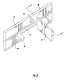
- FIG. 2 is a perspective view of the shielding frame as shown in FIG. 1.
- FIG. 3 is an enlarged perspective view of a portion of the shielding frame as shown in FIG. 2.
- FIG. 4 is a cross-sectional view taken along the line 4-4 of FIG. 3.
- FIG. 5 is a perspective view of the shielding lid as shown in FIG. 1.
- FIGs. 6 and 7 are enlarged views of embodiments of a wrap-around corner of the shielding frame as shown in FIG. 2.
- FIG. 8 is a more detailed schematic block diagram of an alternative embodiment of a handheld electronic device according to the invention.
- a handheld electronic device including a portable housing and a shielding container within the portable housing.
- the shielding container may include a shielding frame and a shielding lid carried thereby.
- a printed circuit board may be adjacent the shielding container.
- the shielding frame may include a base being generally planar and having at least one opening therein, a pair of opposing side walls integrally formed with the base and extending upwardly therefrom, and a pair of opposing end walls integrally formed with the base and extending upwardly therefrom.
- the shielding frame may include at least one intermediate partition wall integrally formed with the base and extending upwardly therefrom to define a plurality of container compartments.
- the partition wall may extend only partway between the opposing side walls to define at least one partition end gap therewith.
- the pair of opposing side walls includes at least one side wall stiffening feature incorporated therein.
- the at least one partition end gap may comprise a pair thereof, and the stiffening feature may include a respective stiffening feature adjacent each partition end gap.
- the side wall stiffening feature is preferably a radiused corner defined with adjacent portions of the base.
- the radiused corner may have a radius of less than about 5 mm or have a radius in a range of about 0.2 to 1.0 mm.
- each of the pair of partition end gaps may be less than about 1 mm to provide adequate shielding within the container compartments, and preferably is in a range of about 0.2 to 0.8 mm, and more preferably in a range of 0.5 to 0.7 mm.
- the printed circuit board may be a wireless transceiver printed circuit board, for example.
- the at least one intermediate partition wall may include a plurality of intermediate partition walls in some embodiments.
- the shielding frame may be devoid of welded or soldered joints between adjacent portions thereof.
- the shielding container may comprise an electrically conductive material and the shielding lid may be substantially continuous.
- a method aspect is directed to making a shielding container for at least one printed circuit board of a handheld electronic device.
- the method may include forming a shielding frame and forming a shielding lid carried by the shielding frame.
- Forming the shielding frame may include forming a planar base having at least one opening therein, integrally forming a pair of opposing side walls with the base and extending upwardly therefrom, and integrally forming a pair of opposing end walls with the base and extending upwardly therefrom.
- the method may include integrally forming at least one intermediate partition wall with the base and extending upwardly therefrom to define a plurality of container compartments, the at least one partition wall may also extend only partway between the opposing side walls to define at least one partition end gap therewith.
- At least one side wall stiffening feature may be formed in the pair of opposing side walls.
- the at least one partition end gap may comprise a pair thereof, and forming the at least one stiffening feature may include forming a respective stiffening feature adjacent each partition end gap. Forming the at least one side wall stiffening feature may include forming a radiused corner defined with adjacent portions of the base.
- a handheld electronic device 10 illustratively includes a portable housing and a shielding container 14 within the portable housing comprising upper and lower housing portions 11, 12.
- the shielding container 14 includes a shielding frame 16 and a shielding lid 17 carried thereby.
- the shielding lid 17 may be substantially continuous and attached to the shielding frame 16 as will be appreciated by those skilled in the art.
- a plurality of tabs 19 are positioned along flanges of the shielding lid 17 to be aligned with attaching holes 21 along the opposing side walls 24, 26 and end walls 28, 30 of the shielding frame 16, discussed below, thereby securing the shielding lid 17 to the shielding frame 16.
- a printed circuit board 18 is adjacent the shielding container 14, such as a wireless transceiver printed circuit board, for example.
- the shielding frame 16 includes a generally planar base 20 with a plurality of openings 22a-22d therein, a pair of opposing side walls 24, 26 integrally formed with the base and extending upwardly therefrom, and a pair of opposing end walls 28, 30 integrally formed with the base and extending upwardly therefrom. Also, the shielding frame 16 includes an intermediate partition wall 32 integrally formed with the base 20 and extending upwardly therefrom to define a pair of container compartments 34, 36. The partition wall 32 extends only partway between the opposing side walls 24, 26 to define a pair of partition end gap 38, 40 therewith. In the illustrated embodiment, a second partition wall 39 may extend upwardly from the base 20 and define only a single partition end gap 41.
- Each of the pair of partition end gaps 38, 40 may have a dimension d less than about 1 mm to provide adequate shielding within the container compartments yet facilitating manufacturing.
- the gap dimension d may preferably be in a range of about 0.2 to 0.8 mm, and more preferably in a range of 0.5 to 0.7 mm. Providing the pair of partition end gaps d in these ranges also contributes to the pair of opposing side walls 24, 26 imparting a sufficient stiffness to the shield frame 16.
- the pair of opposing side walls 24, 26 includes at least one side wall stiffening feature 50 incorporated therein, adjacent the partition end gap 38.
- the side wall stiffening feature is illustratively provided by a radiused corner 46 defined with adjacent portions of the base 20.
- the radiused corner 46 may have a radius R of less than about 5 mm or have a radius in a range of about 0.2 to 1.0 mm.
- the radiused corner may be used adjacent the other partition end gaps, 40, 41 as will be appreciated by those skilled in the art.
- the stiffening features may help yield a sufficient coplanarity of the base 20, such as within 0.1 ⁇ 0.15 mm, for example, so to avoid the need to solder adjacent portions of the shielding frame 16, as will also be appreciated by those skilled in the art. Accordingly, the shielding frame 16 may be devoid of welded or soldered joints between adjacent portions thereof.
- the shielding container 14 may comprise an electrically conductive material such as a stamped and folded copper sheet.
- the second partition wall 39, along with the offset side wall 25, may define a relatively smaller or more narrow container compartment 52.
- a wrap-around corner 54 is defined between the second partition wall 39 and the side wall 24.
- the side wall 24 preferably includes a corner extension 58 that is perpendicular to the side wall 24 and in-line with the second partition wall 39.
- the corner extension 58 extends to adjacent the second partition wall 39 with a gap 56 therebetween.
- the wrap-around corner 54' includes the corner extension 58 along with an offset side wall extension 60, of the offset side wall 25', between the corner extension 58 and the second partition wall 39.
- the gap 56 is between the offset side wall extension 60 and the second partition wall 39.
- the embodiment illustrated in FIG. 6 also includes the radiused corner 46 as a stiffening feature defined between the second partition wall 39 and adjacent portions of the base 20.
- a method aspect is directed to making a shielding container 14 for a printed circuit board 18 of a handheld electronic device 10.
- the method includes forming a shielding frame 16 and forming a shielding lid 17 carried by the shielding frame.
- Forming the shielding frame 16 includes forming a planar base 20 having at least one opening 22 therein, integrally forming a pair of opposing side walls 24, 26 with the base and extending upwardly therefrom, and integrally forming a pair of opposing end walls 28, 30 with the base and extending upwardly therefrom.
- the method includes integrally forming an intermediate partition wall 32 with the base 20 and extending upwardly therefrom to define a plurality of container compartments 34, 36.
- the partition wall 32 may also extend only partway between the opposing side walls 24, 26 to define one or a pair of partition end gaps therewith.
- the device 1000 illustratively includes a housing 1200, a keypad 1400 and an output device 1600.
- the output device shown is a display 1600, which is preferably a full graphic LCD. Other types of output devices may alternatively be utilized.
- a processing device 1800 is contained within the housing 1200 and is coupled between the keypad 1400 and the display 1600. The processing device 1800 controls the operation of the display 1600, as well as the overall operation of the mobile device 1000, in response to actuation of keys on the keypad 1400 by the user.
- the housing 1200 may be elongated vertically, or may take on other sizes and shapes (including clamshell housing structures).
- the keypad may include a mode selection key, or other hardware or software for switching between text entry and telephony entry.
- FIG. 8 In addition to the processing device 1800, other parts of the mobile device 1000 are shown schematically in FIG. 8. These include a communications subsystem 1001; a short-range communications subsystem 1020; the keypad 1400 and the display 1600, along with other input/output devices 1060, 1080, 1100 and 1120; as well as memory devices 1160, 1180 and various other device subsystems 1201.
- the mobile device 1000 is preferably a two-way RF communications device having voice and data communications capabilities.
- the mobile device 1000 preferably has the capability to communicate with other computer systems via the Internet.
- Operating system software executed by the processing device 1800 is preferably stored in a persistent store, such as the flash memory 1160, but may be stored in other types of memory devices, such as a read only memory (ROM) or similar storage element.
- system software, specific device applications, or parts thereof may be temporarily loaded into a volatile store, such as the random access memory (RAM) 1180. Communications signals received by the mobile device may also be stored in the RAM 1180.
- the processing device 1800 in addition to its operating system functions, enables execution of software applications 1300A-1300N on the device 1000.
- a predetermined set of applications that control basic device operations, such as data and voice communications 1300A and 1300B, may be installed on the device 1000 during manufacture.
- a personal information manager (PIM) application may be installed during manufacture.
- the PIM is preferably capable of organizing and managing data items, such as e-mail, calendar events, voice mails, appointments, and task items.
- the PIM application is also preferably capable of sending and receiving data items via a wireless network 1401.
- the PIM data items are seamlessly integrated, synchronized and updated via the wireless network 1401 with the device user's corresponding data items stored or associated with a host computer system.
- the communications subsystem 1001 includes a receiver 1500, a transmitter 1520, and one or more antennas 1540 and 1560.
- the communications subsystem 1001 also includes a processing module, such as a digital signal processor (DSP) 1580, and local oscillators (LOs) 1601.
- DSP digital signal processor
- LOs local oscillators
- a mobile device 1000 may include a communications subsystem 1001 designed to operate with the Mobitex TM , Data TAC TM or General Packet Radio Service (GPRS) mobile data communications networks, and also designed to operate with any of a variety of voice communications networks, such as AMPS, TDMA, CDMA, PCS, GSM, etc. Other types of data and voice networks, both separate and integrated, may also be utilized with the mobile device 1000.
- a communications subsystem 1001 designed to operate with the Mobitex TM , Data TAC TM or General Packet Radio Service (GPRS) mobile data communications networks, and also designed to operate with any of a variety of voice communications networks, such as AMPS, TDMA, CDMA, PCS, GSM, etc.
- voice communications networks such as AMPS, TDMA, CDMA, PCS, GSM, etc.
- Other types of data and voice networks, both separate and integrated, may also be utilized with the mobile device 1000.
- Network access requirements vary depending upon the type of communication system. For example, in the Mobitex and DataTAC networks, mobile devices are registered on the network using a unique personal identification number or PIN associated with each device. In GPRS networks, however, network access is associated with a subscriber or user of a device. A GPRS device therefore requires a subscriber identity module, commonly referred to as a SIM card, in order to operate on a GPRS network.
- SIM card subscriber identity module
- the mobile device 1000 may send and receive communications signals over the communication network 1401.
- Signals received from the communications network 1401 by the antenna 1540 are routed to the receiver 1500, which provides for signal amplification, frequency down conversion, filtering, channel selection, etc., and may also provide analog to digital conversion. Analog-to-digital conversion of the received signal allows the DSP 1580 to perform more complex communications functions, such as demodulation and decoding.
- signals to be transmitted to the network 1401 are processed (e.g. modulated and encoded) by the DSP 1580 and are then provided to the transmitter 1520 for digital to analog conversion, frequency up conversion, filtering, amplification and transmission to the communication network 1401 (or networks) via the antenna 1560.
- the DSP 1580 provides for control of the receiver 1500 and the transmitter 1520. For example, gains applied to communications signals in the receiver 1500 and transmitter 1520 may be adaptively controlled through automatic gain control algorithms implemented in the DSP 1580.
- a received signal such as a text message or web page download
- the communications subsystem 1001 is input to the processing device 1800.
- the received signal is then further processed by the processing device 1800 for an output to the display 1600, or alternatively to some other auxiliary I/O device 1060.
- a device user may also compose data items, such as e-mail messages, using the keypad 1400 and/or some other auxiliary I/O device 1060, such as a touchpad, a rocker switch, a thumb-wheel, or some other type of input device.
- the composed data items may then be transmitted over the communications network 1401 via the communications subsystem 1001.
- a voice communications mode In a voice communications mode, overall operation of the device is substantially similar to the data communications mode, except that received signals are output to a speaker 1100, and signals for transmission are generated by a microphone 1120.
- Alternative voice or audio I/O subsystems such as a voice message recording subsystem, may also be implemented on the device 1000.
- the display 1600 may also be utilized in voice communications mode, for example to display the identity of a calling party, the duration of a voice call, or other voice call related information.
- the short-range communications subsystem enables communication between the mobile device 1000 and other proximate systems or devices, which need not necessarily be similar devices.
- the short-range communications subsystem may include an infrared device and associated circuits and components, or a Bluetooth TM communications module to provide for communication with similarly-enabled systems and devices.
Landscapes
- Engineering & Computer Science (AREA)
- Microelectronics & Electronic Packaging (AREA)
- Shielding Devices Or Components To Electric Or Magnetic Fields (AREA)
- Telephone Set Structure (AREA)
- Electric Clocks (AREA)
Abstract
Description
- The present invention relates to the field of mobile communications, and, more particularly, to shielding within a mobile communication device and related methods.
- Cellular communication systems continue to grow in popularity and have become an integral part of both personal and business communications. Cellular telephones allow users to place and receive phone calls most anywhere they travel. Moreover, as cellular telephone technology has increased, so too has the functionality of cellular devices. For example, many cellular devices now incorporate Personal Digital Assistant (PDA) features such as calendars, address books, task lists, calculators, memo and writing programs, etc. These multifunction devices usually allow users to wirelessly send and receive electronic mail (email) messages and access the internet via a cellular network and/or a wireless local area network (WLAN), for example.
- As the functionality of cellular communications devices continues to increase, so too does the demand for smaller devices that are easier and more convenient for users to carry. As any circuit board and electronic components thereon are reduced in size and placed closer together, including antenna and microphone components, various electronic components can pick up energy and create interference within the system. For example, an internal surface mounted microphone could pick up energy directly from a power amplifier or from the radiated energy emitted by an antenna. This unwanted reception of energy from respective power amplifiers and antennae may be particularly problematic in a packet burst transmission as part of a Global System for Mobile communications (GSM) system, including the 450 MHz, 900 MHz, 1800 MHz and 1900 MHz frequency bands.
- Other interfering signals can be generated when the liquid crystal display (LCD) in some mobile wireless communications devices radiates radio frequency (RF) interfering energy and degrades receiver sensitivity. This may be problematic where the interfering energy is generated by the microprocessor or central processing unit (CPU) of a wireless mobile communications device and fed into the LCD lines, along with interfering energy generated by the LCD itself. Other problems may occur when the interfering radio frequency (RF) energy is coupled to the mobile wireless communications device causing audio break through tests to fail for both the uplink and downlink. Even the keyboard circuits can create unwanted interference problems. For example, the radio frequency receiver sensitivity is often degraded by the electromagnetic interference (EMI) of digital harmonics from the microprocessor or CPU via the keyboard because of the resulting loop formed by any keyboard circuits. In some instances, strong RF energy, for example, such as the transmitted power from the radio via the antenna interferes with or couples to the microprocessor or CPU input/output (I/O) lines of a mobile wireless communications device through the keyboard Key-In and Key-Out lines and causes a reset of the microprocessor or CPU.
- A shielding container can protect components on a printed circuit board (PCB), preferably for a cellular phone, against interference from other components due to EMI. A shielding container covers a number of electronic components on a printed circuit board, and thereby protects these components from disturbing other electronic components on the printed circuit board. The use of shielding containers is well known because GSM phones have printed circuit boards equipped with different components that may disturb each other if they are not shielded from each other.
- A first type of shielding container includes one entire box shaped piece soldered onto the printed circuit board. This type of shielding container does not permit access to components covered by the shielding container, which makes it very difficult to repair or inspect any of the components covered or shielded by the shielding container. An alternative is having holes or apertures to let the heat in to solder the components at the same time as the shielding container.
- A second type of shielding container includes two pieces, one frame and one lid. The lid is snapped onto the frame and can be removed from the frame, which is soldered onto the printed circuit board, to enable repairing or inspection of the components shielded by the shielding can. The second type may be attached to the printed circuit board in different ways. One way is to solder the frame onto the printed circuit board first and then attach the lid to the frame. Another way is to snap the lid onto the frame and solder the assembly onto the printed circuit board, but then there is a need for holes or apertures in the lid to let in the heat during soldering. Otherwise the components covered or shielded by the shielding container will not be properly soldered since the heat cannot reach the components. It is preferable to solder the frame with the lid attached to save work operations. However, according to the prior art there may be problems getting a good solder joint, when using a pre-joined shielding container.
-
U.S. Patent No. 5,895,884 to Davidson is directed to a shielding device with a push fit lid. The shielding device is formed from two unitary pieces, one of which is a generally planar member taking the form of a lid and the other piece takes the form of a side wall member which is adapted for mounting to a substrate surface on which is mounted circuit elements. The two pieces together combine to create the shielding device for inhibiting the passage of electromagnetic radiation to and/or from a group of circuit elements. The lid may have flanges for connection onto the side wall member and the side wall member may have intersecting dividing walls disposed internally thereof. -
U.S. Patent No. 6,600,663 to Koleda is directed to a shielding can for a printed circuit which includes a frame with side walls and a lid with increased flexibility from slits on the sides of the lid. These slits enable a flexible contraction, when soldering the shielding can onto the printed circuit board. -
U.S. Patent No. 6,137,051 to Bundza is directed to an electromagnetic interference and compatibility (EMI/EMC) shielding enclosure for a printed circuit board (PCB) or other electronic components that has a conductive plastic top housing portion and a conductive bottom housing portion. The top housing portion has projecting fingers integral therewith. The bottom housing portion has an inner surface with walls projecting therefrom for substantially encompassing the PCB. When the enclosure is assembled, the PCB is located between the top housing portion and the bottom housing portion, the fingers from the top housing portion surround at least a major portion of the PCB and the fingers physically contact the bottom housing portion or are sufficiently close for capacitive coupling. - There is still a need for a handheld electronic device including a multi-compartment shielding container with inter-compartment shielding and sufficient stiffness to be used for printed circuit boards within the electronic device.
- FIG. 1 is an exploded end view of a handheld electronic device according to the present invention.
- FIG. 2 is a perspective view of the shielding frame as shown in FIG. 1.
- FIG. 3 is an enlarged perspective view of a portion of the shielding frame as shown in FIG. 2.
- FIG. 4 is a cross-sectional view taken along the line 4-4 of FIG. 3.
- FIG. 5 is a perspective view of the shielding lid as shown in FIG. 1.
- FIGs. 6 and 7 are enlarged views of embodiments of a wrap-around corner of the shielding frame as shown in FIG. 2.
- FIG. 8 is a more detailed schematic block diagram of an alternative embodiment of a handheld electronic device according to the invention.
- The present invention will now be described more fully hereinafter with reference to the accompanying drawings, in which preferred embodiments of the invention are shown. This invention may, however, be embodied in many different forms and should not be construed as limited to the embodiments set forth herein. Rather, these embodiments are provided so that this disclosure will be thorough and complete, and will fully convey the scope of the invention to those skilled in the art. Like numbers refer to like elements throughout.
- In view of the foregoing background, it is therefore an object of the present invention to provide a handheld electronic device including a multi-compartment shielding container with inter-compartment shielding and sufficient stiffness. This and other objects, features, and advantages in accordance with the present invention are provided by a handheld electronic device including a portable housing and a shielding container within the portable housing. The shielding container may include a shielding frame and a shielding lid carried thereby. A printed circuit board may be adjacent the shielding container. The shielding frame may include a base being generally planar and having at least one opening therein, a pair of opposing side walls integrally formed with the base and extending upwardly therefrom, and a pair of opposing end walls integrally formed with the base and extending upwardly therefrom. Also, the shielding frame may include at least one intermediate partition wall integrally formed with the base and extending upwardly therefrom to define a plurality of container compartments. The partition wall may extend only partway between the opposing side walls to define at least one partition end gap therewith.
- Preferably, the pair of opposing side walls includes at least one side wall stiffening feature incorporated therein. The at least one partition end gap may comprise a pair thereof, and the stiffening feature may include a respective stiffening feature adjacent each partition end gap. The side wall stiffening feature is preferably a radiused corner defined with adjacent portions of the base. For example, the radiused corner may have a radius of less than about 5 mm or have a radius in a range of about 0.2 to 1.0 mm. Also, each of the pair of partition end gaps may be less than about 1 mm to provide adequate shielding within the container compartments, and preferably is in a range of about 0.2 to 0.8 mm, and more preferably in a range of 0.5 to 0.7 mm.
- The printed circuit board may be a wireless transceiver printed circuit board, for example. The at least one intermediate partition wall may include a plurality of intermediate partition walls in some embodiments. The shielding frame may be devoid of welded or soldered joints between adjacent portions thereof. In addition, the shielding container may comprise an electrically conductive material and the shielding lid may be substantially continuous.
- A method aspect is directed to making a shielding container for at least one printed circuit board of a handheld electronic device. The method may include forming a shielding frame and forming a shielding lid carried by the shielding frame. Forming the shielding frame may include forming a planar base having at least one opening therein, integrally forming a pair of opposing side walls with the base and extending upwardly therefrom, and integrally forming a pair of opposing end walls with the base and extending upwardly therefrom. Also, the method may include integrally forming at least one intermediate partition wall with the base and extending upwardly therefrom to define a plurality of container compartments, the at least one partition wall may also extend only partway between the opposing side walls to define at least one partition end gap therewith. At least one side wall stiffening feature may be formed in the pair of opposing side walls.
- The at least one partition end gap may comprise a pair thereof, and forming the at least one stiffening feature may include forming a respective stiffening feature adjacent each partition end gap. Forming the at least one side wall stiffening feature may include forming a radiused corner defined with adjacent portions of the base.
- [0024] Referring initially to FIGS. 1-5, a handheld
electronic device 10 illustratively includes a portable housing and a shieldingcontainer 14 within the portable housing comprising upper andlower housing portions container 14 includes a shieldingframe 16 and a shieldinglid 17 carried thereby. The shieldinglid 17 may be substantially continuous and attached to the shieldingframe 16 as will be appreciated by those skilled in the art. A plurality oftabs 19 are positioned along flanges of the shieldinglid 17 to be aligned with attachingholes 21 along the opposingside walls walls frame 16, discussed below, thereby securing the shieldinglid 17 to the shieldingframe 16. A printedcircuit board 18 is adjacent the shieldingcontainer 14, such as a wireless transceiver printed circuit board, for example. - The shielding
frame 16 includes a generallyplanar base 20 with a plurality ofopenings 22a-22d therein, a pair of opposingside walls end walls frame 16 includes anintermediate partition wall 32 integrally formed with thebase 20 and extending upwardly therefrom to define a pair of container compartments 34, 36. Thepartition wall 32 extends only partway between the opposingside walls partition end gap second partition wall 39 may extend upwardly from thebase 20 and define only a singlepartition end gap 41. - Each of the pair of
partition end gaps side walls shield frame 16. - Referring more specifically to FIGS. 3 and 4, the pair of opposing
side walls wall stiffening feature 50 incorporated therein, adjacent thepartition end gap 38. The side wall stiffening feature is illustratively provided by aradiused corner 46 defined with adjacent portions of thebase 20. For example, theradiused corner 46 may have a radius R of less than about 5 mm or have a radius in a range of about 0.2 to 1.0 mm. The radiused corner may be used adjacent the other partition end gaps, 40, 41 as will be appreciated by those skilled in the art. The stiffening features may help yield a sufficient coplanarity of thebase 20, such as within 0.1~0.15 mm, for example, so to avoid the need to solder adjacent portions of the shieldingframe 16, as will also be appreciated by those skilled in the art. Accordingly, the shieldingframe 16 may be devoid of welded or soldered joints between adjacent portions thereof. The shieldingcontainer 14 may comprise an electrically conductive material such as a stamped and folded copper sheet. - Referring more specifically to FIGs. 2, 6 and 7, the
second partition wall 39, along with the offsetside wall 25, may define a relatively smaller or morenarrow container compartment 52. As such, a wrap-aroundcorner 54 is defined between thesecond partition wall 39 and theside wall 24. Theside wall 24 preferably includes acorner extension 58 that is perpendicular to theside wall 24 and in-line with thesecond partition wall 39. In one embodiment (FIG. 6), thecorner extension 58 extends to adjacent thesecond partition wall 39 with agap 56 therebetween. In an alternative embodiment (FIG. 7), the wrap-around corner 54' includes thecorner extension 58 along with an offsetside wall extension 60, of the offset side wall 25', between thecorner extension 58 and thesecond partition wall 39. In this embodiment, thegap 56 is between the offsetside wall extension 60 and thesecond partition wall 39. The embodiment illustrated in FIG. 6 also includes the radiusedcorner 46 as a stiffening feature defined between thesecond partition wall 39 and adjacent portions of thebase 20. - A method aspect is directed to making a shielding
container 14 for a printedcircuit board 18 of a handheldelectronic device 10. The method includes forming a shieldingframe 16 and forming a shieldinglid 17 carried by the shielding frame. Forming the shieldingframe 16 includes forming aplanar base 20 having at least one opening 22 therein, integrally forming a pair of opposingside walls end walls intermediate partition wall 32 with thebase 20 and extending upwardly therefrom to define a plurality of container compartments 34, 36. Thepartition wall 32 may also extend only partway between the opposingside walls - One example of a hand-held mobile
wireless communications device 1000 that may be used is further described in the example below with reference to FIG. 8. Thedevice 1000 illustratively includes ahousing 1200, akeypad 1400 and anoutput device 1600. The output device shown is adisplay 1600, which is preferably a full graphic LCD. Other types of output devices may alternatively be utilized. Aprocessing device 1800 is contained within thehousing 1200 and is coupled between thekeypad 1400 and thedisplay 1600. Theprocessing device 1800 controls the operation of thedisplay 1600, as well as the overall operation of themobile device 1000, in response to actuation of keys on thekeypad 1400 by the user. - The
housing 1200 may be elongated vertically, or may take on other sizes and shapes (including clamshell housing structures). The keypad may include a mode selection key, or other hardware or software for switching between text entry and telephony entry. - In addition to the
processing device 1800, other parts of themobile device 1000 are shown schematically in FIG. 8. These include acommunications subsystem 1001; a short-range communications subsystem 1020; thekeypad 1400 and thedisplay 1600, along with other input/output devices memory devices other device subsystems 1201. Themobile device 1000 is preferably a two-way RF communications device having voice and data communications capabilities. In addition, themobile device 1000 preferably has the capability to communicate with other computer systems via the Internet. - Operating system software executed by the
processing device 1800 is preferably stored in a persistent store, such as theflash memory 1160, but may be stored in other types of memory devices, such as a read only memory (ROM) or similar storage element. In addition, system software, specific device applications, or parts thereof, may be temporarily loaded into a volatile store, such as the random access memory (RAM) 1180. Communications signals received by the mobile device may also be stored in theRAM 1180. - The
processing device 1800, in addition to its operating system functions, enables execution ofsoftware applications 1300A-1300N on thedevice 1000. A predetermined set of applications that control basic device operations, such as data andvoice communications device 1000 during manufacture. In addition, a personal information manager (PIM) application may be installed during manufacture. The PIM is preferably capable of organizing and managing data items, such as e-mail, calendar events, voice mails, appointments, and task items. The PIM application is also preferably capable of sending and receiving data items via awireless network 1401. Preferably, the PIM data items are seamlessly integrated, synchronized and updated via thewireless network 1401 with the device user's corresponding data items stored or associated with a host computer system. Communication functions, including data and voice communications, are performed through thecommunications subsystem 1001, and possibly through the short-range communications subsystem. Thecommunications subsystem 1001 includes areceiver 1500, atransmitter 1520, and one ormore antennas communications subsystem 1001 also includes a processing module, such as a digital signal processor (DSP) 1580, and local oscillators (LOs) 1601. The specific design and implementation of thecommunications subsystem 1001 is dependent upon the communications network in which themobile device 1000 is intended to operate. For example, amobile device 1000 may include acommunications subsystem 1001 designed to operate with the Mobitex™, Data TAC™ or General Packet Radio Service (GPRS) mobile data communications networks, and also designed to operate with any of a variety of voice communications networks, such as AMPS, TDMA, CDMA, PCS, GSM, etc. Other types of data and voice networks, both separate and integrated, may also be utilized with themobile device 1000. - Network access requirements vary depending upon the type of communication system. For example, in the Mobitex and DataTAC networks, mobile devices are registered on the network using a unique personal identification number or PIN associated with each device. In GPRS networks, however, network access is associated with a subscriber or user of a device. A GPRS device therefore requires a subscriber identity module, commonly referred to as a SIM card, in order to operate on a GPRS network.
- When required network registration or activation procedures have been completed, the
mobile device 1000 may send and receive communications signals over thecommunication network 1401. Signals received from thecommunications network 1401 by theantenna 1540 are routed to thereceiver 1500, which provides for signal amplification, frequency down conversion, filtering, channel selection, etc., and may also provide analog to digital conversion. Analog-to-digital conversion of the received signal allows theDSP 1580 to perform more complex communications functions, such as demodulation and decoding. In a similar manner, signals to be transmitted to thenetwork 1401 are processed (e.g. modulated and encoded) by theDSP 1580 and are then provided to thetransmitter 1520 for digital to analog conversion, frequency up conversion, filtering, amplification and transmission to the communication network 1401 (or networks) via theantenna 1560. - In addition to processing communications signals, the
DSP 1580 provides for control of thereceiver 1500 and thetransmitter 1520. For example, gains applied to communications signals in thereceiver 1500 andtransmitter 1520 may be adaptively controlled through automatic gain control algorithms implemented in theDSP 1580. - In a data communications mode, a received signal, such as a text message or web page download, is processed by the
communications subsystem 1001 and is input to theprocessing device 1800. The received signal is then further processed by theprocessing device 1800 for an output to thedisplay 1600, or alternatively to some other auxiliary I/O device 1060. A device user may also compose data items, such as e-mail messages, using thekeypad 1400 and/or some other auxiliary I/O device 1060, such as a touchpad, a rocker switch, a thumb-wheel, or some other type of input device. The composed data items may then be transmitted over thecommunications network 1401 via thecommunications subsystem 1001. - In a voice communications mode, overall operation of the device is substantially similar to the data communications mode, except that received signals are output to a
speaker 1100, and signals for transmission are generated by amicrophone 1120. Alternative voice or audio I/O subsystems, such as a voice message recording subsystem, may also be implemented on thedevice 1000. In addition, thedisplay 1600 may also be utilized in voice communications mode, for example to display the identity of a calling party, the duration of a voice call, or other voice call related information. - The short-range communications subsystem enables communication between the
mobile device 1000 and other proximate systems or devices, which need not necessarily be similar devices. For example, the short-range communications subsystem may include an infrared device and associated circuits and components, or a Bluetooth™ communications module to provide for communication with similarly-enabled systems and devices. - Many modifications and other embodiments of the invention will come to the mind of one skilled in the art having the benefit of the teachings presented in the foregoing descriptions and the associated drawings. Therefore, it is understood that the invention is not to be limited to the specific embodiments disclosed, and that modifications and embodiments are intended to be included within the scope of the appended claims.
Claims (18)
- A handheld electronic device comprising:a portable housing;a shielding container within said portable housing and comprising a shielding frame and a shielding lid carried thereby;at least one printed circuit board adjacent said shielding container;said shielding frame comprisinga base being generally planar and having at least one opening therein,a pair of opposing side walls integrally formed with said base and extending upwardly therefrom,a pair of opposing end walls integrally formed with said base and extending upwardly therefrom,at least one intermediate partition wall integrally formed with said base and extending upwardly therefrom to define a plurality of container compartments, said at least one partition wall also extending only partway between said opposing side walls to define at least one partition end gap therewith.
- The handheld electronic device according to Claim 1 wherein said pair of opposing side walls comprises at least one side wall stiffening feature incorporated therein.
- The handheld electronic device according to Claim 2 wherein said at least one partition end gap comprises a pair thereof; and wherein said at least one stiffening feature comprises a respective stiffening feature adjacent each partition end gap.
- The handheld electronic device according to Claim 2 wherein said at least one side wall stiffening feature comprises a radiused corner defined with adjacent portions of said base.
- The handheld electronic device according to Claim 4 wherein said radiused corner has a radius of less than about 5 mm.
- The handheld electronic device according to Claim 1 wherein each of said pair of partition end gaps is less than about 1 mm.
- The handheld electronic device according to Claim 1 wherein said at least one printed circuit board comprises a wireless transceiver printed circuit board.
- The handheld electronic device according to Claim 1 wherein said at least one intermediate partition wall comprises a plurality of intermediate partition walls.
- The handheld electronic device according to Claim 1 wherein said shielding frame is devoid of welded or soldered joints between adjacent portions thereof.
- The handheld electronic device according to Claim 1 further comprising a wrap-around corner defined between said at least one intermediate partition wall and at least one opposing side wall.
- A shielding container for at least one printed circuit board of a handheld electronic device, the shielding container comprising:a shielding frame; anda shielding lid carried by the shielding frame; said shielding frame comprisinga planar base having at least one opening therein,a pair of opposing side walls integrally formed with said base and extending upwardly therefrom,a pair of opposing end walls integrally formed with said base and extending upwardly therefrom,at least one intermediate partition wall integrally formed with said base and extending upwardly therefrom to define a plurality of container compartments, said at least one partition wall also extending only partway between said opposing side walls to define at least one partition end gap therewith, andsaid pair of opposing side walls comprising at least one side wall stiffening feature incorporated therein.
- The shielding container according to Claim 11 wherein said at least one partition end gap comprises a pair thereof; and wherein least one stiffening feature comprises a respective stiffening feature adjacent each partition end gap.
- The shielding container according to Claim 12 wherein said at least one side wall stiffening feature comprises a radiused corner defined with adjacent portions of said base.
- The shielding container according to Claim 13 wherein said radiused corner has a radius of less than about 5 mm.
- A method for making a shielding container for at least one printed circuit board of a handheld electronic device, the method comprising:forming a shielding frame; andforming a shielding lid carried by the shielding frame;forming the shielding frame comprisingforming a planar base having at least one opening therein,integrally forming a pair of opposing side walls with the base and extending upwardly therefrom,integrally forming a pair of opposing end walls with the base and extending upwardly therefrom,integrally forming at least one intermediate partition wall with the base and extending upwardly therefrom to define a plurality of container compartments, the at least one partition wall also extending only partway between the opposing side walls to define at least one partition end gap therewith, andforming at least one side wall stiffening feature in the pair of opposing side walls.
- The method according to Claim 15 wherein the at least one partition end gap comprises a pair thereof; and wherein forming the at least one stiffening feature comprises forming a respective stiffening feature adjacent each partition end gap.
- The method according to Claim 15 wherein forming the at least one side wall stiffening feature comprises forming a radiused corner defined with adjacent portions of the base.
- The method according to Claim 17 wherein said radiused corner has a radius of less than about 5 mm.
Priority Applications (6)
| Application Number | Priority Date | Filing Date | Title |
|---|---|---|---|
| EP06119181A EP1890526B1 (en) | 2006-08-18 | 2006-08-18 | Handheld electronic device including multi-compartment shielding container and associated methods |
| DE602006009803T DE602006009803D1 (en) | 2006-08-18 | 2006-08-18 | Portable electronic device containing multi-chamber electromagnetic shielding and associated methods |
| AT06119181T ATE445994T1 (en) | 2006-08-18 | 2006-08-18 | PORTABLE ELECTRONIC DEVICE INCLUDING MULTI-CHAMBER ELECTROMAGNETIC SHIELDING AND METHODS THEREOF |
| CA002594110A CA2594110C (en) | 2006-08-18 | 2007-08-02 | Handheld electronic device including multi-compartment shielding container and associated methods |
| CN201510174977.XA CN104797125B (en) | 2006-08-18 | 2007-08-15 | Hand-hold electronic equipments and correlation technique including multi-compartment shielding container |
| CNA200710149455XA CN101127791A (en) | 2006-08-18 | 2007-08-15 | Handheld electronic device including multi-compartment shielded container and related methods |
Applications Claiming Priority (1)
| Application Number | Priority Date | Filing Date | Title |
|---|---|---|---|
| EP06119181A EP1890526B1 (en) | 2006-08-18 | 2006-08-18 | Handheld electronic device including multi-compartment shielding container and associated methods |
Publications (2)
| Publication Number | Publication Date |
|---|---|
| EP1890526A1 true EP1890526A1 (en) | 2008-02-20 |
| EP1890526B1 EP1890526B1 (en) | 2009-10-14 |
Family
ID=37911867
Family Applications (1)
| Application Number | Title | Priority Date | Filing Date |
|---|---|---|---|
| EP06119181A Active EP1890526B1 (en) | 2006-08-18 | 2006-08-18 | Handheld electronic device including multi-compartment shielding container and associated methods |
Country Status (5)
| Country | Link |
|---|---|
| EP (1) | EP1890526B1 (en) |
| CN (2) | CN101127791A (en) |
| AT (1) | ATE445994T1 (en) |
| CA (1) | CA2594110C (en) |
| DE (1) | DE602006009803D1 (en) |
Cited By (2)
| Publication number | Priority date | Publication date | Assignee | Title |
|---|---|---|---|---|
| JP2017501371A (en) * | 2013-10-01 | 2017-01-12 | オートリブ エー・エス・ピー・インク | Compact shield automotive radar module and method |
| GB2601333A (en) * | 2020-11-26 | 2022-06-01 | Continental Automotive Gmbh | Electromagnetic interference shield device |
Families Citing this family (2)
| Publication number | Priority date | Publication date | Assignee | Title |
|---|---|---|---|---|
| CN101578033B (en) * | 2008-05-09 | 2011-07-20 | 莱尔德电子材料(深圳)有限公司 | Shielding device and manufacturing method thereof |
| CN112469258B (en) * | 2020-10-28 | 2022-03-01 | 西安电子科技大学 | Double-gap electromagnetic shielding system, design method thereof and microwave circuit |
Citations (2)
| Publication number | Priority date | Publication date | Assignee | Title |
|---|---|---|---|---|
| US5731964A (en) * | 1995-05-23 | 1998-03-24 | Sony Corporation | Electromagnetic-wave shielding device |
| DE29913199U1 (en) * | 1999-07-28 | 1999-12-16 | Siemens AG, 80333 München | Shielding for an electrical assembly |
Family Cites Families (3)
| Publication number | Priority date | Publication date | Assignee | Title |
|---|---|---|---|---|
| US4370515A (en) * | 1979-12-26 | 1983-01-25 | Rockwell International Corporation | Electromagnetic interference |
| GB2297868B (en) * | 1995-02-07 | 1999-04-28 | Nokia Mobile Phones Ltd | A shielding device |
| US6624432B1 (en) * | 1999-10-12 | 2003-09-23 | Shielding For Electronics, Inc. | EMI containment apparatus |
-
2006
- 2006-08-18 DE DE602006009803T patent/DE602006009803D1/en active Active
- 2006-08-18 AT AT06119181T patent/ATE445994T1/en not_active IP Right Cessation
- 2006-08-18 EP EP06119181A patent/EP1890526B1/en active Active
-
2007
- 2007-08-02 CA CA002594110A patent/CA2594110C/en active Active
- 2007-08-15 CN CNA200710149455XA patent/CN101127791A/en active Pending
- 2007-08-15 CN CN201510174977.XA patent/CN104797125B/en active Active
Patent Citations (2)
| Publication number | Priority date | Publication date | Assignee | Title |
|---|---|---|---|---|
| US5731964A (en) * | 1995-05-23 | 1998-03-24 | Sony Corporation | Electromagnetic-wave shielding device |
| DE29913199U1 (en) * | 1999-07-28 | 1999-12-16 | Siemens AG, 80333 München | Shielding for an electrical assembly |
Cited By (2)
| Publication number | Priority date | Publication date | Assignee | Title |
|---|---|---|---|---|
| JP2017501371A (en) * | 2013-10-01 | 2017-01-12 | オートリブ エー・エス・ピー・インク | Compact shield automotive radar module and method |
| GB2601333A (en) * | 2020-11-26 | 2022-06-01 | Continental Automotive Gmbh | Electromagnetic interference shield device |
Also Published As
| Publication number | Publication date |
|---|---|
| CA2594110C (en) | 2009-10-13 |
| CA2594110A1 (en) | 2007-11-04 |
| DE602006009803D1 (en) | 2009-11-26 |
| EP1890526B1 (en) | 2009-10-14 |
| CN101127791A (en) | 2008-02-20 |
| ATE445994T1 (en) | 2009-10-15 |
| CN104797125A (en) | 2015-07-22 |
| CN104797125B (en) | 2018-06-08 |
Similar Documents
| Publication | Publication Date | Title |
|---|---|---|
| US8644033B2 (en) | Handheld electronic device including multi-compartment shielding container and associated methods | |
| US8446333B2 (en) | Mobile wireless communications device with reduced interfering RF energy into RF metal shield secured on circuit board | |
| US20110111810A1 (en) | Mobile wireless communications device with reduced microphone noise from radio frequency communications circuitry | |
| KR101092028B1 (en) | Mobile wireless communications device with antenna contact having reduced rf inductance | |
| WO2006024132A1 (en) | Mobile wireless communications device with reduced interfering energy into audio circuit and related methods | |
| WO2006024133A1 (en) | Mobile wireless communications device with reduced interfering energy from the display and related methods | |
| US20120256791A1 (en) | Mobile wireless communications device comprising a satellite positioning system antenna and electrically conductive director element therefor | |
| CA2594110C (en) | Handheld electronic device including multi-compartment shielding container and associated methods | |
| CA2668754C (en) | Mobile wireless communications device with rf immune charging contacts | |
| CA2596907C (en) | Mobile wireless communications device including an electrically conductive, electrically floating element and related methods | |
| CA2586100C (en) | Mobile wireless communications device with reduced interfering rf energy into rf metal shield secured on circuit board | |
| US20130194137A1 (en) | Mobile wireless communications device including rigid mechanical stiffener slot antenna and related methods | |
| EP2498335A1 (en) | Mobile wireless communications device including antenna assembly having shorted feed points and inductor-capacitor circuit and related methods |
Legal Events
| Date | Code | Title | Description |
|---|---|---|---|
| PUAI | Public reference made under article 153(3) epc to a published international application that has entered the european phase |
Free format text: ORIGINAL CODE: 0009012 |
|
| 17P | Request for examination filed |
Effective date: 20060821 |
|
| AK | Designated contracting states |
Kind code of ref document: A1 Designated state(s): AT BE BG CH CY CZ DE DK EE ES FI FR GB GR HU IE IS IT LI LT LU LV MC NL PL PT RO SE SI SK TR |
|
| AX | Request for extension of the european patent |
Extension state: AL BA HR MK YU |
|
| AKX | Designation fees paid |
Designated state(s): AT BE BG CH CY CZ DE DK EE ES FI FR GB GR HU IE IS IT LI LT LU LV MC NL PL PT RO SE SI SK TR |
|
| AXX | Extension fees paid |
Extension state: MK Payment date: 20080725 Extension state: BA Payment date: 20080725 Extension state: HR Payment date: 20080725 Extension state: RS Payment date: 20080725 Extension state: AL Payment date: 20080725 |
|
| GRAP | Despatch of communication of intention to grant a patent |
Free format text: ORIGINAL CODE: EPIDOSNIGR1 |
|
| GRAS | Grant fee paid |
Free format text: ORIGINAL CODE: EPIDOSNIGR3 |
|
| GRAA | (expected) grant |
Free format text: ORIGINAL CODE: 0009210 |
|
| AK | Designated contracting states |
Kind code of ref document: B1 Designated state(s): AT BE BG CH CY CZ DE DK EE ES FI FR GB GR HU IE IS IT LI LT LU LV MC NL PL PT RO SE SI SK TR |
|
| AX | Request for extension of the european patent |
Extension state: AL BA HR MK RS |
|
| REG | Reference to a national code |
Ref country code: GB Ref legal event code: FG4D |
|
| REG | Reference to a national code |
Ref country code: CH Ref legal event code: EP |
|
| REG | Reference to a national code |
Ref country code: IE Ref legal event code: FG4D |
|
| REF | Corresponds to: |
Ref document number: 602006009803 Country of ref document: DE Date of ref document: 20091126 Kind code of ref document: P |
|
| REG | Reference to a national code |
Ref country code: SE Ref legal event code: TRGR |
|
| LTIE | Lt: invalidation of european patent or patent extension |
Effective date: 20091014 |
|
| NLV1 | Nl: lapsed or annulled due to failure to fulfill the requirements of art. 29p and 29m of the patents act | ||
| PG25 | Lapsed in a contracting state [announced via postgrant information from national office to epo] |
Ref country code: PT Free format text: LAPSE BECAUSE OF FAILURE TO SUBMIT A TRANSLATION OF THE DESCRIPTION OR TO PAY THE FEE WITHIN THE PRESCRIBED TIME-LIMIT Effective date: 20100215 Ref country code: LT Free format text: LAPSE BECAUSE OF FAILURE TO SUBMIT A TRANSLATION OF THE DESCRIPTION OR TO PAY THE FEE WITHIN THE PRESCRIBED TIME-LIMIT Effective date: 20091014 Ref country code: IS Free format text: LAPSE BECAUSE OF FAILURE TO SUBMIT A TRANSLATION OF THE DESCRIPTION OR TO PAY THE FEE WITHIN THE PRESCRIBED TIME-LIMIT Effective date: 20100214 Ref country code: ES Free format text: LAPSE BECAUSE OF FAILURE TO SUBMIT A TRANSLATION OF THE DESCRIPTION OR TO PAY THE FEE WITHIN THE PRESCRIBED TIME-LIMIT Effective date: 20100125 |
|
| PG25 | Lapsed in a contracting state [announced via postgrant information from national office to epo] |
Ref country code: SI Free format text: LAPSE BECAUSE OF FAILURE TO SUBMIT A TRANSLATION OF THE DESCRIPTION OR TO PAY THE FEE WITHIN THE PRESCRIBED TIME-LIMIT Effective date: 20091014 Ref country code: PL Free format text: LAPSE BECAUSE OF FAILURE TO SUBMIT A TRANSLATION OF THE DESCRIPTION OR TO PAY THE FEE WITHIN THE PRESCRIBED TIME-LIMIT Effective date: 20091014 Ref country code: LV Free format text: LAPSE BECAUSE OF FAILURE TO SUBMIT A TRANSLATION OF THE DESCRIPTION OR TO PAY THE FEE WITHIN THE PRESCRIBED TIME-LIMIT Effective date: 20091014 |
|
| PG25 | Lapsed in a contracting state [announced via postgrant information from national office to epo] |
Ref country code: AT Free format text: LAPSE BECAUSE OF FAILURE TO SUBMIT A TRANSLATION OF THE DESCRIPTION OR TO PAY THE FEE WITHIN THE PRESCRIBED TIME-LIMIT Effective date: 20091014 Ref country code: BE Free format text: LAPSE BECAUSE OF FAILURE TO SUBMIT A TRANSLATION OF THE DESCRIPTION OR TO PAY THE FEE WITHIN THE PRESCRIBED TIME-LIMIT Effective date: 20091014 |
|
| PG25 | Lapsed in a contracting state [announced via postgrant information from national office to epo] |
Ref country code: RO Free format text: LAPSE BECAUSE OF FAILURE TO SUBMIT A TRANSLATION OF THE DESCRIPTION OR TO PAY THE FEE WITHIN THE PRESCRIBED TIME-LIMIT Effective date: 20091014 Ref country code: EE Free format text: LAPSE BECAUSE OF FAILURE TO SUBMIT A TRANSLATION OF THE DESCRIPTION OR TO PAY THE FEE WITHIN THE PRESCRIBED TIME-LIMIT Effective date: 20091014 Ref country code: DK Free format text: LAPSE BECAUSE OF FAILURE TO SUBMIT A TRANSLATION OF THE DESCRIPTION OR TO PAY THE FEE WITHIN THE PRESCRIBED TIME-LIMIT Effective date: 20091014 Ref country code: BG Free format text: LAPSE BECAUSE OF FAILURE TO SUBMIT A TRANSLATION OF THE DESCRIPTION OR TO PAY THE FEE WITHIN THE PRESCRIBED TIME-LIMIT Effective date: 20100114 |
|
| PLBE | No opposition filed within time limit |
Free format text: ORIGINAL CODE: 0009261 |
|
| STAA | Information on the status of an ep patent application or granted ep patent |
Free format text: STATUS: NO OPPOSITION FILED WITHIN TIME LIMIT |
|
| PG25 | Lapsed in a contracting state [announced via postgrant information from national office to epo] |
Ref country code: SK Free format text: LAPSE BECAUSE OF FAILURE TO SUBMIT A TRANSLATION OF THE DESCRIPTION OR TO PAY THE FEE WITHIN THE PRESCRIBED TIME-LIMIT Effective date: 20091014 Ref country code: CZ Free format text: LAPSE BECAUSE OF FAILURE TO SUBMIT A TRANSLATION OF THE DESCRIPTION OR TO PAY THE FEE WITHIN THE PRESCRIBED TIME-LIMIT Effective date: 20091014 |
|
| 26N | No opposition filed |
Effective date: 20100715 |
|
| PG25 | Lapsed in a contracting state [announced via postgrant information from national office to epo] |
Ref country code: GR Free format text: LAPSE BECAUSE OF FAILURE TO SUBMIT A TRANSLATION OF THE DESCRIPTION OR TO PAY THE FEE WITHIN THE PRESCRIBED TIME-LIMIT Effective date: 20100115 |
|
| PG25 | Lapsed in a contracting state [announced via postgrant information from national office to epo] |
Ref country code: MC Free format text: LAPSE BECAUSE OF NON-PAYMENT OF DUE FEES Effective date: 20100831 Ref country code: IT Free format text: LAPSE BECAUSE OF FAILURE TO SUBMIT A TRANSLATION OF THE DESCRIPTION OR TO PAY THE FEE WITHIN THE PRESCRIBED TIME-LIMIT Effective date: 20091014 |
|
| REG | Reference to a national code |
Ref country code: CH Ref legal event code: PL |
|
| PG25 | Lapsed in a contracting state [announced via postgrant information from national office to epo] |
Ref country code: CH Free format text: LAPSE BECAUSE OF NON-PAYMENT OF DUE FEES Effective date: 20100831 Ref country code: LI Free format text: LAPSE BECAUSE OF NON-PAYMENT OF DUE FEES Effective date: 20100831 |
|
| PG25 | Lapsed in a contracting state [announced via postgrant information from national office to epo] |
Ref country code: IE Free format text: LAPSE BECAUSE OF NON-PAYMENT OF DUE FEES Effective date: 20100818 |
|
| PG25 | Lapsed in a contracting state [announced via postgrant information from national office to epo] |
Ref country code: CY Free format text: LAPSE BECAUSE OF FAILURE TO SUBMIT A TRANSLATION OF THE DESCRIPTION OR TO PAY THE FEE WITHIN THE PRESCRIBED TIME-LIMIT Effective date: 20091014 |
|
| PG25 | Lapsed in a contracting state [announced via postgrant information from national office to epo] |
Ref country code: HU Free format text: LAPSE BECAUSE OF FAILURE TO SUBMIT A TRANSLATION OF THE DESCRIPTION OR TO PAY THE FEE WITHIN THE PRESCRIBED TIME-LIMIT Effective date: 20100415 Ref country code: NL Free format text: LAPSE BECAUSE OF FAILURE TO SUBMIT A TRANSLATION OF THE DESCRIPTION OR TO PAY THE FEE WITHIN THE PRESCRIBED TIME-LIMIT Effective date: 20091014 Ref country code: LU Free format text: LAPSE BECAUSE OF NON-PAYMENT OF DUE FEES Effective date: 20100818 |
|
| PG25 | Lapsed in a contracting state [announced via postgrant information from national office to epo] |
Ref country code: TR Free format text: LAPSE BECAUSE OF FAILURE TO SUBMIT A TRANSLATION OF THE DESCRIPTION OR TO PAY THE FEE WITHIN THE PRESCRIBED TIME-LIMIT Effective date: 20091014 |
|
| REG | Reference to a national code |
Ref country code: DE Ref legal event code: R082 Ref document number: 602006009803 Country of ref document: DE Representative=s name: MERH-IP MATIAS ERNY REICHL HOFFMANN, DE |
|
| REG | Reference to a national code |
Ref country code: DE Ref legal event code: R082 Ref document number: 602006009803 Country of ref document: DE Representative=s name: MERH-IP MATIAS ERNY REICHL HOFFMANN, DE Effective date: 20140925 Ref country code: DE Ref legal event code: R081 Ref document number: 602006009803 Country of ref document: DE Owner name: BLACKBERRY LIMITED, WATERLOO, CA Free format text: FORMER OWNER: RESEARCH IN MOTION LTD., WATERLOO, ONTARIO, CA Effective date: 20140925 Ref country code: DE Ref legal event code: R082 Ref document number: 602006009803 Country of ref document: DE Representative=s name: MERH-IP MATIAS ERNY REICHL HOFFMANN PATENTANWA, DE Effective date: 20140925 |
|
| REG | Reference to a national code |
Ref country code: FR Ref legal event code: PLFP Year of fee payment: 11 |
|
| REG | Reference to a national code |
Ref country code: FR Ref legal event code: PLFP Year of fee payment: 12 |
|
| REG | Reference to a national code |
Ref country code: FR Ref legal event code: PLFP Year of fee payment: 13 |
|
| REG | Reference to a national code |
Ref country code: DE Ref legal event code: R082 Ref document number: 602006009803 Country of ref document: DE Ref country code: DE Ref legal event code: R081 Ref document number: 602006009803 Country of ref document: DE Owner name: MALIKIE INNOVATIONS LTD., IE Free format text: FORMER OWNER: BLACKBERRY LIMITED, WATERLOO, ONTARIO, CA |
|
| PGFP | Annual fee paid to national office [announced via postgrant information from national office to epo] |
Ref country code: FI Payment date: 20250825 Year of fee payment: 20 |
|
| PGFP | Annual fee paid to national office [announced via postgrant information from national office to epo] |
Ref country code: DE Payment date: 20250827 Year of fee payment: 20 |
|
| PGFP | Annual fee paid to national office [announced via postgrant information from national office to epo] |
Ref country code: GB Payment date: 20250826 Year of fee payment: 20 |
|
| PGFP | Annual fee paid to national office [announced via postgrant information from national office to epo] |
Ref country code: FR Payment date: 20250825 Year of fee payment: 20 |
|
| PGFP | Annual fee paid to national office [announced via postgrant information from national office to epo] |
Ref country code: SE Payment date: 20250825 Year of fee payment: 20 |