EP1890366A1 - Semiconductor optical amplifier with enlarged bandwith - Google Patents
Semiconductor optical amplifier with enlarged bandwith Download PDFInfo
- Publication number
- EP1890366A1 EP1890366A1 EP07113763A EP07113763A EP1890366A1 EP 1890366 A1 EP1890366 A1 EP 1890366A1 EP 07113763 A EP07113763 A EP 07113763A EP 07113763 A EP07113763 A EP 07113763A EP 1890366 A1 EP1890366 A1 EP 1890366A1
- Authority
- EP
- European Patent Office
- Prior art keywords
- optical amplifier
- active zone
- holes
- stripe
- amplifier according
- Prior art date
- Legal status (The legal status is an assumption and is not a legal conclusion. Google has not performed a legal analysis and makes no representation as to the accuracy of the status listed.)
- Granted
Links
- 230000003287 optical effect Effects 0.000 title claims abstract description 39
- 239000004065 semiconductor Substances 0.000 title claims abstract description 10
- 239000004038 photonic crystal Substances 0.000 claims abstract description 18
- 230000001419 dependent effect Effects 0.000 claims abstract description 4
- 238000004519 manufacturing process Methods 0.000 claims description 12
- 238000000151 deposition Methods 0.000 claims description 7
- 230000008021 deposition Effects 0.000 claims description 7
- 239000000758 substrate Substances 0.000 claims description 7
- 238000000034 method Methods 0.000 claims description 5
- 238000005530 etching Methods 0.000 claims description 4
- 238000002513 implantation Methods 0.000 claims description 4
- 230000000873 masking effect Effects 0.000 claims description 3
- 238000010894 electron beam technology Methods 0.000 claims description 2
- 239000011241 protective layer Substances 0.000 claims description 2
- 239000010410 layer Substances 0.000 description 7
- 238000009826 distribution Methods 0.000 description 4
- 238000005086 pumping Methods 0.000 description 4
- 230000003595 spectral effect Effects 0.000 description 4
- 230000003321 amplification Effects 0.000 description 3
- 238000003199 nucleic acid amplification method Methods 0.000 description 3
- 230000001681 protective effect Effects 0.000 description 3
- 230000005540 biological transmission Effects 0.000 description 2
- 239000013078 crystal Substances 0.000 description 2
- 238000002347 injection Methods 0.000 description 2
- 239000007924 injection Substances 0.000 description 2
- 238000004140 cleaning Methods 0.000 description 1
- 238000005094 computer simulation Methods 0.000 description 1
- 230000008878 coupling Effects 0.000 description 1
- 238000010168 coupling process Methods 0.000 description 1
- 238000005859 coupling reaction Methods 0.000 description 1
- 238000000609 electron-beam lithography Methods 0.000 description 1
- 238000002474 experimental method Methods 0.000 description 1
- 239000000835 fiber Substances 0.000 description 1
- 230000005764 inhibitory process Effects 0.000 description 1
- 239000000463 material Substances 0.000 description 1
- 238000001465 metallisation Methods 0.000 description 1
- 238000005457 optimization Methods 0.000 description 1
- 230000005693 optoelectronics Effects 0.000 description 1
- 230000000737 periodic effect Effects 0.000 description 1
- 238000002310 reflectometry Methods 0.000 description 1
- 239000000243 solution Substances 0.000 description 1
- 230000002269 spontaneous effect Effects 0.000 description 1
Images



Classifications
-
- H—ELECTRICITY
- H01—ELECTRIC ELEMENTS
- H01S—DEVICES USING THE PROCESS OF LIGHT AMPLIFICATION BY STIMULATED EMISSION OF RADIATION [LASER] TO AMPLIFY OR GENERATE LIGHT; DEVICES USING STIMULATED EMISSION OF ELECTROMAGNETIC RADIATION IN WAVE RANGES OTHER THAN OPTICAL
- H01S5/00—Semiconductor lasers
- H01S5/50—Amplifier structures not provided for in groups H01S5/02 - H01S5/30
-
- H—ELECTRICITY
- H01—ELECTRIC ELEMENTS
- H01S—DEVICES USING THE PROCESS OF LIGHT AMPLIFICATION BY STIMULATED EMISSION OF RADIATION [LASER] TO AMPLIFY OR GENERATE LIGHT; DEVICES USING STIMULATED EMISSION OF ELECTROMAGNETIC RADIATION IN WAVE RANGES OTHER THAN OPTICAL
- H01S2301/00—Functional characteristics
- H01S2301/04—Gain spectral shaping, flattening
-
- H—ELECTRICITY
- H01—ELECTRIC ELEMENTS
- H01S—DEVICES USING THE PROCESS OF LIGHT AMPLIFICATION BY STIMULATED EMISSION OF RADIATION [LASER] TO AMPLIFY OR GENERATE LIGHT; DEVICES USING STIMULATED EMISSION OF ELECTROMAGNETIC RADIATION IN WAVE RANGES OTHER THAN OPTICAL
- H01S5/00—Semiconductor lasers
- H01S5/10—Construction or shape of the optical resonator, e.g. extended or external cavity, coupled cavities, bent-guide, varying width, thickness or composition of the active region
- H01S5/11—Comprising a photonic bandgap structure
-
- H—ELECTRICITY
- H01—ELECTRIC ELEMENTS
- H01S—DEVICES USING THE PROCESS OF LIGHT AMPLIFICATION BY STIMULATED EMISSION OF RADIATION [LASER] TO AMPLIFY OR GENERATE LIGHT; DEVICES USING STIMULATED EMISSION OF ELECTROMAGNETIC RADIATION IN WAVE RANGES OTHER THAN OPTICAL
- H01S5/00—Semiconductor lasers
- H01S5/50—Amplifier structures not provided for in groups H01S5/02 - H01S5/30
- H01S5/5045—Amplifier structures not provided for in groups H01S5/02 - H01S5/30 the arrangement having a frequency filtering function
Definitions
- the field of the invention is that of optical amplifiers for fibre-optic devices used especially in optical telecommunications.
- Optical amplification which has been around for some twenty years, has many advantages over conventional systems composed of optoelectronic repeaters-regenerators, in particular in WDM (wavelength division multiplexing) systems.
- WDM wavelength division multiplexing
- the optical amplifiers are used for simultaneously amplifying several signals at different wavelengths.
- Optical amplification is based on the phenomenon of stimulated emission.
- the signal is amplified in a waveguide thanks to an external injection of energy, called pumping, which creates a population inversion within the amplifying medium.
- the incident photons on passing through the amplifying medium give rise to photons of the same frequency, the same phase and the same direction.
- optical amplifiers there are two broad types of optical amplifiers. These are, on the one hand, erbium-doped fibre amplifiers better known as EDFAs and, on the other hand, semiconductor amplifiers better known as SOAs.
- EDFAs erbium-doped fibre amplifiers
- SOAs semiconductor amplifiers better known as SOAs.
- the pumping is optical pumping provided by a pump laser, while in the case of SOAs, the pumping is of electronic origin, an electrical pump current creating the population inversion in an active zone.
- OBW optical bandwidth
- OBW optical bandwidth
- the optical bandwidth OBW is a fundamental parameter. This is because, since the various transmission channels are separated by a certain spectral width imposed by the optical transmission standards, the OBW will determine the maximum number of channels that can be amplified. The distance separating two channels may be up to 20 nanometres in a "coarse" WDM base configuration. Thus, to amplify eight channels corresponding to the S-C-L optical telecommunication bands, a 140 nanometre OBW is necessary.
- the bandwidth of an EDFA amplifier does not exceed 40 nanometres and the bandwidth of an amplifier of standard SOA type does not exceed 80 nanometres. Consequently, in the best case, two SOA amplifiers are needed to amplify all of the eight channels used, each of the two amplifiers being dedicated to one part of the bandwidth. This solution is necessarily complex to implement and incurs a substantial additional cost.
- the object of the invention is to increase the bandwidth of an SOA amplifier so that a larger number of channels can be amplified simultaneously.
- the basis of the invention is the addition to the amplifier of an element that induces moderate losses in the maximum gain zone so as to enlarge the bandwidth of the gain curve.
- the subject of the invention is a semiconductor optical amplifier possessing an active zone, said active zone having an initial gain curve dependent on the wavelength and possessing a first bandwidth, characterized in that said amplifier includes, in the vicinity of said active zone, an electrically tuneable photonic-crystal waveguide, said waveguide being dimensioned and tuned so that the final gain curve of the optical amplifier has a second bandwidth greater than the first bandwidth.
- the photonic-crystal waveguide consists of two identical structures placed symmetrically on either side of said stripe.
- each structure comprises essentially a plurality of holes of substantially cylindrical shape, the axes of the cylinders being mutually parallel and perpendicular to the mid-plane of the stripe of the active zone.
- the stripe has a length of about one millimetre and the structure has a width of a few tens of microns in the direction of the stripe, the holes have a mean diameter of around one hundred nanometres and a mean depth of three microns and the distance separating a hole from its immediate neighbour is a few hundred nanometres.
- the density of holes in each structure is substantially uniform.
- the density of holes in each structure varies continuously in a direction parallel to that of the stripe or in a direction perpendicular to that of the stripe.
- the invention also relates to a process for producing a semiconductor optical amplifier according to the invention, characterized in that it comprises at least the following production steps:
- a photonic amplifier comprises an active zone produced in a substrate.
- Said zone generally has the shape of a straight stripe. It is produced in a material having a high index relative to that of the substrate so as to ensure guided propagation of the optical waves. Its length is of the order of one millimetre, its width is a few microns and its thickness is a few hundred nanometres.
- Electrodes provide the injection of pump current into the active zone so as to ensure the population inversion needed to amplify an optical signal passing through the active zone. As indicated in Figure 1, the amplification gain depends on the wavelength. It passes through a maximum and, as mentioned, has a spectral width called OBW.
- the amplifier 1 includes, in the vicinity of the active zone 2, an electrically tuneable photonic-crystal waveguide 3.
- an electrically tuneable photonic-crystal waveguide 3 To make it easier to examine the figures representing the amplifier or the waveguide, all the figures are drawn in the same reference frame (O,X,Y,Z).
- the top view shown in Figure 2 is in the (O,X,Y) plane.
- This photonic-crystal waveguide 3 consists of two identical structures 4 symmetrically placed on either side of the stripe of the active zone 2.
- Photonic crystals are periodic structures designed to modify the propagation of electromagnetic waves. Since the underlying physical phenomenon is the diffraction of light by the microstructure, the periodicity of the crystal must be of the order of one half of the wavelength of the incident light in order to generate interference patterns, i.e. between 400 and 600 nanometres for operating in the near infrared. These structures are presently being used in many experiments in optics, such as spontaneous emission inhibition, high-reflectivity omnidirectional mirrors, low-loss waveguides, etc. Photonic crystals already allow light to be controlled and manipulated for the purpose of telecommunication-type applications. These crystals have in fact reached the level of maturity needed for developing industrial applications.
- the waveguide structures essentially consist of a plurality of regularly deposited micro-holes 5.
- the waveguide therefore has the property of attenuating the optical signal passing through the active zone. This attenuation, which is dependent on the wavelength, is created by the coupling between the fundamental mode and a counterpropagating higher-order mode. It passes through a maximum for a given wavelength. This maximum may be controlled by injecting a current through the waveguide by means of electrodes. The attenuation also depends on the physical characteristics of the waveguide.
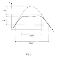
- the gain curve of the active zone alone represented by the dot-dash line has a first bandwidth OBW1
- the gain curve of the amplifier with a waveguide represented by the continuous line has a second bandwidth OBW2, substantially greater than OBW1.
- Optimization of the gain curve by introducing a photonic crystal in the vicinity of the active zone may be accomplished by computer simulation.
- F2P photonic devices
- the holes 5 have substantially a cylindrical shape, the axes of the cylinders being mutually parallel and perpendicular to the mid-plane of the stripe of the active zone. In the figures, the axes of the holes are parallel to the (O, Z) direction.
- the main characteristics of the waveguide are essentially the geometrical parameters of the holes constituting the waveguide and their distribution.
- the holes have a diameter of about 100 nanometres and a depth of 3 microns.
- the distribution of the holes also allows the attenuation introduced by the waveguide to be modulated.
- Figures 4, 5 and 6 show three possible distributions of holes, again in top view.
- the density of holes 5 on either side of the active zone is substantially uniform.
- the density of holes 5 in each structure varies continuously in a direction OX parallel to that of the stripe.
- the density of holes 5 in each structure varies continuously in a direction OY perpendicular to that of the stripe of the active zone.
- OX parallel to that of the stripe
- OY perpendicular to that of the stripe of the active zone.
- Figures 7 to 11 show, seen in cross section in the (O,Y,Z) plane, the various steps of the process for producing an optical amplifier according to the invention, the cross sections on the left-hand side being carried out away from the photonic-crystal zone, and the cross sections on the right-hand side being carried out in the centre of the photonic-crystal zone.
Landscapes
- Physics & Mathematics (AREA)
- Condensed Matter Physics & Semiconductors (AREA)
- General Physics & Mathematics (AREA)
- Electromagnetism (AREA)
- Optics & Photonics (AREA)
- Semiconductor Lasers (AREA)
- Optical Integrated Circuits (AREA)
Abstract
Description
- The field of the invention is that of optical amplifiers for fibre-optic devices used especially in optical telecommunications.
- Optical amplification, which has been around for some twenty years, has many advantages over conventional systems composed of optoelectronic repeaters-regenerators, in particular in WDM (wavelength division multiplexing) systems. In these WDM systems, the optical amplifiers are used for simultaneously amplifying several signals at different wavelengths.
- Optical amplification is based on the phenomenon of stimulated emission. The signal is amplified in a waveguide thanks to an external injection of energy, called pumping, which creates a population inversion within the amplifying medium. The incident photons on passing through the amplifying medium give rise to photons of the same frequency, the same phase and the same direction.
- At the present time, there are two broad types of optical amplifiers. These are, on the one hand, erbium-doped fibre amplifiers better known as EDFAs and, on the other hand, semiconductor amplifiers better known as SOAs. In the case of EDFAs, the pumping is optical pumping provided by a pump laser, while in the case of SOAs, the pumping is of electronic origin, an electrical pump current creating the population inversion in an active zone.
- One of the important parameters of an amplifier is the spectral width of its gain curve. This width is better known as OBW (optical bandwidth). It is conventionally defined as the spectral width corresponding to the wavelength range in which the gain is greater than half the maximum gain, as indicated in Figure 1 which shows the variation A in gain as a function of the optical wavelength λ. When optical amplifiers are used in WDM devices, the optical bandwidth OBW is a fundamental parameter. This is because, since the various transmission channels are separated by a certain spectral width imposed by the optical transmission standards, the OBW will determine the maximum number of channels that can be amplified. The distance separating two channels may be up to 20 nanometres in a "coarse" WDM base configuration. Thus, to amplify eight channels corresponding to the S-C-L optical telecommunication bands, a 140 nanometre OBW is necessary.
- Now, the bandwidth of an EDFA amplifier does not exceed 40 nanometres and the bandwidth of an amplifier of standard SOA type does not exceed 80 nanometres. Consequently, in the best case, two SOA amplifiers are needed to amplify all of the eight channels used, each of the two amplifiers being dedicated to one part of the bandwidth. This solution is necessarily complex to implement and incurs a substantial additional cost.
- The object of the invention is to increase the bandwidth of an SOA amplifier so that a larger number of channels can be amplified simultaneously. The basis of the invention is the addition to the amplifier of an element that induces moderate losses in the maximum gain zone so as to enlarge the bandwidth of the gain curve.
- More precisely, the subject of the invention is a semiconductor optical amplifier possessing an active zone, said active zone having an initial gain curve dependent on the wavelength and possessing a first bandwidth, characterized in that said amplifier includes, in the vicinity of said active zone, an electrically tuneable photonic-crystal waveguide, said waveguide being dimensioned and tuned so that the final gain curve of the optical amplifier has a second bandwidth greater than the first bandwidth.
- Advantageously, since the active zone has substantially the form of a thin elongate straight stripe, the photonic-crystal waveguide consists of two identical structures placed symmetrically on either side of said stripe.
- Advantageously, each structure comprises essentially a plurality of holes of substantially cylindrical shape, the axes of the cylinders being mutually parallel and perpendicular to the mid-plane of the stripe of the active zone.
- Advantageously, the stripe has a length of about one millimetre and the structure has a width of a few tens of microns in the direction of the stripe, the holes have a mean diameter of around one hundred nanometres and a mean depth of three microns and the distance separating a hole from its immediate neighbour is a few hundred nanometres.
- Advantageously, the density of holes in each structure is substantially uniform.
- Advantageously, the density of holes in each structure varies continuously in a direction parallel to that of the stripe or in a direction perpendicular to that of the stripe.
- The invention also relates to a process for producing a semiconductor optical amplifier according to the invention, characterized in that it comprises at least the following production steps:
- 1 st step: production of the active zone under the upper face of a substrate - there are a number of techniques known to those skilled in the art which allow this step to be carried out;
- 2nd step: deposition of a protective layer on said upper face of said substrate away from unprotected zones corresponding to the implantation of the future holes constituting the photonic-crystal waveguide, the deposition being carried out by resist deposition, masking and exposure by electron beams;
- 3rd step: etching of the holes in the unprotected zones; and
- 4th step: implantation of the control electrodes.
- The invention will be more clearly understood and other advantages will become apparent on reading the following description given by way of non-limiting example and thanks to the appended figures in which:
- Figure 1 shows the variation of the gain curve as a function of the wavelength in a semiconductor optical amplifier according to the prior art;
- Figure 2 shows a view from above of an optical amplifier according to the invention;
- Figure 3 shows the variation of the gain curve as a function of the wavelength in a semiconductor optical amplifier according to the invention;
- Figures 4 to 6 show various configurations of the photonic-crystal waveguide structure according to the invention; and
- Figures 7 to 11 show, seen in cross section, the various steps of the process for producing an optical amplifier according to the invention, the cross sections on the left of the figures being away from the photonic-crystal zone, while the cross sections on the right of the figures are carried out at the centre of the photonic-crystal zone.
- Conventionally, a photonic amplifier comprises an active zone produced in a substrate. Said zone generally has the shape of a straight stripe. It is produced in a material having a high index relative to that of the substrate so as to ensure guided propagation of the optical waves. Its length is of the order of one millimetre, its width is a few microns and its thickness is a few hundred nanometres. Electrodes provide the injection of pump current into the active zone so as to ensure the population inversion needed to amplify an optical signal passing through the active zone. As indicated in Figure 1, the amplification gain depends on the wavelength. It passes through a maximum and, as mentioned, has a spectral width called OBW.
- In an amplifier according to the invention as shown in the top view of Figure 2, the
amplifier 1 includes, in the vicinity of theactive zone 2, an electrically tuneable photonic-crystal waveguide 3. To make it easier to examine the figures representing the amplifier or the waveguide, all the figures are drawn in the same reference frame (O,X,Y,Z). Thus, the top view shown in Figure 2 is in the (O,X,Y) plane. This photonic-crystal waveguide 3 consists of twoidentical structures 4 symmetrically placed on either side of the stripe of theactive zone 2. - Photonic crystals are periodic structures designed to modify the propagation of electromagnetic waves. Since the underlying physical phenomenon is the diffraction of light by the microstructure, the periodicity of the crystal must be of the order of one half of the wavelength of the incident light in order to generate interference patterns, i.e. between 400 and 600 nanometres for operating in the near infrared. These structures are presently being used in many experiments in optics, such as spontaneous emission inhibition, high-reflectivity omnidirectional mirrors, low-loss waveguides, etc. Photonic crystals already allow light to be controlled and manipulated for the purpose of telecommunication-type applications. These crystals have in fact reached the level of maturity needed for developing industrial applications.
- For the desired application, the waveguide structures essentially consist of a plurality of regularly deposited micro-holes 5. The waveguide therefore has the property of attenuating the optical signal passing through the active zone. This attenuation, which is dependent on the wavelength, is created by the coupling between the fundamental mode and a counterpropagating higher-order mode. It passes through a maximum for a given wavelength. This maximum may be controlled by injecting a current through the waveguide by means of electrodes. The attenuation also depends on the physical characteristics of the waveguide. Thus, by varying both the current flowing through the waveguide and its physical characteristics, it is possible to attenuate the initial curve of the active zone in its maximum gain region in order to obtain a gain curve having a "plateau" in which the variations, as a function of the wavelength, are small. Thus, the OBW of the amplifying medium is enlarged, which is the desired objective.
- Thus, in Figure 3, the gain curve of the active zone alone represented by the dot-dash line has a first bandwidth OBW1, while the gain curve of the amplifier with a waveguide represented by the continuous line has a second bandwidth OBW2, substantially greater than OBW1. Optimization of the gain curve by introducing a photonic crystal in the vicinity of the active zone may be accomplished by computer simulation. For this purpose, it is possible to use the "Fdtd 2d simulator for photonic devices (F2P)" simulation software developed by Min Qiu of the Royal Institute of Technology of Sweden (or KTH).
- The
holes 5 have substantially a cylindrical shape, the axes of the cylinders being mutually parallel and perpendicular to the mid-plane of the stripe of the active zone. In the figures, the axes of the holes are parallel to the (O, Z) direction. - The main characteristics of the waveguide are essentially the geometrical parameters of the holes constituting the waveguide and their distribution. In general, the holes have a diameter of about 100 nanometres and a depth of 3 microns. The distribution of the holes also allows the attenuation introduced by the waveguide to be modulated. As non-limiting examples, Figures 4, 5 and 6 show three possible distributions of holes, again in top view. In Figure 4, the density of
holes 5 on either side of the active zone is substantially uniform. In Figure 5, the density ofholes 5 in each structure varies continuously in a direction OX parallel to that of the stripe. In Figure 6, the density ofholes 5 in each structure varies continuously in a direction OY perpendicular to that of the stripe of the active zone. Of course, other distributions are possible. - The technical production of a semiconductor optical amplifier poses no particular problems. As an example, Figures 7 to 11 show, seen in cross section in the (O,Y,Z) plane, the various steps of the process for producing an optical amplifier according to the invention, the cross sections on the left-hand side being carried out away from the photonic-crystal zone, and the cross sections on the right-hand side being carried out in the centre of the photonic-crystal zone.
- In these figures, the four main production steps are shown:
-
Step 1 shown in Figures 7 and 8: production of the active zone 2:- production of the
layer 20 constituting the active structure on asubstrate 10, this layer being common to the photonic-crystal zone; - production of the mesa constituting the
active zone 2 by etching the layer constituting the active structure followed by filling-in of the mesa; and - production of an upper layer on top of the buried active zone;
- production of the
-
Step 2 shown in Figure 9: production of the imprint for the photonic waveguide:- deposition of a protective resist
layer 30 on the upper layer; - masking of the zones located away from the waveguide; and
- exposure of the resist layer, for example by e-beam lithography, making it possible to eliminate the protective resist at the location of the future holes 50 constituting the photonic waveguide;
- deposition of a protective resist
-
Step 3 shown in Figure 10: production of the waveguide:- Etching of the
holes 5 constituting the photonic waveguide; and - cleaning of the protective resist; and
- Etching of the
-
Step 4 shown in Figure 11: finishing:- metallization of the
zones 40 corresponding to the electrodes for controlling the active zone and the waveguide.
- metallization of the
Claims (8)
- Semiconductor optical amplifier (1) possessing an active zone (2), said active zone having an initial gain curve dependent on the wavelength and possessing a first bandwidth (OBW1), characterized in that said amplifier (1) includes, in the vicinity of said active zone, an electrically tuneable photonic-crystal waveguide, said waveguide being dimensioned and tuned so that the final gain curve of the optical amplifier has a second bandwidth (OBW2) greater than the first bandwidth (OBW1).
- Optical amplifier according to Claim 1, characterized in that since the active zone (2) has substantially the form of a thin elongate straight stripe, the photonic-crystal waveguide consists of two identical structures (4) placed symmetrically on either side of said stripe.
- Optical amplifier according to Claim 2, characterized in that each structure (4) comprises essentially a plurality of holes (5) of substantially cylindrical shape, the axes of the cylinders being mutually parallel and perpendicular to the mid-plane of the stripe of the active zone (2).
- Optical amplifier according to Claim 3, characterized in that the stripe of the active zone has a length of about one millimetre and each structure (4) has a width of a few tens of microns in the direction of the stripe, in that the holes (5) have a mean diameter of around 100 nanometres and a mean depth of 3 microns and in that the distance separating a hole from its immediate neighbour is a few hundred nanometres.
- Optical amplifier according to Claim 3, characterized in that the density of holes (5) in each structure is substantially uniform.
- Optical amplifier according to Claim 3, characterized in that the density of holes (5) in each structure (4) varies continuously in a direction parallel to that of the stripe.
- Optical amplifier according to Claim 3, characterized in that the density of holes (5) in each structure (4) varies continuously in a direction perpendicular to that of the stripe.
- Process for producing a semiconductor optical amplifier according to one of the preceding claims, characterized in that it comprises at least the following production steps:• 1 st step: production of the active zone (2) on the upper face of a substrate (10);• 2nd step: deposition of a protective layer (30) on said upper face of said substrate away from unprotected zones corresponding to the implantation of the future holes constituting the photonic-crystal waveguide, the deposition being carried out by resist deposition, masking and exposure by electron beams;• 3rd step: etching of the holes (5) in the unprotected zones; and• 4th step: implantation of the control electrodes.
Applications Claiming Priority (1)
| Application Number | Priority Date | Filing Date | Title |
|---|---|---|---|
| FR0607393A FR2905036B1 (en) | 2006-08-18 | 2006-08-18 | OPTICAL AMPLIFIER WITH SEMI-CONDUCTOR WITH ENLARGED BANDWIDTH. |
Publications (2)
| Publication Number | Publication Date |
|---|---|
| EP1890366A1 true EP1890366A1 (en) | 2008-02-20 |
| EP1890366B1 EP1890366B1 (en) | 2015-03-18 |
Family
ID=37946743
Family Applications (1)
| Application Number | Title | Priority Date | Filing Date |
|---|---|---|---|
| EP07113763.2A Not-in-force EP1890366B1 (en) | 2006-08-18 | 2007-08-03 | Semiconductor optical amplifier with enlarged bandwith |
Country Status (2)
| Country | Link |
|---|---|
| EP (1) | EP1890366B1 (en) |
| FR (1) | FR2905036B1 (en) |
Citations (4)
| Publication number | Priority date | Publication date | Assignee | Title |
|---|---|---|---|---|
| EP0450603A2 (en) * | 1990-04-03 | 1991-10-09 | Canon Kabushiki Kaisha | Method and apparatus for light amplification exhibiting a flat gain spectrum |
| JP2000114670A (en) * | 1998-10-08 | 2000-04-21 | Hitachi Cable Ltd | Wideband semiconductor optical amplifier |
| US6671086B1 (en) * | 2002-02-19 | 2003-12-30 | Finisar Corporation | Semiconductor optical amplifiers with broadened gain spectrum |
| US7079309B1 (en) * | 2003-06-25 | 2006-07-18 | Sandia Corporation | Use of a photonic crystal for optical amplifier gain control |
-
2006
- 2006-08-18 FR FR0607393A patent/FR2905036B1/en active Active
-
2007
- 2007-08-03 EP EP07113763.2A patent/EP1890366B1/en not_active Not-in-force
Patent Citations (4)
| Publication number | Priority date | Publication date | Assignee | Title |
|---|---|---|---|---|
| EP0450603A2 (en) * | 1990-04-03 | 1991-10-09 | Canon Kabushiki Kaisha | Method and apparatus for light amplification exhibiting a flat gain spectrum |
| JP2000114670A (en) * | 1998-10-08 | 2000-04-21 | Hitachi Cable Ltd | Wideband semiconductor optical amplifier |
| US6671086B1 (en) * | 2002-02-19 | 2003-12-30 | Finisar Corporation | Semiconductor optical amplifiers with broadened gain spectrum |
| US7079309B1 (en) * | 2003-06-25 | 2006-07-18 | Sandia Corporation | Use of a photonic crystal for optical amplifier gain control |
Non-Patent Citations (1)
| Title |
|---|
| JAPANESE JOURNAL OF APPLIED PHYSICS, PART 1 (REGULAR PAPERS, SHORT NOTES & REVIEW PAPERS) JAPAN SOC. APPL. PHYS JAPAN, vol. 45, no. 8A, 4 August 2006 (2006-08-04), pages 6116 - 6120, XP002431044, ISSN: 0021-4922 * |
Also Published As
| Publication number | Publication date |
|---|---|
| FR2905036B1 (en) | 2008-10-24 |
| EP1890366B1 (en) | 2015-03-18 |
| FR2905036A1 (en) | 2008-02-22 |
Similar Documents
| Publication | Publication Date | Title |
|---|---|---|
| JP3243123B2 (en) | Optical filter device | |
| Sugimoto et al. | Fabrication and characterization of different types of two-dimensional AlGaAs photonic crystal slabs | |
| US7440658B2 (en) | Photonic crystal coupling defect waveguide | |
| US7831124B2 (en) | Photonic crystal optical device | |
| KR20040073317A (en) | Two-dimensional photonic crystal cavity and channel add/drop filter | |
| CA2728879A1 (en) | Composite subwavelength-structured waveguide in optical systems | |
| AU4339393A (en) | Filter with preselected attenuation/wavelength characteristic | |
| EP0897124A1 (en) | Design of complex optical fiber filters using long-period gratings | |
| US7981707B2 (en) | Method for enhancing optical characteristics of multilayer optoelectronic components | |
| CA2385364A1 (en) | Multi-wavelength laser system | |
| EP1890366B1 (en) | Semiconductor optical amplifier with enlarged bandwith | |
| Winick | Design of grating-assisted waveguide couplers with weighted coupling | |
| KR100445824B1 (en) | Method for fabricating optical loss filter and optical loss filter | |
| JPH03110884A (en) | Distributed feedback semiconductor laser and manufacture thereof | |
| GB2379084A (en) | Surface emitting laser | |
| JP3921987B2 (en) | Photonic crystal waveguide and manufacturing method thereof | |
| US7224868B2 (en) | Radiation-free optical cavity | |
| Beaurain et al. | Characterization and fabrication of InGaAsP/InP deep‐etched micro‐waveguides | |
| Shi et al. | Improved single-mode property of DFB semiconductor laser based on sampling technique using chirp compensation | |
| WO2006084063A2 (en) | A semiconductor optical amplifier having a non-uniform injection current density | |
| GB2637144A (en) | Coupled laser array | |
| KR100818448B1 (en) | Control method of semiconductor laser, optical component, laser device and semiconductor laser | |
| JP2005260005A (en) | Optical amplifier and optical amplification device | |
| KR20020044603A (en) | Multi-wavelength semiconductor laser array and method for fabricating the same | |
| Kim et al. | Waveguide beamsplitters integrated with an erbium-doped thin-film optical amplifier |
Legal Events
| Date | Code | Title | Description |
|---|---|---|---|
| PUAI | Public reference made under article 153(3) epc to a published international application that has entered the european phase |
Free format text: ORIGINAL CODE: 0009012 |
|
| AK | Designated contracting states |
Kind code of ref document: A1 Designated state(s): AT BE BG CH CY CZ DE DK EE ES FI FR GB GR HU IE IS IT LI LT LU LV MC MT NL PL PT RO SE SI SK TR |
|
| AX | Request for extension of the european patent |
Extension state: AL BA HR MK YU |
|
| 17P | Request for examination filed |
Effective date: 20080620 |
|
| AKX | Designation fees paid |
Designated state(s): AT BE BG CH CY CZ DE DK EE ES FI FR GB GR HU IE IS IT LI LT LU LV MC MT NL PL PT RO SE SI SK TR |
|
| RAP1 | Party data changed (applicant data changed or rights of an application transferred) |
Owner name: ALCATEL LUCENT |
|
| 111Z | Information provided on other rights and legal means of execution |
Free format text: AT BE BG CH CY CZ DE DK EE ES FI FR GB GR HU IE IS IT LI LT LU LV MC MT NL PL PT RO SE SI SK TR Effective date: 20130410 |
|
| RAP1 | Party data changed (applicant data changed or rights of an application transferred) |
Owner name: ALCATEL LUCENT |
|
| GRAP | Despatch of communication of intention to grant a patent |
Free format text: ORIGINAL CODE: EPIDOSNIGR1 |
|
| INTG | Intention to grant announced |
Effective date: 20141016 |
|
| D11X | Information provided on other rights and legal means of execution (deleted) | ||
| GRAS | Grant fee paid |
Free format text: ORIGINAL CODE: EPIDOSNIGR3 |
|
| GRAA | (expected) grant |
Free format text: ORIGINAL CODE: 0009210 |
|
| AK | Designated contracting states |
Kind code of ref document: B1 Designated state(s): AT BE BG CH CY CZ DE DK EE ES FI FR GB GR HU IE IS IT LI LT LU LV MC MT NL PL PT RO SE SI SK TR |
|
| REG | Reference to a national code |
Ref country code: GB Ref legal event code: FG4D |
|
| REG | Reference to a national code |
Ref country code: CH Ref legal event code: EP |
|
| REG | Reference to a national code |
Ref country code: IE Ref legal event code: FG4D |
|
| REG | Reference to a national code |
Ref country code: AT Ref legal event code: REF Ref document number: 717101 Country of ref document: AT Kind code of ref document: T Effective date: 20150415 |
|
| REG | Reference to a national code |
Ref country code: DE Ref legal event code: R096 Ref document number: 602007040650 Country of ref document: DE Effective date: 20150430 |
|
| REG | Reference to a national code |
Ref country code: NL Ref legal event code: VDEP Effective date: 20150318 |
|
| REG | Reference to a national code |
Ref country code: NL Ref legal event code: VDEP Effective date: 20150318 |
|
| PG25 | Lapsed in a contracting state [announced via postgrant information from national office to epo] |
Ref country code: SE Free format text: LAPSE BECAUSE OF FAILURE TO SUBMIT A TRANSLATION OF THE DESCRIPTION OR TO PAY THE FEE WITHIN THE PRESCRIBED TIME-LIMIT Effective date: 20150318 Ref country code: LT Free format text: LAPSE BECAUSE OF FAILURE TO SUBMIT A TRANSLATION OF THE DESCRIPTION OR TO PAY THE FEE WITHIN THE PRESCRIBED TIME-LIMIT Effective date: 20150318 Ref country code: FI Free format text: LAPSE BECAUSE OF FAILURE TO SUBMIT A TRANSLATION OF THE DESCRIPTION OR TO PAY THE FEE WITHIN THE PRESCRIBED TIME-LIMIT Effective date: 20150318 |
|
| REG | Reference to a national code |
Ref country code: AT Ref legal event code: MK05 Ref document number: 717101 Country of ref document: AT Kind code of ref document: T Effective date: 20150318 |
|
| REG | Reference to a national code |
Ref country code: FR Ref legal event code: PLFP Year of fee payment: 9 |
|
| REG | Reference to a national code |
Ref country code: LT Ref legal event code: MG4D |
|
| PG25 | Lapsed in a contracting state [announced via postgrant information from national office to epo] |
Ref country code: LV Free format text: LAPSE BECAUSE OF FAILURE TO SUBMIT A TRANSLATION OF THE DESCRIPTION OR TO PAY THE FEE WITHIN THE PRESCRIBED TIME-LIMIT Effective date: 20150318 Ref country code: GR Free format text: LAPSE BECAUSE OF FAILURE TO SUBMIT A TRANSLATION OF THE DESCRIPTION OR TO PAY THE FEE WITHIN THE PRESCRIBED TIME-LIMIT Effective date: 20150619 |
|
| PG25 | Lapsed in a contracting state [announced via postgrant information from national office to epo] |
Ref country code: NL Free format text: LAPSE BECAUSE OF FAILURE TO SUBMIT A TRANSLATION OF THE DESCRIPTION OR TO PAY THE FEE WITHIN THE PRESCRIBED TIME-LIMIT Effective date: 20150318 |
|
| PG25 | Lapsed in a contracting state [announced via postgrant information from national office to epo] |
Ref country code: RO Free format text: LAPSE BECAUSE OF FAILURE TO SUBMIT A TRANSLATION OF THE DESCRIPTION OR TO PAY THE FEE WITHIN THE PRESCRIBED TIME-LIMIT Effective date: 20150318 Ref country code: EE Free format text: LAPSE BECAUSE OF FAILURE TO SUBMIT A TRANSLATION OF THE DESCRIPTION OR TO PAY THE FEE WITHIN THE PRESCRIBED TIME-LIMIT Effective date: 20150318 Ref country code: CZ Free format text: LAPSE BECAUSE OF FAILURE TO SUBMIT A TRANSLATION OF THE DESCRIPTION OR TO PAY THE FEE WITHIN THE PRESCRIBED TIME-LIMIT Effective date: 20150318 Ref country code: PT Free format text: LAPSE BECAUSE OF FAILURE TO SUBMIT A TRANSLATION OF THE DESCRIPTION OR TO PAY THE FEE WITHIN THE PRESCRIBED TIME-LIMIT Effective date: 20150720 Ref country code: SK Free format text: LAPSE BECAUSE OF FAILURE TO SUBMIT A TRANSLATION OF THE DESCRIPTION OR TO PAY THE FEE WITHIN THE PRESCRIBED TIME-LIMIT Effective date: 20150318 Ref country code: ES Free format text: LAPSE BECAUSE OF FAILURE TO SUBMIT A TRANSLATION OF THE DESCRIPTION OR TO PAY THE FEE WITHIN THE PRESCRIBED TIME-LIMIT Effective date: 20150318 |
|
| PG25 | Lapsed in a contracting state [announced via postgrant information from national office to epo] |
Ref country code: IS Free format text: LAPSE BECAUSE OF FAILURE TO SUBMIT A TRANSLATION OF THE DESCRIPTION OR TO PAY THE FEE WITHIN THE PRESCRIBED TIME-LIMIT Effective date: 20150718 Ref country code: AT Free format text: LAPSE BECAUSE OF FAILURE TO SUBMIT A TRANSLATION OF THE DESCRIPTION OR TO PAY THE FEE WITHIN THE PRESCRIBED TIME-LIMIT Effective date: 20150318 Ref country code: PL Free format text: LAPSE BECAUSE OF FAILURE TO SUBMIT A TRANSLATION OF THE DESCRIPTION OR TO PAY THE FEE WITHIN THE PRESCRIBED TIME-LIMIT Effective date: 20150318 |
|
| REG | Reference to a national code |
Ref country code: DE Ref legal event code: R097 Ref document number: 602007040650 Country of ref document: DE |
|
| PG25 | Lapsed in a contracting state [announced via postgrant information from national office to epo] |
Ref country code: IT Free format text: LAPSE BECAUSE OF FAILURE TO SUBMIT A TRANSLATION OF THE DESCRIPTION OR TO PAY THE FEE WITHIN THE PRESCRIBED TIME-LIMIT Effective date: 20150318 |
|
| PLBE | No opposition filed within time limit |
Free format text: ORIGINAL CODE: 0009261 |
|
| STAA | Information on the status of an ep patent application or granted ep patent |
Free format text: STATUS: NO OPPOSITION FILED WITHIN TIME LIMIT |
|
| PG25 | Lapsed in a contracting state [announced via postgrant information from national office to epo] |
Ref country code: DK Free format text: LAPSE BECAUSE OF FAILURE TO SUBMIT A TRANSLATION OF THE DESCRIPTION OR TO PAY THE FEE WITHIN THE PRESCRIBED TIME-LIMIT Effective date: 20150318 |
|
| 26N | No opposition filed |
Effective date: 20151221 |
|
| PG25 | Lapsed in a contracting state [announced via postgrant information from national office to epo] |
Ref country code: SI Free format text: LAPSE BECAUSE OF FAILURE TO SUBMIT A TRANSLATION OF THE DESCRIPTION OR TO PAY THE FEE WITHIN THE PRESCRIBED TIME-LIMIT Effective date: 20150318 |
|
| PG25 | Lapsed in a contracting state [announced via postgrant information from national office to epo] |
Ref country code: MC Free format text: LAPSE BECAUSE OF FAILURE TO SUBMIT A TRANSLATION OF THE DESCRIPTION OR TO PAY THE FEE WITHIN THE PRESCRIBED TIME-LIMIT Effective date: 20150318 Ref country code: LU Free format text: LAPSE BECAUSE OF FAILURE TO SUBMIT A TRANSLATION OF THE DESCRIPTION OR TO PAY THE FEE WITHIN THE PRESCRIBED TIME-LIMIT Effective date: 20150803 |
|
| REG | Reference to a national code |
Ref country code: CH Ref legal event code: PL |
|
| PG25 | Lapsed in a contracting state [announced via postgrant information from national office to epo] |
Ref country code: CH Free format text: LAPSE BECAUSE OF NON-PAYMENT OF DUE FEES Effective date: 20150831 Ref country code: LI Free format text: LAPSE BECAUSE OF NON-PAYMENT OF DUE FEES Effective date: 20150831 |
|
| REG | Reference to a national code |
Ref country code: IE Ref legal event code: MM4A |
|
| PG25 | Lapsed in a contracting state [announced via postgrant information from national office to epo] |
Ref country code: IE Free format text: LAPSE BECAUSE OF NON-PAYMENT OF DUE FEES Effective date: 20150803 |
|
| REG | Reference to a national code |
Ref country code: FR Ref legal event code: PLFP Year of fee payment: 10 |
|
| PG25 | Lapsed in a contracting state [announced via postgrant information from national office to epo] |
Ref country code: BE Free format text: LAPSE BECAUSE OF FAILURE TO SUBMIT A TRANSLATION OF THE DESCRIPTION OR TO PAY THE FEE WITHIN THE PRESCRIBED TIME-LIMIT Effective date: 20150318 |
|
| PG25 | Lapsed in a contracting state [announced via postgrant information from national office to epo] |
Ref country code: MT Free format text: LAPSE BECAUSE OF FAILURE TO SUBMIT A TRANSLATION OF THE DESCRIPTION OR TO PAY THE FEE WITHIN THE PRESCRIBED TIME-LIMIT Effective date: 20150318 |
|
| PG25 | Lapsed in a contracting state [announced via postgrant information from national office to epo] |
Ref country code: BG Free format text: LAPSE BECAUSE OF FAILURE TO SUBMIT A TRANSLATION OF THE DESCRIPTION OR TO PAY THE FEE WITHIN THE PRESCRIBED TIME-LIMIT Effective date: 20150318 Ref country code: HU Free format text: LAPSE BECAUSE OF FAILURE TO SUBMIT A TRANSLATION OF THE DESCRIPTION OR TO PAY THE FEE WITHIN THE PRESCRIBED TIME-LIMIT; INVALID AB INITIO Effective date: 20070803 |
|
| PG25 | Lapsed in a contracting state [announced via postgrant information from national office to epo] |
Ref country code: CY Free format text: LAPSE BECAUSE OF FAILURE TO SUBMIT A TRANSLATION OF THE DESCRIPTION OR TO PAY THE FEE WITHIN THE PRESCRIBED TIME-LIMIT Effective date: 20150318 |
|
| REG | Reference to a national code |
Ref country code: FR Ref legal event code: PLFP Year of fee payment: 11 |
|
| PG25 | Lapsed in a contracting state [announced via postgrant information from national office to epo] |
Ref country code: TR Free format text: LAPSE BECAUSE OF FAILURE TO SUBMIT A TRANSLATION OF THE DESCRIPTION OR TO PAY THE FEE WITHIN THE PRESCRIBED TIME-LIMIT Effective date: 20150318 |
|
| PGFP | Annual fee paid to national office [announced via postgrant information from national office to epo] |
Ref country code: FR Payment date: 20170822 Year of fee payment: 11 Ref country code: DE Payment date: 20170822 Year of fee payment: 11 Ref country code: GB Payment date: 20170822 Year of fee payment: 11 |
|
| REG | Reference to a national code |
Ref country code: DE Ref legal event code: R119 Ref document number: 602007040650 Country of ref document: DE |
|
| GBPC | Gb: european patent ceased through non-payment of renewal fee |
Effective date: 20180803 |
|
| REG | Reference to a national code |
Ref country code: GB Ref legal event code: 732E Free format text: REGISTERED BETWEEN 20190418 AND 20190426 |
|
| PG25 | Lapsed in a contracting state [announced via postgrant information from national office to epo] |
Ref country code: DE Free format text: LAPSE BECAUSE OF NON-PAYMENT OF DUE FEES Effective date: 20190301 |
|
| PG25 | Lapsed in a contracting state [announced via postgrant information from national office to epo] |
Ref country code: FR Free format text: LAPSE BECAUSE OF NON-PAYMENT OF DUE FEES Effective date: 20180831 |
|
| PG25 | Lapsed in a contracting state [announced via postgrant information from national office to epo] |
Ref country code: GB Free format text: LAPSE BECAUSE OF NON-PAYMENT OF DUE FEES Effective date: 20180803 |