EP1890200A2 - Electroconductive member, process cartridge, and image forming apparatus - Google Patents
Electroconductive member, process cartridge, and image forming apparatus Download PDFInfo
- Publication number
- EP1890200A2 EP1890200A2 EP07114234A EP07114234A EP1890200A2 EP 1890200 A2 EP1890200 A2 EP 1890200A2 EP 07114234 A EP07114234 A EP 07114234A EP 07114234 A EP07114234 A EP 07114234A EP 1890200 A2 EP1890200 A2 EP 1890200A2
- Authority
- EP
- European Patent Office
- Prior art keywords
- oxygen
- image
- electroconductive member
- electroconductive
- image carrier
- Prior art date
- Legal status (The legal status is an assumption and is not a legal conclusion. Google has not performed a legal analysis and makes no representation as to the accuracy of the status listed.)
- Withdrawn
Links
- 238000000034 method Methods 0.000 title claims description 42
- 239000010410 layer Substances 0.000 claims abstract description 53
- 239000002344 surface layer Substances 0.000 claims abstract description 47
- QVGXLLKOCUKJST-UHFFFAOYSA-N atomic oxygen Chemical compound [O] QVGXLLKOCUKJST-UHFFFAOYSA-N 0.000 claims abstract description 26
- 229910052760 oxygen Inorganic materials 0.000 claims abstract description 26
- 239000001301 oxygen Substances 0.000 claims abstract description 26
- -1 aluminum compound Chemical class 0.000 claims abstract description 18
- 125000004334 oxygen containing inorganic group Chemical group 0.000 claims abstract description 17
- 229910052782 aluminium Inorganic materials 0.000 claims abstract description 16
- 229910010272 inorganic material Inorganic materials 0.000 claims abstract description 15
- 239000002131 composite material Substances 0.000 claims abstract description 11
- 150000003377 silicon compounds Chemical class 0.000 claims abstract description 11
- XAGFODPZIPBFFR-UHFFFAOYSA-N aluminium Chemical compound [Al] XAGFODPZIPBFFR-UHFFFAOYSA-N 0.000 claims abstract description 7
- 229910052710 silicon Inorganic materials 0.000 claims abstract description 7
- 239000010703 silicon Substances 0.000 claims abstract description 7
- 229920005989 resin Polymers 0.000 claims description 44
- 239000011347 resin Substances 0.000 claims description 44
- VYPSYNLAJGMNEJ-UHFFFAOYSA-N Silicium dioxide Chemical compound O=[Si]=O VYPSYNLAJGMNEJ-UHFFFAOYSA-N 0.000 claims description 21
- 150000001875 compounds Chemical class 0.000 claims description 15
- 239000000377 silicon dioxide Substances 0.000 claims description 11
- 229920005992 thermoplastic resin Polymers 0.000 claims description 8
- 235000012239 silicon dioxide Nutrition 0.000 claims description 7
- 150000002500 ions Chemical class 0.000 claims description 6
- TWNQGVIAIRXVLR-UHFFFAOYSA-N oxo(oxoalumanyloxy)alumane Chemical compound O=[Al]O[Al]=O TWNQGVIAIRXVLR-UHFFFAOYSA-N 0.000 claims description 6
- 239000004020 conductor Substances 0.000 claims description 4
- 125000002887 hydroxy group Chemical group [H]O* 0.000 claims description 3
- WNROFYMDJYEPJX-UHFFFAOYSA-K aluminium hydroxide Chemical compound [OH-].[OH-].[OH-].[Al+3] WNROFYMDJYEPJX-UHFFFAOYSA-K 0.000 claims description 2
- 239000002075 main ingredient Substances 0.000 claims description 2
- 229910052914 metal silicate Inorganic materials 0.000 claims description 2
- 239000004971 Cross linker Substances 0.000 claims 1
- 241001131688 Coracias garrulus Species 0.000 description 53
- 238000012546 transfer Methods 0.000 description 46
- 238000004140 cleaning Methods 0.000 description 35
- 239000000463 material Substances 0.000 description 29
- 239000002609 medium Substances 0.000 description 29
- 239000000969 carrier Substances 0.000 description 24
- 239000002585 base Substances 0.000 description 21
- 238000000576 coating method Methods 0.000 description 18
- 239000011248 coating agent Substances 0.000 description 12
- 230000006866 deterioration Effects 0.000 description 11
- 239000000314 lubricant Substances 0.000 description 10
- 229920001228 polyisocyanate Polymers 0.000 description 10
- 239000005056 polyisocyanate Substances 0.000 description 10
- 239000000126 substance Substances 0.000 description 10
- CBENFWSGALASAD-UHFFFAOYSA-N Ozone Chemical compound [O-][O+]=O CBENFWSGALASAD-UHFFFAOYSA-N 0.000 description 9
- 230000001590 oxidative effect Effects 0.000 description 9
- 230000015572 biosynthetic process Effects 0.000 description 8
- 230000000052 comparative effect Effects 0.000 description 8
- 239000000470 constituent Substances 0.000 description 8
- 238000011156 evaluation Methods 0.000 description 8
- 239000007789 gas Substances 0.000 description 8
- HNPSIPDUKPIQMN-UHFFFAOYSA-N dioxosilane;oxo(oxoalumanyloxy)alumane Chemical compound O=[Si]=O.O=[Al]O[Al]=O HNPSIPDUKPIQMN-UHFFFAOYSA-N 0.000 description 7
- NBVXSUQYWXRMNV-UHFFFAOYSA-N fluoromethane Chemical compound FC NBVXSUQYWXRMNV-UHFFFAOYSA-N 0.000 description 7
- 229920001296 polysiloxane Polymers 0.000 description 7
- 239000007787 solid Substances 0.000 description 7
- 239000011324 bead Substances 0.000 description 6
- 239000000203 mixture Substances 0.000 description 6
- OKTJSMMVPCPJKN-UHFFFAOYSA-N Carbon Chemical compound [C] OKTJSMMVPCPJKN-UHFFFAOYSA-N 0.000 description 5
- 239000004743 Polypropylene Substances 0.000 description 5
- NIXOWILDQLNWCW-UHFFFAOYSA-N acrylic acid group Chemical group C(C=C)(=O)O NIXOWILDQLNWCW-UHFFFAOYSA-N 0.000 description 5
- 230000032683 aging Effects 0.000 description 5
- 230000002547 anomalous effect Effects 0.000 description 5
- 230000015556 catabolic process Effects 0.000 description 5
- 238000006731 degradation reaction Methods 0.000 description 5
- 239000011521 glass Substances 0.000 description 5
- 239000012948 isocyanate Substances 0.000 description 5
- 150000002513 isocyanates Chemical class 0.000 description 5
- 230000007774 longterm Effects 0.000 description 5
- 229920006146 polyetheresteramide block copolymer Polymers 0.000 description 5
- 239000004848 polyfunctional curative Substances 0.000 description 5
- 229920001155 polypropylene Polymers 0.000 description 5
- 239000004698 Polyethylene Substances 0.000 description 4
- MCMNRKCIXSYSNV-UHFFFAOYSA-N Zirconium dioxide Chemical compound O=[Zr]=O MCMNRKCIXSYSNV-UHFFFAOYSA-N 0.000 description 4
- 229920000122 acrylonitrile butadiene styrene Polymers 0.000 description 4
- 239000000654 additive Substances 0.000 description 4
- 230000000996 additive effect Effects 0.000 description 4
- 229910000323 aluminium silicate Inorganic materials 0.000 description 4
- 238000005520 cutting process Methods 0.000 description 4
- 238000000354 decomposition reaction Methods 0.000 description 4
- 230000001771 impaired effect Effects 0.000 description 4
- 238000004519 manufacturing process Methods 0.000 description 4
- 238000002156 mixing Methods 0.000 description 4
- 239000003973 paint Substances 0.000 description 4
- 229920003229 poly(methyl methacrylate) Polymers 0.000 description 4
- 229920000573 polyethylene Polymers 0.000 description 4
- 229920000642 polymer Polymers 0.000 description 4
- 239000004926 polymethyl methacrylate Substances 0.000 description 4
- URGAHOPLAPQHLN-UHFFFAOYSA-N sodium aluminosilicate Chemical compound [Na+].[Al+3].[O-][Si]([O-])=O.[O-][Si]([O-])=O URGAHOPLAPQHLN-UHFFFAOYSA-N 0.000 description 4
- JOYRKODLDBILNP-UHFFFAOYSA-N Ethyl urethane Chemical compound CCOC(N)=O JOYRKODLDBILNP-UHFFFAOYSA-N 0.000 description 3
- 229920000877 Melamine resin Polymers 0.000 description 3
- 229910021536 Zeolite Inorganic materials 0.000 description 3
- 229920001893 acrylonitrile styrene Polymers 0.000 description 3
- 229910052799 carbon Inorganic materials 0.000 description 3
- 239000003054 catalyst Substances 0.000 description 3
- 230000006835 compression Effects 0.000 description 3
- 238000007906 compression Methods 0.000 description 3
- 238000004132 cross linking Methods 0.000 description 3
- 229920001971 elastomer Polymers 0.000 description 3
- 230000005611 electricity Effects 0.000 description 3
- 239000000835 fiber Substances 0.000 description 3
- 238000004898 kneading Methods 0.000 description 3
- 238000003754 machining Methods 0.000 description 3
- 239000006249 magnetic particle Substances 0.000 description 3
- 230000000873 masking effect Effects 0.000 description 3
- 239000011159 matrix material Substances 0.000 description 3
- 229910052751 metal Inorganic materials 0.000 description 3
- 239000002184 metal Substances 0.000 description 3
- 239000002808 molecular sieve Substances 0.000 description 3
- PXHVJJICTQNCMI-UHFFFAOYSA-N nickel Substances [Ni] PXHVJJICTQNCMI-UHFFFAOYSA-N 0.000 description 3
- 230000002093 peripheral effect Effects 0.000 description 3
- 230000000704 physical effect Effects 0.000 description 3
- 229920000728 polyester Polymers 0.000 description 3
- 229920001225 polyester resin Polymers 0.000 description 3
- 239000004645 polyester resin Substances 0.000 description 3
- 229920006324 polyoxymethylene Polymers 0.000 description 3
- 229920001343 polytetrafluoroethylene Polymers 0.000 description 3
- SCUZVMOVTVSBLE-UHFFFAOYSA-N prop-2-enenitrile;styrene Chemical compound C=CC#N.C=CC1=CC=CC=C1 SCUZVMOVTVSBLE-UHFFFAOYSA-N 0.000 description 3
- 150000003839 salts Chemical class 0.000 description 3
- 238000000926 separation method Methods 0.000 description 3
- 238000001179 sorption measurement Methods 0.000 description 3
- 229920002803 thermoplastic polyurethane Polymers 0.000 description 3
- 239000010457 zeolite Substances 0.000 description 3
- GFQYVLUOOAAOGM-UHFFFAOYSA-N zirconium(iv) silicate Chemical compound [Zr+4].[O-][Si]([O-])([O-])[O-] GFQYVLUOOAAOGM-UHFFFAOYSA-N 0.000 description 3
- 239000004640 Melamine resin Substances 0.000 description 2
- 239000004793 Polystyrene Substances 0.000 description 2
- XLOMVQKBTHCTTD-UHFFFAOYSA-N Zinc monoxide Chemical compound [Zn]=O XLOMVQKBTHCTTD-UHFFFAOYSA-N 0.000 description 2
- 230000001133 acceleration Effects 0.000 description 2
- XECAHXYUAAWDEL-UHFFFAOYSA-N acrylonitrile butadiene styrene Chemical compound C=CC=C.C=CC#N.C=CC1=CC=CC=C1 XECAHXYUAAWDEL-UHFFFAOYSA-N 0.000 description 2
- 239000004676 acrylonitrile butadiene styrene Substances 0.000 description 2
- 239000006229 carbon black Substances 0.000 description 2
- 238000006243 chemical reaction Methods 0.000 description 2
- 239000003086 colorant Substances 0.000 description 2
- 238000011109 contamination Methods 0.000 description 2
- 229920001577 copolymer Polymers 0.000 description 2
- 239000006185 dispersion Substances 0.000 description 2
- 239000002612 dispersion medium Substances 0.000 description 2
- 230000005684 electric field Effects 0.000 description 2
- 238000000227 grinding Methods 0.000 description 2
- 229910052736 halogen Inorganic materials 0.000 description 2
- 150000002367 halogens Chemical class 0.000 description 2
- 239000004615 ingredient Substances 0.000 description 2
- 238000001746 injection moulding Methods 0.000 description 2
- KWGKDLIKAYFUFQ-UHFFFAOYSA-M lithium chloride Chemical compound [Li+].[Cl-] KWGKDLIKAYFUFQ-UHFFFAOYSA-M 0.000 description 2
- MHCFAGZWMAWTNR-UHFFFAOYSA-M lithium perchlorate Chemical compound [Li+].[O-]Cl(=O)(=O)=O MHCFAGZWMAWTNR-UHFFFAOYSA-M 0.000 description 2
- 229910001486 lithium perchlorate Inorganic materials 0.000 description 2
- 229920002521 macromolecule Polymers 0.000 description 2
- 238000002844 melting Methods 0.000 description 2
- 230000008018 melting Effects 0.000 description 2
- 229910044991 metal oxide Inorganic materials 0.000 description 2
- 150000004706 metal oxides Chemical class 0.000 description 2
- 238000000465 moulding Methods 0.000 description 2
- 239000002245 particle Substances 0.000 description 2
- 150000004714 phosphonium salts Chemical class 0.000 description 2
- 229920002037 poly(vinyl butyral) polymer Polymers 0.000 description 2
- 239000004417 polycarbonate Substances 0.000 description 2
- 229920000515 polycarbonate Polymers 0.000 description 2
- 239000004810 polytetrafluoroethylene Substances 0.000 description 2
- 230000002441 reversible effect Effects 0.000 description 2
- BAZAXWOYCMUHIX-UHFFFAOYSA-M sodium perchlorate Chemical compound [Na+].[O-]Cl(=O)(=O)=O BAZAXWOYCMUHIX-UHFFFAOYSA-M 0.000 description 2
- 229910001488 sodium perchlorate Inorganic materials 0.000 description 2
- 238000005507 spraying Methods 0.000 description 2
- BRKFQVAOMSWFDU-UHFFFAOYSA-M tetraphenylphosphanium;bromide Chemical compound [Br-].C1=CC=CC=C1[P+](C=1C=CC=CC=1)(C=1C=CC=CC=1)C1=CC=CC=C1 BRKFQVAOMSWFDU-UHFFFAOYSA-M 0.000 description 2
- 239000002699 waste material Substances 0.000 description 2
- XLYOFNOQVPJJNP-UHFFFAOYSA-N water Substances O XLYOFNOQVPJJNP-UHFFFAOYSA-N 0.000 description 2
- XOOUIPVCVHRTMJ-UHFFFAOYSA-L zinc stearate Chemical compound [Zn+2].CCCCCCCCCCCCCCCCCC([O-])=O.CCCCCCCCCCCCCCCCCC([O-])=O XOOUIPVCVHRTMJ-UHFFFAOYSA-L 0.000 description 2
- FKTHNVSLHLHISI-UHFFFAOYSA-N 1,2-bis(isocyanatomethyl)benzene Chemical compound O=C=NCC1=CC=CC=C1CN=C=O FKTHNVSLHLHISI-UHFFFAOYSA-N 0.000 description 1
- VZXTWGWHSMCWGA-UHFFFAOYSA-N 1,3,5-triazine-2,4-diamine Chemical compound NC1=NC=NC(N)=N1 VZXTWGWHSMCWGA-UHFFFAOYSA-N 0.000 description 1
- VZXPHDGHQXLXJC-UHFFFAOYSA-N 1,6-diisocyanato-5,6-dimethylheptane Chemical compound O=C=NC(C)(C)C(C)CCCCN=C=O VZXPHDGHQXLXJC-UHFFFAOYSA-N 0.000 description 1
- WHQOKFZWSDOTQP-UHFFFAOYSA-N 2,3-dihydroxypropyl 4-aminobenzoate Chemical compound NC1=CC=C(C(=O)OCC(O)CO)C=C1 WHQOKFZWSDOTQP-UHFFFAOYSA-N 0.000 description 1
- VZSRBBMJRBPUNF-UHFFFAOYSA-N 2-(2,3-dihydro-1H-inden-2-ylamino)-N-[3-oxo-3-(2,4,6,7-tetrahydrotriazolo[4,5-c]pyridin-5-yl)propyl]pyrimidine-5-carboxamide Chemical compound C1C(CC2=CC=CC=C12)NC1=NC=C(C=N1)C(=O)NCCC(N1CC2=C(CC1)NN=N2)=O VZSRBBMJRBPUNF-UHFFFAOYSA-N 0.000 description 1
- LDXJRKWFNNFDSA-UHFFFAOYSA-N 2-(2,4,6,7-tetrahydrotriazolo[4,5-c]pyridin-5-yl)-1-[4-[2-[[3-(trifluoromethoxy)phenyl]methylamino]pyrimidin-5-yl]piperazin-1-yl]ethanone Chemical compound C1CN(CC2=NNN=C21)CC(=O)N3CCN(CC3)C4=CN=C(N=C4)NCC5=CC(=CC=C5)OC(F)(F)F LDXJRKWFNNFDSA-UHFFFAOYSA-N 0.000 description 1
- YLZOPXRUQYQQID-UHFFFAOYSA-N 3-(2,4,6,7-tetrahydrotriazolo[4,5-c]pyridin-5-yl)-1-[4-[2-[[3-(trifluoromethoxy)phenyl]methylamino]pyrimidin-5-yl]piperazin-1-yl]propan-1-one Chemical compound N1N=NC=2CN(CCC=21)CCC(=O)N1CCN(CC1)C=1C=NC(=NC=1)NCC1=CC(=CC=C1)OC(F)(F)F YLZOPXRUQYQQID-UHFFFAOYSA-N 0.000 description 1
- UPMLOUAZCHDJJD-UHFFFAOYSA-N 4,4'-Diphenylmethane Diisocyanate Chemical compound C1=CC(N=C=O)=CC=C1CC1=CC=C(N=C=O)C=C1 UPMLOUAZCHDJJD-UHFFFAOYSA-N 0.000 description 1
- DEXFNLNNUZKHNO-UHFFFAOYSA-N 6-[3-[4-[2-(2,3-dihydro-1H-inden-2-ylamino)pyrimidin-5-yl]piperidin-1-yl]-3-oxopropyl]-3H-1,3-benzoxazol-2-one Chemical compound C1C(CC2=CC=CC=C12)NC1=NC=C(C=N1)C1CCN(CC1)C(CCC1=CC2=C(NC(O2)=O)C=C1)=O DEXFNLNNUZKHNO-UHFFFAOYSA-N 0.000 description 1
- 229910002012 Aerosil® Inorganic materials 0.000 description 1
- ZTQSAGDEMFDKMZ-UHFFFAOYSA-N Butyraldehyde Chemical compound CCCC=O ZTQSAGDEMFDKMZ-UHFFFAOYSA-N 0.000 description 1
- RYGMFSIKBFXOCR-UHFFFAOYSA-N Copper Chemical compound [Cu] RYGMFSIKBFXOCR-UHFFFAOYSA-N 0.000 description 1
- 239000005057 Hexamethylene diisocyanate Substances 0.000 description 1
- 239000006237 Intermediate SAF Substances 0.000 description 1
- 239000005058 Isophorone diisocyanate Substances 0.000 description 1
- MXRIRQGCELJRSN-UHFFFAOYSA-N O.O.O.[Al] Chemical compound O.O.O.[Al] MXRIRQGCELJRSN-UHFFFAOYSA-N 0.000 description 1
- 229930040373 Paraformaldehyde Natural products 0.000 description 1
- 229930182556 Polyacetal Natural products 0.000 description 1
- 239000004952 Polyamide Substances 0.000 description 1
- 102100040160 Rabankyrin-5 Human genes 0.000 description 1
- 101710086049 Rabankyrin-5 Proteins 0.000 description 1
- BQCADISMDOOEFD-UHFFFAOYSA-N Silver Chemical compound [Ag] BQCADISMDOOEFD-UHFFFAOYSA-N 0.000 description 1
- IWULZEHQPVDQSQ-UHFFFAOYSA-N [NH4+].[NH4+].CC([O-])=O.CCCCCCCCCCCCCCCCCC([O-])=O Chemical compound [NH4+].[NH4+].CC([O-])=O.CCCCCCCCCCCCCCCCCC([O-])=O IWULZEHQPVDQSQ-UHFFFAOYSA-N 0.000 description 1
- HHUIAYDQMNHELC-UHFFFAOYSA-N [O-2].[O-2].[O-2].[Al+3].[Al+3].O=[Si]=O Chemical compound [O-2].[O-2].[O-2].[Al+3].[Al+3].O=[Si]=O HHUIAYDQMNHELC-UHFFFAOYSA-N 0.000 description 1
- 238000005299 abrasion Methods 0.000 description 1
- 238000010521 absorption reaction Methods 0.000 description 1
- 239000006230 acetylene black Substances 0.000 description 1
- 238000013019 agitation Methods 0.000 description 1
- 229910052783 alkali metal Inorganic materials 0.000 description 1
- HSFWRNGVRCDJHI-UHFFFAOYSA-N alpha-acetylene Natural products C#C HSFWRNGVRCDJHI-UHFFFAOYSA-N 0.000 description 1
- 229920003180 amino resin Polymers 0.000 description 1
- 239000003963 antioxidant agent Substances 0.000 description 1
- 230000003078 antioxidant effect Effects 0.000 description 1
- 150000001768 cations Chemical class 0.000 description 1
- 229910052802 copper Inorganic materials 0.000 description 1
- 239000010949 copper Substances 0.000 description 1
- 239000013078 crystal Substances 0.000 description 1
- 230000002542 deteriorative effect Effects 0.000 description 1
- 238000011161 development Methods 0.000 description 1
- 230000018109 developmental process Effects 0.000 description 1
- 235000014113 dietary fatty acids Nutrition 0.000 description 1
- FSBVERYRVPGNGG-UHFFFAOYSA-N dimagnesium dioxido-bis[[oxido(oxo)silyl]oxy]silane hydrate Chemical compound O.[Mg+2].[Mg+2].[O-][Si](=O)O[Si]([O-])([O-])O[Si]([O-])=O FSBVERYRVPGNGG-UHFFFAOYSA-N 0.000 description 1
- 238000003618 dip coating Methods 0.000 description 1
- 239000002270 dispersing agent Substances 0.000 description 1
- 238000009826 distribution Methods 0.000 description 1
- HBRNMIYLJIXXEE-UHFFFAOYSA-N dodecylazanium;acetate Chemical compound CC(O)=O.CCCCCCCCCCCCN HBRNMIYLJIXXEE-UHFFFAOYSA-N 0.000 description 1
- 230000000694 effects Effects 0.000 description 1
- 239000003792 electrolyte Substances 0.000 description 1
- 230000007613 environmental effect Effects 0.000 description 1
- 238000001125 extrusion Methods 0.000 description 1
- 239000000194 fatty acid Substances 0.000 description 1
- 229930195729 fatty acid Natural products 0.000 description 1
- 150000004665 fatty acids Chemical class 0.000 description 1
- 125000000524 functional group Chemical group 0.000 description 1
- 238000007429 general method Methods 0.000 description 1
- 229910052732 germanium Inorganic materials 0.000 description 1
- GNPVGFCGXDBREM-UHFFFAOYSA-N germanium atom Chemical compound [Ge] GNPVGFCGXDBREM-UHFFFAOYSA-N 0.000 description 1
- VOZRXNHHFUQHIL-UHFFFAOYSA-N glycidyl methacrylate Chemical group CC(=C)C(=O)OCC1CO1 VOZRXNHHFUQHIL-UHFFFAOYSA-N 0.000 description 1
- 229920001927 glycidyl methacrylate-styrene-acrylonitrile Polymers 0.000 description 1
- 238000010438 heat treatment Methods 0.000 description 1
- RRAMGCGOFNQTLD-UHFFFAOYSA-N hexamethylene diisocyanate Chemical compound O=C=NCCCCCCN=C=O RRAMGCGOFNQTLD-UHFFFAOYSA-N 0.000 description 1
- 229920001903 high density polyethylene Polymers 0.000 description 1
- 239000004700 high-density polyethylene Substances 0.000 description 1
- AMGQUBHHOARCQH-UHFFFAOYSA-N indium;oxotin Chemical compound [In].[Sn]=O AMGQUBHHOARCQH-UHFFFAOYSA-N 0.000 description 1
- 239000011810 insulating material Substances 0.000 description 1
- IQPQWNKOIGAROB-UHFFFAOYSA-N isocyanate group Chemical group [N-]=C=O IQPQWNKOIGAROB-UHFFFAOYSA-N 0.000 description 1
- NIMLQBUJDJZYEJ-UHFFFAOYSA-N isophorone diisocyanate Chemical compound CC1(C)CC(N=C=O)CC(C)(CN=C=O)C1 NIMLQBUJDJZYEJ-UHFFFAOYSA-N 0.000 description 1
- 238000011068 loading method Methods 0.000 description 1
- 239000000391 magnesium silicate Substances 0.000 description 1
- 229910052919 magnesium silicate Inorganic materials 0.000 description 1
- 235000019792 magnesium silicate Nutrition 0.000 description 1
- JDSHMPZPIAZGSV-UHFFFAOYSA-N melamine Chemical compound NC1=NC(N)=NC(N)=N1 JDSHMPZPIAZGSV-UHFFFAOYSA-N 0.000 description 1
- 239000010445 mica Substances 0.000 description 1
- 229910052618 mica group Inorganic materials 0.000 description 1
- 229910052759 nickel Inorganic materials 0.000 description 1
- 239000003921 oil Substances 0.000 description 1
- 239000003960 organic solvent Substances 0.000 description 1
- 229920001197 polyacetylene Polymers 0.000 description 1
- 229920002647 polyamide Polymers 0.000 description 1
- 229920006122 polyamide resin Polymers 0.000 description 1
- 229920000767 polyaniline Polymers 0.000 description 1
- 229920000128 polypyrrole Polymers 0.000 description 1
- 239000011148 porous material Substances 0.000 description 1
- 230000002265 prevention Effects 0.000 description 1
- 238000012545 processing Methods 0.000 description 1
- 239000002296 pyrolytic carbon Substances 0.000 description 1
- 238000011084 recovery Methods 0.000 description 1
- 239000004065 semiconductor Substances 0.000 description 1
- 229920002050 silicone resin Polymers 0.000 description 1
- 229910052709 silver Inorganic materials 0.000 description 1
- 239000004332 silver Substances 0.000 description 1
- 239000000243 solution Substances 0.000 description 1
- 229910001220 stainless steel Inorganic materials 0.000 description 1
- 239000010935 stainless steel Substances 0.000 description 1
- 230000003068 static effect Effects 0.000 description 1
- 230000035882 stress Effects 0.000 description 1
- 230000003746 surface roughness Effects 0.000 description 1
- 239000000454 talc Substances 0.000 description 1
- 229910052623 talc Inorganic materials 0.000 description 1
- 238000012360 testing method Methods 0.000 description 1
- XOLBLPGZBRYERU-UHFFFAOYSA-N tin dioxide Chemical compound O=[Sn]=O XOLBLPGZBRYERU-UHFFFAOYSA-N 0.000 description 1
- 229910001887 tin oxide Inorganic materials 0.000 description 1
- DVKJHBMWWAPEIU-UHFFFAOYSA-N toluene 2,4-diisocyanate Chemical compound CC1=CC=C(N=C=O)C=C1N=C=O DVKJHBMWWAPEIU-UHFFFAOYSA-N 0.000 description 1
- 239000013638 trimer Substances 0.000 description 1
- 238000011144 upstream manufacturing Methods 0.000 description 1
- 229910052720 vanadium Inorganic materials 0.000 description 1
- 230000000007 visual effect Effects 0.000 description 1
- 239000011787 zinc oxide Substances 0.000 description 1
- 229910052845 zircon Inorganic materials 0.000 description 1
Images


Classifications
-
- G—PHYSICS
- G03—PHOTOGRAPHY; CINEMATOGRAPHY; ANALOGOUS TECHNIQUES USING WAVES OTHER THAN OPTICAL WAVES; ELECTROGRAPHY; HOLOGRAPHY
- G03G—ELECTROGRAPHY; ELECTROPHOTOGRAPHY; MAGNETOGRAPHY
- G03G15/00—Apparatus for electrographic processes using a charge pattern
- G03G15/02—Apparatus for electrographic processes using a charge pattern for laying down a uniform charge, e.g. for sensitising; Corona discharge devices
- G03G15/0208—Apparatus for electrographic processes using a charge pattern for laying down a uniform charge, e.g. for sensitising; Corona discharge devices by contact, friction or induction, e.g. liquid charging apparatus
- G03G15/0216—Apparatus for electrographic processes using a charge pattern for laying down a uniform charge, e.g. for sensitising; Corona discharge devices by contact, friction or induction, e.g. liquid charging apparatus by bringing a charging member into contact with the member to be charged, e.g. roller, brush chargers
- G03G15/0233—Structure, details of the charging member, e.g. chemical composition, surface properties
-
- G—PHYSICS
- G03—PHOTOGRAPHY; CINEMATOGRAPHY; ANALOGOUS TECHNIQUES USING WAVES OTHER THAN OPTICAL WAVES; ELECTROGRAPHY; HOLOGRAPHY
- G03G—ELECTROGRAPHY; ELECTROPHOTOGRAPHY; MAGNETOGRAPHY
- G03G15/00—Apparatus for electrographic processes using a charge pattern
- G03G15/02—Apparatus for electrographic processes using a charge pattern for laying down a uniform charge, e.g. for sensitising; Corona discharge devices
- G03G15/0208—Apparatus for electrographic processes using a charge pattern for laying down a uniform charge, e.g. for sensitising; Corona discharge devices by contact, friction or induction, e.g. liquid charging apparatus
- G03G15/025—Apparatus for electrographic processes using a charge pattern for laying down a uniform charge, e.g. for sensitising; Corona discharge devices by contact, friction or induction, e.g. liquid charging apparatus by bringing a charging member in the vicinity with the member to be charged, e.g. proximity charging, forming microgap
-
- G—PHYSICS
- G03—PHOTOGRAPHY; CINEMATOGRAPHY; ANALOGOUS TECHNIQUES USING WAVES OTHER THAN OPTICAL WAVES; ELECTROGRAPHY; HOLOGRAPHY
- G03G—ELECTROGRAPHY; ELECTROPHOTOGRAPHY; MAGNETOGRAPHY
- G03G15/00—Apparatus for electrographic processes using a charge pattern
- G03G15/06—Apparatus for electrographic processes using a charge pattern for developing
- G03G15/08—Apparatus for electrographic processes using a charge pattern for developing using a solid developer, e.g. powder developer
- G03G15/0806—Apparatus for electrographic processes using a charge pattern for developing using a solid developer, e.g. powder developer on a donor element, e.g. belt, roller
- G03G15/0818—Apparatus for electrographic processes using a charge pattern for developing using a solid developer, e.g. powder developer on a donor element, e.g. belt, roller characterised by the structure of the donor member, e.g. surface properties
-
- G—PHYSICS
- G03—PHOTOGRAPHY; CINEMATOGRAPHY; ANALOGOUS TECHNIQUES USING WAVES OTHER THAN OPTICAL WAVES; ELECTROGRAPHY; HOLOGRAPHY
- G03G—ELECTROGRAPHY; ELECTROPHOTOGRAPHY; MAGNETOGRAPHY
- G03G15/00—Apparatus for electrographic processes using a charge pattern
- G03G15/14—Apparatus for electrographic processes using a charge pattern for transferring a pattern to a second base
- G03G15/16—Apparatus for electrographic processes using a charge pattern for transferring a pattern to a second base of a toner pattern, e.g. a powder pattern, e.g. magnetic transfer
- G03G15/1665—Apparatus for electrographic processes using a charge pattern for transferring a pattern to a second base of a toner pattern, e.g. a powder pattern, e.g. magnetic transfer by introducing the second base in the nip formed by the recording member and at least one transfer member, e.g. in combination with bias or heat
- G03G15/167—Apparatus for electrographic processes using a charge pattern for transferring a pattern to a second base of a toner pattern, e.g. a powder pattern, e.g. magnetic transfer by introducing the second base in the nip formed by the recording member and at least one transfer member, e.g. in combination with bias or heat at least one of the recording member or the transfer member being rotatable during the transfer
- G03G15/1685—Structure, details of the transfer member, e.g. chemical composition
-
- G—PHYSICS
- G03—PHOTOGRAPHY; CINEMATOGRAPHY; ANALOGOUS TECHNIQUES USING WAVES OTHER THAN OPTICAL WAVES; ELECTROGRAPHY; HOLOGRAPHY
- G03G—ELECTROGRAPHY; ELECTROPHOTOGRAPHY; MAGNETOGRAPHY
- G03G2215/00—Apparatus for electrophotographic processes
- G03G2215/16—Transferring device, details
- G03G2215/1604—Main transfer electrode
- G03G2215/1614—Transfer roll
-
- Y—GENERAL TAGGING OF NEW TECHNOLOGICAL DEVELOPMENTS; GENERAL TAGGING OF CROSS-SECTIONAL TECHNOLOGIES SPANNING OVER SEVERAL SECTIONS OF THE IPC; TECHNICAL SUBJECTS COVERED BY FORMER USPC CROSS-REFERENCE ART COLLECTIONS [XRACs] AND DIGESTS
- Y10—TECHNICAL SUBJECTS COVERED BY FORMER USPC
- Y10T—TECHNICAL SUBJECTS COVERED BY FORMER US CLASSIFICATION
- Y10T428/00—Stock material or miscellaneous articles
- Y10T428/13—Hollow or container type article [e.g., tube, vase, etc.]
- Y10T428/1352—Polymer or resin containing [i.e., natural or synthetic]
- Y10T428/139—Open-ended, self-supporting conduit, cylinder, or tube-type article
-
- Y—GENERAL TAGGING OF NEW TECHNOLOGICAL DEVELOPMENTS; GENERAL TAGGING OF CROSS-SECTIONAL TECHNOLOGIES SPANNING OVER SEVERAL SECTIONS OF THE IPC; TECHNICAL SUBJECTS COVERED BY FORMER USPC CROSS-REFERENCE ART COLLECTIONS [XRACs] AND DIGESTS
- Y10—TECHNICAL SUBJECTS COVERED BY FORMER USPC
- Y10T—TECHNICAL SUBJECTS COVERED BY FORMER US CLASSIFICATION
- Y10T428/00—Stock material or miscellaneous articles
- Y10T428/13—Hollow or container type article [e.g., tube, vase, etc.]
- Y10T428/1352—Polymer or resin containing [i.e., natural or synthetic]
- Y10T428/139—Open-ended, self-supporting conduit, cylinder, or tube-type article
- Y10T428/1393—Multilayer [continuous layer]
Definitions
- the present invention relates to an electroconductive member adaptable to a charging member, a developer carrier, a transfer member, or the like disposed adjacent to an image carrier in an electrophotographic image forming apparatus such as a copying machine, a laser beam printer, or a facsimile, a process cartridge including the electroconductive member, and an image forming apparatus including the process cartridge.
- An electrophotographic image forming apparatus such as a copying machine, a laser beam printer, or a facsimile has been conventionally provided with a charging member that performs an electrification process on an image carrier (or an electrostatic latent image carrier or a photoconductor), and a transfer member that performs a transfer process on toner on the photoconductor.
- An electroconductive member is used as the charging member or the transfer member. A case using the electroconductive member as the charging member is mentioned hereinafter.
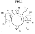
- FIG.1 is a schematic illustration of an electrophotographic image forming apparatus.
- reference numeral 11 denotes an image carrier or a photoconductor on which an electrostatic latent image is formed; 12, a charging member or a charger roller that performs an electrification process, disposed in contact with or in proximity to the image carrier 11; 13, light for exposure, such as laser light or reflected light from an original; 14, a toner carrier or a developing roller that causes toner 15 to adhere to the electrostatic latent image on the image carrier 11; 16, a transfer member (or a transfer roller) that transfers a toner image on the image carrier 11 to a recording medium 17; and 18, a cleaning member or a blade for cleaning the image carrier 11 after the transfer process.
- Reference numeral 19 denotes waste toner discharged by the cleaning member 18 removing the toner remaining on the image carrier 11; 201, a developing unit; and 211, a cleaning unit.
- the image forming apparatus as mentioned above is configured to form an image through the following processes.
- Conventional electrification methods using the charger roller include a contact electrification method that involves bringing the charger roller into contact with the image carrier.
- the conventional contact electrification method has the following problems (1) to (5).
- a proximity electrification method that involves bringing the charger roller into proximity with the image carrier, as disclosed in JPA No.3-240076 (Patent Document 1), JPA No. 2001-312121 (Patent Document 2), JPA No. 2005-91818 (Patent Document 3), and so on.
- the method electrifies the image carrier by applying a voltage to the charger roller disposed as facing the image carrier with a distance or a gap of 50 to 300 ⁇ m between when the charger roller and the image carrier are in closest proximity to each other.
- the proximity electrification method does not present the problems inherent in a contact charger unit, that is, "the adhesion of the constituent substance of the charger roller to the image carrier” and “the permanent deformation caused by the image carrier being in its stopped state for a long time.”
- the proximity electrification method is superior in electrification performance because of reducing the toner adhering to the charger roller.
- a non-contact electrification method is more excellent than the contact electrification method. Because of using corona discharge following Paschen's law between the charger roller and the image carrier to electrify the surface of the photoconductor, however, both the methods produce or generate oxidative gases such as ozone or NO x , thus leading to deterioration in the surfaces of the image carrier and the charger roller with time. The deterioration increases the likelihood of adhesion of the toner and its constituent substance to the surface of the charger roller, thus leading to the deterioration in the electrification performance of the charger roller. The deterioration results in deterioration of the electrification performance of the image carrier, or the like, thereby increasing the likelihood of image degradation.
- An object of the present invention is to provide an electroconductive member that maintains stable electrification performance and thus eliminates the occurrence of image degradation, even if it is used as a charging member over the long term.
- an electroconductive member includes an electroconductive support, an electric resistance adjusting layer formed on the electroconductive support, and a top surface layer that coats the surface of the electric resistance adjusting layer.
- the top surface layer contains at least one oxygen-containing inorganic compound selected from among a composite oxide of silicon and aluminum, an oxygen-containing silicon compound, and an oxygen-containing aluminum compound.
- FIG.2 is a schematic illustration showing a structure of a charger unit using an electroconductive member according to the embodiment of the present invention as a charging member, and the configuration of an image forming apparatus using a process cartridge.
- FIG.3 is a schematic illustration showing a structure of an image forming unit of the image forming apparatus shown in FIG.2.
- the image forming apparatus 1 includes: four image carriers (or photoconductors) 61, 61, 61 and 61 in drum form for four colors, namely, yellow (Y), magenta (M), cyan (C), and black (K), respectively, the image carriers 61 each having an image carrier layer on its surface; a charger unit 100 that substantially uniformly electrifies the image carriers 61; an exposure unit 70 that exposes the charged image carriers 61 to laser light to form electrostatic latent images on the image carriers 61; four developing units 63, 63, 63 and 63 that form toner images corresponding to the electrostatic latent images on the image carriers 61, the developing units 63 accommodating developers for the four colors, namely, yellow, magenta, cyan, and black, respectively; four primary transfer units 62, 62, 62 and 62 that transfer the toner images on the image carriers 61; an intermediate transfer unit 50 in belt form to which the toner images on the image carriers 61 are transferred; a secondary transfer unit 51 that transfers the toner images on the intermediate
- the recording media are transported one by one on a carrying roller along a traveling route from one of paper feed units 21 and 22 that accommodate the recording media to a resist roller 23, which in turn carries the recording medium to a transfer position in synchronization with the toner images on the image carriers 61.
- the exposure unit 70 of the image forming apparatus 1 irradiates the image carriers 61 electrified by the charger unit 100 with light L to form the electrostatic latent images on the image carriers 61 having photoconductivity.
- the light L is, for example, a laser light beam or the like emitted by a lamp such as a fluorescent lamp or a halogen lamp or a semiconductor device such as an LED (light emitting diode) or an LD (laser diode).
- a lamp such as a fluorescent lamp or a halogen lamp
- a semiconductor device such as an LED (light emitting diode) or an LD (laser diode).
- the LD device is used.
- the developing unit 63 has a developer carrier.
- the toner stored in the developing unit 63 is carried on a feed roller to an agitator.
- the carried toner is mixed and agitated with the developer containing a carrier that is a magnetic particle for carrying the toner to the image carrier.
- the toner is carried to a developing region facing the image carrier 61.
- the toner becomes charged during mixing and agitation, and the charged toner is transferred from the developing region to the electrostatic latent image on the image carrier 61 to develop the electrostatic latent image.
- Either a magnetic or nonmagnetic one-member developer, or a combination of both can be used as the developer, or a wet developing solution may be used as the developer.
- the primary transfer units 62 on their undersides, form an electric field of opposite polarity to the polarity of the toner to transfer the developed toner images on the image carriers 61 to the intermediate transfer unit 50.
- the primary transfer units 62 can be any of a corotron, scorotron corona transferer, a transfer roller, and a transfer brush.
- the toner images are transferred to the recording medium by the secondary transfer unit 51, in synchronization with the recording medium from the paper feed unit 22. At this point, the toner images are not first transferred to the intermediate transfer unit 50 but may be transferred directly to the recording medium.
- the fixing unit 80 applies heat and/or pressure to the toner images on the recording medium to fix the toner images on the recording medium. At this point, the fixing unit 80, during the passage of the recording medium through a pair of pressure and fixing rollers, applies heat and pressure to the recording medium to fix the toner on the recording medium, while fusing a bonding resin of the toner onto the recording medium.
- the fixing unit 80 is not in roller form but may be in belt form, or the fixing unit 80 may use a halogen lamp or the like for heat irradiation for fixing.
- the cleaning units 64 for the image carriers 61 remove the toner remaining on the image carriers 61 without being transferred to permit next image formation.
- a blade made of urethane or other rubber, a cleaning brush made of polyester or other fibers, or the like can be used as the cleaning unit 64.
- An original is first placed on an original plate of an original carrying unit 36 of a reader 30, or the original carrying unit 36 is opened to place the original on contact glass 31 and the original carrying unit 36 is closed to cover the original.
- first and second read traveling units 32 and 33 travel after the original is transported onto the contact glass 31 if the original is placed on the original carrying unit 36, or the first and second read traveling units 32 and 33 travel immediately if the original is placed on the contact glass 31.
- the first read traveling unit 32 operates in such a manner that light is emitted to the original surface from a light source provided in the first read traveling unit 32 and the light reflected from the original surface is further reflected and directed to the second read traveling unit 33.
- the second read traveling unit 33 operates in such a manner that the reflected light is reflected from a mirror through an image forming lens 34 to a CCD (charge coupled device) 35 that is a read sensor. Then, incoming light image information is read by the CCD 35 and is transmitted to a controller.
- CCD charge coupled device
- the LD or LED or the like (not shown) disposed in the exposure unit 70 of an image forming unit 60 emits laser light L2 for writing to irradiate the image carriers 61 with the laser light L2. This irradiation yields the electrostatic latent images on the surfaces of the image carriers 61.
- a paper feeder 20 operates in such a manner that the recording medium is dispensed from the multilevel paper feed cassette 21 by a paper feed roller, that the dispensed recording medium is separated by a separation roller and is delivered to a paper feed path, and that the recording medium is transported on the carrying roller to the paper feed path of the image forming unit 60.
- the image forming apparatus 1 is provided on its side with a manual paper feed tray for the manual paper feed, and a separation roller that separates the recording media, one by one, on the manual paper feed tray to direct the recording medium to a manual paper feed path for paper feeding.
- the resist roller 23 of the image forming apparatus 1 ejects only one of the recording media placed in the paper feed cassette 21, and feeds the recording medium to a secondary transfer unit located between the intermediate transfer unit 50 and the secondary transfer unit 51.
- the controller receives the image information from the reader 30, the image forming unit 60 performs laser writing and developing process as mentioned above to form the electrostatic latent images on the image carriers 61.
- the developer (or the toner and the carrier (or the magnetic particle) having the toner adhering thereto) within the developing unit 63 is drawn and held by a magnetic pole (not shown) to form a magnetic brush made of a string of magnetic particles on the developer carrier.
- the developer further acts in such a manner that the toner is transferred to the image carrier 61 through the application of a developing bias voltage to the developer carrier to make visible the electrostatic latent image on the image carrier 61, and thereby form the toner image.
- the developing bias voltage is a superposition of an alternating voltage and a direct voltage. Then, one of the paper feed rollers of the paper feeder 20 operates in order to feed the recording medium of size depending on the toner image. Moreover, a driving motor rotatably drives one of support rollers incident to the operation of the paper feed roller, and this leads to coupled rotatable driving of two other support rollers, and hence to rotatable transport of the intermediate transfer unit 50.
- the individual image forming units form mono-color images, namely, black, yellow, magenta and cyan color images, on each of the image carriers 61, by rotation of the image carriers 61.
- the mono-color images are then transferred in sequence to the intermediate transfer unit 50 to form a composite toner image on the intermediate transfer unit 50.
- the recording media are dispensed from one of the paper feed cassettes 21, and the recording media, one by one, are separated and delivered into the paper feed path by the separation roller.
- the carrying roller guides the recording medium to the paper feed path in the image forming unit 60 of the image forming apparatus 1, and strikes the recording medium against the resist roller 23 to stop the recording medium.
- the recording medium is fed into the secondary transfer unit that is an abutment between the intermediate transfer unit 50 and the secondary transfer unit 51.
- the secondary transfer unit secondarily transfers the toner image to the recording medium to record the toner image on the recording medium, by the influence of a secondary transfer bias, an abutment pressure, or the like formed in the secondary transfer unit.
- the secondary transfer bias be a direct voltage.
- the recording medium having the toner image transferred thereto is fed into the fixing unit 80 by a conveyor belt of the secondary transfer unit 51.
- the fixing unit 80 the toner image is fixed on the recording medium through the application of pressure and heat by the pressure roller. Thereafter, the recording medium is delivered onto a receiving tray 40 by a delivery roller 41.
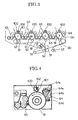
- FIG.4 is a schematic illustration showing the configuration of the charger unit using the electroconductive member according to the embodiment of the present invention as the charging member, and the configuration of the process cartridge.
- the process cartridge includes at least the image carrier 61, the charger unit 100, and the cleaning unit 64, or may further include the developing unit 63 as shown in FIG.4.
- This process cartridge in itself is detachably attached integrally to the image forming apparatus.
- the surfaces of the image carriers 61 are uniformly electrified by a charging member 101 disposed without contact with an image forming region.
- the images (or the electrostatic latent images) are formed on the surfaces of the image carriers 61 and are then made visible by the developing process to form the toner images, which in turn are transferred to the recording medium.
- the toner remaining on the image carriers 61 without being transferred to the recording medium is recovered by an auxiliary cleaning member 64d.
- a solid lubricant 64a is uniformly applied to the image carrier 61 by a coating member 64b to form a lubricant layer, in order to prevent the toner and its constituent material from adhering to the surface of the image carrier 61.
- the auxiliary cleaning member 64d can be in roller or brush form.
- Fatty acid metal salt such as zinc stearate, polytetrafluoroethylene, or the like, for example, can be used for the solid lubricant 64a.
- the solid lubricant 64a is not limited to the above but may be made of any material, provided that it can reduce a coefficient of friction on the image carrier 61 and thus impart non-adhesion to the image carrier 61.
- a blade made of silicone, urethane or other rubber, a cleaning brush made of polyester or other fibers, or the like, for example, can be used as the cleaning member 64c.
- the charger unit 100 is provided with a cleaning member 102 for removing contamination of the charging member 101.
- the cleaning member can be in roller or pad form, the cleaning member as employed in the embodiment is in roller form.
- the cleaning member 102 is fitted and rotatably and pivotally supported on a bearing disposed in a housing (not shown) of the charger unit 100.
- the cleaning member 102 abuts the charging member 101 to clean the outer periphery of the charging member 101.
- the charger unit 100 is therefore provided with the cleaning member 102 for cleaning the surface of the charging member 101.
- a brush made of polyester or other fibers, or a porous material (e.g., sponge) such as a melamine resin, for example, can be used for the cleaning member 102.
- the cleaning member 102 rotates with a differential peripheral velocity as following the rotation of the charging member 101, or the cleaning member 102 may intermittently rotate clear of the charging member 101.
- the charger unit 100 is also provided with a power supply that applies a voltage to the charging member 101.
- a direct voltage alone can be used as the voltage, it is desirable that the voltage be a superposition of a direct voltage and an alternating voltage.
- the application of the direct voltage alone to the charging member 101 can possibly result in a nonuniformity in the surface potential of the image carrier 61.
- the application of the superposed voltage to the charging member 101 leads to potential equalization of the surface of the charging member 101, thus stabilizes discharge from the charging member 101, and thus enables the surface of the image carrier 61 can become uniformly charged.
- the superposed voltage is set so that the peak-to-peak voltage of the alternating voltage is two or more times an electrification start voltage for the image carrier 61.
- the electrification start voltage refers to the absolute value of the voltage at which the image carrier 61 starts becoming charged when the direct voltage alone is applied to the charging member 101.
- the above setting leads to reverse discharge from the image carrier 61 to the charging member 101, so that the surface of the image carrier 61 can become uniformly charged with higher stability by the effect of the reverse discharge making electrification even.
- the frequency of the alternating voltage is seven or more times the peripheral velocity (or process speed) of the image carrier 61.
- the frequency is seven or more times the peripheral velocity, a moiré image becomes unrecognizable or visually unrecognizable.
- the auxiliary cleaning member 64d is configured of a brush roller, the lubricant is made of a block of zinc stearate, and the brush roller 64d that is the coating member is rotated as pressed against the lubricant by a pressurizing member such as a spring, to thereby cut away the solid lubricant from the solid lubricant block that is the lubricant and apply the solid lubricant to the image carrier 61.
- a urethane blade is used as the cleaning member and is of a counter type.
- a sponge roller made of a melamine resin is used as the cleaning member for the charging member 101.
- the cleaning member is of a type which rotates as following the rotation of the charging member, and thereby enables excellently cleaning off contamination of the surface of the charging member 101.
- FIG.5 is a schematic illustration showing the relative positions of a photoconductive layer region, an image-formation region, and a non-image-formation region of the charging member 101 that is the electroconductive member according to the embodiment of the present invention, and the image carrier 61.
- the charger unit 100 includes at least the charging member 101 disposed as facing the image carrier 61 with a minute gap G therebetween; the cleaning member 102 that cleans the charging member 101; the power supply (not shown) that applies a voltage to the charging member 101; and a pressure spring (not shown) that presses the charging member 101 against the image carrier 61 to bring the charging member 101 into contact with the image carrier 61.
- the charging member 101 is disposed as facing the image carrier 61 with the minute gap G therebetween.
- a gap holding member 103 abuts against a non-image-formation region of the charging member 101.
- the gap holding member 103 abuts against the photoconductive layer region of the image carrier 61 to thereby enable preventing variations in the gap even at the occurrence of variations in the coating thickness of the photoconductive layer.
- the gap holding members 103 are disposed on both ends of an electric resistance adjusting layer 104 formed on an electroconductive support 106. Moreover, a cap layer 105 is formed on the electric resistance adjusting layer 104 so as to prevent the toner and toner additive from adhering to the surface of the layer 104.
- the charging member 101 is not particularly limited but may be in belt, blade or plate, or semicylindrical form and be fixedly disposed. Alternatively, the charging member 101 may be in cylindrical form and be rotatably supported at both ends on gears or bearings.
- the charging member 101 When the charging member 101 is formed by a curved surface that gradually gets clear of a portion in closest proximity to the image carrier 61 upstream and downstream in the direction of movement of the image carrier 61, the surface of the image carrier 61 can become more uniformly charged. If a sharp portion is present on the surface of the charging member 101 facing the image carrier 61, a rise in the potential occurs in the portion, thus starts preferential discharge therein, and thus makes it difficult for the surface of the image carrier 61 to become uniformly charged. When the charging member 101 is of cylindrical shape and also has the curved surface, the image carrier 61 can therefore become uniformly charged.
- the discharge surface of the charging member 101 undergoes strong stress. Since the discharge occurs on the surface in the same portion at all times, deterioration is accelerated in this portion, and moreover, the degraded portion can possibly be cut away. When the charging member 101 is rotated so that its overall surface can be used for discharge, it is therefore possible to prevent the charging member 101 from deteriorating at an early stage and hence use the charging member 101 over the long term.
- the gap G between the charging member 101 and the image carrier 61 is set by the gap holding member 103 so as to be equal to or less than 100 ⁇ m or particularly lies between about 5 and 70 ⁇ m, it is possible to suppress anomalous image formation during the operation of the charger unit 100.
- the width of the gap G of 100 ⁇ m or more increases a distance which electricity produced by the charging member 101 travels until reaching the image carrier 61.
- the large gap G raises a discharge start voltage following Paschen's law. Since the large gap G further enlarges discharge space between the charging member 101 and the image carrier 61, predetermined electrification of the image carrier 61 requires discharge to yield a large amount of discharge products, and thus, the discharge products remain in the discharge space in large amounts even after image formation, adhere to the image carrier 61, and become the cause of accelerated proceeding of aging in the image carrier 61.
- the gap G of narrow width reduces the distance which the electricity produced by the charging member 101 travels until reaching the image carrier 61, and thus the image carrier 61 can become charged even if discharge energy is low.
- the narrow gap G narrows the space formed between the charging member 101 and the image carrier 61 and thus impairs a flow of air through the space.
- the discharge products formed in the discharge space remain in the discharge space in large amounts even after image formation, adhere to the image carrier 61, and become the cause of accelerated proceeding of aging in the image carrier 61, as in the case of the large gap G.
- the discharge energy is reduced to reduce the production of discharge products, and the space is such that air does not stay in the space.
- the width of the gap G is set so that the width is equal to or less than 100 ⁇ m or lies between 5 and 70 ⁇ m.
- the above toner can possibly be fused to the charging member 101 by being heated by being rubbed against the rotating image carrier 61 or charging member 101.
- the charging member 101 If the toner is fused to the charging member 101, the charging member 101 is brought close to the image carrier 61 correspondingly by the amount of the fused toner, and thus anomalous discharge occurs and causes preferential discharge in a place where the toner is fused. Desirably, therefore, the width of the gap G is set so that the width is larger than the maximum grain size of the toner for use in the image forming apparatus 1.
- the electroconductive support 106 of the charging member 101 is rotatably fitted at both ends in bearings 107 disposed on side plates of the housing (not shown) of the charger unit 100, as shown in FIG. 5.
- the bearing 107 is made of a resin having a low coefficient of friction and is pressed toward the image carrier 61 by a compression spring 108.
- a load imposed on the charging member 101 by the compression springs 108 is set, for example, at 4 to 25 N, or desirably at 6 to 15 N.
- the charging member 101 is fixedly located by being pivotally supported on the bearings 107, the width of the gap G can possibly fall outside a proper range due to vibrations during rotation of the charging member 101, offset of the charging member 101, and variations in the width of the gap G due to asperities on the surface thereof, and this results in accelerated proceeding of aging in the image carrier 61.
- the load refers to every load applied to the image carrier 61 through the gap holding member 103. Forces exerted by the compression springs 108 disposed on both ends of the charging member 101, the weight of the charging member 101 and the cleaning member 102 on their own, or the like can be used to adjust the load.
- a light load makes it impossible to suppress variations during rotation of the charging member 101 or a rebound of the driven gears or the like by impact forces.
- a heavy load leads to an increase in the friction between the charging member 101 and the fitting bearings 107 and hence to an increase in aging abrasion wear, resulting in acceleration of variations.
- the load lying between 4 and 25 N or desirably between 6 and 15 N can achieve the width of the gap G falling within the proper range, thus reduce the production of discharge products, thus reduce the amount of discharge products deposited on the image carrier 61, and thus increase the longevity of the image carrier 61. This enables preventing an anomalous spotted image or a running image from appearing.
- the gap holding member 103 is partially different in level from the electric resistance adjusting layer 104.
- a method for forming a gap between the electric resistance adjusting layer 104 and the gap holding member 103 can be accomplished by simultaneously machining the electric resistance adjusting layer 104 and the gap holding member 103 by means of machining for removal, such as cutting or grinding. The simultaneous machining makes it possible to form the gap with high precision.
- This configuration can prevent the outer surface of the end of the gap holding member 103 toward the electric resistance adjusting layer 104 from abutting the image carrier 61.
- the configuration can also prevent the occurrence of a leakage of current due to the adjacent electric resistance adjusting layer 104 coming into contact with the image carrier 61 with the above end in between.
- the end of the gap holding member 103 toward the electric resistance adjusting layer 104 is machined so as to be at lower level, the end can be used as a relief for a cutting edge or the like for the removal.
- the relief can be of any shape, provided that the shape is such that the outer surface of the end of the gap holding member 103 does not abut the image carrier 61.
- top surface layer (or cap layer) 105 of the electric resistance adjusting layer 104 When coating is used to form the top surface layer (or cap layer) 105 of the electric resistance adjusting layer 104, masking can take place in order that an unwanted area is not coated. However, it is difficult to perform control for precise masking such that the masking extends to the position of a boundary between the electric resistance adjusting layer 104 and the gap holding member 103, allowing for variations in the position of the boundary therebetween. Thus, prior to the grinding of the gap holding member 103, the top surface layer 105 is formed as extending to the end of the electric resistance adjusting layer 1.04 in contact with the gap holding member 103. This can ensure that the top surface layer 105 is formed only on the electric resistance adjusting layer 104.
- the gap holding member 103 requires the property of holding the gap G between the gap holding member 103 and the image carrier 61 with stability over the long term (or over time) in environment. To achieve the characteristics, it is desirable that the gap holding member 103 be made of a material having low moisture absorption and high wear resistance.
- important properties for the gap holding member 103 include the property of resisting adhesion of the toner and the toner additive, and the property of avoiding the wearing away of the image carrier 61 in order for the gap holding member 103 to slide as abutting the image carrier 61.
- the properties are appropriately selected according to various conditions.
- the gap holding member 103 is made as specific examples of a general purpose type resin such as polyethylene (PE), polypropylene (PP), polyacetal (e.g., POM (polyoxymethylene)), polymethyl methacrylate (PMMA), polystyrene (PS), or a copolymer thereof (e.g., an AS (acrylonitrile-styrene) resin or an ABS (acrylonitrile butadiene styrene) resin), polycarbonate (PC), a urethane resin, a fluorocarbon resin (e.g., PTFE (polytetrafluoroethylene)), or the like.
- PE polyethylene
- PP polypropylene
- polyacetal e.g., POM (polyoxymethylene)
- PMMA polymethyl methacrylate
- PS polystyrene
- a copolymer thereof e.g., an AS (acrylonitrile-styrene) resin or an ABS (acrylon
- the gap holding member 103 can be adhesively bonded to the electroconductive support 106, particularly in order to ensure that the gap holding member 103 is fixed to the electroconductive support 106.
- the gap holding member 103 is made of an insulating material, and desirably, the gap holding member 103 has a volume resistivity of 10 ⁇ 13 ⁇ cm or more. The reason that the gap holding member 103 should have insulating properties is to eliminate the occurrence of a leakage of current between the gap holding member 103 and the image carrier 61.
- the gap holding member 103 is formed by molding.
- the electric resistance adjusting layer 104 is made of a thermoplastic resin compound having a high polymeric ion conductive material dispersed therein. Desirably, the electric resistance adjusting layer 104 has a volume resistivity of 10 6 to 10 9 ⁇ cm. The volume resistivity in excess of 10 9 ⁇ cm renders insufficient the capability of the charging member 101 electrifying the image carrier 61 or the capability of transferring the toner image (or the amount of toner transfer). A volume resistivity of less than 10 6 ⁇ cm leads to the occurrence of a leakage due to a voltage converging on the entire image carrier 61.
- thermoplastic resin for use in the electric resistance adjusting layer 104 is not particularly limited, a general purpose type resin such as polyethylene (PE), polypropylene (PP), polymethyl methacrylate (PMMA), polystyrene (PS), a copolymer thereof (e.g., an AS resin or an ABS resin), polyamide, or polycarbonate (PC), for example, is desirable because of facilitating molding.
- PE polyethylene
- PP polypropylene
- PMMA polymethyl methacrylate
- PS polystyrene
- a copolymer thereof e.g., an AS resin or an ABS resin
- polyamide e.g., polyamide, or polycarbonate (PC)
- PC polycarbonate
- a macromolecular compound containing a polyetheresteramide ingredient, for example, is desirable for the high polymeric ion conductive material dispersed in the thermoplastic resin.
- the polyetheresteramide is an ion conductive high polymeric material, and is uniformly dispersed and immobilized at the molecular level in a matrix polymer.
- thermoplastic resin having dispersed therein the macromolecular compound containing the polyetheresteramide ingredient does not undergo variations in resistance value involved in poor dispersion as observed in a compound having dispersed therein an electron conduction type electroconductive material such as metal oxide or carbon black.
- Application of a high voltage to the electroconductive member made of the thermoplastic resin having the electron conduction type electroconductive material dispersed therein leads to local formation of a path prone to electricity flow, and thus causes the occurrence of a leakage of current to the image carrier 61, resulting in the appearance of an anomalous image, specifically, white and black spotted images, if the charging member 101 is used.
- the polyetheresteramide is resistant to bleed out because of being the high polymeric material.
- the composition of the electric resistance adjusting layer 104 must be 20 to 70 weight percent of thermoplastic resin and 80 to 20 weight percent of high polymeric ion conductive material, since it is necessary to set the resistance value to a desired value.
- an electrolyte e.g., salt
- the salt include alkali metal salt such as sodium perchlorate and lithium perchlorate, and quarternary phosphonium salt such as ethyltriphenylphosphonium tetrafluoroborate and tetraphenylphosphonium bromide.
- the electroconductive material mentioned above may be used alone or a blend of plural electroconductive materials may be used, unless physical properties are impaired.
- a compatibilizer may be appropriately used in order that the electroconductive material is uniformly dispersed at the molecular level in the matrix polymer.
- the compatibilizer enables micro-dispersion of the electroconductive material.
- the compatibilizer include the compatibilizer having a glycidyl methacrylate group that is a reactive group.
- an additive such as an antioxidant may be used unless physical properties are impaired.
- the resin compound is not particularly limited in manufacturing method therefor but may be easily manufactured by mixing materials and melting and kneading the materials by a biaxial kneader, a kneader, or the like.
- the electric resistance adjusting layer 104 can be easily formed on the electroconductive support 106.
- the toner and the toner additive or the like can possibly adhere to the electric resistance adjusting layer 104 and thus cause deterioration in electrification performance.
- the top surface layer 105 can be formed on the electric resistance adjusting layer 104.
- Formation of the top surface layer 105 on the electric resistance adjusting layer 104 is accomplished by any of various coating methods such as spray coating, dip coating, and roll coating, using a coating prepared by dissolving the above constituent material for the top surface layer in an organic solvent.
- the top surface layer 105 has a layer thickness in the order of about 10 ⁇ m to about 30 ⁇ m.
- either of one-member and two-member coatings can be used as the constituent material for the top surface layer 105
- the use of the two-member coating in combination with a hardener enables improvements in environmental resistance, non-adhesion and mold release characteristics of the top surface layer 105.
- a general method involves heating a coating film and thereby cross-linking and curing the resin.
- the electric resistance adjusting layer 104 cannot be heated at high temperatures because of being made of the thermoplastic resin.
- it is effective to use a main ingredient having a hydroxy group in a molecule, and an isocyanate base resin that undergoes a cross-linking reaction with the hydroxy group.
- the isocyanate base resin examples include a polyisocyanate resin, specifically, 2, 4-tolylene diisocyanate, diphenylmethane-4, 4'-diisocyanate, xylylene diisocyanate, isophorone diisocyanate, lysinemethylester diisocyanate, methylcyclohexyl diisocyanate, trimethylhexamethylene diisocyanate, hexamethylene diisocyanate, n-pentane-1, 4-diisocyanate, a trimer of these, an adduct or bullet of these, a polymer of these having two or more isocyanate groups, and blocked isocyanate.
- the isocyanate base resin is not limited to these.
- the resin undergoes cross-linking and curing reactions at relatively low temperatures of 100 °C or lower.
- Hardener loading is 0.1 to 5 or desirably 0.1 to 1.5 by equivalent weight of a functional group (or -OH group).
- a hardener made of an amino resin such as a melamine or guanamine resin may be appropriately used according to the heat resistance of the matrix.
- the resin for the top surface layer 105 is the silicone base resin or the fluorocarbon base resin in terms of non-adhesion of the toner.
- the top surface layer 105 of the electroconductive member is electrically conductive, because electrical properties (i.e., the resistance value) are important for the electroconductive member.
- an electroconductive material can be dispersed in a resin material.
- the electroconductive material is not particularly limited.
- the electroconductive material include electroconductive carbon such as ketjen black EC and acetylene black, carbon for rubber such as SAF, ISAF, HAF, FEF, GPF, SRF, FT, and MT, oxidized or otherwise processed carbon for color, pyrolytic carbon, metal and metal oxide such as indium-tin-oxide (ITO), tin oxide, zinc oxide, copper, silver, and germanium, and an electroconductive polymer such as polyaniline, polypyrrole, and polyacetylene.
- Examples of the material for imparting electrical conductivity also include an ion electroconductive substance, specifically, an inorganic ionic electroconductive substance such as sodium perchlorate, lithium perchlorate, calcium perchlorate, and lithium chloride, quarternary phosphonium salt such as ethyltriphenylphosphonium tetrafluoroborate and tetraphenylphosphonium bromide, and an organic ionic electroconductive substance such as denatured fatty dimethylammoniumethosulfate, ammonium acetate stearate, and lauryl ammonium acetate.
- an inorganic ionic electroconductive substance such as sodium perchlorate, lithium perchlorate, calcium perchlorate, and lithium chloride
- quarternary phosphonium salt such as ethyltriphenylphosphonium tetrafluoroborate and tetraphenylphosphonium bromide
- an organic ionic electroconductive substance such as denatured fatty dimethylammonium
- the above electroconductive material may be used alone or a blend of plural electroconductive materials may be used, unless physical properties are impaired.
- a known method can be employed, using a dispersion medium such as a glass bead or a zirconia bead in a ball mill, a paint shaker, a bead mill, or the like.
- An oxygen-containing inorganic compound for use in the embodiment of the present invention is selected from among a composite oxide of silicon and aluminum, an oxygen-containing silicon compound, and an oxygen-containing aluminum compound. At this point, one or more compounds can be selected for use.
- oxygen-containing silicon compound examples include a silica compound such as silicon dioxide (SiO 2 ).
- oxygen-containing aluminum compound examples include aluminum oxide (Al 2 O 3 ) and aluminum hydroxide (Al(OH) 3 ).
- Examples of the composite oxide of silicon and aluminum include aluminosilicate as represented as Formula (1) M x / n [(A lO 2 ) x (SiO 2 ) y ] zH 2 O (1), where M represents a metal cation having a valence of n, x+y represents the number of tetrahedrons per unit cell, and z represents the number of moles of a molecule of water.
- This aluminosilicate is generally called “zeolite” or “molecular sieves,” is a porous crystalline substance, and can take on crystal structures in which the size of a hole varies according to the x and y values in Formula (1). Adsorbed molecules vary according to the size of the hole.
- composite metal silicate examples include zirconium silicate (ZrSiO 4 ), talc (water-containing magnesium silicate), and mica.
- An oxidative substance (or oxidative gas) such as ozone is decomposed by a catalyst.
- a catalyst For example, when the oxygen-containing inorganic compound comes into contact with the ozone, the compound acts as the catalyst to accelerate a decomposition reaction for decomposing the ozone into oxygen, as expressed by Parts (a) and (b) of Formula (2).
- the aluminosilicate is desirable. The reason is as follows: the aluminosilicate is porous, and the oxidative gas such as the ozone is adsorbed into the hole, so that the above catalyst function is more effectively performed.
- M represents the oxygen-containing inorganic compound.
- One or more oxygen-containing inorganic compounds selected from among the composite oxide of silicon and aluminum, the oxygen-containing silicon compound, and the oxygen-containing aluminum compound, as mentioned above, are added to the top surface layer 105 of the electric resistance adjusting layer 104.
- This enables acceleration of decomposition of oxidative gases such as ozone or NO x produced by discharge to the image carrier 61 through the application of a high voltage or enables adsorption of the oxidative gases, thus making it possible to reduce aging (or deterioration in performance) in the surface of the electroconductive member due to the oxidative gases.
- the oxygen-containing inorganic compound When used in fine-grained or otherwise grained form, the compound can be held as dispersed within the top surface layer 105.
- the oxygen-containing inorganic compound held on and near the surface of the top surface layer 105 comes into contact with the oxidative gases such as ozone or NO x lying outside the top surface layer 105.
- the average grain size of the oxygen-containing inorganic compound is equal to or less than 15 ⁇ m, or more desirably 10 ⁇ m.
- a fine grain as small as 10 ⁇ m or less leads to the grain having a sufficiently large surface area, thus enabling a significant improvement in the efficiency of adsorption and decomposition of oxidative gases such as ozone or NO x produced by discharge to the image carrier 61 through the application of a high voltage to the electroconductive member.
- the average grain size of the oxygen-containing inorganic compound exceeding 10 ⁇ m increases the degree of surface roughness of the electroconductive member, thus makes it difficult to clean off and remove deposits such as the toner in asperities on the surface or the constituent material for the toner, and thus increases the likelihood of image degradation (or inconsistencies in density) occurring.
- FIG.6 shows the relation between the grain size and the inconsistencies in image density in an instance where silicon dioxide is added to the top surface layer 105 so that the top surface layer 105 contains 15 wt% silicon dioxide.
- the average grain size of the oxygen-containing compound of 15 ⁇ m or greater satisfies rank 4 or higher in the rank of inconsistencies in image density, which is acceptable practical level.
- the average grain size of the oxygen-containing compound of 10 ⁇ m or less achieves rank 5 in the rank of inconsistencies in image density, which presents no problem.
- the rank of inconsistencies in image density is determined by visual observation.
- Table 1 gives the relation between criteria for judgment and ranks and the presence or absence of practicability for the image forming apparatus.
- Table 1 Rank of inconsistencies in image density Criteria Evaluation of practicability Practicable: ⁇ , Impracticable: ⁇ 1 Dark throughout entire area ⁇ 1.5 Somewhat dark throughout entire area ⁇ 2 Dark at both ends, and light in other places ⁇ 2.5 Dark at both ends, and somewhat dark at center ⁇ 3 Dark at both ends, and somewhat light at center ⁇ 3.5 Dark at both ends ⁇ 4 Dark at either one of ends ⁇ 4.5 Slight inconsistencies in density ⁇ 5 No inconsistencies in density ⁇
- the content of the oxygen-containing inorganic compound in the top surface layer 105 can be set to any content, provided that the properties of the electroconductive member are not impaired and the top surface layer 105 can be formed.
- a known method can be employed using a dispersion medium such as a glass bead or a zirconia bead in a ball mill, a paint shaker, a bead mill, or the like, as in the case of the method for dispersing the electroconductive material.
- an assistant such as a dispersant may be appropriately used.
- the electroconductive member (or the charging member 101) according to the embodiment of the present invention can be obtained.
- the electric resistance adjusting layer 104 was formed by a procedure that involves forming a resin compound by mixing, melting and kneading (A) 40 wt% ABS resin (e.g., GR3000, which is commercially available from Denki Kagaku Kogyo Kabushiki Kaisha), (B) 60 wt% polyetheresteramide (e.g., 1RGASTAT P18, which is commercially available from Ciba Speciality Chemicals Inc.), and 4 parts by weight of polycarbonate-glycidylmethacrylate-styrene-acrylonitrile copolymer (e.g., Modiper C L440-G, which is commercially available from Nihon Oil Fat Corporation) to 100 parts by weight of (A) plus (B); and coating a support with the resin compound by injection molding, the support (of 10 mm in outer diameter) being formed of SUM (stainless steel) plated with Ni (nickel).
- ABS resin e.g., GR3000, which is
- the electric resistance adjusting layer 104 was subjected to gate cutting and length adjustment, and thereafter the gap holding members 103 of ring shape (made of a high-density polyethylene resin (e.g., Novatech PP HY540, which is commercially available from Nihon Polychem Co., Ltd.)) were force-fitted over both ends of the electric resistance adjusting layer 104. Then, the gap holding member 103 and the electric resistance adjusting layer 104 were simultaneously machined by means of cutting so as to have an outer diameter of 12.5 mm and an outer diameter of 12.4 mm, respectively.
- a high-density polyethylene resin e.g., Novatech PP HY540, which is commercially available from Nihon Polychem Co., Ltd.
- the top surface layers 105 were formed on the electric resistance adjusting layers 104 formed in the manner as above mentioned, by a procedure that involves forming top surface layer coatings by blending and kneading by use of materials as given in Table 2, the coatings being of compositions as given in Table 3, and spray coating the coatings with a mixture made of carbon black (25 wt% to total solids).
- the top surface layer 105 has a layer thickness of about 10 ⁇ m. After that, the coatings were thermally cured at 80 °C for 30 minutes by a hot-air oven. In this manner, the electroconductive members were yielded.
- Table 2 1) Acrylic silicone resin (coat 3000VH, available from Kawakami.
- the electroconductive members include the varying top surface layers 105, and the gap holding member 103 is different in level by about 40 ⁇ m from the top surface layer 105. (Tests)
- Image evaluations were made using the image forming apparatus shown in FIGs.2 and 3 provided with the process cartridge shown in FIG.4 provided with each of the electroconductive members in roller form as the charging member.
- a voltage applied to the charging member (or the roller) was set so that DC was equal to -700 V and AC was equal to 2200 Vpp (or a frequency was equal to 2 kHz).
- the charging members of the examples 1 to 7 achieve images with little inconsistency, which satisfy rank 4.5 or higher in the rank of inconsistencies in image density, and moreover, the charging members are little contaminated at their surfaces.
- all the charging members of the comparative examples 1 to 3 were contaminated at their surfaces, and inconsistencies in density were observed in halftone images.
- the top surface layer 105 contains one or more oxygen-containing compounds selected from among the composite oxide of silicon and aluminum, the oxygen-containing silicon compound, and the oxygen-containing aluminum compound.
- the oxygen-containing compound enables adsorption and decomposition of ozone and NO x produced by discharge to the image carrier 61 through the application of a high voltage to the electroconductive member, resulting in a reduction in deterioration in the top surface layer 105. This enables maintaining stable electrification performance and thus eliminating the occurrence of image degradation, even if the electroconductive member is used over the long term.
- the embodiment of the present invention provides the electroconductive member that maintains stable electrification performance and thus eliminates the occurrence of image degradation, even if the electroconductive member is used as the charging member over the long term. For this reason, the electroconductive member according to the embodiment of the present invention is suitable for use as the charging member for the image forming apparatus or the like.
Landscapes
- Physics & Mathematics (AREA)
- General Physics & Mathematics (AREA)
- Engineering & Computer Science (AREA)
- Plasma & Fusion (AREA)
- Electrostatic Charge, Transfer And Separation In Electrography (AREA)
- Rolls And Other Rotary Bodies (AREA)
- Laminated Bodies (AREA)
- Electrophotography Configuration And Component (AREA)
- Photoreceptors In Electrophotography (AREA)
- Developing Agents For Electrophotography (AREA)
Abstract
Description
- The present invention relates to an electroconductive member adaptable to a charging member, a developer carrier, a transfer member, or the like disposed adjacent to an image carrier in an electrophotographic image forming apparatus such as a copying machine, a laser beam printer, or a facsimile, a process cartridge including the electroconductive member, and an image forming apparatus including the process cartridge.
- An electrophotographic image forming apparatus such as a copying machine, a laser beam printer, or a facsimile has been conventionally provided with a charging member that performs an electrification process on an image carrier (or an electrostatic latent image carrier or a photoconductor), and a transfer member that performs a transfer process on toner on the photoconductor. An electroconductive member is used as the charging member or the transfer member. A case using the electroconductive member as the charging member is mentioned hereinafter.
- FIG.1 is a schematic illustration of an electrophotographic image forming apparatus. In FIG.1,
reference numeral 11 denotes an image carrier or a photoconductor on which an electrostatic latent image is formed; 12, a charging member or a charger roller that performs an electrification process, disposed in contact with or in proximity to theimage carrier 11; 13, light for exposure, such as laser light or reflected light from an original; 14, a toner carrier or a developing roller that causestoner 15 to adhere to the electrostatic latent image on theimage carrier 11; 16, a transfer member (or a transfer roller) that transfers a toner image on theimage carrier 11 to arecording medium 17; and 18, a cleaning member or a blade for cleaning theimage carrier 11 after the transfer process. -
Reference numeral 19 denotes waste toner discharged by thecleaning member 18 removing the toner remaining on theimage carrier 11; 201, a developing unit; and 211, a cleaning unit. - Incidentally, functional units generally required for other electrophotography processes are omitted from FIG.1, because they are not necessary for explanation.
- The image forming apparatus as mentioned above is configured to form an image through the following processes.
- 1. The
charger roller 12 electrifies the surface of theimage carrier 11 at a desired potential. - 2. An exposure unit projects image light onto the
image carrier 11 to form on theimage carrier 11 an electrostatic latent image corresponding to a desired image. - 3. The developing roller develops the electrostatic latent image by the toner to form a toner image or a developed image on the
image carrier 11. - 4. The
transfer roller 16 transfers the toner image on theimage carrier 11 to therecording paper 17. - 5. The
cleaning unit 18 cleans off the toner remaining on theimage carrier 11 without being transferred. - 6. The
transfer roller 16 carries to a fixing unit (not shown) therecording paper 17 having the toner image transferred thereto. The fixing unit applies heat and pressure to the toner to fix the toner onto therecording paper 17. - The
above procedure 1 to 6 is repeated to form a desired image on therecording paper 17. - Conventional electrification methods using the charger roller include a contact electrification method that involves bringing the charger roller into contact with the image carrier. The conventional contact electrification method has the following problems (1) to (5).
- (1) The charger roller leaves its track on the surface of the image carrier since a constituent substance of the charger roller seeps out of the charger roller onto the surface of the charged image carrier.
- (2) Static crackling is emitted since the charger roller in contact with the charged image carrier vibrates when subjected to an alternating voltage.
- (3) The charger roller undergoes deterioration in electrification performance since the toner on the image carrier adheres to the charger roller (or, in particular, the above-mentioned seepage increases the likelihood of adhesion of the toner).
- (4) The constituent substance of the charger roller adheres to the image carrier.
- (5) The charger roller undergoes permanent deformation when the image carrier is not in use for a long time.
- As a method for solving the above problems, there is proposed a proximity electrification method that involves bringing the charger roller into proximity with the image carrier, as disclosed in
JPA No.3-240076 JPA No. 2001-312121 JPA No. 2005-91818 - At this point, a non-contact electrification method is more excellent than the contact electrification method. Because of using corona discharge following Paschen's law between the charger roller and the image carrier to electrify the surface of the photoconductor, however, both the methods produce or generate oxidative gases such as ozone or NOx, thus leading to deterioration in the surfaces of the image carrier and the charger roller with time. The deterioration increases the likelihood of adhesion of the toner and its constituent substance to the surface of the charger roller, thus leading to the deterioration in the electrification performance of the charger roller. The deterioration results in deterioration of the electrification performance of the image carrier, or the like, thereby increasing the likelihood of image degradation.
- An object of the present invention is to provide an electroconductive member that maintains stable electrification performance and thus eliminates the occurrence of image degradation, even if it is used as a charging member over the long term.
- To accomplish the above object, an electroconductive member according to one embodiment of the present invention includes an electroconductive support, an electric resistance adjusting layer formed on the electroconductive support, and a top surface layer that coats the surface of the electric resistance adjusting layer.
- The top surface layer contains at least one oxygen-containing inorganic compound selected from among a composite oxide of silicon and aluminum, an oxygen-containing silicon compound, and an oxygen-containing aluminum compound.
-
- FIG.1 is a schematic illustration of an electrophotographic image forming apparatus.
- FIG.2 is a schematic illustration showing the configuration of a charger unit using an electroconductive member according to an embodiment of the present invention as a charging member.
- FIG.3 is a schematic illustration showing the configuration of the image forming apparatus using a process cartridge according to the embodiment of the present invention.
- FIG.4 is a schematic illustration showing the configuration of the charger unit using the electroconductive member according to the embodiment of the present invention as the charging member, and the configuration of the process cartridge.
- FIG.5 is a schematic illustration showing the relative positions of a photoconductive layer region, an image-formation region, and a non-image-formation region of the charging member that is the electroconductive member according to the embodiment of the present invention, and an image carrier.
- FIG.6 is a graph showing the relation between the grain size and the level of inconsistencies in image density in an instance where silicon dioxide is added to a top surface layer so as to contain 15 wt% silicon dioxide.
- Preferred embodiments of the present invention will be described below with reference to the accompanying drawings.
- FIG.2 is a schematic illustration showing a structure of a charger unit using an electroconductive member according to the embodiment of the present invention as a charging member, and the configuration of an image forming apparatus using a process cartridge. FIG.3 is a schematic illustration showing a structure of an image forming unit of the image forming apparatus shown in FIG.2.
- The
image forming apparatus 1 includes: four image carriers (or photoconductors) 61, 61, 61 and 61 in drum form for four colors, namely, yellow (Y), magenta (M), cyan (C), and black (K), respectively, theimage carriers 61 each having an image carrier layer on its surface; acharger unit 100 that substantially uniformly electrifies theimage carriers 61; anexposure unit 70 that exposes thecharged image carriers 61 to laser light to form electrostatic latent images on theimage carriers 61; four developingunits image carriers 61, the developingunits 63 accommodating developers for the four colors, namely, yellow, magenta, cyan, and black, respectively; fourprimary transfer units image carriers 61; anintermediate transfer unit 50 in belt form to which the toner images on theimage carriers 61 are transferred; asecondary transfer unit 51 that transfers the toner images on theintermediate transfer unit 50; afixing unit 80 that fixes the toner images on a recording medium to which the toner images on theintermediate transfer unit 50 are transferred; and fourcleaning units 64 that remove the toner remaining on theimage carriers 61 after the transfer. - The recording media are transported one by one on a carrying roller along a traveling route from one of
paper feed units resist roller 23, which in turn carries the recording medium to a transfer position in synchronization with the toner images on theimage carriers 61. - As shown in FIG. 2, the
exposure unit 70 of theimage forming apparatus 1 irradiates theimage carriers 61 electrified by thecharger unit 100 with light L to form the electrostatic latent images on theimage carriers 61 having photoconductivity. The light L is, for example, a laser light beam or the like emitted by a lamp such as a fluorescent lamp or a halogen lamp or a semiconductor device such as an LED (light emitting diode) or an LD (laser diode). At this point, irradiation with the light L takes place in synchronization with the speed of rotation of theimage carriers 61 under a signal from an image processing unit (not shown). In this case, therefore, the LD device is used. - The developing
unit 63 has a developer carrier. The toner stored in the developingunit 63 is carried on a feed roller to an agitator. The carried toner is mixed and agitated with the developer containing a carrier that is a magnetic particle for carrying the toner to the image carrier. Thereafter, the toner is carried to a developing region facing theimage carrier 61. The toner becomes charged during mixing and agitation, and the charged toner is transferred from the developing region to the electrostatic latent image on theimage carrier 61 to develop the electrostatic latent image. Either a magnetic or nonmagnetic one-member developer, or a combination of both can be used as the developer, or a wet developing solution may be used as the developer. - The
primary transfer units 62, on their undersides, form an electric field of opposite polarity to the polarity of the toner to transfer the developed toner images on theimage carriers 61 to theintermediate transfer unit 50. Theprimary transfer units 62 can be any of a corotron, scorotron corona transferer, a transfer roller, and a transfer brush. - After that, the toner images are transferred to the recording medium by the
secondary transfer unit 51, in synchronization with the recording medium from thepaper feed unit 22. At this point, the toner images are not first transferred to theintermediate transfer unit 50 but may be transferred directly to the recording medium. - The fixing
unit 80 applies heat and/or pressure to the toner images on the recording medium to fix the toner images on the recording medium. At this point, the fixingunit 80, during the passage of the recording medium through a pair of pressure and fixing rollers, applies heat and pressure to the recording medium to fix the toner on the recording medium, while fusing a bonding resin of the toner onto the recording medium. The fixingunit 80 is not in roller form but may be in belt form, or the fixingunit 80 may use a halogen lamp or the like for heat irradiation for fixing. - The cleaning
units 64 for theimage carriers 61 remove the toner remaining on theimage carriers 61 without being transferred to permit next image formation. A blade made of urethane or other rubber, a cleaning brush made of polyester or other fibers, or the like can be used as thecleaning unit 64. - Description will be given below with regard to the operation of the
image forming apparatus 1 according to one embodiment of the present invention. - An original is first placed on an original plate of an
original carrying unit 36 of areader 30, or the original carryingunit 36 is opened to place the original oncontact glass 31 and the original carryingunit 36 is closed to cover the original. - When a start switch (not shown) is then pressed down, first and second
read traveling units contact glass 31 if the original is placed on the original carryingunit 36, or the first and secondread traveling units contact glass 31. - The first
read traveling unit 32 operates in such a manner that light is emitted to the original surface from a light source provided in the firstread traveling unit 32 and the light reflected from the original surface is further reflected and directed to the secondread traveling unit 33. - Then, the second
read traveling unit 33 operates in such a manner that the reflected light is reflected from a mirror through animage forming lens 34 to a CCD (charge coupled device) 35 that is a read sensor. Then, incoming light image information is read by theCCD 35 and is transmitted to a controller. - Under control of the controller based on the image information received from the
reader 30, the LD or LED or the like (not shown) disposed in theexposure unit 70 of animage forming unit 60 emits laser light L2 for writing to irradiate theimage carriers 61 with the laser light L2. This irradiation yields the electrostatic latent images on the surfaces of theimage carriers 61. - A
paper feeder 20 operates in such a manner that the recording medium is dispensed from the multilevelpaper feed cassette 21 by a paper feed roller, that the dispensed recording medium is separated by a separation roller and is delivered to a paper feed path, and that the recording medium is transported on the carrying roller to the paper feed path of theimage forming unit 60. - Besides paper feeding by the
paper feeder 20, manual paper feed may take place. Theimage forming apparatus 1 is provided on its side with a manual paper feed tray for the manual paper feed, and a separation roller that separates the recording media, one by one, on the manual paper feed tray to direct the recording medium to a manual paper feed path for paper feeding. - The resist
roller 23 of theimage forming apparatus 1 ejects only one of the recording media placed in thepaper feed cassette 21, and feeds the recording medium to a secondary transfer unit located between theintermediate transfer unit 50 and thesecondary transfer unit 51. When the controller receives the image information from thereader 30, theimage forming unit 60 performs laser writing and developing process as mentioned above to form the electrostatic latent images on theimage carriers 61. - The developer (or the toner and the carrier (or the magnetic particle) having the toner adhering thereto) within the developing
unit 63 is drawn and held by a magnetic pole (not shown) to form a magnetic brush made of a string of magnetic particles on the developer carrier. The developer further acts in such a manner that the toner is transferred to theimage carrier 61 through the application of a developing bias voltage to the developer carrier to make visible the electrostatic latent image on theimage carrier 61, and thereby form the toner image. - The developing bias voltage is a superposition of an alternating voltage and a direct voltage. Then, one of the paper feed rollers of the
paper feeder 20 operates in order to feed the recording medium of size depending on the toner image. Moreover, a driving motor rotatably drives one of support rollers incident to the operation of the paper feed roller, and this leads to coupled rotatable driving of two other support rollers, and hence to rotatable transport of theintermediate transfer unit 50. - At the same time, the individual image forming units form mono-color images, namely, black, yellow, magenta and cyan color images, on each of the
image carriers 61, by rotation of theimage carriers 61. Concurrently with the transport of theintermediate transfer unit 50, the mono-color images are then transferred in sequence to theintermediate transfer unit 50 to form a composite toner image on theintermediate transfer unit 50. - When one of the paper feed rollers of the
paper feeder 20 is selectively rotated, the recording media are dispensed from one of thepaper feed cassettes 21, and the recording media, one by one, are separated and delivered into the paper feed path by the separation roller. The carrying roller guides the recording medium to the paper feed path in theimage forming unit 60 of theimage forming apparatus 1, and strikes the recording medium against the resistroller 23 to stop the recording medium. - When the resist
roller 23 then rotates with the timing of the composite toner image on theintermediate transfer unit 50, the recording medium is fed into the secondary transfer unit that is an abutment between theintermediate transfer unit 50 and thesecondary transfer unit 51. The secondary transfer unit secondarily transfers the toner image to the recording medium to record the toner image on the recording medium, by the influence of a secondary transfer bias, an abutment pressure, or the like formed in the secondary transfer unit. - At this point, it is desirable that the secondary transfer bias be a direct voltage. The recording medium having the toner image transferred thereto is fed into the fixing
unit 80 by a conveyor belt of thesecondary transfer unit 51. In the fixingunit 80, the toner image is fixed on the recording medium through the application of pressure and heat by the pressure roller. Thereafter, the recording medium is delivered onto a receivingtray 40 by adelivery roller 41. - A detailed description will now be given with regard to the
charger unit 100 using the electroconductive member according to the embodiment of the present invention as the charging member. - FIG.4 is a schematic illustration showing the configuration of the charger unit using the electroconductive member according to the embodiment of the present invention as the charging member, and the configuration of the process cartridge.
- The process cartridge includes at least the
image carrier 61, thecharger unit 100, and thecleaning unit 64, or may further include the developingunit 63 as shown in FIG.4. This process cartridge in itself is detachably attached integrally to the image forming apparatus. - Referring to FIG.4, the surfaces of the
image carriers 61 are uniformly electrified by a chargingmember 101 disposed without contact with an image forming region. The images (or the electrostatic latent images) are formed on the surfaces of theimage carriers 61 and are then made visible by the developing process to form the toner images, which in turn are transferred to the recording medium. The toner remaining on theimage carriers 61 without being transferred to the recording medium is recovered by an auxiliary cleaning member 64d. - Then, a
solid lubricant 64a is uniformly applied to theimage carrier 61 by acoating member 64b to form a lubricant layer, in order to prevent the toner and its constituent material from adhering to the surface of theimage carrier 61. - Then, the unrecovered toner is recovered by the auxiliary cleaning member 64d of a cleaning member 64c and is carried to a waste toner recovery unit. The auxiliary cleaning member 64d can be in roller or brush form. Fatty acid metal salt such as zinc stearate, polytetrafluoroethylene, or the like, for example, can be used for the
solid lubricant 64a. However, thesolid lubricant 64a is not limited to the above but may be made of any material, provided that it can reduce a coefficient of friction on theimage carrier 61 and thus impart non-adhesion to theimage carrier 61. A blade made of silicone, urethane or other rubber, a cleaning brush made of polyester or other fibers, or the like, for example, can be used as the cleaning member 64c. - The
charger unit 100 is provided with a cleaningmember 102 for removing contamination of the chargingmember 101. Although the cleaning member can be in roller or pad form, the cleaning member as employed in the embodiment is in roller form. - The cleaning
member 102 is fitted and rotatably and pivotally supported on a bearing disposed in a housing (not shown) of thecharger unit 100. The cleaningmember 102 abuts the chargingmember 101 to clean the outer periphery of the chargingmember 101. - If foreign matter, such as the toner, paper particles, or a broken piece of the member, adheres to the surface of the charging
member 101, an electric field for electrifying theimage carrier 61 converges on an area containing the foreign matter, resulting in anomalous discharge involving preferential discharge. Conversely, if electrically insulating foreign matter adheres to the surface of the chargingmember 101 over its wide range, discharge does not occur in this area, so that theimage carrier 61 becomes nonuniformly charged. Desirably, thecharger unit 100 is therefore provided with the cleaningmember 102 for cleaning the surface of the chargingmember 101. - A brush made of polyester or other fibers, or a porous material (e.g., sponge) such as a melamine resin, for example, can be used for the cleaning
member 102. The cleaningmember 102 rotates with a differential peripheral velocity as following the rotation of the chargingmember 101, or the cleaningmember 102 may intermittently rotate clear of the chargingmember 101. - The
charger unit 100 is also provided with a power supply that applies a voltage to the chargingmember 101. Although a direct voltage alone can be used as the voltage, it is desirable that the voltage be a superposition of a direct voltage and an alternating voltage. - If the charging
member 101 is nonuniform in laminar configuration, the application of the direct voltage alone to the chargingmember 101 can possibly result in a nonuniformity in the surface potential of theimage carrier 61. The application of the superposed voltage to the chargingmember 101 leads to potential equalization of the surface of the chargingmember 101, thus stabilizes discharge from the chargingmember 101, and thus enables the surface of theimage carrier 61 can become uniformly charged. Desirably, the superposed voltage is set so that the peak-to-peak voltage of the alternating voltage is two or more times an electrification start voltage for theimage carrier 61. As employed herein, the electrification start voltage refers to the absolute value of the voltage at which theimage carrier 61 starts becoming charged when the direct voltage alone is applied to the chargingmember 101. The above setting leads to reverse discharge from theimage carrier 61 to the chargingmember 101, so that the surface of theimage carrier 61 can become uniformly charged with higher stability by the effect of the reverse discharge making electrification even. - Desirably, the frequency of the alternating voltage is seven or more times the peripheral velocity (or process speed) of the
image carrier 61. When the frequency is seven or more times the peripheral velocity, a moiré image becomes unrecognizable or visually unrecognizable. - In the embodiment of the present invention, the auxiliary cleaning member 64d is configured of a brush roller, the lubricant is made of a block of zinc stearate, and the brush roller 64d that is the coating member is rotated as pressed against the lubricant by a pressurizing member such as a spring, to thereby cut away the solid lubricant from the solid lubricant block that is the lubricant and apply the solid lubricant to the
image carrier 61. - A urethane blade is used as the cleaning member and is of a counter type. A sponge roller made of a melamine resin is used as the cleaning member for the charging
member 101. The cleaning member is of a type which rotates as following the rotation of the charging member, and thereby enables excellently cleaning off contamination of the surface of the chargingmember 101. - FIG.5 is a schematic illustration showing the relative positions of a photoconductive layer region, an image-formation region, and a non-image-formation region of the charging
member 101 that is the electroconductive member according to the embodiment of the present invention, and theimage carrier 61. - As shown in FIGs.3 and 4 the
charger unit 100 includes at least the chargingmember 101 disposed as facing theimage carrier 61 with a minute gap G therebetween; the cleaningmember 102 that cleans the chargingmember 101; the power supply (not shown) that applies a voltage to the chargingmember 101; and a pressure spring (not shown) that presses the chargingmember 101 against theimage carrier 61 to bring the chargingmember 101 into contact with theimage carrier 61. - As shown in FIGs.4 and 5, the charging
member 101 is disposed as facing theimage carrier 61 with the minute gap G therebetween. To form the gap G between the chargingmember 101 and theimage carrier 61, agap holding member 103 abuts against a non-image-formation region of the chargingmember 101. Thegap holding member 103 abuts against the photoconductive layer region of theimage carrier 61 to thereby enable preventing variations in the gap even at the occurrence of variations in the coating thickness of the photoconductive layer. - As shown in FIG. 5, in the charging
member 101, thegap holding members 103 are disposed on both ends of an electricresistance adjusting layer 104 formed on anelectroconductive support 106. Moreover, acap layer 105 is formed on the electricresistance adjusting layer 104 so as to prevent the toner and toner additive from adhering to the surface of thelayer 104. - The charging
member 101 is not particularly limited but may be in belt, blade or plate, or semicylindrical form and be fixedly disposed. Alternatively, the chargingmember 101 may be in cylindrical form and be rotatably supported at both ends on gears or bearings. - When the charging
member 101 is formed by a curved surface that gradually gets clear of a portion in closest proximity to theimage carrier 61 upstream and downstream in the direction of movement of theimage carrier 61, the surface of theimage carrier 61 can become more uniformly charged. If a sharp portion is present on the surface of the chargingmember 101 facing theimage carrier 61, a rise in the potential occurs in the portion, thus starts preferential discharge therein, and thus makes it difficult for the surface of theimage carrier 61 to become uniformly charged. When the chargingmember 101 is of cylindrical shape and also has the curved surface, theimage carrier 61 can therefore become uniformly charged. - The discharge surface of the charging
member 101 undergoes strong stress. Since the discharge occurs on the surface in the same portion at all times, deterioration is accelerated in this portion, and moreover, the degraded portion can possibly be cut away. When the chargingmember 101 is rotated so that its overall surface can be used for discharge, it is therefore possible to prevent the chargingmember 101 from deteriorating at an early stage and hence use the chargingmember 101 over the long term. - When the gap G between the charging
member 101 and theimage carrier 61 is set by thegap holding member 103 so as to be equal to or less than 100 µm or particularly lies between about 5 and 70 µm, it is possible to suppress anomalous image formation during the operation of thecharger unit 100. - The width of the gap G of 100 µm or more increases a distance which electricity produced by the charging
member 101 travels until reaching theimage carrier 61. In other words, the large gap G raises a discharge start voltage following Paschen's law. Since the large gap G further enlarges discharge space between the chargingmember 101 and theimage carrier 61, predetermined electrification of theimage carrier 61 requires discharge to yield a large amount of discharge products, and thus, the discharge products remain in the discharge space in large amounts even after image formation, adhere to theimage carrier 61, and become the cause of accelerated proceeding of aging in theimage carrier 61. - The gap G of narrow width reduces the distance which the electricity produced by the charging
member 101 travels until reaching theimage carrier 61, and thus theimage carrier 61 can become charged even if discharge energy is low. However, the narrow gap G narrows the space formed between the chargingmember 101 and theimage carrier 61 and thus impairs a flow of air through the space. - Accordingly, the discharge products formed in the discharge space remain in the discharge space in large amounts even after image formation, adhere to the
image carrier 61, and become the cause of accelerated proceeding of aging in theimage carrier 61, as in the case of the large gap G. - Desirably, therefore, the discharge energy is reduced to reduce the production of discharge products, and the space is such that air does not stay in the space. Desirably, therefore, the width of the gap G is set so that the width is equal to or less than 100 µm or lies between 5 and 70 µm.
- This enables preventing the occurrence of streamer discharge, thus reducing the production of discharge products, thus reducing the amount of discharge products deposited on the
image carrier 61, and thus preventing the appearance of a spotted image, a running image, or the like. - At this point, the toner remaining on the
image carrier 61 after development is removed by thecleaning unit 64 disposed as facing theimage carrier 61, but the toner is not completely removed, and thus traces of toner pass through thecleaning unit 64 and to thecharger unit 100. - At this time, if the grain size of the toner is larger than the gap G, the above toner can possibly be fused to the charging
member 101 by being heated by being rubbed against therotating image carrier 61 or chargingmember 101. - If the toner is fused to the charging
member 101, the chargingmember 101 is brought close to theimage carrier 61 correspondingly by the amount of the fused toner, and thus anomalous discharge occurs and causes preferential discharge in a place where the toner is fused. Desirably, therefore, the width of the gap G is set so that the width is larger than the maximum grain size of the toner for use in theimage forming apparatus 1. - The
electroconductive support 106 of the chargingmember 101 is rotatably fitted at both ends inbearings 107 disposed on side plates of the housing (not shown) of thecharger unit 100, as shown in FIG. 5. Thebearing 107 is made of a resin having a low coefficient of friction and is pressed toward theimage carrier 61 by acompression spring 108. - This makes it possible to form the fixed gap G even at the occurrence of mechanical vibrations or offset of the
image carrier 61. A load imposed on the chargingmember 101 by the compression springs 108 is set, for example, at 4 to 25 N, or desirably at 6 to 15 N. Although the chargingmember 101 is fixedly located by being pivotally supported on thebearings 107, the width of the gap G can possibly fall outside a proper range due to vibrations during rotation of the chargingmember 101, offset of the chargingmember 101, and variations in the width of the gap G due to asperities on the surface thereof, and this results in accelerated proceeding of aging in theimage carrier 61. - As employed herein, the load refers to every load applied to the
image carrier 61 through thegap holding member 103. Forces exerted by the compression springs 108 disposed on both ends of the chargingmember 101, the weight of the chargingmember 101 and the cleaningmember 102 on their own, or the like can be used to adjust the load. A light load makes it impossible to suppress variations during rotation of the chargingmember 101 or a rebound of the driven gears or the like by impact forces. A heavy load leads to an increase in the friction between the chargingmember 101 and thefitting bearings 107 and hence to an increase in aging abrasion wear, resulting in acceleration of variations. - Accordingly, the load lying between 4 and 25 N or desirably between 6 and 15 N can achieve the width of the gap G falling within the proper range, thus reduce the production of discharge products, thus reduce the amount of discharge products deposited on the
image carrier 61, and thus increase the longevity of theimage carrier 61. This enables preventing an anomalous spotted image or a running image from appearing. - The
gap holding member 103 is partially different in level from the electricresistance adjusting layer 104. A method for forming a gap between the electricresistance adjusting layer 104 and thegap holding member 103 can be accomplished by simultaneously machining the electricresistance adjusting layer 104 and thegap holding member 103 by means of machining for removal, such as cutting or grinding. The simultaneous machining makes it possible to form the gap with high precision. - When an end of the
gap holding member 103 adjacent to the electricresistance adjusting layer 104 is formed so that the end is at or below the level of the electricresistance adjusting layer 104, a reduction in the width of contact between thegap holding member 103 and theimage carrier 61 is achieved, thus enabling high-precision formation of the gap between the chargingmember 101 that is the electroconductive member and theimage carrier 61. - This configuration can prevent the outer surface of the end of the
gap holding member 103 toward the electricresistance adjusting layer 104 from abutting theimage carrier 61. The configuration can also prevent the occurrence of a leakage of current due to the adjacent electricresistance adjusting layer 104 coming into contact with theimage carrier 61 with the above end in between. - When the end of the
gap holding member 103 toward the electricresistance adjusting layer 104 is machined so as to be at lower level, the end can be used as a relief for a cutting edge or the like for the removal. - Incidentally, the relief can be of any shape, provided that the shape is such that the outer surface of the end of the
gap holding member 103 does not abut theimage carrier 61. - When coating is used to form the top surface layer (or cap layer) 105 of the electric
resistance adjusting layer 104, masking can take place in order that an unwanted area is not coated. However, it is difficult to perform control for precise masking such that the masking extends to the position of a boundary between the electricresistance adjusting layer 104 and thegap holding member 103, allowing for variations in the position of the boundary therebetween. Thus, prior to the grinding of thegap holding member 103, thetop surface layer 105 is formed as extending to the end of the electric resistance adjusting layer 1.04 in contact with thegap holding member 103. This can ensure that thetop surface layer 105 is formed only on the electricresistance adjusting layer 104. - The
gap holding member 103 requires the property of holding the gap G between thegap holding member 103 and theimage carrier 61 with stability over the long term (or over time) in environment. To achieve the characteristics, it is desirable that thegap holding member 103 be made of a material having low moisture absorption and high wear resistance. - Moreover, important properties for the
gap holding member 103 include the property of resisting adhesion of the toner and the toner additive, and the property of avoiding the wearing away of theimage carrier 61 in order for thegap holding member 103 to slide as abutting theimage carrier 61. The properties are appropriately selected according to various conditions. - The
gap holding member 103 is made as specific examples of a general purpose type resin such as polyethylene (PE), polypropylene (PP), polyacetal (e.g., POM (polyoxymethylene)), polymethyl methacrylate (PMMA), polystyrene (PS), or a copolymer thereof (e.g., an AS (acrylonitrile-styrene) resin or an ABS (acrylonitrile butadiene styrene) resin), polycarbonate (PC), a urethane resin, a fluorocarbon resin (e.g., PTFE (polytetrafluoroethylene)), or the like. - The
gap holding member 103 can be adhesively bonded to theelectroconductive support 106, particularly in order to ensure that thegap holding member 103 is fixed to theelectroconductive support 106. Desirably, thegap holding member 103 is made of an insulating material, and desirably, thegap holding member 103 has a volume resistivity of 10 ^ 13 Ω cm or more. The reason that thegap holding member 103 should have insulating properties is to eliminate the occurrence of a leakage of current between thegap holding member 103 and theimage carrier 61. Thegap holding member 103 is formed by molding. - The electric
resistance adjusting layer 104 is made of a thermoplastic resin compound having a high polymeric ion conductive material dispersed therein. Desirably, the electricresistance adjusting layer 104 has a volume resistivity of 106 to 109 Ω cm. The volume resistivity in excess of 109 Ω cm renders insufficient the capability of the chargingmember 101 electrifying theimage carrier 61 or the capability of transferring the toner image (or the amount of toner transfer). A volume resistivity of less than 106 Ω cm leads to the occurrence of a leakage due to a voltage converging on theentire image carrier 61. - Although the thermoplastic resin for use in the electric
resistance adjusting layer 104 is not particularly limited, a general purpose type resin such as polyethylene (PE), polypropylene (PP), polymethyl methacrylate (PMMA), polystyrene (PS), a copolymer thereof (e.g., an AS resin or an ABS resin), polyamide, or polycarbonate (PC), for example, is desirable because of facilitating molding. - A macromolecular compound containing a polyetheresteramide ingredient, for example, is desirable for the high polymeric ion conductive material dispersed in the thermoplastic resin. The polyetheresteramide is an ion conductive high polymeric material, and is uniformly dispersed and immobilized at the molecular level in a matrix polymer.
- Accordingly, the thermoplastic resin having dispersed therein the macromolecular compound containing the polyetheresteramide ingredient does not undergo variations in resistance value involved in poor dispersion as observed in a compound having dispersed therein an electron conduction type electroconductive material such as metal oxide or carbon black. Application of a high voltage to the electroconductive member made of the thermoplastic resin having the electron conduction type electroconductive material dispersed therein leads to local formation of a path prone to electricity flow, and thus causes the occurrence of a leakage of current to the
image carrier 61, resulting in the appearance of an anomalous image, specifically, white and black spotted images, if the chargingmember 101 is used. - The polyetheresteramide is resistant to bleed out because of being the high polymeric material. The composition of the electric
resistance adjusting layer 104 must be 20 to 70 weight percent of thermoplastic resin and 80 to 20 weight percent of high polymeric ion conductive material, since it is necessary to set the resistance value to a desired value. - Furthermore, an electrolyte (e.g., salt) may be added to the electric
resistance adjusting layer 104 in order to adjust the resistance value of the electricresistance adjusting layer 104. Examples of the salt include alkali metal salt such as sodium perchlorate and lithium perchlorate, and quarternary phosphonium salt such as ethyltriphenylphosphonium tetrafluoroborate and tetraphenylphosphonium bromide. - The electroconductive material mentioned above may be used alone or a blend of plural electroconductive materials may be used, unless physical properties are impaired. A compatibilizer may be appropriately used in order that the electroconductive material is uniformly dispersed at the molecular level in the matrix polymer.
- Addition of the compatibilizer enables micro-dispersion of the electroconductive material. Examples of the compatibilizer include the compatibilizer having a glycidyl methacrylate group that is a reactive group. Besides the above, an additive such as an antioxidant may be used unless physical properties are impaired.
- The resin compound is not particularly limited in manufacturing method therefor but may be easily manufactured by mixing materials and melting and kneading the materials by a biaxial kneader, a kneader, or the like.
- When the
electroconductive support 106 is coated with the above-mentioned electroconductive resin compound by extrusion molding, injection molding, or other means, the electricresistance adjusting layer 104 can be easily formed on theelectroconductive support 106. - When the electric
resistance adjusting layer 104 alone is formed on theelectroconductive support 106 to form the electroconductive member, the toner and the toner additive or the like can possibly adhere to the electricresistance adjusting layer 104 and thus cause deterioration in electrification performance. To prevent this problem from arising, thetop surface layer 105 can be formed on the electricresistance adjusting layer 104. - For a material for the
top surface layer 105, a fluorocarbon base resin, a silicone base resin, a polyamide resin, a polyester resin, or the like, for example, is desirable in terms of prevention of toner adhesion because of being excellent in non-adhesion. Formation of thetop surface layer 105 on the electricresistance adjusting layer 104 is accomplished by any of various coating methods such as spray coating, dip coating, and roll coating, using a coating prepared by dissolving the above constituent material for the top surface layer in an organic solvent. Desirably, thetop surface layer 105 has a layer thickness in the order of about 10 µm to about 30 µm. - Although either of one-member and two-member coatings can be used as the constituent material for the
top surface layer 105, the use of the two-member coating in combination with a hardener enables improvements in environmental resistance, non-adhesion and mold release characteristics of thetop surface layer 105. For the two-member coating, a general method involves heating a coating film and thereby cross-linking and curing the resin. - However, the electric
resistance adjusting layer 104 cannot be heated at high temperatures because of being made of the thermoplastic resin. For the two-member coating, it is effective to use a main ingredient having a hydroxy group in a molecule, and an isocyanate base resin that undergoes a cross-linking reaction with the hydroxy group. - Examples of the isocyanate base resin include a polyisocyanate resin, specifically, 2, 4-tolylene diisocyanate, diphenylmethane-4, 4'-diisocyanate, xylylene diisocyanate, isophorone diisocyanate, lysinemethylester diisocyanate, methylcyclohexyl diisocyanate, trimethylhexamethylene diisocyanate, hexamethylene diisocyanate, n-pentane-1, 4-diisocyanate, a trimer of these, an adduct or bullet of these, a polymer of these having two or more isocyanate groups, and blocked isocyanate. However, the isocyanate base resin is not limited to these.
- When the isocyanate base resin is used, the resin undergoes cross-linking and curing reactions at relatively low temperatures of 100 °C or lower. Hardener loading is 0.1 to 5 or desirably 0.1 to 1.5 by equivalent weight of a functional group (or -OH group).
- Besides the above, a hardener made of an amino resin such as a melamine or guanamine resin may be appropriately used according to the heat resistance of the matrix. Desirably, the resin for the
top surface layer 105 is the silicone base resin or the fluorocarbon base resin in terms of non-adhesion of the toner. - Desirably, the
top surface layer 105 of the electroconductive member is electrically conductive, because electrical properties (i.e., the resistance value) are important for the electroconductive member. To render thetop surface layer 105 electrically conductive, an electroconductive material can be dispersed in a resin material. - The electroconductive material is not particularly limited. Examples of the electroconductive material include electroconductive carbon such as ketjen black EC and acetylene black, carbon for rubber such as SAF, ISAF, HAF, FEF, GPF, SRF, FT, and MT, oxidized or otherwise processed carbon for color, pyrolytic carbon, metal and metal oxide such as indium-tin-oxide (ITO), tin oxide, zinc oxide, copper, silver, and germanium, and an electroconductive polymer such as polyaniline, polypyrrole, and polyacetylene.
- Examples of the material for imparting electrical conductivity also include an ion electroconductive substance, specifically, an inorganic ionic electroconductive substance such as sodium perchlorate, lithium perchlorate, calcium perchlorate, and lithium chloride, quarternary phosphonium salt such as ethyltriphenylphosphonium tetrafluoroborate and tetraphenylphosphonium bromide, and an organic ionic electroconductive substance such as denatured fatty dimethylammoniumethosulfate, ammonium acetate stearate, and lauryl ammonium acetate.
- The above electroconductive material may be used alone or a blend of plural electroconductive materials may be used, unless physical properties are impaired. To disperse the electroconductive material in the coating resin for use in the
top surface layer 105, a known method can be employed, using a dispersion medium such as a glass bead or a zirconia bead in a ball mill, a paint shaker, a bead mill, or the like. - An oxygen-containing inorganic compound for use in the embodiment of the present invention is selected from among a composite oxide of silicon and aluminum, an oxygen-containing silicon compound, and an oxygen-containing aluminum compound. At this point, one or more compounds can be selected for use.
- Examples of the oxygen-containing silicon compound include a silica compound such as silicon dioxide (SiO2). Examples of the oxygen-containing aluminum compound include aluminum oxide (Al2O3) and aluminum hydroxide (Al(OH)3).
- Examples of the composite oxide of silicon and aluminum include aluminosilicate as represented as Formula (1)
M x/n [(AlO2)x(SiO2)y ]zH2O (1),
where M represents a metal cation having a valence of n, x+y represents the number of tetrahedrons per unit cell, and z represents the number of moles of a molecule of water. - This aluminosilicate is generally called "zeolite" or "molecular sieves," is a porous crystalline substance, and can take on crystal structures in which the size of a hole varies according to the x and y values in Formula (1). Adsorbed molecules vary according to the size of the hole.
- Examples of composite metal silicate include zirconium silicate (ZrSiO4), talc (water-containing magnesium silicate), and mica.
- An oxidative substance (or oxidative gas) such as ozone is decomposed by a catalyst. For example, when the oxygen-containing inorganic compound comes into contact with the ozone, the compound acts as the catalyst to accelerate a decomposition reaction for decomposing the ozone into oxygen, as expressed by Parts (a) and (b) of Formula (2). Of the oxygen-containing inorganic compounds, the aluminosilicate is desirable. The reason is as follows: the aluminosilicate is porous, and the oxidative gas such as the ozone is adsorbed into the hole, so that the above catalyst function is more effectively performed.

- One or more oxygen-containing inorganic compounds selected from among the composite oxide of silicon and aluminum, the oxygen-containing silicon compound, and the oxygen-containing aluminum compound, as mentioned above, are added to the
top surface layer 105 of the electricresistance adjusting layer 104. This enables acceleration of decomposition of oxidative gases such as ozone or NOx produced by discharge to theimage carrier 61 through the application of a high voltage or enables adsorption of the oxidative gases, thus making it possible to reduce aging (or deterioration in performance) in the surface of the electroconductive member due to the oxidative gases. - When the oxygen-containing inorganic compound is used in fine-grained or otherwise grained form, the compound can be held as dispersed within the
top surface layer 105. The oxygen-containing inorganic compound held on and near the surface of thetop surface layer 105 comes into contact with the oxidative gases such as ozone or NOx lying outside thetop surface layer 105. - Desirably, the average grain size of the oxygen-containing inorganic compound is equal to or less than 15 µm, or more desirably 10 µm. A fine grain as small as 10 µm or less leads to the grain having a sufficiently large surface area, thus enabling a significant improvement in the efficiency of adsorption and decomposition of oxidative gases such as ozone or NOx produced by discharge to the
image carrier 61 through the application of a high voltage to the electroconductive member. - The average grain size of the oxygen-containing inorganic compound exceeding 10 µm increases the degree of surface roughness of the electroconductive member, thus makes it difficult to clean off and remove deposits such as the toner in asperities on the surface or the constituent material for the toner, and thus increases the likelihood of image degradation (or inconsistencies in density) occurring.
- FIG.6 shows the relation between the grain size and the inconsistencies in image density in an instance where silicon dioxide is added to the
top surface layer 105 so that thetop surface layer 105 contains 15 wt% silicon dioxide. As can be seen from FIG.6, the average grain size of the oxygen-containing compound of 15 µm or greater satisfiesrank 4 or higher in the rank of inconsistencies in image density, which is acceptable practical level. The average grain size of the oxygen-containing compound of 10 µm or less achievesrank 5 in the rank of inconsistencies in image density, which presents no problem. - As employed herein, the rank of inconsistencies in image density is determined by visual observation. Table 1 gives the relation between criteria for judgment and ranks and the presence or absence of practicability for the image forming apparatus.
Table 1 Rank of inconsistencies in image density Criteria Evaluation of practicability Practicable: ○, Impracticable: × 1 Dark throughout entire area × 1.5 Somewhat dark throughout entire area × 2 Dark at both ends, and light in other places × 2.5 Dark at both ends, and somewhat dark at center × 3 Dark at both ends, and somewhat light at center × 3.5 Dark at both ends × 4 Dark at either one of ends ○ 4.5 Slight inconsistencies in density ○ 5 No inconsistencies in density ○ - The content of the oxygen-containing inorganic compound in the
top surface layer 105 can be set to any content, provided that the properties of the electroconductive member are not impaired and thetop surface layer 105 can be formed. - As a method for adding the oxygen-containing compound to the material for the top surface layer, a known method can be employed using a dispersion medium such as a glass bead or a zirconia bead in a ball mill, a paint shaker, a bead mill, or the like, as in the case of the method for dispersing the electroconductive material. In this case, an assistant such as a dispersant may be appropriately used.
- When the material for the top surface layer having the above oxygen-containing inorganic compound added thereto is used to form the
top surface layer 105 in the same manner as a general top surface layer, the electroconductive member (or the charging member 101) according to the embodiment of the present invention can be obtained. - The electric
resistance adjusting layer 104 was formed by a procedure that involves forming a resin compound by mixing, melting and kneading (A) 40 wt% ABS resin (e.g., GR3000, which is commercially available from Denki Kagaku Kogyo Kabushiki Kaisha), (B) 60 wt% polyetheresteramide (e.g., 1RGASTAT P18, which is commercially available from Ciba Speciality Chemicals Inc.), and 4 parts by weight of polycarbonate-glycidylmethacrylate-styrene-acrylonitrile copolymer (e.g., Modiper C L440-G, which is commercially available from Nihon Oil Fat Corporation) to 100 parts by weight of (A) plus (B); and coating a support with the resin compound by injection molding, the support (of 10 mm in outer diameter) being formed of SUM (stainless steel) plated with Ni (nickel). - After that, the electric
resistance adjusting layer 104 was subjected to gate cutting and length adjustment, and thereafter thegap holding members 103 of ring shape (made of a high-density polyethylene resin (e.g., Novatech PP HY540, which is commercially available from Nihon Polychem Co., Ltd.)) were force-fitted over both ends of the electricresistance adjusting layer 104. Then, thegap holding member 103 and the electricresistance adjusting layer 104 were simultaneously machined by means of cutting so as to have an outer diameter of 12.5 mm and an outer diameter of 12.4 mm, respectively. - The top surface layers 105 were formed on the electric
resistance adjusting layers 104 formed in the manner as above mentioned, by a procedure that involves forming top surface layer coatings by blending and kneading by use of materials as given in Table 2, the coatings being of compositions as given in Table 3, and spray coating the coatings with a mixture made of carbon black (25 wt% to total solids). Thetop surface layer 105 has a layer thickness of about 10 µm. After that, the coatings were thermally cured at 80 °C for 30 minutes by a hot-air oven. In this manner, the electroconductive members were yielded.Table 2 1) Acrylic silicone resin (coat 3000VH, available from Kawakami. Paint MFG Co., Ltd.) 2) Polyisocyanate base resin, T4 hardener, available from Kawakami Paint MFG Co., Ltd. 3) Molecular sieves (3A), available from Tomoe Engineering Co., Ltd. 4) Fluorocarbon base resin, Surfcure DSC-201, available from Daido Toryo Co., Ltd. 5) Polyisocyanate base resin, Surfcure hardener K-20, available from Daido Toryo Co., Ltd. 6) Zeolite (HSZ-930NHA), available from Tosoh Corporation 7) Aluminum oxide (A0-902H), available from Admatechs Co., Ltd. 8) Aluminum oxide-silicon dioxide mixture (CDK84), available from Nippon Aerosil Co., Ltd. 9) Zirconium silicate (SPZ), available from Hakusuitech Co., Ltd. 10) Polyvinyl butyral resin, Electrification butyral 3000K, available from Denki Kagaku Kogyo Kabushiki Kaisha 11) Polyester resin, VYLON 20SS, available from Toyobo Co., Ltd. 12) Urethane resin, ADEKA BON-TIGHTER AM36, available from ADEKA Table 3 Resin (a) Resin (b) Oxygen-containing inorganic compound for use Type Part by weight Part by weight Type Average grain size (µm) Part by weight Example 1 Acrylic silicone 1) 100 Polyisocyanate base resin 2) 20 Molecular sieves (3A) 3) 10 16 Example 2 Fluorocarbon base 4) 100 Polyisocyanate base resin 5) 20 Zeolite (HSZ-930NHA) 6) 5 8 Example 3 Acrylic silicone 1) 100 Polyisocyanate base resin 2) 20 Aluminum oxide (A0-902H) 7) 0.7 5 Example 4 Acrylic silicone 1) 100 Polyisocyanate base resin 2) 20 Silicon dioxide (R972) 8) 0.016 5 Example 5 Acrylic silicone 1) 100 Polyisocyanate base resin 2) 20 Aluminum hydroxide (UFH20) 3) 2 6 Example 6 Fluorocarbon base 4) 100 Polyisocyanate base resin 5) 20 Al2O3/SiO2 (COK84) 8) 0.015 5 Example 7 Fluorocarbon base 4) 100 Polyisocyanate base resin 5) 20 Zirconium silicate (SPZ) 9) 0.9 6 Comparative example 1 PVB resin 10) 100 - - - - Comparative example 2 Polyester resin 11) 100 - Aluminum hydroxide (B325) 3) 23 20 Comparative example 3 Urethane resin 12) 100 - - - - Laser diffraction type particle size distribution measuring equipment (SALD7100, available from Shimadzu Corporation) was used to measure the average grain size. - 10 types of electroconductive members in roller form were formed in the manner as mentioned above. Specifically, the electroconductive members include the varying top surface layers 105, and the
gap holding member 103 is different in level by about 40 µm from thetop surface layer 105. (Tests) - Image evaluations were made using the image forming apparatus shown in FIGs.2 and 3 provided with the process cartridge shown in FIG.4 provided with each of the electroconductive members in roller form as the charging member. A voltage applied to the charging member (or the roller) was set so that DC was equal to -700 V and AC was equal to 2200 Vpp (or a frequency was equal to 2 kHz).
- Environment for evaluation was 23 °C and 600%RH. Then, continuous copying took place, halftone image evaluations (or evaluations based on the rank of inconsistencies in image density) were made after making 50,000 copies, and observations were made to observe the surfaces of the charging members. At this time, environment for evaluation was 23 °C and 60%RH. The results of the above evaluations are given in Table 4.
Table 4 Rank of inconsistencies in image density Surface of charging member Evaluation Example 1 4.5 Slightly contaminated ○ Example 2 5 Not contaminated ○ Example 3 5 Not contaminated ○ Example 4 5 Not contaminated ○ Example 5 4.5 Slightly contaminated ○ Example 6 5 Not contaminated ○ Example 7 4.5 Slightly contaminated ○ Comparative example 1 1 Contaminated × Comparative example 2 2 Contaminated × Comparative example 3 2 Contaminated × - As can be seen from Table 4, the charging members of the examples 1 to 7 achieve images with little inconsistency, which satisfy rank 4.5 or higher in the rank of inconsistencies in image density, and moreover, the charging members are little contaminated at their surfaces. As opposed to these, all the charging members of the comparative examples 1 to 3 were contaminated at their surfaces, and inconsistencies in density were observed in halftone images.
- According to the electroconductive member in accordance with the embodiment of the present invention, the
top surface layer 105 contains one or more oxygen-containing compounds selected from among the composite oxide of silicon and aluminum, the oxygen-containing silicon compound, and the oxygen-containing aluminum compound. Thus, the oxygen-containing compound enables adsorption and decomposition of ozone and NOx produced by discharge to theimage carrier 61 through the application of a high voltage to the electroconductive member, resulting in a reduction in deterioration in thetop surface layer 105. This enables maintaining stable electrification performance and thus eliminating the occurrence of image degradation, even if the electroconductive member is used over the long term. - The embodiment of the present invention provides the electroconductive member that maintains stable electrification performance and thus eliminates the occurrence of image degradation, even if the electroconductive member is used as the charging member over the long term. For this reason, the electroconductive member according to the embodiment of the present invention is suitable for use as the charging member for the image forming apparatus or the like.
- Although the present invention has been described in terms of exemplary embodiments, it is not limited thereto. It should be appreciated that variations may be made in the embodiments described by persons skilled in the art without departing from the scope of the present invention as defined by the following claims.
Claims (16)
- An electroconductive member comprising:an electroconductive support (106);an electric resistance adjusting layer (104) formed on the electroconductive support; anda top surface layer (105) that coats the surface of the electric resistance adjusting layer,wherein the top surface layer (105) contains at least one oxygen-containing inorganic compound selected from among a composite oxide of silicon and aluminum, an oxygen-containing silicon compound, and an oxygen-containing aluminum compound.
- The electroconductive member according to claim 1,
wherein the top surface layer (105) contains the oxygen-containing silicon compound, and the oxygen-containing silicon compound is composite metal silicate. - The electroconductive member according to claim 1,
wherein the top surface layer (105) contains the oxygen-containing silicon compound, and the oxygen-containing silicon compound is silicon dioxide. - The electroconductive member according to claim 1,
wherein the top surface layer (105) contains the oxygen-containing aluminum compound, and the oxygen-containing aluminum compound is any one of aluminum oxide and aluminum hydroxide. - The electroconductive member according to claim 1,
wherein the oxygen-containing inorganic compound is in grain form, and the average grain size thereof is equal to or less than 10 µm. - The electroconductive member according to claim 1,
wherein the top surface layer (105) is made of a non-toner-adherent resin. - The electroconductive member according to claim 1,
wherein the top surface layer (105) is made of a resin whose main ingredient has a hydroxy group and is crosslinked by a crosslinker. - The electroconductive member according to claim 1,
wherein the top surface layer (105) is electrically conductive. - The electroconductive member according to claim 1,
wherein the electric resistance adjusting layer (104) is of cylindrical shape. - The electroconductive member according to claim 1,
wherein the electric resistance adjusting layer (104) has a volume resistivity of 106 to 109 Ω cm. - The electroconductive member according to claim 1,
wherein the electric resistance adjusting layer (104) is made of a thermoplastic resin compound having a high polymeric ion conductive material dispersed therein. - A process cartridge including the electroconductive member according to claim 9 as a charging member (101).
- An image forming apparatus including the process cartridge according to claim 12.
- An image forming apparatus, wherein the electroconductive member according to claim 9 is disposed, as a charging member (101), in proximity to an image carrier.
- The image forming apparatus according to claim 14,
wherein a gap (G) of 5 to 70 µm is provided between the surface of the electroconductive member and the surface of the image carrier. - The image forming apparatus according to claim 15,
wherein the electroconductive member is provided at both ends with gap holding members to ensure the gap of 5 to 70 µm.
Applications Claiming Priority (1)
| Application Number | Priority Date | Filing Date | Title |
|---|---|---|---|
| JP2006221035A JP5239135B2 (en) | 2006-08-14 | 2006-08-14 | Conductive member, process cartridge, and image forming apparatus |
Publications (2)
| Publication Number | Publication Date |
|---|---|
| EP1890200A2 true EP1890200A2 (en) | 2008-02-20 |
| EP1890200A3 EP1890200A3 (en) | 2008-03-05 |
Family
ID=38686627
Family Applications (1)
| Application Number | Title | Priority Date | Filing Date |
|---|---|---|---|
| EP07114234A Withdrawn EP1890200A3 (en) | 2006-08-14 | 2007-08-13 | Electroconductive member, process cartridge, and image forming apparatus |
Country Status (3)
| Country | Link |
|---|---|
| US (1) | US8105672B2 (en) |
| EP (1) | EP1890200A3 (en) |
| JP (1) | JP5239135B2 (en) |
Families Citing this family (5)
| Publication number | Priority date | Publication date | Assignee | Title |
|---|---|---|---|---|
| JP4938294B2 (en) * | 2005-11-10 | 2012-05-23 | 株式会社リコー | Conductive member, charging member using the conductive member, process cartridge using the charging member, and image forming apparatus using the process cartridge |
| JP5118366B2 (en) * | 2007-03-08 | 2013-01-16 | 株式会社リコー | Conductive member, process cartridge using the conductive member, and image forming apparatus using the process cartridge |
| US9618869B2 (en) | 2012-04-30 | 2017-04-11 | Hewlett-Packard Development Company, L.P. | Printing using a metal-surface charging element |
| US9423717B2 (en) | 2012-10-15 | 2016-08-23 | Hewlett-Packard Development Company, L.P. | Charge roller for electrographic printer |
| WO2014120155A1 (en) * | 2013-01-30 | 2014-08-07 | Hewlett-Packard Development Company, L.P. | Control for a non-contact charging roller |
Citations (2)
| Publication number | Priority date | Publication date | Assignee | Title |
|---|---|---|---|---|
| US3789278A (en) * | 1972-12-20 | 1974-01-29 | Ibm | Corona charging device |
| US6302835B1 (en) * | 1999-12-01 | 2001-10-16 | Nexpress Solutions Llc | Polysiloxane based fuser member containing zirconium silicate and a silicon T-resin |
Family Cites Families (20)
| Publication number | Priority date | Publication date | Assignee | Title |
|---|---|---|---|---|
| JPH03240076A (en) | 1990-02-17 | 1991-10-25 | Canon Inc | charging device |
| JP3240076B2 (en) | 1992-12-18 | 2001-12-17 | セイレイ工業株式会社 | Combine grain storage device |
| US5475473A (en) * | 1993-09-22 | 1995-12-12 | Bridgestone Corporation | Electric charging member and electric charging apparatus |
| JP3389779B2 (en) * | 1996-05-28 | 2003-03-24 | 富士ゼロックス株式会社 | Electrostatic latent image developing carrier, electrostatic latent image developer, image forming method and image forming apparatus |
| JPH11311890A (en) * | 1998-04-30 | 1999-11-09 | Canon Inc | Conductive member, electrophotographic apparatus and process cartridge using the same |
| JP2001099137A (en) * | 1999-09-30 | 2001-04-10 | Canon Inc | Conductive member, process cartridge and electrophotographic apparatus |
| JP2001312121A (en) | 2000-04-28 | 2001-11-09 | Ricoh Co Ltd | Image forming apparatus and image carrier unit |
| JP2002132014A (en) * | 2000-10-19 | 2002-05-09 | Ricoh Co Ltd | Charging member and image forming apparatus having the charging member |
| JP2003107821A (en) | 2001-09-27 | 2003-04-09 | Canon Inc | Electrophotographic roller, electrophotographic apparatus and process cartridge |
| JP2004004146A (en) * | 2002-04-19 | 2004-01-08 | Canon Inc | Conductive member, process cartridge, and image forming apparatus |
| JP4205539B2 (en) * | 2003-09-04 | 2009-01-07 | 株式会社リコー | Charging member, process cartridge having the same, and image forming apparatus having process cartridge |
| JP4302471B2 (en) | 2003-09-18 | 2009-07-29 | 株式会社リコー | Conductive member, process cartridge including the conductive member, and image forming apparatus |
| JP4246121B2 (en) * | 2004-07-29 | 2009-04-02 | 株式会社リコー | Color carrier and developer for electrostatic latent image development |
| JP5183018B2 (en) * | 2004-08-05 | 2013-04-17 | キヤノン株式会社 | Charging member, process cartridge, and electrophotographic apparatus |
| JP4573624B2 (en) * | 2004-10-25 | 2010-11-04 | キヤノン化成株式会社 | Conductive roll, process cartridge, electrophotographic apparatus, and conductive roll manufacturing method |
| US7693456B2 (en) | 2005-01-27 | 2010-04-06 | Ricoh Company, Ltd. | Conductive member and process cartridge having it and image forming apparatus having the process cartridge |
| JP2006251008A (en) * | 2005-03-08 | 2006-09-21 | Ricoh Co Ltd | Charging member, process cartridge, and image forming apparatus |
| JP2006330483A (en) | 2005-05-27 | 2006-12-07 | Ricoh Co Ltd | Conductive member, process cartridge having the same, and image forming apparatus having the process cartridge |
| JP2007108468A (en) | 2005-10-14 | 2007-04-26 | Ricoh Co Ltd | Charging member, charging device and image forming apparatus |
| JP4880310B2 (en) | 2006-01-19 | 2012-02-22 | 株式会社リコー | Conductive member, process cartridge having the same, and image forming apparatus having the process cartridge |
-
2006
- 2006-08-14 JP JP2006221035A patent/JP5239135B2/en not_active Expired - Fee Related
-
2007
- 2007-08-13 US US11/837,751 patent/US8105672B2/en not_active Expired - Fee Related
- 2007-08-13 EP EP07114234A patent/EP1890200A3/en not_active Withdrawn
Patent Citations (2)
| Publication number | Priority date | Publication date | Assignee | Title |
|---|---|---|---|---|
| US3789278A (en) * | 1972-12-20 | 1974-01-29 | Ibm | Corona charging device |
| US6302835B1 (en) * | 1999-12-01 | 2001-10-16 | Nexpress Solutions Llc | Polysiloxane based fuser member containing zirconium silicate and a silicon T-resin |
Also Published As
| Publication number | Publication date |
|---|---|
| JP5239135B2 (en) | 2013-07-17 |
| JP2008046300A (en) | 2008-02-28 |
| US8105672B2 (en) | 2012-01-31 |
| US20080044751A1 (en) | 2008-02-21 |
| EP1890200A3 (en) | 2008-03-05 |
Similar Documents
| Publication | Publication Date | Title |
|---|---|---|
| KR930002017B1 (en) | Filling member | |
| US8133161B2 (en) | Conductive member, process cartridge, and image forming apparatus | |
| CN110874038B (en) | Developing roller, electrophotographic process cartridge, and electrophotographic image forming apparatus | |
| US8105672B2 (en) | Electroconductive member, process cartridge, and image forming apparatus | |
| US6847797B2 (en) | Charging apparatus having auxiliary charger rubbing against image bearing member | |
| EP0939349B1 (en) | Developing apparatus using one-component toner | |
| JP5110985B2 (en) | Contact charging member, process cartridge, and electrophotographic image forming apparatus | |
| JP5277709B2 (en) | Charging member, charging device having the charging member, process cartridge having the charging device, and image forming apparatus having the process cartridge | |
| EP2065760B1 (en) | Conductive member, process cartridge using the conductive member, and image forming device using the process cartridge | |
| US6559210B2 (en) | Charging member and electrophotographic apparatus | |
| JP5343613B2 (en) | Charging member, charging device, process cartridge, and image forming apparatus | |
| US7693455B2 (en) | Conductive member, process cartridge having conductive member, and image forming apparatus having process cartridge | |
| US8565648B2 (en) | Charge element, process cartridge, and image forming apparatus | |
| US20050141923A1 (en) | Image forming apparatus | |
| US5572294A (en) | Contact charger and image forming apparatus provided with same | |
| JP2009134106A (en) | Charging device, process cartridge, and image forming apparatus | |
| JP2009199027A (en) | Charging device, process cartridge having the same, and image forming apparatus having the process cartridge | |
| JP4159901B2 (en) | Charging member and image forming apparatus | |
| JP2006113377A (en) | Charging member, process cartridge and electrophotographic apparatus using the same | |
| JP2009294595A (en) | Electrifying device and process cartridge having the same, and image forming apparatus having electrifying device or process cartridge | |
| CN101320238B (en) | Electrifying device, process cartridge and image forming apparatus | |
| CN107168023B (en) | Charging element, process cartridge, and image forming apparatus | |
| JP2003043765A (en) | Charging member and electrophotographic apparatus | |
| JP2022012037A (en) | Image forming apparatus, and toner and method for manufacturing toner | |
| JP2005156920A (en) | Charging device and image forming apparatus |
Legal Events
| Date | Code | Title | Description |
|---|---|---|---|
| PUAI | Public reference made under article 153(3) epc to a published international application that has entered the european phase |
Free format text: ORIGINAL CODE: 0009012 |
|
| PUAL | Search report despatched |
Free format text: ORIGINAL CODE: 0009013 |
|
| AK | Designated contracting states |
Kind code of ref document: A2 Designated state(s): AT BE BG CH CY CZ DE DK EE ES FI FR GB GR HU IE IS IT LI LT LU LV MC MT NL PL PT RO SE SI SK TR |
|
| AX | Request for extension of the european patent |
Extension state: AL BA HR MK YU |
|
| AK | Designated contracting states |
Kind code of ref document: A3 Designated state(s): AT BE BG CH CY CZ DE DK EE ES FI FR GB GR HU IE IS IT LI LT LU LV MC MT NL PL PT RO SE SI SK TR |
|
| AX | Request for extension of the european patent |
Extension state: AL BA HR MK YU |
|
| 17P | Request for examination filed |
Effective date: 20080528 |
|
| 17Q | First examination report despatched |
Effective date: 20080703 |
|
| AKX | Designation fees paid |
Designated state(s): DE FR GB |
|
| STAA | Information on the status of an ep patent application or granted ep patent |
Free format text: STATUS: THE APPLICATION IS DEEMED TO BE WITHDRAWN |
|
| 18D | Application deemed to be withdrawn |
Effective date: 20170301 |