EP1889281B1 - Device and method for quality assurance and online verification of radiation therapy - Google Patents
Device and method for quality assurance and online verification of radiation therapy Download PDFInfo
- Publication number
- EP1889281B1 EP1889281B1 EP06755916.1A EP06755916A EP1889281B1 EP 1889281 B1 EP1889281 B1 EP 1889281B1 EP 06755916 A EP06755916 A EP 06755916A EP 1889281 B1 EP1889281 B1 EP 1889281B1
- Authority
- EP
- European Patent Office
- Prior art keywords
- radiation
- layer
- pixel
- target
- monitor
- Prior art date
- Legal status (The legal status is an assumption and is not a legal conclusion. Google has not performed a legal analysis and makes no representation as to the accuracy of the status listed.)
- Active
Links
Images


Classifications
-
- H—ELECTRICITY
- H01—ELECTRIC ELEMENTS
- H01J—ELECTRIC DISCHARGE TUBES OR DISCHARGE LAMPS
- H01J47/00—Tubes for determining the presence, intensity, density or energy of radiation or particles
- H01J47/02—Ionisation chambers
-
- A—HUMAN NECESSITIES
- A61—MEDICAL OR VETERINARY SCIENCE; HYGIENE
- A61N—ELECTROTHERAPY; MAGNETOTHERAPY; RADIATION THERAPY; ULTRASOUND THERAPY
- A61N5/00—Radiation therapy
- A61N5/10—X-ray therapy; Gamma-ray therapy; Particle-irradiation therapy
- A61N5/1048—Monitoring, verifying, controlling systems and methods
-
- G—PHYSICS
- G01—MEASURING; TESTING
- G01T—MEASUREMENT OF NUCLEAR OR X-RADIATION
- G01T1/00—Measuring X-radiation, gamma radiation, corpuscular radiation, or cosmic radiation
- G01T1/29—Measurement performed on radiation beams, e.g. position or section of the beam; Measurement of spatial distribution of radiation
- G01T1/2914—Measurement of spatial distribution of radiation
- G01T1/2921—Static instruments for imaging the distribution of radioactivity in one or two dimensions; Radio-isotope cameras
- G01T1/2935—Static instruments for imaging the distribution of radioactivity in one or two dimensions; Radio-isotope cameras using ionisation detectors
Definitions
- the present invention is related to a device and method for quality assurance and online verification of a radiation therapy apparatus such as an IMRT apparatus.
- Radiographic X-ray film has been used extensively for performing quality assurance of radiation therapy apparatuses.
- a thin plastic film with a radiation sensitive emulsion e.g. silver bromide, AgBr grains suspended in gelatin
- a radiation sensitive emulsion e.g. silver bromide, AgBr grains suspended in gelatin
- Optical density must be measured using a densitomer. This process is time consuming, and cannot be performed in real-time.
- a pixel chamber is known from Bonin et al: "A pixel chamber to monitor the beam performances in hadron therapy," Nuclear Instruments and Methods in Physics Research A 519 (2004) 674-686 .
- This document discloses a matrix of ionization chambers.
- This device comprises a plurality of ionization chambers arranged in a matrix, i.e. an array of elements in row and column form.
- the general principle of an ionization chamber (or ion chamber) is as follows: A high voltage is applied between two parallel electrodes. A gas (here air or nitrogen) between the plates is ionized by the beam passing perpendicularly to the planes. As a result of the electric field, the ions are collected on the electrodes, and the charge can be measured.
- the collected charge is directly proportional to the energy deposited in the gas.
- the charge is measured by means of a recycling integrator circuit providing a 16-bit counter value proportional to the detected charge.
- the recycling integrator was developed as a 0.8 ⁇ m CMOS technology chip (TERA06) by INFN (Instituto Nazionale di Fisica Nucleare, Torino, Italy). Each of these chips provides 64 channels.
- the minimum detectable charge is adjustable between 50 fC and 800 fC, and the counting rate in the linear region can be as high as 5 MHz.
- the monitor comprises a plane made of individual square pads. The pads have a size of 0.745cm x 0.745cm.
- a matrix of 32X32 conductive pixels on one side, and tracks (one for each pixel) on the other side of the PCB is provided.
- this known pixel ionization chamber presents some disadvantages.
- One disadvantage is the presence of mechanical instability. The distance between successive planes is defined by an external frame. Mechanical deformation or microphonic effect can affect the distance between electrodes in a significant way, thereby negatively affecting the accuracy and precision of the data.
- Another disadvantage with the known systems is the transparency. The significant amount of copper produces backscattering, and reduces transparency, thereby reducing the applicability of this device as a transmission chamber.
- What is needed is a device and method for quality assurance and on-line monitoring of the fluency rate produced by a radiotherapy device that minimizes or eliminates the problems in the prior art. What is need is a more accurate method and device for determining the corresponding dose deposited in a target volume.
- the radiation monitor contains a set or matrix of pixel ion chambers.
- the pixel ion chambers are preferably constructed of a top electrode and a segmented electrode connected to the top electrode through a mid layer.
- the plurality of pixel ion chambers is formed within the mid layer extending from the top electrode to the segmented electrode.
- the mid layer is laminated to the top electrode and segmented electrode by an array of adhesive dots, wherein the adhesive dots are dimensioned and positioned on the mid layer to provide ventilation slits or channels for the ion chambers.
- a pixel ion chamber with reduced current leakage contains a top electrode, a mid layer connected to the top electrode, and a segmented electrode connected to the mid layer.
- the mid layer has a hole extending through the width of mid layer forming a chamber.
- the segmented electrode has a top layer of a carbon print pixel that interfaces the corresponding chamber of the mid layer.
- a copper guard ring encircles the pixel providing guarding from leakage.
- the pixel ion chamber also has a signal track connected to the pixel by a plugged via, thereby forming a pixel signal track, and a copper guard track surrounding each individual pixel signal track for further guarding from leakage.
- the mid layer is laminated to the top electrode and segmented electrode by adhesive dots. The adhesive dots are dimensioned and positioned on the mid layer to provide ventilation channels for the chambers.
- a monitor with improved transparency for measuring radiation is described.
- the monitor is constructed with lower Z material and as a result, a more transparent chamber is obtained.
- the monitor has a matrix of pixel ion chambers.
- the pixel ion chambers are comprised of a top electrode, a mid layer, and a segmented electrode.
- the top electrode has a top outer layer of printed carbon as an EMC protection shield.
- the pixel ion chamber of may also have a printed circuit board constructed of material free of bromide or other high atomic number compounds.
- a method of monitoring the radiation delivered to a target by a radiation device is described. Any of the radiation monitors provided by the current invention are positioned between the radiation device and the target so that the radiation beam travels through the monitor prior to delivering the radiation to the target. The radiation is then delivered to the target. The fluency rate produced by a radiation device is measured in real-time by the monitor.
- the target can be a water phantom used during commissioning or testing of a radiation therapy apparatus. The dose the phantom is receiving in real time can be determined from the measured radiation and compared to a target treatment dose.
- a monitoring device for measuring radiation in real time is described.
- the monitoring device can be used for monitoring the fluency rate produced by a radiation device.
- the monitoring device is positioned between the radiation device and the target, such as a patient receiving radiation treatment. In such a position, the device measures the fluency rate and the corresponding radiation dose can be determined in real time.
- the target such as a patient receiving radiation treatment. In such a position, the device measures the fluency rate and the corresponding radiation dose can be determined in real time.
- the monitoring device is made up of an array or matrix of pixel ion chambers.
- Fig. 1 shows the side view of the structure of a single pixel ion chamber 1 constructed in accordance with the present invention.
- the pixel ion chamber 1 has a top electrode 10, a mid layer 50, and a segmented electrode 100.
- the top electrode 10 has a polyimide layer 20 sandwiched on both sides by carbon layers 32 and 34.
- the top electrode could be made from any material, depending on the application such as, for example another plastic material, graphite, or metal.
- the polyimide is about 50 ⁇ m thick and is constructed from Pyralux AP 8525R®.
- the carbon layers are printed carbon of about 25 ⁇ m thick.
- the outer carbon layer 32 of the top electrode 10 acts as an Electro-Magnetic Compatibility ("EMC") shield.
- EMC Electro-Magnetic Compatibility
- the outer carbon layer 32 generally extends across the entire plane of the pixel ion chamber 1.
- the inner carbon layer 34 is structured according to hole 55 of mid layer 50 and dimensioned so that the circumference of the inner carbon layer fits into and is smaller than the circumference of the hole 55.
- the inner carbon layer 34, and hole 55 are substantially circular in shape, (although they could be any shape depending on the application and easy manufacturing) and differ in diameter (with the inner carbon layer 34 being the smaller diameter).
- the inner carbon layer is about 4.4 mm diameter, and the corresponding hole 55 in mid layer 50 has a diameter of about 4.5 mm.
- a matrix of printed carbon layer 34 are connected to each other by means of a copper grid 36 (as illustrated in Fig. 2 ) to assure a good and uniform conductivity.
- the mid layer 50 is constructed of pure polycarbonate plate. Preferably the mid layer 50 is about 5 mm thick, but can larger or smaller depending on the diameter of the chamber. In the approximate center of mid layer 50, a hole 55 extends through the entire thickness of the mid layer 50. The hole 58 is preferably about 4.5 mm in diameter and extends substantially perpendicular to the horizontal plane of mid layer 50 to form a cylinder.
- the top end 52 of mid layer 50 is laminated to the polyimide layer 20 of top electrode 10 by means of an adhesive 45.
- the adhesive is in the form of adhesive dots 45 that are about 100 ⁇ m thick.
- the adhesive material is preferably epoxy with a diameter from about 1 to 2mm.
- the bottom end 56 of mid layer 50 is likewise laminated to the top layer 105 of the segmented electrode 100 by an adhesive 45, which is preferably in the form of adhesive dots 45.
- the adhesive or glue dots 45 perform several functions in addition to adhering the mid layer 50 to the top electrode 10 and to the segmented electrode 100.
- First the shape and position of the dots 45 is such that it does not entirely seal the chamber 58, but instead provides ventilation slits or open channels on both sides of the mid layer 50 for the chamber 58.
- the glue dots 45 are positioned around the inner carbon layer 34 of the top electrode, and around the pixels 105 of the segmented electrode 100. In absolute Dosimetry vented chambers are preferable to sealed chamber, because sealed chambers tend to not to be, or remain, gas tight, which leads to an unpredictable change in sensitivity.
- a grid of glue dots 45 as illustrated in Figs. 2 and 3 (which provides the top view of the cell-supporting structure of an array or matrix of pixel ion chambers 1), permits the construction without the use of an external mechanical frame.
- the elimination of such a frame from the pixel ion chamber array minimizes or eliminates mechanical deformation or microphonic effect that is present when an external frame is used. In this way, the accuracy of the measurements obtained increases over devices that utilize external frames.
- the glue dots 45 also assist in minimizing or eliminating mid layer 50 leakage that can occur between the top electrode 10 through the mid layer 50 to the segmented electrode 100. Such leakage disturbs the measurements and its reduction or elimination also increases the accuracy of the measurement.
- the glue dots act as spacers that prevent the mid layer 50 from touching the collecting electrodes, which is one technique of the present invention to reduce leakage. As discussed below, the present invention provides other techniques that may be used alone, or in combination with the use of glue dots, to reduce leakage.
- the segmented electrode 100 comprises a six layer printed circuit board.
- the first layer 110 facing the inside of the chamber 58, is comprised of a pixel 105 constructed preferably of carbon print, or alternatively graphite or thin metal.
- the pixels 105 are preferably about 25 ⁇ m thick.
- the pixel 105 is shaped and dimensioned according to the shape and dimension of the hole 55 so that the pixel 105 fits into the hole 55.
- the pixel 105 is substantially circular (although they could be any shape depending on the application and easy manufacturing) with a diameter less than the diameter of the hole 55.
- the pixel 105 is about 0.4 mm smaller in diameter than the diameter of the hole 55 in mid layer 50. More preferably, the hole 55 has a diameter of about 4.5 mm and the pixel 105 has a diameter of about 4.1 mm.
- the pixel 105 is connected to the signal tracks, shown in Fig. 5 , by a plugged via 108.
- the plugged via 108 is a vertical interconnection between two insulation layers 115 and 135.
- Via 108 is preferably constructed of a copper cylinder 109 of a thickness of about 20 ⁇ m created in a galvanic process.
- the via 108 provides the vertical interconnection through the insulation layers and connects the pixels 105 to the signal tracks.
- the layer 115 is constructed of pure polyimide, or alternatively glass fiber reinforced Duraver® 156 material, or any low Z PCB material and is about 1000 ⁇ m thick. This thickness permits Core material to absorb back scattered electrons. These copper tracks are preferably about 18 ⁇ m thick (unless otherwise noted all copper tracks or layers are preferably about 18 ⁇ m thick).
- the top copper guard track 104 which in combination with the pixel 105 provides the first layer 110 of the segmented electrode 100.
- the top copper guard track 104 is shaped to surround the pixel 105, thereby preventing leakage from the top electrode 10.
- the top copper guard track 104 has holes that correspond to the shape of the pixels 105 , but have a larger diameter so it does not overlap the pixels 105.
- the preferred configuration of the top view of the first layer 110 is illustrated in Fig. 3 .
- the diameter of the holes in the top copper guard track 104 is about 4.9 mm. This results in an average copper density of around 60 % for the top copper guard track 104.
- Adhesive dots 45 are also used to connect the first layer 110 of the segmented electrode 100 to the mid layer 50.
- the second layer is comprised of the bottom copper guard track 120 and is positioned on the opposite side of the Core material 115 from that of the top copper guard track 104.
- the bottom copper guard track 120 prevents cross-talk between the signal tracks (not shown) and the pixels 105.
- the guard 120 is connected to a potential of low impedance (not shown) that is very close to the sensor input potential ( ⁇ 1mV).
- the average copper density of the bottom copper guard track 120 is about 100%, except that the track does not extend through the plugged via 108.
- an insulation layer 128, Sandwiched between the second layer 120 and the third layer 130 is an insulation layer 128, preferably constructed from about a 50 ⁇ m thick of Polyimide (Pyralux® AP 8525R). Adhesive layers 127 and 129 on each side of the insulation layer 128 of about 25 ⁇ m thick are provided.
- the third and fourth layers and are copper layers 130 and 140 of about 18 ⁇ m on either side another layer of Core material 135 (preferably glass fiber reinforced Duraver® 156 material) of about a 1000 ⁇ m thick.
- Both the third and fourth layers 130 and 140 operate as guard tracks and surround the pixel signal tracks connecting the pixels 105 to the read out electronics (not shown) on one side of the pixel chamber 1.
- the pixel track which is comprised of the electrodes and the copper track to the readout electronics, is also surrounded by copper guard tracks (not shown).
- the pixel track is surrounded on both sides, as well as on the top by the third layer 130 and the bottom by the fourth layer 140.
- the average copper density will preferably be around 50% for the third and fourth layer 130 and 140.
- Fig. 5 illustrates the structure of the signal for layers 3 and 4,130 and 140.
- the fifth and sixth layers 150 and 160 comprise unstructured copper layers of about 18 ⁇ m. Sandwiched between the fifth and sixth layers 150 and 160 is a 50 ⁇ m thick polyimide foil 155 , such as for example Pyralux® AP 8525R. Layer 5 150 is connected to the guard potential (not shown) and layer 6 160 is connected to a protective ground (not shown) in order to improve the electro-magnetic immunity..
- the average copper density is preferably about 100% for both layers 150 and 160.
- an array of pixel ion chambers is constructed as illustrated in Figs. 2 and 3 .
- Use of the glue dots between layers according the invention provides a cell-supporting structure, without a frame.
- the use of a printed carbon layer on top of the top electrode acts as an electro-magnetic shield.
- the copper tracks as guard layers provide protection from and minimize leakage.
- the chamber array as provided by the current invention is incorporated into an online monitor for measuring, in real-time, the radiation fluency rate produced by a radiotherapy device.
- an online monitor of the present invention is the monitoring of dose delivery of radiation to a patient receiving radiation therapy, and provide dose verification in real-time.
- the monitor with chamber array can be positioned between the radiation device and the target; in the case of radiation therapy the target is the patient, because of the improved transparency of the chamber array, a direct measurement of the fluency can be obtained thereby eliminating the need to calculate the dose delivered to the patient by indirect measurements and calculations.
Landscapes
- Health & Medical Sciences (AREA)
- Life Sciences & Earth Sciences (AREA)
- Engineering & Computer Science (AREA)
- Biomedical Technology (AREA)
- General Health & Medical Sciences (AREA)
- Physics & Mathematics (AREA)
- Nuclear Medicine, Radiotherapy & Molecular Imaging (AREA)
- Animal Behavior & Ethology (AREA)
- Pathology (AREA)
- Public Health (AREA)
- Veterinary Medicine (AREA)
- Radiology & Medical Imaging (AREA)
- General Physics & Mathematics (AREA)
- High Energy & Nuclear Physics (AREA)
- Molecular Biology (AREA)
- Spectroscopy & Molecular Physics (AREA)
- Measurement Of Radiation (AREA)
- Radiation-Therapy Devices (AREA)
Description
- The present invention is related to a device and method for quality assurance and online verification of a radiation therapy apparatus such as an IMRT apparatus.
- When delivering radiotherapy to a patient, it is of the utmost importance to ensure that the prescribed dose is delivered to the target volume.
- Radiographic X-ray film has been used extensively for performing quality assurance of radiation therapy apparatuses. A thin plastic film with a radiation sensitive emulsion (e.g. silver bromide, AgBr grains suspended in gelatin) is irradiated, and ionization of AgBr grains forms an image, after development. Optical density must be measured using a densitomer. This process is time consuming, and cannot be performed in real-time.
- A pixel chamber is known from Bonin et al: "A pixel chamber to monitor the beam performances in hadron therapy," Nuclear Instruments and Methods in Physics Research A 519 (2004) 674-686. This document discloses a matrix of ionization chambers. This device comprises a plurality of ionization chambers arranged in a matrix, i.e. an array of elements in row and column form. The general principle of an ionization chamber (or ion chamber) is as follows: A high voltage is applied between two parallel electrodes. A gas (here air or nitrogen) between the plates is ionized by the beam passing perpendicularly to the planes. As a result of the electric field, the ions are collected on the electrodes, and the charge can be measured. As the creation of one electron-ion pair requires a known average energy, depending on the gas and on the irradiation type, the collected charge is directly proportional to the energy deposited in the gas. The charge is measured by means of a recycling integrator circuit providing a 16-bit counter value proportional to the detected charge. The recycling integrator was developed as a 0.8µm CMOS technology chip (TERA06) by INFN (Instituto Nazionale di Fisica Nucleare, Torino, Italy). Each of these chips provides 64 channels. The minimum detectable charge is adjustable between 50 fC and 800 fC, and the counting rate in the linear region can be as high as 5 MHz. The monitor comprises a plane made of individual square pads. The pads have a size of 0.745cm x 0.745cm. A matrix of 32X32 conductive pixels on one side, and tracks (one for each pixel) on the other side of the PCB is provided.
- However, this known pixel ionization chamber presents some disadvantages. One disadvantage is the presence of mechanical instability. The distance between successive planes is defined by an external frame. Mechanical deformation or microphonic effect can affect the distance between electrodes in a significant way, thereby negatively affecting the accuracy and precision of the data. Another disadvantage with the known systems is the transparency. The significant amount of copper produces backscattering, and reduces transparency, thereby reducing the applicability of this device as a transmission chamber.
- The same pixel chamber is described in Amerio S et al: "Dosimetric characterization of a large area pixel-segmented ionization chamber" Medical Physics, AIP, MELVILLE, NY, US, vol. 31, no. 2, February 2004 (2004-02), pages 414-420, XP012074787 ISSN: 0094-2405, and present the same disadvantages.
- What is needed is a device and method for quality assurance and on-line monitoring of the fluency rate produced by a radiotherapy device that minimizes or eliminates the problems in the prior art. What is need is a more accurate method and device for determining the corresponding dose deposited in a target volume.
- A radiation monitor and method of monitoring the radiation delivered to a target by a radiation device is described. The radiation monitor contains a set or matrix of pixel ion chambers. The pixel ion chambers are preferably constructed of a top electrode and a segmented electrode connected to the top electrode through a mid layer. The plurality of pixel ion chambers is formed within the mid layer extending from the top electrode to the segmented electrode. The mid layer is laminated to the top electrode and segmented electrode by an array of adhesive dots, wherein the adhesive dots are dimensioned and positioned on the mid layer to provide ventilation slits or channels for the ion chambers.
- In one embodiment a pixel ion chamber with reduced current leakage is described. The pixel ion chamber contains a top electrode, a mid layer connected to the top electrode, and a segmented electrode connected to the mid layer. The mid layer has a hole extending through the width of mid layer forming a chamber. The segmented electrode has a top layer of a carbon print pixel that interfaces the corresponding chamber of the mid layer. A copper guard ring encircles the pixel providing guarding from leakage. Preferably the pixel ion chamber also has a signal track connected to the pixel by a plugged via, thereby forming a pixel signal track, and a copper guard track surrounding each individual pixel signal track for further guarding from leakage. For additional protection from leakage, the mid layer is laminated to the top electrode and segmented electrode by adhesive dots. The adhesive dots are dimensioned and positioned on the mid layer to provide ventilation channels for the chambers.
- In another embodiment, a monitor with improved transparency for measuring radiation is described. The monitor is constructed with lower Z material and as a result, a more transparent chamber is obtained. The monitor has a matrix of pixel ion chambers. The pixel ion chambers are comprised of a top electrode, a mid layer, and a segmented electrode. The top electrode has a top outer layer of printed carbon as an EMC protection shield. The pixel ion chamber of may also have a printed circuit board constructed of material free of bromide or other high atomic number compounds.
- In another embodiment, a method of monitoring the radiation delivered to a target by a radiation device is described. Any of the radiation monitors provided by the current invention are positioned between the radiation device and the target so that the radiation beam travels through the monitor prior to delivering the radiation to the target. The radiation is then delivered to the target. The fluency rate produced by a radiation device is measured in real-time by the monitor. The target can be a water phantom used during commissioning or testing of a radiation therapy apparatus. The dose the phantom is receiving in real time can be determined from the measured radiation and compared to a target treatment dose.
-
-
Fig. 1 provides a side view of the layer stack of thepixel ion chamber 1 of the present invention. -
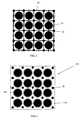
Fig. 2 provides a top view of theinner carbon layer 34 of thetop electrode 10 of an array or matrix of pixel ion chambers. -
Fig. 3 provides a top view of thefirst layer 110 of the segmentedelectrode 100 of an array or matrix of pixel ion chambers. -
Fig. 4 provides a detailed side view of the segmentedelectrode 110. -
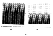
Fig. 5 provides an illustration of the structure of the signal layers 3 and 4 130 and 140. - A monitoring device for measuring radiation in real time is described. The monitoring device can be used for monitoring the fluency rate produced by a radiation device. In operation the monitoring device is positioned between the radiation device and the target, such as a patient receiving radiation treatment. In such a position, the device measures the fluency rate and the corresponding radiation dose can be determined in real time. The following description is of the preferred embodiment of the present invention.
- The monitoring device is made up of an array or matrix of pixel ion chambers.
Fig. 1 shows the side view of the structure of a singlepixel ion chamber 1 constructed in accordance with the present invention. Thepixel ion chamber 1 has atop electrode 10, amid layer 50, and asegmented electrode 100. - The
top electrode 10 has apolyimide layer 20 sandwiched on both sides bycarbon layers - The
outer carbon layer 32 of thetop electrode 10 acts as an Electro-Magnetic Compatibility ("EMC") shield. Theouter carbon layer 32 generally extends across the entire plane of thepixel ion chamber 1. Theinner carbon layer 34 is structured according tohole 55 ofmid layer 50 and dimensioned so that the circumference of the inner carbon layer fits into and is smaller than the circumference of thehole 55. Preferably, theinner carbon layer 34, andhole 55 are substantially circular in shape, (although they could be any shape depending on the application and easy manufacturing) and differ in diameter (with theinner carbon layer 34 being the smaller diameter). In the preferred embodiment the inner carbon layer is about 4.4 mm diameter, and the correspondinghole 55 inmid layer 50 has a diameter of about 4.5 mm. This arrangement assures that themid layer 50 does not come in contact with thecenter electrodes carbon layer 34 are connected to each other by means of a copper grid 36 (as illustrated inFig. 2 ) to assure a good and uniform conductivity. - The
mid layer 50 is constructed of pure polycarbonate plate. Preferably themid layer 50 is about 5 mm thick, but can larger or smaller depending on the diameter of the chamber. In the approximate center ofmid layer 50, ahole 55 extends through the entire thickness of themid layer 50. Thehole 58 is preferably about 4.5 mm in diameter and extends substantially perpendicular to the horizontal plane ofmid layer 50 to form a cylinder. - The
top end 52 ofmid layer 50 is laminated to thepolyimide layer 20 oftop electrode 10 by means of an adhesive 45. Preferably the adhesive is in the form ofadhesive dots 45 that are about 100 µm thick. The adhesive material is preferably epoxy with a diameter from about 1 to 2mm. Thebottom end 56 ofmid layer 50 is likewise laminated to thetop layer 105 of thesegmented electrode 100 by an adhesive 45, which is preferably in the form ofadhesive dots 45. Once themid layer 50 is adhered to the top 20 andsegmented electrode 100,chamber 58 is formed in thehole 55 ofmid layer 50. - The adhesive or
glue dots 45 perform several functions in addition to adhering themid layer 50 to thetop electrode 10 and to thesegmented electrode 100. First the shape and position of thedots 45 is such that it does not entirely seal thechamber 58, but instead provides ventilation slits or open channels on both sides of themid layer 50 for thechamber 58. Theglue dots 45 are positioned around theinner carbon layer 34 of the top electrode, and around thepixels 105 of thesegmented electrode 100. In absolute Dosimetry vented chambers are preferable to sealed chamber, because sealed chambers tend to not to be, or remain, gas tight, which leads to an unpredictable change in sensitivity. - Additionally, the use of a grid of
glue dots 45, as illustrated inFigs. 2 and 3 (which provides the top view of the cell-supporting structure of an array or matrix of pixel ion chambers 1), permits the construction without the use of an external mechanical frame. The elimination of such a frame from the pixel ion chamber array minimizes or eliminates mechanical deformation or microphonic effect that is present when an external frame is used. In this way, the accuracy of the measurements obtained increases over devices that utilize external frames. - The
glue dots 45 also assist in minimizing or eliminatingmid layer 50 leakage that can occur between thetop electrode 10 through themid layer 50 to thesegmented electrode 100. Such leakage disturbs the measurements and its reduction or elimination also increases the accuracy of the measurement. The glue dots act as spacers that prevent themid layer 50 from touching the collecting electrodes, which is one technique of the present invention to reduce leakage. As discussed below, the present invention provides other techniques that may be used alone, or in combination with the use of glue dots, to reduce leakage. - The detailed side view of the segmented electrode is illustrated in
Fig. 4 (not drawn to scale). In the preferred embodiment, thesegmented electrode 100 comprises a six layer printed circuit board. Thefirst layer 110, facing the inside of thechamber 58, is comprised of apixel 105 constructed preferably of carbon print, or alternatively graphite or thin metal. Thepixels 105 are preferably about 25 µm thick. Thepixel 105 is shaped and dimensioned according to the shape and dimension of thehole 55 so that thepixel 105 fits into thehole 55. Preferably, thepixel 105 is substantially circular (although they could be any shape depending on the application and easy manufacturing) with a diameter less than the diameter of thehole 55. In the preferred embodiment, thepixel 105 is about 0.4 mm smaller in diameter than the diameter of thehole 55 inmid layer 50. More preferably, thehole 55 has a diameter of about 4.5 mm and thepixel 105 has a diameter of about 4.1 mm. - The
pixel 105 is connected to the signal tracks, shown inFig. 5 , by a plugged via 108. The plugged via 108 is a vertical interconnection between twoinsulation layers copper cylinder 109 of a thickness of about 20µm created in a galvanic process. The via 108 provides the vertical interconnection through the insulation layers and connects thepixels 105 to the signal tracks. - Directly beneath the
first layer 110 is a layer ofCore material 115 sandwiched by two copper guard tracks 104 and 120. Preferably, thelayer 115 is constructed of pure polyimide, or alternatively glass fiber reinforced Duraver® 156 material, or any low Z PCB material and is about 1000µm thick. This thickness permits Core material to absorb back scattered electrons. These copper tracks are preferably about 18µm thick (unless otherwise noted all copper tracks or layers are preferably about 18 µm thick). The topcopper guard track 104, which in combination with thepixel 105 provides thefirst layer 110 of thesegmented electrode 100. The topcopper guard track 104 is shaped to surround thepixel 105, thereby preventing leakage from thetop electrode 10. The topcopper guard track 104 has holes that correspond to the shape of thepixels 105, but have a larger diameter so it does not overlap thepixels 105. The preferred configuration of the top view of thefirst layer 110 is illustrated inFig. 3 . In the preferred embodiment, the diameter of the holes in the topcopper guard track 104 is about 4.9 mm. This results in an average copper density of around 60 % for the topcopper guard track 104.Adhesive dots 45 are also used to connect thefirst layer 110 of thesegmented electrode 100 to themid layer 50. - The second layer is comprised of the bottom
copper guard track 120 and is positioned on the opposite side of theCore material 115 from that of the topcopper guard track 104. The bottomcopper guard track 120 prevents cross-talk between the signal tracks (not shown) and thepixels 105. Theguard 120 is connected to a potential of low impedance (not shown) that is very close to the sensor input potential (± 1mV). The average copper density of the bottomcopper guard track 120 is about 100%, except that the track does not extend through the plugged via 108. - Sandwiched between the
second layer 120 and thethird layer 130 is aninsulation layer 128, preferably constructed from about a 50µm thick of Polyimide (Pyralux® AP 8525R).Adhesive layers insulation layer 128 of about 25µm thick are provided. - The third and fourth layers and are
copper layers fourth layers pixels 105 to the read out electronics (not shown) on one side of thepixel chamber 1. To reduce leakage, the pixel track, which is comprised of the electrodes and the copper track to the readout electronics, is also surrounded by copper guard tracks (not shown). Preferably the pixel track is surrounded on both sides, as well as on the top by thethird layer 130 and the bottom by thefourth layer 140. The average copper density will preferably be around 50% for the third andfourth layer Fig. 5 illustrates the structure of the signal for layers 3 and 4,130 and 140. - Sandwiched between the
fourth layer 140 and thefifth layer 150 is anotherinsulation layer 148, preferably constructed from about a 50µm thick of Polyimide, such as for example Pyralux® AP 8525R.Adhesive layers insulation layer 148 of about 25µm thick are provided. - The fifth and
sixth layers sixth layers thick polyimide foil 155, such as for example Pyralux® AP 8525R. Layer 5 150 is connected to the guard potential (not shown) and layer 6 160 is connected to a protective ground (not shown) in order to improve the electro-magnetic immunity.. The average copper density is preferably about 100% for bothlayers - In a further embodiment an array of pixel ion chambers is constructed as illustrated in
Figs. 2 and 3 . Use of the glue dots between layers according the invention provides a cell-supporting structure, without a frame. Use of printed carbon electrodes instead of copper, providing a lower Z material, a more transparent chamber is obtained. Further transparency is obtained use of bromide free PCB material (low Z material). Additionally, the use of a printed carbon layer on top of the top electrode acts as an electro-magnetic shield. Finally, the copper tracks as guard layers provide protection from and minimize leakage. - In a further embodiment, the chamber array as provided by the current invention is incorporated into an online monitor for measuring, in real-time, the radiation fluency rate produced by a radiotherapy device. Among the uses for an online monitor of the present invention, is the monitoring of dose delivery of radiation to a patient receiving radiation therapy, and provide dose verification in real-time. In this embodiment, the monitor with chamber array can be positioned between the radiation device and the target; in the case of radiation therapy the target is the patient, because of the improved transparency of the chamber array, a direct measurement of the fluency can be obtained thereby eliminating the need to calculate the dose delivered to the patient by indirect measurements and calculations.
- There will be various modifications, adjustments, and applications of the disclosed invention that will be apparent to those of skill in the art, and the present application is intended to cover such embodiments. Although the present invention has been described in the context of certain preferred embodiments, it is intended that the full scope of these be measured by reference to the scope of the following claims. For example, where the examples show a set of pixels arranged in a matrix, other arrangements of a set of pixels may be contemplated, such as specific arrangements of lines for measuring specific aspects of a beam, such as flatness, skewness, or positions of leaves of a multi-leaf collimator.
Claims (5)
- A radiation monitor comprising: a set of pixel ion chambers (1) wherein the pixel ion chambers (1) comprise a top electrode (10); a segmented electrode (100) connected to the top electrode (10) through a mid layer (50); and a plurality of chambers (58) formed within the mid layer (50) extending from the top electrodes (10) to the segmented electrodes (100); characterised in that the mid layer (50) is laminated to the top electrodes (10) and segmented electrodes (100) by a set of adhesive dots (45), wherein the adhesive dots (45) are dimensioned and positioned on the mid layer (50) to provide ventilation slits or channels for the pixel ion chambers (1).
- The radiation monitor of claim 1 wherein the adhesive dots (45) are formed from epoxy and have a diameter of about 1 to 2 mm.
- The radiation monitor of claim 1 or 2 wherein the top electrodes (10) further comprises an inner printed carbon layer (34) wherein the inner carbon layers (34) are connected by a copper grid (36).
- The radiation monitor of claim 1, 2 or 3 wherein said set of pixel ion chambers (1) are arranged in a matrix.
- A method of monitoring the radiation delivered to a target by a radiation device comprising: positioning the radiation monitor of any of claims 1 to 4 between the radiation device and the target so that the radiation beam travels through the monitor prior to delivering the radiation to the target; delivering the radiation to the target; and measuring the fluency rate produced by a radiation device, wherein the target is a water phantom.
Applications Claiming Priority (2)
| Application Number | Priority Date | Filing Date | Title |
|---|---|---|---|
| US68571205P | 2005-05-27 | 2005-05-27 | |
| PCT/IB2006/001390 WO2006126084A2 (en) | 2005-05-27 | 2006-05-26 | Device and method for quality assurance and online verification of radiation therapy |
Publications (2)
| Publication Number | Publication Date |
|---|---|
| EP1889281A2 EP1889281A2 (en) | 2008-02-20 |
| EP1889281B1 true EP1889281B1 (en) | 2016-11-23 |
Family
ID=36693978
Family Applications (1)
| Application Number | Title | Priority Date | Filing Date |
|---|---|---|---|
| EP06755916.1A Active EP1889281B1 (en) | 2005-05-27 | 2006-05-26 | Device and method for quality assurance and online verification of radiation therapy |
Country Status (5)
| Country | Link |
|---|---|
| US (1) | US7476867B2 (en) |
| EP (1) | EP1889281B1 (en) |
| JP (1) | JP5070501B2 (en) |
| CN (1) | CN101390190B (en) |
| WO (2) | WO2006126075A2 (en) |
Families Citing this family (50)
| Publication number | Priority date | Publication date | Assignee | Title |
|---|---|---|---|---|
| CN101061759B (en) * | 2004-07-21 | 2011-05-25 | 斯蒂尔瑞弗系统有限公司 | Programmable RF Waveform Generator for Synchrocyclotrons |
| EP2389977A3 (en) | 2005-11-18 | 2012-01-25 | Still River Systems, Inc. | Charged particle radiation therapy |
| EP1917998A1 (en) * | 2006-11-03 | 2008-05-07 | Ion Beam Applications S.A. | Method and device for online IMRT verification |
| US7413345B1 (en) * | 2007-04-11 | 2008-08-19 | Keith Spanswick | Calibration device and method of using same |
| US8130905B1 (en) | 2007-11-21 | 2012-03-06 | Sun Nuclear Corporation | Dosimetry system and method for radiation therapy |
| US8581523B2 (en) | 2007-11-30 | 2013-11-12 | Mevion Medical Systems, Inc. | Interrupted particle source |
| US8933650B2 (en) * | 2007-11-30 | 2015-01-13 | Mevion Medical Systems, Inc. | Matching a resonant frequency of a resonant cavity to a frequency of an input voltage |
| JP5687265B2 (en) * | 2009-03-20 | 2015-03-18 | イオン・ビーム・アプリケーションズ・エス・アー | Device for dosimetric monitoring of hadron beam and method for monitoring hadron beam |
| BE1018836A3 (en) * | 2009-07-24 | 2011-09-06 | Ion Beam Applic Sa | DEVICE AND METHOD FOR MEASURING AN ENERGY BEAM. |
| JP2013506823A (en) | 2009-10-01 | 2013-02-28 | イオン・ビーム・アプリケーションズ・エス・アー | Energy beam line control apparatus and method |
| EP3460529B1 (en) | 2012-05-29 | 2025-05-14 | Sun Nuclear Corporation | System for calorimetry probe |
| JP6121544B2 (en) | 2012-09-28 | 2017-04-26 | メビオン・メディカル・システムズ・インコーポレーテッド | Particle beam focusing |
| JP6254600B2 (en) | 2012-09-28 | 2017-12-27 | メビオン・メディカル・システムズ・インコーポレーテッド | Particle accelerator |
| TW201422278A (en) | 2012-09-28 | 2014-06-16 | Mevion Medical Systems Inc | Control system for a particle accelerator |
| US10254739B2 (en) | 2012-09-28 | 2019-04-09 | Mevion Medical Systems, Inc. | Coil positioning system |
| ES2739634T3 (en) | 2012-09-28 | 2020-02-03 | Mevion Medical Systems Inc | Particle therapy control |
| CN104813749B (en) | 2012-09-28 | 2019-07-02 | 梅维昂医疗系统股份有限公司 | Control the intensity of the particle beam |
| CN108770178B (en) | 2012-09-28 | 2021-04-16 | 迈胜医疗设备有限公司 | Magnetic Field Regenerator |
| JP6523957B2 (en) | 2012-09-28 | 2019-06-05 | メビオン・メディカル・システムズ・インコーポレーテッド | Magnetic shim for changing the magnetic field |
| EP2900325B1 (en) | 2012-09-28 | 2018-01-03 | Mevion Medical Systems, Inc. | Adjusting energy of a particle beam |
| US9721772B2 (en) * | 2013-01-25 | 2017-08-01 | General Electric Company | Ion chamber enclosure material to increase gamma radiation sensitivity |
| US8791656B1 (en) | 2013-05-31 | 2014-07-29 | Mevion Medical Systems, Inc. | Active return system |
| US9730308B2 (en) | 2013-06-12 | 2017-08-08 | Mevion Medical Systems, Inc. | Particle accelerator that produces charged particles having variable energies |
| DE102013011077A1 (en) * | 2013-07-03 | 2015-01-08 | Peter Koller | Detector plate for radiation analysis and production process thereof |
| ES2768659T3 (en) | 2013-09-27 | 2020-06-23 | Mevion Medical Systems Inc | Particle beam scanning |
| EP2878976A1 (en) * | 2013-11-30 | 2015-06-03 | Ion Beam Applications S.A. | Device and method for radiation dosimetry based on a ionization chamber |
| US10675487B2 (en) | 2013-12-20 | 2020-06-09 | Mevion Medical Systems, Inc. | Energy degrader enabling high-speed energy switching |
| US9962560B2 (en) | 2013-12-20 | 2018-05-08 | Mevion Medical Systems, Inc. | Collimator and energy degrader |
| US9661736B2 (en) | 2014-02-20 | 2017-05-23 | Mevion Medical Systems, Inc. | Scanning system for a particle therapy system |
| US9950194B2 (en) | 2014-09-09 | 2018-04-24 | Mevion Medical Systems, Inc. | Patient positioning system |
| US10099067B2 (en) | 2014-12-19 | 2018-10-16 | Sun Nuclear Corporation | Radiation therapy dose calculation |
| US10617891B2 (en) | 2015-04-23 | 2020-04-14 | Sun Nuclear Corporation | Radiation detector calibration |
| US10786689B2 (en) | 2015-11-10 | 2020-09-29 | Mevion Medical Systems, Inc. | Adaptive aperture |
| WO2018009779A1 (en) | 2016-07-08 | 2018-01-11 | Mevion Medical Systems, Inc. | Treatment planning |
| US10596394B2 (en) | 2016-07-28 | 2020-03-24 | Sun Nuclear Corporation | Beam angle direction determination |
| TR201611175A3 (en) | 2016-08-09 | 2018-03-21 | Deniz Celik | LİNAK QUALITY CONTROLLER |
| US11103730B2 (en) | 2017-02-23 | 2021-08-31 | Mevion Medical Systems, Inc. | Automated treatment in particle therapy |
| WO2018160763A1 (en) | 2017-02-28 | 2018-09-07 | Sun Nuclear Corporation | Radiation therapy treatment verification with electronic portal imaging device transit images |
| WO2019006253A1 (en) | 2017-06-30 | 2019-01-03 | Mevion Medical Systems, Inc. | Configurable collimator controlled using linear motors |
| CN107456664B (en) * | 2017-08-22 | 2021-05-11 | 哈尔滨工程大学 | A hemispherical retractable 3D fiber accelerator morning detector |
| US11278744B2 (en) | 2018-09-28 | 2022-03-22 | Sun Nuclear Corporation | Systems and methods to account for tilt of a radiation measurement system |
| CN113196414B (en) | 2018-10-12 | 2025-04-25 | 医科达有限公司 | Quality Assurance for MR-LINAC |
| EP3934752A1 (en) | 2019-03-08 | 2022-01-12 | Mevion Medical Systems, Inc. | Delivery of radiation by column and generating a treatment plan therefor |
| US12011616B2 (en) | 2019-07-10 | 2024-06-18 | Sun Nuclear Corporation | Image-based radiation therapy quality assurance |
| US11600004B2 (en) | 2019-07-10 | 2023-03-07 | Sun Nuclear Corporation | Image-based radiation therapy quality assurance |
| WO2021007459A1 (en) | 2019-07-10 | 2021-01-14 | Sun Nuclear Corporation | Scintillator-based radiation therapy quality assurance |
| US12201850B2 (en) | 2022-06-16 | 2025-01-21 | Sun Nuclear Corporation | High dose rate radiation therapy systems and dosimetry |
| US12544596B2 (en) | 2023-03-30 | 2026-02-10 | Sun Nuclear Corporation | Adjustable radiation detector support |
| EP4579284A1 (en) | 2023-12-26 | 2025-07-02 | Ion Beam Applications | Hybrid 2d-detector |
| CN119364631B (en) * | 2024-12-23 | 2025-03-18 | 中玖闪光医疗科技有限公司 | Low-pressure ionization chamber, design method and medical linear accelerator |
Family Cites Families (11)
| Publication number | Priority date | Publication date | Assignee | Title |
|---|---|---|---|---|
| US4075527A (en) * | 1976-09-27 | 1978-02-21 | General Electric Company | X-ray detector |
| US4686369A (en) * | 1985-12-13 | 1987-08-11 | General Electric Company | Electric shielding for kinestatic charge detector |
| US5162450A (en) * | 1989-02-17 | 1992-11-10 | General Electric Company | Curable dielectric polyphenylene ether-polyepoxide compositions |
| JP2723391B2 (en) * | 1991-08-02 | 1998-03-09 | 三菱電機株式会社 | Charged particle beam monitor |
| FR2727525B1 (en) * | 1994-11-25 | 1997-01-10 | Centre Nat Rech Scient | IONIZING RADIATION DETECTOR WITH PROPORTIONAL MICROCOUNTERS |
| US5631470A (en) * | 1996-05-13 | 1997-05-20 | Varian Associates, Inc. | Liquid ion chamber electrode apparatus |
| WO1999021211A1 (en) * | 1997-10-22 | 1999-04-29 | European Organization For Nuclear Research | Radiation detector of very high performance and planispherical parallax-free x-ray imager comprising such a radiation detector |
| DE19811556A1 (en) * | 1998-03-17 | 1999-09-23 | Philips Patentverwaltung | Radiation measuring device with an ionization chamber |
| US6429578B1 (en) * | 1999-01-26 | 2002-08-06 | Mats Danielsson | Diagnostic and therapeutic detector system for imaging with low and high energy X-ray and electrons |
| US6545422B1 (en) * | 2000-10-27 | 2003-04-08 | Science Applications International Corporation | Socket for use with a micro-component in a light-emitting panel |
| US7189975B2 (en) * | 2004-02-09 | 2007-03-13 | Standard Imaging, Inc. | Wire-free, dual-mode calibration instrument for high energy therapeutic radiation |
-
2006
- 2006-05-25 WO PCT/IB2006/001365 patent/WO2006126075A2/en not_active Ceased
- 2006-05-25 US US11/440,890 patent/US7476867B2/en active Active
- 2006-05-26 EP EP06755916.1A patent/EP1889281B1/en active Active
- 2006-05-26 CN CN2006800177734A patent/CN101390190B/en active Active
- 2006-05-26 JP JP2008512947A patent/JP5070501B2/en active Active
- 2006-05-26 WO PCT/IB2006/001390 patent/WO2006126084A2/en not_active Ceased
Also Published As
| Publication number | Publication date |
|---|---|
| US7476867B2 (en) | 2009-01-13 |
| US20060266951A1 (en) | 2006-11-30 |
| JP2009507521A (en) | 2009-02-26 |
| WO2006126075A2 (en) | 2006-11-30 |
| WO2006126075A3 (en) | 2007-08-23 |
| JP5070501B2 (en) | 2012-11-14 |
| CN101390190B (en) | 2011-10-05 |
| WO2006126084A3 (en) | 2007-08-23 |
| EP1889281A2 (en) | 2008-02-20 |
| CN101390190A (en) | 2009-03-18 |
| WO2006126084A2 (en) | 2006-11-30 |
Similar Documents
| Publication | Publication Date | Title |
|---|---|---|
| US7476867B2 (en) | Device and method for quality assurance and online verification of radiation therapy | |
| JP5270659B2 (en) | Apparatus, use and method for online dose monitoring of hadron beams | |
| EP3862795B1 (en) | Method for monitoring a proton beam | |
| CN101257945B (en) | Dosimetry devices for testing radiotherapy equipment | |
| US7030386B2 (en) | High quantum efficiency x-ray detector for portal imaging | |
| JP5247589B2 (en) | Ionization chamber detector and dose distribution measuring device | |
| US20120310030A1 (en) | Device And Method For Line Control Of An Energy Beam | |
| US20170003403A1 (en) | Device and method for radiation dosimetry | |
| US11385360B2 (en) | Sensors with virtual spatial sensitivity for monitoring a radiation generating device | |
| JP5791795B2 (en) | Radiation measurement equipment | |
| JPH0658403B2 (en) | Radioactivity distribution measuring device | |
| Eichin et al. | Development and evaluation of a pixel detector system for pencil beam scanning proton therapy | |
| EP4579284A1 (en) | Hybrid 2d-detector | |
| CN204556839U (en) | Based on the semiconductor detector array of FPC |
Legal Events
| Date | Code | Title | Description |
|---|---|---|---|
| PUAI | Public reference made under article 153(3) epc to a published international application that has entered the european phase |
Free format text: ORIGINAL CODE: 0009012 |
|
| AK | Designated contracting states |
Kind code of ref document: A2 Designated state(s): AT BE BG CH CY CZ DE DK EE ES FI FR GB GR HU IE IS IT LI LT LU LV MC NL PL PT RO SE SI SK TR |
|
| AX | Request for extension of the european patent |
Extension state: AL BA HR MK YU |
|
| 17P | Request for examination filed |
Effective date: 20080225 |
|
| RBV | Designated contracting states (corrected) |
Designated state(s): AT BE BG CH CY CZ DE DK EE ES FI FR GB GR HU IE IS IT LI LT LU LV MC NL PL PT RO SE SI SK TR |
|
| RIN1 | Information on inventor provided before grant (corrected) |
Inventor name: FRITSCH, ERNST Inventor name: PERONI, CRISTIANA Inventor name: FRIEDL, FRIEDRICH Inventor name: DONETTI, MARCO Inventor name: MARCHETTO, FLAVIO Inventor name: GOMOLA, IGOR Inventor name: CIRIO, ROBERTO |
|
| DAX | Request for extension of the european patent (deleted) | ||
| 17Q | First examination report despatched |
Effective date: 20141219 |
|
| GRAP | Despatch of communication of intention to grant a patent |
Free format text: ORIGINAL CODE: EPIDOSNIGR1 |
|
| RIC1 | Information provided on ipc code assigned before grant |
Ipc: H01J 47/02 20060101AFI20160530BHEP Ipc: A61N 5/10 20060101ALI20160530BHEP Ipc: G01T 1/29 20060101ALI20160530BHEP |
|
| INTG | Intention to grant announced |
Effective date: 20160617 |
|
| GRAS | Grant fee paid |
Free format text: ORIGINAL CODE: EPIDOSNIGR3 |
|
| GRAA | (expected) grant |
Free format text: ORIGINAL CODE: 0009210 |
|
| AK | Designated contracting states |
Kind code of ref document: B1 Designated state(s): AT BE BG CH CY CZ DE DK EE ES FI FR GB GR HU IE IS IT LI LT LU LV MC NL PL PT RO SE SI SK TR |
|
| REG | Reference to a national code |
Ref country code: GB Ref legal event code: FG4D |
|
| REG | Reference to a national code |
Ref country code: CH Ref legal event code: EP |
|
| REG | Reference to a national code |
Ref country code: IE Ref legal event code: FG4D |
|
| REG | Reference to a national code |
Ref country code: AT Ref legal event code: REF Ref document number: 848578 Country of ref document: AT Kind code of ref document: T Effective date: 20161215 |
|
| REG | Reference to a national code |
Ref country code: NL Ref legal event code: FP |
|
| REG | Reference to a national code |
Ref country code: DE Ref legal event code: R096 Ref document number: 602006051014 Country of ref document: DE |
|
| PG25 | Lapsed in a contracting state [announced via postgrant information from national office to epo] |
Ref country code: LV Free format text: LAPSE BECAUSE OF FAILURE TO SUBMIT A TRANSLATION OF THE DESCRIPTION OR TO PAY THE FEE WITHIN THE PRESCRIBED TIME-LIMIT Effective date: 20161123 |
|
| REG | Reference to a national code |
Ref country code: LT Ref legal event code: MG4D |
|
| REG | Reference to a national code |
Ref country code: AT Ref legal event code: MK05 Ref document number: 848578 Country of ref document: AT Kind code of ref document: T Effective date: 20161123 |
|
| PG25 | Lapsed in a contracting state [announced via postgrant information from national office to epo] |
Ref country code: GR Free format text: LAPSE BECAUSE OF FAILURE TO SUBMIT A TRANSLATION OF THE DESCRIPTION OR TO PAY THE FEE WITHIN THE PRESCRIBED TIME-LIMIT Effective date: 20170224 Ref country code: LT Free format text: LAPSE BECAUSE OF FAILURE TO SUBMIT A TRANSLATION OF THE DESCRIPTION OR TO PAY THE FEE WITHIN THE PRESCRIBED TIME-LIMIT Effective date: 20161123 Ref country code: SE Free format text: LAPSE BECAUSE OF FAILURE TO SUBMIT A TRANSLATION OF THE DESCRIPTION OR TO PAY THE FEE WITHIN THE PRESCRIBED TIME-LIMIT Effective date: 20161123 |
|
| REG | Reference to a national code |
Ref country code: FR Ref legal event code: PLFP Year of fee payment: 12 |
|
| PG25 | Lapsed in a contracting state [announced via postgrant information from national office to epo] |
Ref country code: PL Free format text: LAPSE BECAUSE OF FAILURE TO SUBMIT A TRANSLATION OF THE DESCRIPTION OR TO PAY THE FEE WITHIN THE PRESCRIBED TIME-LIMIT Effective date: 20161123 Ref country code: FI Free format text: LAPSE BECAUSE OF FAILURE TO SUBMIT A TRANSLATION OF THE DESCRIPTION OR TO PAY THE FEE WITHIN THE PRESCRIBED TIME-LIMIT Effective date: 20161123 Ref country code: PT Free format text: LAPSE BECAUSE OF FAILURE TO SUBMIT A TRANSLATION OF THE DESCRIPTION OR TO PAY THE FEE WITHIN THE PRESCRIBED TIME-LIMIT Effective date: 20170323 Ref country code: ES Free format text: LAPSE BECAUSE OF FAILURE TO SUBMIT A TRANSLATION OF THE DESCRIPTION OR TO PAY THE FEE WITHIN THE PRESCRIBED TIME-LIMIT Effective date: 20161123 Ref country code: AT Free format text: LAPSE BECAUSE OF FAILURE TO SUBMIT A TRANSLATION OF THE DESCRIPTION OR TO PAY THE FEE WITHIN THE PRESCRIBED TIME-LIMIT Effective date: 20161123 |
|
| PG25 | Lapsed in a contracting state [announced via postgrant information from national office to epo] |
Ref country code: SK Free format text: LAPSE BECAUSE OF FAILURE TO SUBMIT A TRANSLATION OF THE DESCRIPTION OR TO PAY THE FEE WITHIN THE PRESCRIBED TIME-LIMIT Effective date: 20161123 Ref country code: DK Free format text: LAPSE BECAUSE OF FAILURE TO SUBMIT A TRANSLATION OF THE DESCRIPTION OR TO PAY THE FEE WITHIN THE PRESCRIBED TIME-LIMIT Effective date: 20161123 Ref country code: RO Free format text: LAPSE BECAUSE OF FAILURE TO SUBMIT A TRANSLATION OF THE DESCRIPTION OR TO PAY THE FEE WITHIN THE PRESCRIBED TIME-LIMIT Effective date: 20161123 Ref country code: CZ Free format text: LAPSE BECAUSE OF FAILURE TO SUBMIT A TRANSLATION OF THE DESCRIPTION OR TO PAY THE FEE WITHIN THE PRESCRIBED TIME-LIMIT Effective date: 20161123 Ref country code: EE Free format text: LAPSE BECAUSE OF FAILURE TO SUBMIT A TRANSLATION OF THE DESCRIPTION OR TO PAY THE FEE WITHIN THE PRESCRIBED TIME-LIMIT Effective date: 20161123 |
|
| REG | Reference to a national code |
Ref country code: DE Ref legal event code: R097 Ref document number: 602006051014 Country of ref document: DE |
|
| PG25 | Lapsed in a contracting state [announced via postgrant information from national office to epo] |
Ref country code: LU Free format text: LAPSE BECAUSE OF NON-PAYMENT OF DUE FEES Effective date: 20170531 Ref country code: IT Free format text: LAPSE BECAUSE OF FAILURE TO SUBMIT A TRANSLATION OF THE DESCRIPTION OR TO PAY THE FEE WITHIN THE PRESCRIBED TIME-LIMIT Effective date: 20161123 Ref country code: BG Free format text: LAPSE BECAUSE OF FAILURE TO SUBMIT A TRANSLATION OF THE DESCRIPTION OR TO PAY THE FEE WITHIN THE PRESCRIBED TIME-LIMIT Effective date: 20170223 |
|
| PLBE | No opposition filed within time limit |
Free format text: ORIGINAL CODE: 0009261 |
|
| STAA | Information on the status of an ep patent application or granted ep patent |
Free format text: STATUS: NO OPPOSITION FILED WITHIN TIME LIMIT |
|
| 26N | No opposition filed |
Effective date: 20170824 |
|
| PG25 | Lapsed in a contracting state [announced via postgrant information from national office to epo] |
Ref country code: SI Free format text: LAPSE BECAUSE OF FAILURE TO SUBMIT A TRANSLATION OF THE DESCRIPTION OR TO PAY THE FEE WITHIN THE PRESCRIBED TIME-LIMIT Effective date: 20161123 |
|
| REG | Reference to a national code |
Ref country code: CH Ref legal event code: PL |
|
| PG25 | Lapsed in a contracting state [announced via postgrant information from national office to epo] |
Ref country code: MC Free format text: LAPSE BECAUSE OF FAILURE TO SUBMIT A TRANSLATION OF THE DESCRIPTION OR TO PAY THE FEE WITHIN THE PRESCRIBED TIME-LIMIT Effective date: 20161123 |
|
| REG | Reference to a national code |
Ref country code: IE Ref legal event code: MM4A |
|
| PG25 | Lapsed in a contracting state [announced via postgrant information from national office to epo] |
Ref country code: LI Free format text: LAPSE BECAUSE OF NON-PAYMENT OF DUE FEES Effective date: 20170531 Ref country code: CH Free format text: LAPSE BECAUSE OF NON-PAYMENT OF DUE FEES Effective date: 20170531 |
|
| PG25 | Lapsed in a contracting state [announced via postgrant information from national office to epo] |
Ref country code: LU Free format text: LAPSE BECAUSE OF NON-PAYMENT OF DUE FEES Effective date: 20170526 |
|
| PG25 | Lapsed in a contracting state [announced via postgrant information from national office to epo] |
Ref country code: IE Free format text: LAPSE BECAUSE OF NON-PAYMENT OF DUE FEES Effective date: 20170526 |
|
| REG | Reference to a national code |
Ref country code: FR Ref legal event code: PLFP Year of fee payment: 13 |
|
| PG25 | Lapsed in a contracting state [announced via postgrant information from national office to epo] |
Ref country code: HU Free format text: LAPSE BECAUSE OF FAILURE TO SUBMIT A TRANSLATION OF THE DESCRIPTION OR TO PAY THE FEE WITHIN THE PRESCRIBED TIME-LIMIT; INVALID AB INITIO Effective date: 20060526 |
|
| PG25 | Lapsed in a contracting state [announced via postgrant information from national office to epo] |
Ref country code: CY Free format text: LAPSE BECAUSE OF NON-PAYMENT OF DUE FEES Effective date: 20161123 |
|
| PG25 | Lapsed in a contracting state [announced via postgrant information from national office to epo] |
Ref country code: TR Free format text: LAPSE BECAUSE OF FAILURE TO SUBMIT A TRANSLATION OF THE DESCRIPTION OR TO PAY THE FEE WITHIN THE PRESCRIBED TIME-LIMIT Effective date: 20161123 |
|
| PG25 | Lapsed in a contracting state [announced via postgrant information from national office to epo] |
Ref country code: IS Free format text: LAPSE BECAUSE OF FAILURE TO SUBMIT A TRANSLATION OF THE DESCRIPTION OR TO PAY THE FEE WITHIN THE PRESCRIBED TIME-LIMIT Effective date: 20170323 |
|
| PGFP | Annual fee paid to national office [announced via postgrant information from national office to epo] |
Ref country code: NL Payment date: 20250526 Year of fee payment: 20 |
|
| PGFP | Annual fee paid to national office [announced via postgrant information from national office to epo] |
Ref country code: DE Payment date: 20250529 Year of fee payment: 20 |
|
| PGFP | Annual fee paid to national office [announced via postgrant information from national office to epo] |
Ref country code: GB Payment date: 20250527 Year of fee payment: 20 |
|
| PGFP | Annual fee paid to national office [announced via postgrant information from national office to epo] |
Ref country code: BE Payment date: 20250527 Year of fee payment: 20 |
|
| PGFP | Annual fee paid to national office [announced via postgrant information from national office to epo] |
Ref country code: FR Payment date: 20250526 Year of fee payment: 20 |