EP1887704B1 - A chassis - Google Patents
A chassis Download PDFInfo
- Publication number
- EP1887704B1 EP1887704B1 EP06761498A EP06761498A EP1887704B1 EP 1887704 B1 EP1887704 B1 EP 1887704B1 EP 06761498 A EP06761498 A EP 06761498A EP 06761498 A EP06761498 A EP 06761498A EP 1887704 B1 EP1887704 B1 EP 1887704B1
- Authority
- EP
- European Patent Office
- Prior art keywords
- chassis
- cables
- main body
- fan
- slide rail
- Prior art date
- Legal status (The legal status is an assumption and is not a legal conclusion. Google has not performed a legal analysis and makes no representation as to the accuracy of the status listed.)
- Not-in-force
Links
Images
Classifications
-
- H—ELECTRICITY
- H04—ELECTRIC COMMUNICATION TECHNIQUE
- H04B—TRANSMISSION
- H04B1/00—Details of transmission systems, not covered by a single one of groups H04B3/00 - H04B13/00; Details of transmission systems not characterised by the medium used for transmission
- H04B1/02—Transmitters
- H04B1/03—Constructional details, e.g. casings, housings
-
- G—PHYSICS
- G06—COMPUTING OR CALCULATING; COUNTING
- G06F—ELECTRIC DIGITAL DATA PROCESSING
- G06F1/00—Details not covered by groups G06F3/00 - G06F13/00 and G06F21/00
- G06F1/16—Constructional details or arrangements
- G06F1/18—Packaging or power distribution
- G06F1/183—Internal mounting support structures, e.g. for supporting printed circuit boards
-
- H—ELECTRICITY
- H05—ELECTRIC TECHNIQUES NOT OTHERWISE PROVIDED FOR
- H05K—PRINTED CIRCUITS; CASINGS OR CONSTRUCTIONAL DETAILS OF ELECTRIC APPARATUS; MANUFACTURE OF ASSEMBLAGES OF ELECTRICAL COMPONENTS
- H05K7/00—Constructional details common to different types of electric apparatus
- H05K7/14—Mounting supporting structure in casing or on frame or rack
- H05K7/1438—Back panels or connecting means therefor; Terminals; Coding means to avoid wrong insertion
- H05K7/1447—External wirings; Wiring ducts; Laying cables
- H05K7/1449—External wirings; Wiring ducts; Laying cables with connections to the back board
Definitions
- the present invention relates to the manufacturing of communication, electronic and electrical equipments, and particularly to a chassis for accommodating communication and electronic devices or modules.
- chassis In communication systems as well as electronic and electrical equipments, chassis is commonly used to accommodate single boards, fans and all kinds of elements.
- the chassis which has a compact configuration and can be easily assembled and unassembled is becoming increasingly popular.
- FIG. 1 a typical integrated chassis allowing plug-in unit plugging from both front and rear sides is illustrated in Figure 1 .
- Single boards 3 and 4 are plugged into the chassis so that they occupy the full width of the chassis. Therefore, to achieve a compact chassis with reliable heat dissipation, there is a need to provide a fan and a power distribution unit in the chassis, for example, a fan 1 is arranged at the upper position of the chassis and a power distribution unit 5 is arranged at the lower position of the chassis.
- the power supply solution for the fan is designed to provide a backplane 2 extending to the fan region, provide a fan connector plugged into the backplane 2 directly, arrange a power supply path in the backplane 2 and thus lead electrical power from the lower position to the upper position via the backplane to supply the fan.
- the above solution may satisfy the requirements in a certain extent.
- the backplane is equipped with connectors for single boards and the available space is limited. It is difficult to preset the space for the power supply path in the design process, especially when a large current is required. Accordingly, there is a problem that the prior chassis configuration is not reasonable.
- One object of the present invention is to provide a chassis with an improved configuration.
- the present invention provides a chassis, which includes a main body including a backplane, a top cover plate, a bottom cover plate and two side plates.
- a device configured to arrange cables is defined in at least one of the two side plates of the chassis, and the cables are configured to connect a first component of the chassis with a second component having a distance from the first component.
- the device configured to arrange the cables includes a groove defined in the inner of the at least one of the two side plates, and the space surrounded by the groove is configured to contain the cables.
- the device configured to arrange the cables further includes a cable routing cover configured to cover the cables within the groove.
- the cable routing cover is a rectangular flat plate.
- the device configured to arrange the cables includes a first opening defined in at least one of the two side plates at an upper position and a second opening defined in the at least one of the two side plates at a lower position, and the cables pass through the first opening and the second opening to connect the first component with the second component.
- the first component is a fan unit arranged at an upper position of the main body and the second component is a power distribution unit arranged at a lower position of the main body, one end of the cables is connected to the fan unit and the other end of the cables is connected to the power distribution unit.
- the device configured to arrange the cables further includes a cable routing cover adapted to cover the cables exposed outside of the chassis.
- the cable routing cover is an elongated, peripherally closed sheath.
- the cable routing cover is provided with elastic conductors along the inner peripheral thereof.
- an upper functional unit and a lower functional unit of the integrated chassis may be easily connected via cables, without providing any circuit path in the backplane. Therefore, the structure of the backplane may be simplified, and the manufacturing cost may be reduced. Meanwhile, the cable routing cover may cover the cables to provide a good protection and shielding therefor.
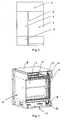
- FIG 1 is a side view of an integrated chassis allowing plugging plug-in unit from both front and rear sides.
- the chassis of the present invention includes a fan 1 and a power distribution unit 5 (installation regions thereof rather than physical objects are shown in the Figure), and the fan 1 is arranged at the upper position of the chassis and the power distribution unit 5 is arranged at the lower position of the chassis.
- the chassis further comprises a front plugboard 3 arranged on the left side within the chassis, a back plugboard 4 arranged on the right side within the chassis, and a backplane 2 perpendicularly arranged between the front plugboard 3 and the back plugboard 4.
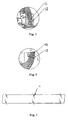
- FIG. 2 is a perspective view of the chassis according to the present invention.
- the chassis according to the present invention includes a main body formed by a backplane 2, a top cover plate 6, a bottom cover plate 15, a left side plate 16 and a right side plate 9 connected with each other.
- the chassis further includes slide rail for securing single boards (the array of the single boards not shown), e.g., an upper slide rail 7 and a lower slide rail 10 parallel to the top and bottom cover plates are arranged in the upper region and the lower region of the main body, respectively.
- a side plate groove 12 extending from the upper position to the lower position is formed on the inner side of the side plate 9.
- the groove may be semi-circle, square, U-shaped, or any other shape suitable to accommodate cables.
- the main body further includes a cable routing cover 8 used to cover the cables 11 within the side plate groove 12 and achieve a good protection and shielding.
- FIG 3 is a partially enlarged view of a portion "A" indicated in Figure 2 .
- the cables 11 pass through the upper slide rail 7 to run in the side plate groove 12.
- FIG 4 is a partially enlarged view of a portion "B" indicated in Figure 2 .
- the cables 11 pass by the lower slide rail 10 to come out from the side plate groove 12.
- the region where single boards is arranged is bypassed and there is thus no need to pass across single boards, thereby simplifying the structure of the main body and reducing the difficulty of adding or removing the single boards.
- FIG. 5 is a structural diagram of a cable routing cover according to the present invention.
- the cable routing cover 8 is a rectangular, flat plate with screw holes 51 therein.
- the groups are symmetrically arranged along the two sides of the cable routing cover.
- the screw holes are shown as circular in figure 5 , other shape such as hexagon is also possible. Screws pass through the six screw holes to secure the cable routing cover to the inner side of the side plate.
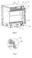
- FIG. 6 is a perspective view of a chassis according to another embodiment of the present invention. As shown in Figure 6 , the present embodiment is different from embodiment 1 in that the configuration for connecting the fan and the power distribution unit is different. Two openings are defined in the side plate 9 at an upper position and a lower position, respectively. Cables 11 pass through the two openings to connect the fan 1 with the power distribution unit 5.
- the chassis is also provided with a cable routing cover 61 for covering the cables 11 from the outside to achieve a good protection and shielding.
- Figure 7 illustrates a partially enlarged view of a portion "C" indicated in Figure 6 .
- the cables 11 pass through the opening 13 of the upper side plate to come out from the main body.
- FIG 8 is a partially enlarged view of a portion "D" indicated in Figure 6 .
- the cables 11 pass through the opening 14 of the lower side plate to come into the main body.
- the openings 13 and 14 are shown as square. Other shapes suitable for passage of cables, such as circle or ellipse, are also possible.
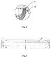
- Figure 9 is a structural diagram of a cable routing cover used in the chassis according to another embodiment of the present invention.
- the cable routing cover is an elongated, peripherally closed sheath.
- Elastic conductors such as conductive fabrics or spring leafs are adhered to the inner peripheral wall 91 of the elongated sheath. The elastic conductors allow a close contact between the cable routing cover and the side plate of the chassis so as to achieve a better shielding.
- the fan 1 and the power distribution unit 5 are interconnected via the cables arranged within the groove so that power may be supplied to the fan. According to the present invention, the requirement to supply power to an upper-arranged fan from a lower-arranged power supply can be satisfied. Therefore, the structure of backplane may be simplified, and the manufacturing cost may be greatly reduced.
Landscapes
- Engineering & Computer Science (AREA)
- Theoretical Computer Science (AREA)
- General Engineering & Computer Science (AREA)
- General Physics & Mathematics (AREA)
- Computer Hardware Design (AREA)
- Power Engineering (AREA)
- Human Computer Interaction (AREA)
- Physics & Mathematics (AREA)
- Computer Networks & Wireless Communication (AREA)
- Signal Processing (AREA)
- Microelectronics & Electronic Packaging (AREA)
- Insertion, Bundling And Securing Of Wires For Electric Apparatuses (AREA)
- Glass Compositions (AREA)
- Patch Boards (AREA)
- Distribution Board (AREA)
- Mounting Of Printed Circuit Boards And The Like (AREA)
Abstract
Description
- The present invention relates to the manufacturing of communication, electronic and electrical equipments, and particularly to a chassis for accommodating communication and electronic devices or modules.
- In communication systems as well as electronic and electrical equipments, chassis is commonly used to accommodate single boards, fans and all kinds of elements. The chassis which has a compact configuration and can be easily assembled and unassembled is becoming increasingly popular.
- In order to satisfy the various user requirements, integrated chassis allowing plugging plug-in unit from both front and rear sides are more and more widely used. In the prior art, a typical integrated chassis allowing plug-in unit plugging from both front and rear sides is illustrated in
Figure 1 .Single boards fan 1 is arranged at the upper position of the chassis and apower distribution unit 5 is arranged at the lower position of the chassis. In such a chassis, the power supply solution for the fan is designed to provide abackplane 2 extending to the fan region, provide a fan connector plugged into thebackplane 2 directly, arrange a power supply path in thebackplane 2 and thus lead electrical power from the lower position to the upper position via the backplane to supply the fan. - The above solution may satisfy the requirements in a certain extent. However, the backplane is equipped with connectors for single boards and the available space is limited. It is difficult to preset the space for the power supply path in the design process, especially when a large current is required. Accordingly, there is a problem that the prior chassis configuration is not reasonable.
- One object of the present invention is to provide a chassis with an improved configuration.
- The object is achieved with the subject-matter of the independent patent claim. Further developments are the subject-matter of the dependent patent claims.
- The present invention provides a chassis, which includes a main body including a backplane, a top cover plate, a bottom cover plate and two side plates. A device configured to arrange cables is defined in at least one of the two side plates of the chassis, and the cables are configured to connect a first component of the chassis with a second component having a distance from the first component.
- More preferably, the device configured to arrange the cables includes a groove defined in the inner of the at least one of the two side plates, and the space surrounded by the groove is configured to contain the cables.
- More preferably, the device configured to arrange the cables further includes a cable routing cover configured to cover the cables within the groove.
- More preferably, the cable routing cover is a rectangular flat plate.
- More preferably, the device configured to arrange the cables includes a first opening defined in at least one of the two side plates at an upper position and a second opening defined in the at least one of the two side plates at a lower position, and the cables pass through the first opening and the second opening to connect the first component with the second component.
- More preferably, the first component is a fan unit arranged at an upper position of the main body and the second component is a power distribution unit arranged at a lower position of the main body, one end of the cables is connected to the fan unit and the other end of the cables is connected to the power distribution unit.
- More preferably, the device configured to arrange the cables further includes a cable routing cover adapted to cover the cables exposed outside of the chassis.
- More preferably, the cable routing cover is an elongated, peripherally closed sheath.
- More preferably, the cable routing cover is provided with elastic conductors along the inner peripheral thereof.
- With either of the two types of structures, an upper functional unit and a lower functional unit of the integrated chassis may be easily connected via cables, without providing any circuit path in the backplane. Therefore, the structure of the backplane may be simplified, and the manufacturing cost may be reduced. Meanwhile, the cable routing cover may cover the cables to provide a good protection and shielding therefor.
- The present invention will be described in more detail hereinafter in conjunction with embodiments with reference to accompanying figures.
-
Figure 1 illustrates a side view of an integrated chassis allowing plug-in unit plugging plug-in unit from both front and rear sides; -
Figure 2 illustrates a perspective view of a chassis according to one embodiment of the present invention; -
Figure 3 illustrates a partially enlarged view of a portion "A" indicated inFigure 2 ; -
Figure 4 illustrates a partially enlarged view of a portion "B" indicated inFigure 2 ; -
Figure 5 illustrates a structural diagram of a cable routing cover according to the embodiment of the present invention; -
Figure 6 illustrates a perspective view of a chassis according to another embodiment of the present invention; -
Figure 7 illustrates a partially enlarged view of a portion "C" indicated inFigure 6 ; -
Figure 8 illustrates a partially enlarged view of a portion "D" indicated inFigure 6 ; and -
Figure 9 illustrates a structural diagram of a cable routing cover used according to another embodiment of the present invention. - For a better understanding of the structure and features of the present invention, a detailed description will be given hereinafter in conjunction with embodiments with reference to accompanying figures.
-
Figure 1 is a side view of an integrated chassis allowing plugging plug-in unit from both front and rear sides. Referring toFigure 1 , the chassis of the present invention includes afan 1 and a power distribution unit 5 (installation regions thereof rather than physical objects are shown in the Figure), and thefan 1 is arranged at the upper position of the chassis and thepower distribution unit 5 is arranged at the lower position of the chassis. The chassis further comprises afront plugboard 3 arranged on the left side within the chassis, aback plugboard 4 arranged on the right side within the chassis, and abackplane 2 perpendicularly arranged between thefront plugboard 3 and theback plugboard 4. -
Figure 2 is a perspective view of the chassis according to the present invention. As shown inFigure 2 , the chassis according to the present invention includes a main body formed by abackplane 2, a top cover plate 6, abottom cover plate 15, aleft side plate 16 and a right side plate 9 connected with each other. The chassis further includes slide rail for securing single boards (the array of the single boards not shown), e.g., an upper slide rail 7 and alower slide rail 10 parallel to the top and bottom cover plates are arranged in the upper region and the lower region of the main body, respectively. Two ends of each of the upper slide rail 7 and alower slide rail 10 are respectively secured to theleft side plate 16 and the right side plate 9, and the distance between the upper slide rail 7 and alower slide rail 10 is determined according to the length of the secured single boards. Aside plate groove 12 extending from the upper position to the lower position is formed on the inner side of the side plate 9. The groove may be semi-circle, square, U-shaped, or any other shape suitable to accommodate cables. - Referring to
Figure 2 ,cables 11 are placed into theside plate groove 12 so that thefan 1 and thepower distribution unit 5 are interconnected by means of thecables 11, without occupying internal space for the single boards. According to the present invention, the main body further includes a cable routing cover 8 used to cover thecables 11 within theside plate groove 12 and achieve a good protection and shielding. -
Figure 3 is a partially enlarged view of a portion "A" indicated inFigure 2 . Referring toFigure 3 , thecables 11 pass through the upper slide rail 7 to run in theside plate groove 12. -
Figure 4 is a partially enlarged view of a portion "B" indicated inFigure 2 . Referring toFigure 4 , thecables 11 pass by thelower slide rail 10 to come out from theside plate groove 12. In the case that single boards occupy the major space in the main body, if cables pass through slide rails to come into/out from the main body, then the region where single boards is arranged is bypassed and there is thus no need to pass across single boards, thereby simplifying the structure of the main body and reducing the difficulty of adding or removing the single boards. -
Figure 5 is a structural diagram of a cable routing cover according to the present invention. As shown inFigure 5 , the cable routing cover 8 is a rectangular, flat plate withscrew holes 51 therein. There are six screw holes in total, with each group comprising 3 holes. The groups are symmetrically arranged along the two sides of the cable routing cover. Although the screw holes are shown as circular infigure 5 , other shape such as hexagon is also possible. Screws pass through the six screw holes to secure the cable routing cover to the inner side of the side plate. -
Figure 6 is a perspective view of a chassis according to another embodiment of the present invention. As shown inFigure 6 , the present embodiment is different fromembodiment 1 in that the configuration for connecting the fan and the power distribution unit is different. Two openings are defined in the side plate 9 at an upper position and a lower position, respectively.Cables 11 pass through the two openings to connect thefan 1 with thepower distribution unit 5. The chassis is also provided with acable routing cover 61 for covering thecables 11 from the outside to achieve a good protection and shielding. -
Figure 7 illustrates a partially enlarged view of a portion "C" indicated inFigure 6 . Referring toFigure 7 , thecables 11 pass through theopening 13 of the upper side plate to come out from the main body. -
Figure 8 is a partially enlarged view of a portion "D" indicated inFigure 6 . Referring toFigure 8 , thecables 11 pass through theopening 14 of the lower side plate to come into the main body. In these Figures, theopenings Figure 9 is a structural diagram of a cable routing cover used in the chassis according to another embodiment of the present invention. As shown inFigure 9 , the cable routing cover is an elongated, peripherally closed sheath. Elastic conductors such as conductive fabrics or spring leafs are adhered to the innerperipheral wall 91 of the elongated sheath. The elastic conductors allow a close contact between the cable routing cover and the side plate of the chassis so as to achieve a better shielding. - It can be seen that, according to the present invention, no special current path are required to be provided in the backplane. On the contrary, the
fan 1 and thepower distribution unit 5 are interconnected via the cables arranged within the groove so that power may be supplied to the fan. According to the present invention, the requirement to supply power to an upper-arranged fan from a lower-arranged power supply can be satisfied. Therefore, the structure of backplane may be simplified, and the manufacturing cost may be greatly reduced.
Claims (4)
- A chassis, comprising a main body which comprises a backplane (2), a top cover plate (6), a bottom cover plate (15), two side plates (9, 16),
a fan (1) arranged at an upper position of the main body, and a power distribution unit (5) arranged at a lower position of the main body, characterized in that
a groove (12) extending from the upper position to the lower position is defined in at least one of the two side plates (9, 16) of the chassis, and cables are accommodated in the groove,
wherein the cable run from the upper position to the lower position of the chassis to connect the fan with the power distribution unit. - The chassis according to claim 1, further comprising a cable routing cover (8) configured to cover the cables (11) within the groove (12).
- The chassis according to claim 2, characterized in that the cable routing cover (8) is a rectangular flat plate.
- The chassis according to claim 1, characterized in that an upper slide rail (7) and a low slide rail (10) for securing at least one single boards are provided in the main body, and the cable pass through the upper slide rail and the low slide rail to run from the upper position to the lower position of the chassis.
Applications Claiming Priority (2)
| Application Number | Priority Date | Filing Date | Title |
|---|---|---|---|
| CNU2005201069975U CN2819710Y (en) | 2005-08-31 | 2005-08-31 | Computer housing |
| PCT/CN2006/001763 WO2007025440A1 (en) | 2005-08-31 | 2006-07-19 | A chassis |
Publications (3)
| Publication Number | Publication Date |
|---|---|
| EP1887704A1 EP1887704A1 (en) | 2008-02-13 |
| EP1887704A4 EP1887704A4 (en) | 2008-09-03 |
| EP1887704B1 true EP1887704B1 (en) | 2009-10-14 |
Family
ID=37005770
Family Applications (1)
| Application Number | Title | Priority Date | Filing Date |
|---|---|---|---|
| EP06761498A Not-in-force EP1887704B1 (en) | 2005-08-31 | 2006-07-19 | A chassis |
Country Status (6)
| Country | Link |
|---|---|
| US (1) | US8300390B2 (en) |
| EP (1) | EP1887704B1 (en) |
| CN (1) | CN2819710Y (en) |
| AT (1) | ATE445972T1 (en) |
| DE (1) | DE602006009798D1 (en) |
| WO (1) | WO2007025440A1 (en) |
Families Citing this family (12)
| Publication number | Priority date | Publication date | Assignee | Title |
|---|---|---|---|---|
| CN201119138Y (en) * | 2007-05-17 | 2008-09-17 | 华为技术有限公司 | Circuit board subframe and communication cabinet |
| CN102141825B (en) * | 2010-07-09 | 2013-01-02 | 华为技术有限公司 | Cabinet-level server system |
| JP2012110973A (en) * | 2010-11-19 | 2012-06-14 | Yaskawa Electric Corp | Control apparatus |
| CN102573373B (en) * | 2010-12-31 | 2016-08-17 | 国网山东省电力公司汶上县供电公司 | Electronic equipment |
| CN102651947B (en) * | 2011-02-28 | 2017-05-17 | 博西华电器(江苏)有限公司 | Case and range hood with same |
| CN102955529A (en) * | 2011-08-29 | 2013-03-06 | 鸿富锦精密工业(深圳)有限公司 | Case assembly and assembling method thereof |
| CN102695393B (en) | 2012-05-04 | 2014-11-05 | 华为技术有限公司 | Perpendicular orthogonal interconnection system and communication device |
| US8922992B2 (en) | 2012-11-12 | 2014-12-30 | Dell Products L.P. | System and design of cost effective chassis design for networking products |
| US9155217B2 (en) * | 2013-06-06 | 2015-10-06 | Tyco Electronics Corporation | Cable backplane system |
| CN103744479B (en) * | 2013-12-30 | 2017-10-24 | 杭州华为数字技术有限公司 | A kind of eight processor system and server |
| CN103901976B (en) * | 2014-04-10 | 2017-07-28 | 华为技术有限公司 | A kind of eight processor system and server |
| US9832904B1 (en) * | 2016-03-28 | 2017-11-28 | Amazon Technologies, Inc. | Patch panel assembly |
Family Cites Families (23)
| Publication number | Priority date | Publication date | Assignee | Title |
|---|---|---|---|---|
| US5121657A (en) * | 1990-07-24 | 1992-06-16 | Toyota Jidosha Kabushiki Kaisha | Shift control system for automatic transmissions |
| JPH0582993A (en) | 1990-12-26 | 1993-04-02 | Matsushita Electric Ind Co Ltd | Electronic device |
| US5286919A (en) * | 1991-06-28 | 1994-02-15 | Digital Equipment Corporation | Computer cable management system |
| US5216579A (en) * | 1992-01-29 | 1993-06-01 | International Business Machines Corporation | Rack based packaging system for computers with cable, cooling and power management module |
| JPH0661677A (en) * | 1992-08-06 | 1994-03-04 | Fujitsu Ltd | Structure of printed board containing shelf |
| JPH08264970A (en) | 1995-03-23 | 1996-10-11 | Mitsubishi Electric Corp | Electronics |
| US5957556A (en) * | 1996-09-23 | 1999-09-28 | Silicon Graphics, Inc. | Cable management system for a computer |
| JPH10256761A (en) * | 1997-03-06 | 1998-09-25 | Fujitsu Denso Ltd | Structure for mounting communication apparatus in bay |
| US6016252A (en) * | 1997-06-30 | 2000-01-18 | Emc Corporation | Cable management system |
| GB2327182B (en) * | 1997-07-14 | 2001-05-02 | Dsc Telecom Lp | A housing for an equipment rack |
| US6011221A (en) * | 1998-03-02 | 2000-01-04 | 3Com Corp. | Cable management apparatus and method |
| CN2341344Y (en) | 1998-07-17 | 1999-09-29 | 电子工业部第五十四研究所 | Laminated moveable cabinet for stripe controller |
| US6414845B2 (en) * | 1999-05-24 | 2002-07-02 | Hewlett-Packard Co. | Multiple-fan modular cooling component |
| US6373721B2 (en) * | 1999-08-30 | 2002-04-16 | 3Com Corporation | Cable management apparatus and method |
| US6301095B1 (en) * | 1999-12-23 | 2001-10-09 | 3Com Corporation | System and method of distributing power to a plurality of electronic modules housed within an electronics cabinet |
| US6785459B2 (en) * | 2001-06-26 | 2004-08-31 | Adc Telecommunications, Inc. | Cable management brackets and cabinet |
| JP2003219925A (en) * | 2002-01-31 | 2003-08-05 | Okamura Corp | Drawer-type cabinet provided with electrical lock/ unlock device |
| US6734354B2 (en) * | 2002-04-05 | 2004-05-11 | Adc Telecommunications, Inc. | Cable management apparatus |
| US7255640B2 (en) * | 2002-10-11 | 2007-08-14 | Liebert Corporation | Cable and air management adapter system for enclosures housing electronic equipment |
| CN2580692Y (en) | 2002-11-17 | 2003-10-15 | 华为技术有限公司 | Casing for communication equipment |
| US6882530B2 (en) * | 2003-03-31 | 2005-04-19 | Sun Microsystems, Inc. | Integrated component rack and AC power distribution |
| US7345239B2 (en) * | 2003-12-11 | 2008-03-18 | Hewlett-Packard Development Company, L.P. | System and method for routing cables |
| US7087840B2 (en) * | 2004-12-03 | 2006-08-08 | Hubbell Incorporated | Cable management system with patch panel |
-
2005
- 2005-08-31 CN CNU2005201069975U patent/CN2819710Y/en not_active Expired - Lifetime
-
2006
- 2006-07-19 US US11/993,526 patent/US8300390B2/en not_active Expired - Fee Related
- 2006-07-19 EP EP06761498A patent/EP1887704B1/en not_active Not-in-force
- 2006-07-19 DE DE602006009798T patent/DE602006009798D1/en active Active
- 2006-07-19 WO PCT/CN2006/001763 patent/WO2007025440A1/en not_active Ceased
- 2006-07-19 AT AT06761498T patent/ATE445972T1/en not_active IP Right Cessation
Also Published As
| Publication number | Publication date |
|---|---|
| EP1887704A1 (en) | 2008-02-13 |
| WO2007025440A8 (en) | 2008-02-21 |
| DE602006009798D1 (en) | 2009-11-26 |
| CN2819710Y (en) | 2006-09-20 |
| US20100315771A1 (en) | 2010-12-16 |
| WO2007025440A1 (en) | 2007-03-08 |
| EP1887704A4 (en) | 2008-09-03 |
| US8300390B2 (en) | 2012-10-30 |
| ATE445972T1 (en) | 2009-10-15 |
Similar Documents
| Publication | Publication Date | Title |
|---|---|---|
| US8475177B2 (en) | Backplane cable interconnection | |
| EP1148598B1 (en) | Adapter frame assembly for electrical connectors | |
| US5855494A (en) | Apparatus and method for electrically connecting a plurality of electronic modules | |
| US7052315B2 (en) | Stacked jack assembly providing multiple configurations | |
| US7273382B2 (en) | Electrical connector and electrical connector assembly | |
| US6875060B2 (en) | High density patching system | |
| US20060003632A1 (en) | Shielded cage assembly for electrical connectors | |
| EP2768083B1 (en) | Connector | |
| CN104244655B (en) | Cable back board system | |
| CN111244689B (en) | Power connector components for communication systems | |
| JPS5924513B2 (en) | Fixing and wiring equipment for electrical appliances | |
| US8300390B2 (en) | Chassis | |
| US20190088918A1 (en) | Battery connection module | |
| EP2784841A1 (en) | Connector for cell unit, and cell unit provided with same | |
| CN1643749A (en) | A low volatage electricity distribution circuit | |
| US4969066A (en) | Electronic module | |
| CN112787148A (en) | Power unit for a work surface | |
| US8536454B2 (en) | Housing system for receptacles | |
| US4442476A (en) | Versatile printed circuit board termination rack | |
| RU2719766C1 (en) | Overvoltage protection module for modular plug connector | |
| EP0079805B1 (en) | Communication equipment housing | |
| CA2956008C (en) | Modular assembly | |
| EP3767766B1 (en) | Electric or electronic device | |
| US6336828B1 (en) | Power bus bar docking mechanism | |
| CN203590004U (en) | Frequency converter |
Legal Events
| Date | Code | Title | Description |
|---|---|---|---|
| PUAI | Public reference made under article 153(3) epc to a published international application that has entered the european phase |
Free format text: ORIGINAL CODE: 0009012 |
|
| 17P | Request for examination filed |
Effective date: 20071221 |
|
| AK | Designated contracting states |
Kind code of ref document: A1 Designated state(s): AT BE BG CH CY CZ DE DK EE ES FI FR GB GR HU IE IS IT LI LT LU LV MC NL PL PT RO SE SI SK TR |
|
| DAX | Request for extension of the european patent (deleted) | ||
| A4 | Supplementary search report drawn up and despatched |
Effective date: 20080804 |
|
| RIC1 | Information provided on ipc code assigned before grant |
Ipc: H05K 7/14 20060101ALI20080725BHEP Ipc: H04Q 1/10 20060101AFI20080725BHEP |
|
| GRAP | Despatch of communication of intention to grant a patent |
Free format text: ORIGINAL CODE: EPIDOSNIGR1 |
|
| GRAS | Grant fee paid |
Free format text: ORIGINAL CODE: EPIDOSNIGR3 |
|
| GRAA | (expected) grant |
Free format text: ORIGINAL CODE: 0009210 |
|
| AK | Designated contracting states |
Kind code of ref document: B1 Designated state(s): AT BE BG CH CY CZ DE DK EE ES FI FR GB GR HU IE IS IT LI LT LU LV MC NL PL PT RO SE SI SK TR |
|
| REG | Reference to a national code |
Ref country code: GB Ref legal event code: FG4D |
|
| REG | Reference to a national code |
Ref country code: CH Ref legal event code: EP |
|
| REG | Reference to a national code |
Ref country code: IE Ref legal event code: FG4D |
|
| REF | Corresponds to: |
Ref document number: 602006009798 Country of ref document: DE Date of ref document: 20091126 Kind code of ref document: P |
|
| REG | Reference to a national code |
Ref country code: SE Ref legal event code: TRGR |
|
| LTIE | Lt: invalidation of european patent or patent extension |
Effective date: 20091014 |
|
| NLV1 | Nl: lapsed or annulled due to failure to fulfill the requirements of art. 29p and 29m of the patents act | ||
| PG25 | Lapsed in a contracting state [announced via postgrant information from national office to epo] |
Ref country code: LT Free format text: LAPSE BECAUSE OF FAILURE TO SUBMIT A TRANSLATION OF THE DESCRIPTION OR TO PAY THE FEE WITHIN THE PRESCRIBED TIME-LIMIT Effective date: 20091014 Ref country code: FI Free format text: LAPSE BECAUSE OF FAILURE TO SUBMIT A TRANSLATION OF THE DESCRIPTION OR TO PAY THE FEE WITHIN THE PRESCRIBED TIME-LIMIT Effective date: 20091014 Ref country code: PT Free format text: LAPSE BECAUSE OF FAILURE TO SUBMIT A TRANSLATION OF THE DESCRIPTION OR TO PAY THE FEE WITHIN THE PRESCRIBED TIME-LIMIT Effective date: 20100215 Ref country code: IS Free format text: LAPSE BECAUSE OF FAILURE TO SUBMIT A TRANSLATION OF THE DESCRIPTION OR TO PAY THE FEE WITHIN THE PRESCRIBED TIME-LIMIT Effective date: 20100214 Ref country code: ES Free format text: LAPSE BECAUSE OF FAILURE TO SUBMIT A TRANSLATION OF THE DESCRIPTION OR TO PAY THE FEE WITHIN THE PRESCRIBED TIME-LIMIT Effective date: 20100125 |
|
| PG25 | Lapsed in a contracting state [announced via postgrant information from national office to epo] |
Ref country code: LV Free format text: LAPSE BECAUSE OF FAILURE TO SUBMIT A TRANSLATION OF THE DESCRIPTION OR TO PAY THE FEE WITHIN THE PRESCRIBED TIME-LIMIT Effective date: 20091014 Ref country code: PL Free format text: LAPSE BECAUSE OF FAILURE TO SUBMIT A TRANSLATION OF THE DESCRIPTION OR TO PAY THE FEE WITHIN THE PRESCRIBED TIME-LIMIT Effective date: 20091014 Ref country code: SI Free format text: LAPSE BECAUSE OF FAILURE TO SUBMIT A TRANSLATION OF THE DESCRIPTION OR TO PAY THE FEE WITHIN THE PRESCRIBED TIME-LIMIT Effective date: 20091014 |
|
| PG25 | Lapsed in a contracting state [announced via postgrant information from national office to epo] |
Ref country code: AT Free format text: LAPSE BECAUSE OF FAILURE TO SUBMIT A TRANSLATION OF THE DESCRIPTION OR TO PAY THE FEE WITHIN THE PRESCRIBED TIME-LIMIT Effective date: 20091014 Ref country code: BE Free format text: LAPSE BECAUSE OF FAILURE TO SUBMIT A TRANSLATION OF THE DESCRIPTION OR TO PAY THE FEE WITHIN THE PRESCRIBED TIME-LIMIT Effective date: 20091014 |
|
| PG25 | Lapsed in a contracting state [announced via postgrant information from national office to epo] |
Ref country code: BG Free format text: LAPSE BECAUSE OF FAILURE TO SUBMIT A TRANSLATION OF THE DESCRIPTION OR TO PAY THE FEE WITHIN THE PRESCRIBED TIME-LIMIT Effective date: 20100114 Ref country code: EE Free format text: LAPSE BECAUSE OF FAILURE TO SUBMIT A TRANSLATION OF THE DESCRIPTION OR TO PAY THE FEE WITHIN THE PRESCRIBED TIME-LIMIT Effective date: 20091014 Ref country code: DK Free format text: LAPSE BECAUSE OF FAILURE TO SUBMIT A TRANSLATION OF THE DESCRIPTION OR TO PAY THE FEE WITHIN THE PRESCRIBED TIME-LIMIT Effective date: 20091014 Ref country code: RO Free format text: LAPSE BECAUSE OF FAILURE TO SUBMIT A TRANSLATION OF THE DESCRIPTION OR TO PAY THE FEE WITHIN THE PRESCRIBED TIME-LIMIT Effective date: 20091014 |
|
| PLBE | No opposition filed within time limit |
Free format text: ORIGINAL CODE: 0009261 |
|
| STAA | Information on the status of an ep patent application or granted ep patent |
Free format text: STATUS: NO OPPOSITION FILED WITHIN TIME LIMIT |
|
| PG25 | Lapsed in a contracting state [announced via postgrant information from national office to epo] |
Ref country code: SK Free format text: LAPSE BECAUSE OF FAILURE TO SUBMIT A TRANSLATION OF THE DESCRIPTION OR TO PAY THE FEE WITHIN THE PRESCRIBED TIME-LIMIT Effective date: 20091014 Ref country code: CZ Free format text: LAPSE BECAUSE OF FAILURE TO SUBMIT A TRANSLATION OF THE DESCRIPTION OR TO PAY THE FEE WITHIN THE PRESCRIBED TIME-LIMIT Effective date: 20091014 |
|
| 26N | No opposition filed |
Effective date: 20100715 |
|
| PG25 | Lapsed in a contracting state [announced via postgrant information from national office to epo] |
Ref country code: GR Free format text: LAPSE BECAUSE OF FAILURE TO SUBMIT A TRANSLATION OF THE DESCRIPTION OR TO PAY THE FEE WITHIN THE PRESCRIBED TIME-LIMIT Effective date: 20100115 |
|
| PG25 | Lapsed in a contracting state [announced via postgrant information from national office to epo] |
Ref country code: MC Free format text: LAPSE BECAUSE OF NON-PAYMENT OF DUE FEES Effective date: 20100731 |
|
| REG | Reference to a national code |
Ref country code: CH Ref legal event code: PL |
|
| PG25 | Lapsed in a contracting state [announced via postgrant information from national office to epo] |
Ref country code: IT Free format text: LAPSE BECAUSE OF FAILURE TO SUBMIT A TRANSLATION OF THE DESCRIPTION OR TO PAY THE FEE WITHIN THE PRESCRIBED TIME-LIMIT Effective date: 20091014 |
|
| PG25 | Lapsed in a contracting state [announced via postgrant information from national office to epo] |
Ref country code: LI Free format text: LAPSE BECAUSE OF NON-PAYMENT OF DUE FEES Effective date: 20100731 Ref country code: CH Free format text: LAPSE BECAUSE OF NON-PAYMENT OF DUE FEES Effective date: 20100731 |
|
| PG25 | Lapsed in a contracting state [announced via postgrant information from national office to epo] |
Ref country code: IE Free format text: LAPSE BECAUSE OF NON-PAYMENT OF DUE FEES Effective date: 20100719 |
|
| PG25 | Lapsed in a contracting state [announced via postgrant information from national office to epo] |
Ref country code: CY Free format text: LAPSE BECAUSE OF FAILURE TO SUBMIT A TRANSLATION OF THE DESCRIPTION OR TO PAY THE FEE WITHIN THE PRESCRIBED TIME-LIMIT Effective date: 20091014 |
|
| PG25 | Lapsed in a contracting state [announced via postgrant information from national office to epo] |
Ref country code: HU Free format text: LAPSE BECAUSE OF FAILURE TO SUBMIT A TRANSLATION OF THE DESCRIPTION OR TO PAY THE FEE WITHIN THE PRESCRIBED TIME-LIMIT Effective date: 20100415 Ref country code: LU Free format text: LAPSE BECAUSE OF NON-PAYMENT OF DUE FEES Effective date: 20100719 Ref country code: NL Free format text: LAPSE BECAUSE OF FAILURE TO SUBMIT A TRANSLATION OF THE DESCRIPTION OR TO PAY THE FEE WITHIN THE PRESCRIBED TIME-LIMIT Effective date: 20091014 |
|
| PG25 | Lapsed in a contracting state [announced via postgrant information from national office to epo] |
Ref country code: TR Free format text: LAPSE BECAUSE OF FAILURE TO SUBMIT A TRANSLATION OF THE DESCRIPTION OR TO PAY THE FEE WITHIN THE PRESCRIBED TIME-LIMIT Effective date: 20091014 |
|
| REG | Reference to a national code |
Ref country code: FR Ref legal event code: PLFP Year of fee payment: 11 |
|
| REG | Reference to a national code |
Ref country code: FR Ref legal event code: PLFP Year of fee payment: 12 |
|
| REG | Reference to a national code |
Ref country code: FR Ref legal event code: PLFP Year of fee payment: 13 |
|
| PGFP | Annual fee paid to national office [announced via postgrant information from national office to epo] |
Ref country code: FR Payment date: 20230620 Year of fee payment: 18 |
|
| PGFP | Annual fee paid to national office [announced via postgrant information from national office to epo] |
Ref country code: SE Payment date: 20230613 Year of fee payment: 18 |
|
| PGFP | Annual fee paid to national office [announced via postgrant information from national office to epo] |
Ref country code: GB Payment date: 20230601 Year of fee payment: 18 |
|
| PGFP | Annual fee paid to national office [announced via postgrant information from national office to epo] |
Ref country code: DE Payment date: 20230531 Year of fee payment: 18 |
|
| REG | Reference to a national code |
Ref country code: DE Ref legal event code: R119 Ref document number: 602006009798 Country of ref document: DE |
|
| REG | Reference to a national code |
Ref country code: SE Ref legal event code: EUG |
|
| GBPC | Gb: european patent ceased through non-payment of renewal fee |
Effective date: 20240719 |
|
| PG25 | Lapsed in a contracting state [announced via postgrant information from national office to epo] |
Ref country code: DE Free format text: LAPSE BECAUSE OF NON-PAYMENT OF DUE FEES Effective date: 20250201 |
|
| PG25 | Lapsed in a contracting state [announced via postgrant information from national office to epo] |
Ref country code: FR Free format text: LAPSE BECAUSE OF NON-PAYMENT OF DUE FEES Effective date: 20240731 |
|
| PG25 | Lapsed in a contracting state [announced via postgrant information from national office to epo] |
Ref country code: GB Free format text: LAPSE BECAUSE OF NON-PAYMENT OF DUE FEES Effective date: 20240719 |
|
| PG25 | Lapsed in a contracting state [announced via postgrant information from national office to epo] |
Ref country code: SE Free format text: LAPSE BECAUSE OF NON-PAYMENT OF DUE FEES Effective date: 20240720 |