EP1887688A1 - Piezoelectric resonator and piezoelectric thin film filter - Google Patents
Piezoelectric resonator and piezoelectric thin film filter Download PDFInfo
- Publication number
- EP1887688A1 EP1887688A1 EP06756514A EP06756514A EP1887688A1 EP 1887688 A1 EP1887688 A1 EP 1887688A1 EP 06756514 A EP06756514 A EP 06756514A EP 06756514 A EP06756514 A EP 06756514A EP 1887688 A1 EP1887688 A1 EP 1887688A1
- Authority
- EP
- European Patent Office
- Prior art keywords
- piezoelectric
- vibrating region
- layer
- thickness
- piezoelectric resonator
- Prior art date
- Legal status (The legal status is an assumption and is not a legal conclusion. Google has not performed a legal analysis and makes no representation as to the accuracy of the status listed.)
- Withdrawn
Links
Images






Classifications
-
- H—ELECTRICITY
- H03—ELECTRONIC CIRCUITRY
- H03H—IMPEDANCE NETWORKS, e.g. RESONANT CIRCUITS; RESONATORS
- H03H9/00—Networks comprising electromechanical or electro-acoustic elements; Electromechanical resonators
- H03H9/02—Details
- H03H9/02007—Details of bulk acoustic wave devices
- H03H9/02086—Means for compensation or elimination of undesirable effects
- H03H9/0211—Means for compensation or elimination of undesirable effects of reflections
-
- H—ELECTRICITY
- H03—ELECTRONIC CIRCUITRY
- H03H—IMPEDANCE NETWORKS, e.g. RESONANT CIRCUITS; RESONATORS
- H03H9/00—Networks comprising electromechanical or electro-acoustic elements; Electromechanical resonators
- H03H9/02—Details
- H03H9/125—Driving means, e.g. electrodes, coils
- H03H9/13—Driving means, e.g. electrodes, coils for networks consisting of piezoelectric or electrostrictive materials
-
- H—ELECTRICITY
- H03—ELECTRONIC CIRCUITRY
- H03H—IMPEDANCE NETWORKS, e.g. RESONANT CIRCUITS; RESONATORS
- H03H9/00—Networks comprising electromechanical or electro-acoustic elements; Electromechanical resonators
- H03H9/02—Details
- H03H9/125—Driving means, e.g. electrodes, coils
- H03H9/13—Driving means, e.g. electrodes, coils for networks consisting of piezoelectric or electrostrictive materials
- H03H9/132—Driving means, e.g. electrodes, coils for networks consisting of piezoelectric or electrostrictive materials characterized by a particular shape
-
- H—ELECTRICITY
- H03—ELECTRONIC CIRCUITRY
- H03H—IMPEDANCE NETWORKS, e.g. RESONANT CIRCUITS; RESONATORS
- H03H9/00—Networks comprising electromechanical or electro-acoustic elements; Electromechanical resonators
- H03H9/15—Constructional features of resonators consisting of piezoelectric or electrostrictive material
- H03H9/17—Constructional features of resonators consisting of piezoelectric or electrostrictive material having a single resonator
- H03H9/171—Constructional features of resonators consisting of piezoelectric or electrostrictive material having a single resonator implemented with thin-film techniques, i.e. of the film bulk acoustic resonator [FBAR] type
- H03H9/172—Means for mounting on a substrate, i.e. means constituting the material interface confining the waves to a volume
- H03H9/173—Air-gaps
Definitions
- the present invention relates to piezoelectric resonators and piezoelectric thin-film filters. Specifically, the present invention relates to a piezoelectric resonator in which a vibrating region including a pair of conductive layers with a piezoelectric layer provided therebetween is supported so as to be acoustically isolated from a substrate and a piezoelectric thin-film filter including the piezoelectric resonator.
- a transverse vibration mode In piezoelectric resonators in which piezoelectric resonator elements each including a pair of electrode films with a piezoelectric film are supported on substrates so as to be acoustically isolated from the substrates and operating in a thickness-extensional vibration mode, a transverse vibration mode generates waves that propagate in a planar direction when piezoelectric resonator elements vibrate in the thickness direction, causing the generation of a spurious wave.
- a piezoelectric resonator is reported to have a free-form vibrating region and a bump along the periphery of the vibrating region. That is, a bottom electrode 110 and a piezoelectric layer 100 are each disposed on a SiO 2 support layer 200 serving as a substrate and each extend across the full width of the resonator. Boundary regions 2 and 4 and a central portion 3 of a resonator structure 1000 are covered with a top electrode 120. The boundary regions 2 and 4 of the resonator structure 1000 are formed by increasing the thickness of the top electrode layer 120 on the periphery of the electrically excitable vibrating region. The central portion 3 of a resonator 1200 has a free form. Arrows in Fig. 2 indicate scale. The scale in the horizontal direction differs from that in the vertical direction.
- the bump is formed between the free-form central portion 3 and the boundary regions 2 and 4, a long-wavelength spurious Lamb wave and a short-wavelength spurious Lamb wave are simultaneously suppressed. That is, the bump is formed in such a manner that the thickness of the periphery of the vibrating region is larger than the thickness of the central portion, thereby suppressing the long-wavelength wave.
- the planar shape of the vibrating region is a free form. This suppresses the short-wavelength wave.
- the reason for the edge (boundary regions) of the vibrating region having a thickness larger than that of the central region is that the ZnO exhibiting the dispersion property of type I is used.
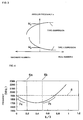
- the type I is one of general forms of the dispersion relation k ( ⁇ ) depicted in Fig. 3 .
- the vertical axis represents the angular frequency ⁇ .
- the horizontal axis on the right side of the vertical axis represents real values of wave number k.
- the wave number is imaginary.
- the wave number k is real when the angular frequency ⁇ is above the cut-off angular frequency ⁇ c of the plate.
- Patent Document 1 PCT Japanese Translation Patent Publication No. 2003-505906
- Fig. 3 only a small-wave-number (long-wavelength) region is calculated.
- a dispersion curve determined by more detailed calculation is shown in Fig. 4 .
- the vertical axis represents the frequency.
- the horizontal axis represents b/ ⁇ obtained by normalizing the thickness b of the piezoelectric film by the wavelength ⁇ of the wave propagating in a planar direction. That is, Fig. 4 shows the dispersion curve of the real wave number part.
- Reference numeral 6a represents the case of a wavelength that is about five times the thickness of the piezoelectric film.
- Reference numeral 6b represents the case of a wavelength that is about twice the thickness of the piezoelectric film.
- Reference numeral 8 represents a resonant frequency. The graph demonstrates that long-wavelength Lamb waves 7a and short-wavelength Lamb waves 7b are both present at frequencies near the resonant frequency.
- a reduction in the thickness of the cross section of a frame-like zone at the edge of the vibrating region eliminates the generation of a long-wavelength spurious mode in a region where the wavelength represented by reference numeral 7a is about five or more times the thickness of the piezoelectric film in Fig. 4 .
- a short-wavelength spurious mode is present in a region where the wavelength represented by reference numeral 7b is equal to or less than about twice the thickness of the piezoelectric film in Fig. 4 in addition to the long-wavelength spurious mode.
- the short-wavelength spurious mode can be suppressed by forming the planar shape of the resonator into a free form as shown in Fig. 1 .
- the resonator having the shape is difficult to arrange and is not suitable for the miniaturization of the piezoelectric resonator.
- the planar shape of the resonator also affects the layout of a filter and the size of a chip; hence, a substantially rectangular shape is preferred.
- the present invention provides a piezoelectric resonator having a structure described below.
- the piezoelectric resonator includes a substrate; a pair of conductive layers disposed on the substrate; and a piezoelectric layer disposed between the pair of conductive layers. At least a region of the piezoelectric layer disposed between the pair of conductive layers (hereinafter, the region being referred to as a "vibrating region”) is acoustically isolated from the substrate.
- the region being referred to as a "vibrating region”
- the vibrating region has a real wave number.
- the shape of the vibrating region when viewed in the thickness direction of the pair of conductive layers and the piezoelectric layer (hereinafter, the shape being referred to as a "planar shape") is a substantial polygon, sides of the substantial polygon are not parallel to each other.
- the vibrating region includes a peripheral portion extending along outer edges of the planar shape and having a relatively small thickness; and a central portion extending inside the peripheral portion and having a relatively large thickness.
- the vibrating region is acoustically isolated by a gap or a sound reflecting layer provided between the vibrating region and the substrate or by an opening formed in the substrate.
- the planar shape of the vibrating region is a polygon in which sides thereof are not parallel to each other. Every time a wave generated in the vibrating region is reflected from the outer edges of the vibrating region, the direction of propagation is different. Thus, the reflected waves cancel each other out by scattering as a whole, thereby eliminating the generation of an undesired component due to interference. This suppresses waves having relatively short wavelengths to improve spurious characteristics in a resonant frequency or less.
- the peripheral portion of the vibrating region has a thickness smaller than that of the central portion; hence, a step is present.
- the step suppresses waves having relatively long wavelength to improve spurious characteristics between the resonant frequency and an anti-resonant frequency.
- the present invention provides a piezoelectric resonator having a structure described below.
- a piezoelectric resonator includes a substrate; a pair of conductive layers; and a piezoelectric layer disposed between the pair of conductive layers. At least a region of the piezoelectric layer disposed between the pair of conductive layers (hereinafter, the region being referred to as a "vibrating region”) is acoustically isolated from the substrate.
- the region being referred to as a "vibrating region"
- the vibrating region has a real wave number.
- the shape of the vibrating region when viewed in the thickness direction of the pair of conductive layers and the piezoelectric layer (hereinafter, the shape being referred to as a "planar shape") is a substantial rectangle, sides of the substantial rectangle each have a waveform in which a curved or angular wave segment is repeated.
- the vibrating region includes a peripheral portion extending along outer edges of the planar shape and having a relatively small thickness; and a central portion extending inside the peripheral portion and having a relatively large thickness.
- the vibrating region is acoustically isolated by a gap or a sound reflecting layer provided between the vibrating region and the substrate or by an opening formed in the substrate.
- outer edges of the planar shape of the vibrating region each have a waveform.
- a wave generated in the vibrating region is reflected in various directions.
- the reflected waves cancel each other out by scattering as a whole, thereby eliminating the generation of an undesired component due to interference.
- the peripheral portion of the vibrating region has a thickness smaller than that of the central portion; hence, a step is present.
- the step suppresses waves having relatively long wavelength to improve spurious characteristics in a resonant frequency or less.
- planar shape of the vibrating region is a substantially rectangle, thereby facilitating layout and reducing the size of the piezoelectric resonator.
- the piezoelectric resonator having any one of the above-described structure further includes a dielectric layer extending along at least one conductive layer of the pair of conductive layers, the dielectric layer being disposed on a side of the at least one conductive layer opposite the side adjacent to the piezoelectric layer.
- the dielectric layer is arranged so as to be superposed at least on the vibrating region when viewed in the thickness direction of the pair of conductive layers and the piezoelectric layer.
- the dielectric layer arranged so as to be superposed at least on the vibrating region when viewed in the thickness direction of the pair of conductive layers and the piezoelectric layer vibrates together with the piezoelectric layer and the pair of conductive layers of the vibrating region.
- the presence of the dielectric layer facilitates control of the frequency of the piezoelectric resonator.
- the planar shape of the vibrating region suppresses a spurious Lamb wave having a relatively short wavelength that is equal to or less than twice the thickness of the piezoelectric layer, and the thicknesses of the peripheral portion and the central portion suppress a spurious Lamb wave having a relatively long wavelength that is five or more times the thickness of the piezoelectric layer.
- the spurious waves are suppressed by different methods in response to the wavelength, thereby improving total characteristics.
- each of the outer edges of the vibrating region with a substantially rectangular planar shape has a) at least one waveform selected from a triangular wave, a rectangular wave, a sinusoidal wave, and an irregular wave or has b) a waveform obtained by combining two or more waves selected from a triangular wave, a rectangular wave, a sinusoidal wave, and an irregular wave.
- the outer edges each having the waveform provides spurious-modesuppressed resonance characteristics.
- the vibrating region has a substantially rectangular planar shape.
- Each of the outer edges of the planar shape has a waveform in which a single wave segment having a length of 0.5 to 12.5 times the thickness of the piezoelectric layer is repeated.
- the outer edges each having the waveform provides short-wavelength-spurious-mode resonance characteristics.
- the planar shape is a rectangle, thereby facilitating layout and reducing the size of the piezoelectric resonator.
- the vibrating region has a substantially rectangular planar shape.
- Each of the outer edges of the planar shape has a waveform in which a single wave segment having a total amplitude of 0.5 to 6.25 times the thickness of the piezoelectric layer is repeated.
- the outer edges each having the waveform provides short-wavelength-spurious-mode resonance characteristics.
- the planar shape is a rectangle, thereby facilitating layout and reducing the size of the piezoelectric resonator.
- At least one of the pair of conductive layers has a relatively small thickness at a portion included in the peripheral portion of the vibrating region and has a relatively large thickness at a portion included in the central portion of the vibrating region.
- the central portion of the vibrating region has a thickness larger than that of the peripheral portion of the vibrating region by the formation of a step of the conductive layer. This suppresses long-wavelength spurious modes.
- the piezoelectric layer has a relatively small thickness at a portion included in the peripheral portion of the vibrating region and has a relatively large thickness at a portion included in the central portion of the vibrating region.
- the central portion of the vibrating region has a thickness larger than that of the peripheral portion of the vibrating region by the formation of a step of the piezoelectric layer. This suppresses long-wavelength spurious modes.
- the dielectric layer has a relatively small thickness at a portion included in the peripheral portion of the vibrating region and has a relatively large thickness at a portion included in the central portion of the vibrating region.
- the central portion of the vibrating region has a thickness larger than that of the peripheral portion of the vibrating region by the formation of a step of the dielectric layer. This suppresses long-wavelength spurious modes.
- the peripheral portion of the vibrating region has a tapered profile with a gradual change in thickness in the vicinity of the boundary between the peripheral portion and the central portion of the vibrating region.
- the step of the vibrating region is easily formed by etching or the like.
- the vibrating region has a step profile having a sharp change in thickness at the boundary between the peripheral portion and the central portion of the vibrating region.
- the width of the step formed in the vibrating region is accurately controlled.
- the width of the peripheral portion of the vibrating region is 3 to 9 times the thickness of the piezoelectric layer.
- the above-described structure provides long-wavelength-spurious-mode-suppressed resonance characteristics.
- At least one conductive layer of the pair of conductive layers includes at least two sublayers stacked.
- one sublayer of the at least two sublayers is located adjacent to the piezoelectric layer, and the other sublayer of the at least two sublayers is located remote from the piezoelectric layer and is arranged inside and apart from an end of the one sublayer in the vibrating region.
- At least one of the pair of conductive layers includes at least two sublayers stacked, the at least two sublayers having different etching resistances.
- the other sublayer is arranged inside and apart from an end of the one sublayer by etching an end portion of the other sublayer until the one sublayer is exposed.
- the one sublayer having a relatively high etching resistance contains at least one metal selected from the group consisting of Pt, W, Mo, Ir, Os, Re, and Ru.
- the other sublayer having a relatively low etching resistance contains at least one metal selected from the group consisting of Al, Ti, Au, NiCr, Cr, and Cu.
- the piezoelectric material constituting the piezoelectric layer is AlN or ZnO.
- the above-described structure provides long-wavelength-spurious-mode-suppressed resonance characteristics.
- the dielectric layer is composed of at least one dielectric material selected from the group consisting of SiO 2 , AlN, and SiN.
- the above-described structure provides long-wavelength-spurious-mode-suppressed resonance characteristics.
- the present invention provides a piezoelectric thin-film filter having a structure described below.
- the piezoelectric thin-film filter includes a plurality of piezoelectric resonators. Only some of the plurality of piezoelectric resonators are the piezoelectric resonators having any of the above-described structures.
- the above-described structure provides satisfactory ripple-suppressed filter characteristics while the pass band width of the filter is ensured.
- the present invention provides a piezoelectric thin-film filter having a structure described below.
- the piezoelectric thin-film filter includes a plurality of piezoelectric resonators connected in the form of a ladder. One or more of the piezoelectric resonators are connected in series, and at least one of the series-connected piezoelectric resonators is the piezoelectric resonator having any of the structures described above.
- the above-described structure provides satisfactory ripple-suppressed filter characteristics while the pass band width of the filter is ensured.
- the present invention provides a piezoelectric thin-film filter having a structure described below.
- the piezoelectric thin-film filter includes a plurality of piezoelectric resonators connected in the form of a ladder. At least one relatively-high-frequency piezoelectric resonator of the plurality of piezoelectric resonators is the piezoelectric resonator having any of the structures described above.
- the above-described structure provides satisfactory ripple-suppressed filter characteristics while the pass band width of the filter is ensured.
- the piezoelectric resonator and the piezoelectric thin-film filter of the present invention can suppress long-wavelength spurious modes and short-wavelength spurious modes.
- a piezoelectric resonator including at least two conductive layers and at least one piezoelectric layer disposed between the conductive layers and a piezoelectric thin-film filter configured by a combination of the piezoelectric resonators
- advantages (1) to (4) as follows:
- the edges having the waveform of the rectangular vibrating region scatter a wave having a wavelength comparable to the waveform at the edges to cancel a spurious wave (short-wavelength spurious wave) out.
- An increase in the scale of the waveform cancels a long-wavelength wave out.
- the formation of steps at the edges of the vibrating region as described in Item (1) provides more satisfactory characteristics, facilitates layout, and reduces the size of the resonator.
- a resonator having steps at edges of a vibrating region and having a waveform at the edges of the vibrating region was actually formed by the techniques described in Items (1) and (2).
- Smith charts in Figs. 5(a) and 5(b) it was found that characteristics at a resonant frequency or less were improved but that characteristics at the resonant frequency or more were degraded.
- Symbol s represents the case where the steps are formed at the edges of the rectangular vibrating region having sides that are not parallel to each other.
- Symbol t represents the case where no step is formed at the edges of the rectangular vibrating region having sides that are not parallel to each other.
- Fig. 5(b) is an enlarged view of a portion indicated by Symbol A in Fig. 5(a) .
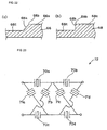
- resonators 80a to 80d may be connected in the form of a lattice to form a filter.
- resonators 83 and 84 may be connected in the form of a ladder to form a filter.
- Fig. 7 shows the relationship of characteristics of a resonator and a lattice filter formed by combining resonators (series resonator and parallel resonator) having different frequencies.
- a resonator having a relatively high frequency is used as the series resonator.
- reference numeral 80 represents the impedance of the series resonator.
- Reference numeral 81 represents the impedance of the parallel resonator.
- Reference numeral 82 represents filter characteristics.
- the characteristics in the pass band width P of the filter are affected by characteristics of the series resonator at and near the resonant frequency and the parallel resonator at and near the anti-resonant frequency.
- the parallel resonator impairs the characteristics in the pass band width of the filter.
- Symbol a represents filter characteristics when the technique described in Item (2) is employed for both of the series resonator and parallel resonator.
- Symbol b represents filter characteristics when the technique described in Item (2) is employed for only the series resonator.
- Symbol c represents filter characteristics when the technique described in Item (2) is not employed for any of the series resonator and parallel resonator.
- the piezoelectric resonator 10 includes a bottom electrode 14, a piezoelectric layer 15, a top electrode 16, and a dielectric film 17 stacked in that order on a substrate 12.
- the bottom electrode 14 has a portion supported by the substrate 12 and a floating portion remote from the substrate 12 with a gap 13.
- the vibrating region 18 is a portion in which the bottom electrode 14 and the top electrode 16 overlap one another when viewed in the thickness direction (the direction perpendicular to the paper plane in Fig. 9(b) ).
- the vibrating region 18 is acoustically isolated from the substrate 12 via the gap 13.
- a sound reflecting layer may be disposed between the substrate 12 and the vibrating region 18 to acoustically isolate the vibrating region 18 from the substrate 12.
- the vibrating region 18 includes a peripheral portion 18t extending along outer edges 18a of the vibrating region 18; and a central portion 18s extending inside the peripheral portion 18t, when viewed in the thickness direction.
- the boundary 18k between the peripheral portion 18t and the central portion 18s of the vibrating region 18 is represented by a broken line.
- the shape of the outer edges 18a of the vibrating region 18 is a substantial rectangle when viewed in the thickness direction. Sides of the substantial rectangle each have a waveform. That is, an end 14a of the bottom electrode 14, an end 16a of the top electrode 16, portions 16s and 16t of both sides adjacent to both ends, which constitute the outer edges 18a of the vibrating region 18, each have a waveform in which a triangular wave segment is repeated.
- Outer edges 18a of the vibrating region 18 may have a waveform.
- a rectangular waveform may be used as in outer edges 18b of a vibrating region 18x shown in Fig. 10 that is a fragmentary plan view.
- a sinusoidal waveform may be used.
- the waveform of the outer edges 18a may have an irregular period and irregular amplitude.
- the boundary 18k' between a peripheral portion 18t' and a central portion 18s' of the vibrating region 18x is represented by a broken line.
- the bottom electrode 14, the piezoelectric layer 15, and the top electrode 16 each have a substantially constant thickness.
- a portion constituting the central portion 18s of the vibrating region 18 has a thickness larger than that of the remainder.
- the peripheral portion 18t has a thickness smaller than that of the central portion 18s, thereby forming a step in the vibrating region 18.
- a portion not including the step may be present.
- the vibrating region 18 has the type II dispersion property shown in Fig. 4 .
- the dielectric film 17 composed of SiO 2 is formed on the piezoelectric layer 15 composed of AlN.
- the width W of the dielectric film 17 at the peripheral portion 18t of the vibrating region 18 is set at about 10 ⁇ m.
- a change in thickness ⁇ t due to the step is set at about 20 nm.
- the shape of the outer edges 18a of the vibrating region 18 is the substantial rectangle, and each of the sides of the substantial rectangle has the triangular waveform; hence, the piezoelectric resonator 10 can suppress short-wavelength spurious modes. This is probably because among waves reflected from the outer edges 18a of the vibrating region 18, wave components having wavelengths corresponding to the shape of the outer edges 18a cancel each other out, thereby eliminating the generation of an undesired component due to interference.
- the shape of outer edges 18c of a vibrating region 18y is a substantial rectangle, and sides of the substantial rectangle each have an irregular waveform.
- the boundary 18k " between a peripheral portion 18t" and a central portion 18s" of the vibrating region 18y is represented by a broken line.
- short-wavelength spurious modes can be suppressed. This is probably because waves reflected from the outer edges 18c cancel each other out by scattering, thereby eliminating the generation of an undesired component due to interference.
- the peripheral portion 18t" of the vibrating region 18y has a thickness smaller than that of the central portion 18s'', as in the first embodiment, thereby suppressing long-wavelength spurious modes.
- a vibrating region 28 is acoustically isolated from a substrate 22 with a gap 23, as in the first embodiment.
- a portion constituting a central portion 28s of the vibrating region 28 has a thickness larger than that of the remainder.
- a bottom electrode 24, a piezoelectric layer 25, and a dielectric layer 27 each have a substantially constant thickness.
- a peripheral portion 28t of the vibrating region has a thickness smaller than that of the central portion 28s, thereby forming a step in the vibrating region 28.
- the dielectric layer 27 composed of SiO 2 is formed on the piezoelectric layer 25 composed of AlN.
- the width W of a portion 26a of the top electrode 26, which is the peripheral portion 28t of the vibrating region 28 is set at about 10 ⁇ m.
- a change in thickness ⁇ t is set at about 5 nm.
- the planar shape of the vibrating region 28 is a rectangle. Outer edges of the vibrating region 28 each have a waveform.
- a drawing is the same as Fig. 9(b) in the first embodiment and is thus omitted.
- the piezoelectric resonator 20 can suppress both long-wavelength spurious modes and short-wavelength spurious modes as in the first embodiment.
- a vibrating region 38 is acoustically isolated from a substrate 32 with a gap 33, as in the first embodiment.
- a portion 34a constituting a central portion 38s of the vibrating region 38 has a thickness larger than that of the remainder.
- a bottom electrode 34, a top electrode 36, and a dielectric layer 37 each have a substantially constant thickness.
- a peripheral portion 38t of the vibrating region 38 has a thickness smaller than that of the central portion 38s, thereby forming a step in the vibrating region 38.
- the dielectric layer 37 composed of SiO 2 is formed on the piezoelectric layer 35 composed of AlN.
- the width W of the step on the piezoelectric layer 35 is set at about 10 ⁇ m.
- a change in thickness ⁇ t is set at about 20 nm.
- the planar shape of the vibrating region 38 is a rectangle. Outer edges of the vibrating region 38 each have a waveform.
- a drawing is the same as Fig. 9(b) in the first embodiment and is thus omitted.
- the piezoelectric resonator 30 can suppress both long-wavelength spurious modes and short-wavelength spurious modes as in the first embodiment.
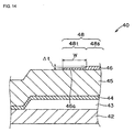
- the piezoelectric resonator 40 does not include a dielectric layer. That is, a vibrating region 48 acoustically isolated from a substrate 42 with a gap 43 includes a bottom electrode 44, a piezoelectric layer 45, and a top electrode 46.
- a portion constituting a central portion 48s of the vibrating region 48 has a thickness larger than that of the remainder.
- the bottom electrode 44 and the piezoelectric layer 45 each have a substantially constant thickness.
- a peripheral portion 48t of the vibrating region 48 has a thickness smaller than that of the central portion 48s, thereby forming a step in the vibrating region 48.
- the step is formed on the top electrode 46 disposed on the piezoelectric layer 45 composed of AlN.
- the width W of the step is set at about 10 ⁇ m.
- a change in thickness ⁇ t is set at about 5 nm.
- the planar shape of the vibrating region 48 is a rectangle. Outer edges of the vibrating region 48 each have a waveform.
- a drawing is the same as Fig. 9(b) in the first embodiment and is thus omitted.
- the piezoelectric resonator 40 can suppress both long-wavelength spurious modes and short-wavelength spurious modes as in the first embodiment.
- the piezoelectric resonator 50 does not include a dielectric layer. That is, a vibrating region 58 acoustically isolated from a substrate 52 with a gap 53 includes a bottom electrode 54, a piezoelectric layer 55, and a top electrode 56.
- a portion constituting a central portion 58s of the vibrating region 58 has larger than that of the remainder.
- the bottom electrode 54 and the top electrode 56 each have a substantially constant thickness.
- a peripheral portion 58t of the vibrating region 58 has a thickness smaller than that of the central portion 58s, thereby forming a step in the vibrating region 58.
- the step is formed on the piezoelectric layer 45 composed of AlN.
- the width W of the step is set at about 10 ⁇ m.
- a change in thickness ⁇ t is set at about 20 nm.
- the planar shape of the vibrating region 58 is a rectangle. Outer edges of the vibrating region 58 each have a waveform.
- a drawing is the same as Fig. 9(b) in the first embodiment and is thus omitted.
- the piezoelectric resonator 50 can suppress both long-wavelength spurious modes and short-wavelength spurious modes as in the first embodiment.
- a vibrating region is acoustically isolated from a substrate with a gap, as in the first embodiment.
- a bottom electrode, a piezoelectric layer, a top electrode, and a dielectric layer that constitute the vibrating region each have a substantially constant thickness.
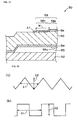
- the planar shape of outer edges of the vibrating region is a substantial rectangle as in the first embodiment. Sides of the substantially rectangular planar shape of the outer edges of the vibrating region each have a triangular waveform shown in Fig. 16(a) or a rectangular waveform shown in Fig. 16(b) . As shown in Fig. 16(a) and 16(b) , let the length and total amplitude of the triangular or rectangular wave per period (wavelength) be ⁇ 1 and ⁇ 2, respectively. Characteristics of the resonator are changed depending on ⁇ 1 and ⁇ 2.
- the outer edges of the vibrating region each have the waveform. They scatter waves comparable to the waveform of the outer edges of the vibrating region to eliminate spurious waves.
- the length of the waveform of the outer edges of the vibrating region may be 1/4 or more times a wavelength to be suppressed.
- Each of ⁇ 1 and ⁇ 2 may be 0.5 or more times the thickness of the piezoelectric layer. Experiments demonstrated that each of ⁇ 1 and ⁇ 2 has an upper limit.
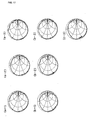
- Figs. 17(a-1) to 17(c-3) show that when ⁇ 1 ⁇ 20 ⁇ m and ⁇ 2 ⁇ 10 ⁇ m, short-wavelength spurious modes are suppressed.
- the upper limit of ⁇ 2 is 6.25 times the piezoelectric layer (10/1.6).
- W 0 ( ⁇ m), i.e., a step is absent on the vibrating region.
- W 5 ( ⁇ m).
- W 10 ( ⁇ m).
- W 15 ( ⁇ m).
- W 20 ( ⁇ m) .
- Figs. 18(a) to 18(e) show that when the step width W is in the range of 5 ⁇ W ⁇ 15, long-wavelength spurious modes are suppressed.
- the results demonstrate that the lower limit of the step width W is about three times the thickness of the piezoelectric layer.
- the upper limit of the step width W is about is about nine times the thickness of the piezoelectric layer.
- ⁇ t 0 (i.e., a step is absent).
- Fig. 19(b) 20 (nm).
- Figs. 19(a) to 19(d) show that when the change in the thickness ⁇ t of the step is in the range of 0 ⁇ ⁇ t ⁇ 30, long-wavelength spurious modes are suppressed.
- the steps are formed by etching.
- a top electrode 60 includes at least one layer 64 having a low etching resistance, the at least one layer 64 being composed of A1, Au, or the like and located as the uppermost layer; and at least one layer 62 having a high etching resistance, the at least one layer 62 being composed of Pt or the like and located below the at least one layer 64.
- the top electrode 60 having a step may be formed by a procedure shown in Figs. 21(a) to 21(d) .
- the layer 64 having a low etching resistance and composed of Al, Au, or the like is formed on the layer 62 having a high etching resistance and composed of Pt or the like.
- an etching mask is formed with a resist 65.
- the layer 64 having a low etching resistance is completely removed by etching with the mask.
- the resist 65 is removed.
- Examples of a material usable for the layer 62 having a relatively high etching resistance include metals, such as W, Mo, Ir, Os, Re, and Ru, as well as Pt.
- Examples of a material usable for the layer 64 having a relatively low etching resistance include metals, such as Ti, NiCr, Cr, and Cu, as well as Al and Au. Two or more metals may be used for each of the layers 62 and 64.
- top electrode including the two layers having different etching resistances facilitates formation of the step on the vibrating region.
- an inclined surface 66k is formed in the vicinity of the boundary 66b between a central portion 66s and a peripheral portion 66t of a vibrating region 66 to form a tapered profile with a gradual change in the thickness of the vibrating region 66. Thereby, a step is formed on the vibrating region 66.
- a substantially vertical surface 68k is formed in the vicinity of the boundary 68b between a central portion 68s and a peripheral portion 68t of a vibrating region 68 to form a step profile having a sharp change in the thickness of the vibrating region 68.
- a step is formed on the vibrating region 68.
- a lattice filter 72 is configured by connecting series resonators 70a to 70d and parallel resonators 71a to 71d in the form of a lattice.
- Fig. 23 shows the case where the number of poles is two. The number of poles may be one or three or more.
- each of the series resonators 70a to 70d each having a relatively high frequency has a structure capable of suppressing long-wavelength spurious modes. That is, only each of the series resonators 70a to 70d each having a relatively high frequency has a step along outer edges of a vibrating region.
- Fig. 24 shows exemplary characteristics of the lattice filter 72.
- Reference numeral 70s represents impedance characteristics when the series resonators 70a to 70d have the same characteristic.
- Reference numeral 71s represents impedance characteristics when the parallel resonators 71a to 71d have the same characteristic.
- Reference numeral 72s represents filter characteristics of the lattice filter 72 including the series resonators 70a to 70d having the impedance characteristics represented by reference numeral 70s and the parallel resonators 71a to 71d having the impedance characteristics represented by reference numeral 71s.
- the lattice filter 72 has satisfactory spurious characteristics with ripples suppressed in the pass band width of the filter.
- the ladder filter 76 is configured by connecting series resonators 74a and 74b and parallel resonators 75a and 75b in the form of a ladder.
- Fig. 25 shows the case where the number of poles is two. The number of poles may be one or three or more.
- each of the series resonators 74a to 74b has a structure capable of suppressing long-wavelength spurious modes. That is, only each of the series resonators 74a to 74b has a step along outer edges of a vibrating region, wherein a peripheral portion of the vibrating region has a thickness smaller than that of a central portion of the vibrating region.
- Fig. 26 shows exemplary characteristics of the ladder filter 76.
- Reference numeral 74s represents impedance characteristics when the series resonators 74a and 74b have the same characteristic.
- Reference numeral 75s represents impedance characteristics when the parallel resonators 75a and 75b have the same characteristic.
- Reference numeral 76s represents filter characteristics of the ladder filter 76 including the series resonators 74a and 74b having the impedance characteristics represented by reference numeral 74s and the parallel resonators 75a and 75b having the impedance characteristics represented by reference numeral 75s.
- the ladder filter 76 has satisfactory spurious characteristics with ripples suppressed in the pass band width of the filter.
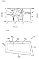
- the planar shape of a vibrating region 78 of the piezoelectric resonator according to the fourteenth embodiment is a rectangle with sides that are not parallel to each other.
- Each of sides 78a to 78d of the rectangular planar shape of the vibrating region 78 does not have a waveform but is straight.
- the peripheral portion 78t of the vibrating region 78 has a thickness smaller than that of a central portion 78s of the vibrating region 78.
- the boundary 78k between the central portion 78s and the peripheral portion 78t of the vibrating region 78 is represented by a broken line.
- the piezoelectric resonator according to the fourteenth embodiment reduces long-wavelength spurious modes.
- a step is formed on the vibrating region 78 by changing a dielectric layer composed of SiO 2 .
- the characteristics of the piezoelectric resonator in which the width of the step on the vibrating region 78 is 10 ⁇ m and in which a change in the thickness of the step is 20 nm are the same as that represented by Symbol s in Figs. 5(a) and 5(b) .
- a resonator having a shape that facilitates layout and having suppressed long-wavelength spurious modes and short-wavelength spurious modes.
- a filter having satisfactory ripple-suppressed filter characteristics while the pass band width of the filter is ensured.
- the vibrating region may be acoustically isolated from the substrate by a sound reflecting layer disposed between the substrate and the vibrating region or an opening formed in the substrate.
- the piezoelectric layer may be composed of ZnO having type II dispersion characteristics.
- the dielectric layer may be composed of AlN, SiN, or the like in place of SiO 2 .
- the step on the vibrating region may be formed by changing the thicknesses of two or more of the conductive layer, the piezoelectric layer, and the dielectric layer.
- the piezoelectric resonator may have a structure without the dielectric layer.
Landscapes
- Physics & Mathematics (AREA)
- Acoustics & Sound (AREA)
- Piezo-Electric Or Mechanical Vibrators, Or Delay Or Filter Circuits (AREA)
Abstract
Description
- The present invention relates to piezoelectric resonators and piezoelectric thin-film filters. Specifically, the present invention relates to a piezoelectric resonator in which a vibrating region including a pair of conductive layers with a piezoelectric layer provided therebetween is supported so as to be acoustically isolated from a substrate and a piezoelectric thin-film filter including the piezoelectric resonator.
- In piezoelectric resonators in which piezoelectric resonator elements each including a pair of electrode films with a piezoelectric film are supported on substrates so as to be acoustically isolated from the substrates and operating in a thickness-extensional vibration mode, a transverse vibration mode generates waves that propagate in a planar direction when piezoelectric resonator elements vibrate in the thickness direction, causing the generation of a spurious wave.
- To suppress such a spurious wave, for example, as shown in
Figs. 1 and 2 , a piezoelectric resonator is reported to have a free-form vibrating region and a bump along the periphery of the vibrating region. That is, abottom electrode 110 and apiezoelectric layer 100 are each disposed on a SiO2 support layer 200 serving as a substrate and each extend across the full width of the resonator.Boundary regions central portion 3 of aresonator structure 1000 are covered with atop electrode 120. Theboundary regions resonator structure 1000 are formed by increasing the thickness of thetop electrode layer 120 on the periphery of the electrically excitable vibrating region. Thecentral portion 3 of aresonator 1200 has a free form. Arrows inFig. 2 indicate scale. The scale in the horizontal direction differs from that in the vertical direction. - In the case where the bump is formed between the free-form
central portion 3 and theboundary regions - The reason for the edge (boundary regions) of the vibrating region having a thickness larger than that of the central region is that the ZnO exhibiting the dispersion property of type I is used. The type I is one of general forms of the dispersion relation k (ω) depicted in
Fig. 3 . InFig. 3 , the vertical axis represents the angular frequency ω. The horizontal axis on the right side of the vertical axis represents real values of wave number k. On the left side of the vertical axis, the wave number is imaginary. In type I dispersion, the wave number k is real when the angular frequency ω is above the cut-off angular frequency ωc of the plate. In type II dispersion, the wave number k is real when the angular frequency ω is below the cut-off angular frequency ωc of the plate (for example, Patent Document 1).
Patent Document 1:PCT Japanese Translation Patent Publication No. 2003-505906 - In
Fig. 3 , only a small-wave-number (long-wavelength) region is calculated. In a structure including a piezoelectric film having the type II dispersion property depicted inFig. 3 , for example, a dispersion curve determined by more detailed calculation is shown inFig. 4 . InFig. 4 , the vertical axis represents the frequency. The horizontal axis represents b/λ obtained by normalizing the thickness b of the piezoelectric film by the wavelength λ of the wave propagating in a planar direction. That is,Fig. 4 shows the dispersion curve of the real wave number part.Reference numeral 6a represents the case of a wavelength that is about five times the thickness of the piezoelectric film.Reference numeral 6b represents the case of a wavelength that is about twice the thickness of the piezoelectric film.Reference numeral 8 represents a resonant frequency. The graph demonstrates that long-wavelength Lamb waves 7a and short-wavelength Lamb waves 7b are both present at frequencies near the resonant frequency. - A reduction in the thickness of the cross section of a frame-like zone at the edge of the vibrating region eliminates the generation of a long-wavelength spurious mode in a region where the wavelength represented by
reference numeral 7a is about five or more times the thickness of the piezoelectric film inFig. 4 . In the case of the dispersion curve as shown inFig. 4 , however, in the vicinity of theresonant frequency 8, a short-wavelength spurious mode is present in a region where the wavelength represented byreference numeral 7b is equal to or less than about twice the thickness of the piezoelectric film inFig. 4 in addition to the long-wavelength spurious mode. - The short-wavelength spurious mode can be suppressed by forming the planar shape of the resonator into a free form as shown in
Fig. 1 . However, the resonator having the shape is difficult to arrange and is not suitable for the miniaturization of the piezoelectric resonator. The planar shape of the resonator also affects the layout of a filter and the size of a chip; hence, a substantially rectangular shape is preferred. - The origin of the short-wavelength spurious radiation is insufficiently analyzed. Thus, an optimum planar shape of the vibrating region is not found.
- In consideration of the above-described situation, it is an object of the present invention to provide a piezoelectric resonator capable of suppressing the long-wavelength spurious mode and the short-wavelength spurious mode and provide a piezoelectric thin-film filter including the piezoelectric resonator.
- To overcome the foregoing problems, the present invention provides a piezoelectric resonator having a structure described below.
- The piezoelectric resonator includes a substrate; a pair of conductive layers disposed on the substrate; and a piezoelectric layer disposed between the pair of conductive layers. At least a region of the piezoelectric layer disposed between the pair of conductive layers (hereinafter, the region being referred to as a "vibrating region") is acoustically isolated from the substrate. In a dispersion curve in which the vertical axis represents the frequency, the horizontal axis on the right side of the vertical axis represents the real wave number, and the horizontal axis on the left side of the vertical axis represents the imaginary wave number, when the frequency is lower than a cut-off angular frequency ωc, the vibrating region has a real wave number. The shape of the vibrating region when viewed in the thickness direction of the pair of conductive layers and the piezoelectric layer (hereinafter, the shape being referred to as a "planar shape") is a substantial polygon, sides of the substantial polygon are not parallel to each other. The vibrating region includes a peripheral portion extending along outer edges of the planar shape and having a relatively small thickness; and a central portion extending inside the peripheral portion and having a relatively large thickness.
- In the above-described structure, the vibrating region is acoustically isolated by a gap or a sound reflecting layer provided between the vibrating region and the substrate or by an opening formed in the substrate.
- According to the above-described structure, the planar shape of the vibrating region is a polygon in which sides thereof are not parallel to each other. Every time a wave generated in the vibrating region is reflected from the outer edges of the vibrating region, the direction of propagation is different. Thus, the reflected waves cancel each other out by scattering as a whole, thereby eliminating the generation of an undesired component due to interference. This suppresses waves having relatively short wavelengths to improve spurious characteristics in a resonant frequency or less.
- The peripheral portion of the vibrating region has a thickness smaller than that of the central portion; hence, a step is present. The step suppresses waves having relatively long wavelength to improve spurious characteristics between the resonant frequency and an anti-resonant frequency.
- Furthermore, to overcome the above-described problems, the present invention provides a piezoelectric resonator having a structure described below.
- A piezoelectric resonator includes a substrate; a pair of conductive layers; and a piezoelectric layer disposed between the pair of conductive layers. At least a region of the piezoelectric layer disposed between the pair of conductive layers (hereinafter, the region being referred to as a "vibrating region") is acoustically isolated from the substrate. In a dispersion curve in which the vertical axis represents the frequency, the horizontal axis on the right side of the vertical axis represents the real wave number, and the horizontal axis on the left side of the vertical axis represents the imaginary wave number, when the frequency is lower than a cut-off angular frequency ωc, the vibrating region has a real wave number. The shape of the vibrating region when viewed in the thickness direction of the pair of conductive layers and the piezoelectric layer (hereinafter, the shape being referred to as a "planar shape") is a substantial rectangle, sides of the substantial rectangle each have a waveform in which a curved or angular wave segment is repeated. The vibrating region includes a peripheral portion extending along outer edges of the planar shape and having a relatively small thickness; and a central portion extending inside the peripheral portion and having a relatively large thickness.
- In the above-described structure, the vibrating region is acoustically isolated by a gap or a sound reflecting layer provided between the vibrating region and the substrate or by an opening formed in the substrate.
- According to the above-described structure, outer edges of the planar shape of the vibrating region each have a waveform. A wave generated in the vibrating region is reflected in various directions. Thus, the reflected waves cancel each other out by scattering as a whole, thereby eliminating the generation of an undesired component due to interference. This suppresses waves having relatively short wavelengths to improve spurious characteristics between a resonant frequency and an anti-resonant frequency.
- The peripheral portion of the vibrating region has a thickness smaller than that of the central portion; hence, a step is present. The step suppresses waves having relatively long wavelength to improve spurious characteristics in a resonant frequency or less.
- Furthermore, the planar shape of the vibrating region is a substantially rectangle, thereby facilitating layout and reducing the size of the piezoelectric resonator.
- Preferably, the piezoelectric resonator having any one of the above-described structure further includes a dielectric layer extending along at least one conductive layer of the pair of conductive layers, the dielectric layer being disposed on a side of the at least one conductive layer opposite the side adjacent to the piezoelectric layer. The dielectric layer is arranged so as to be superposed at least on the vibrating region when viewed in the thickness direction of the pair of conductive layers and the piezoelectric layer.
- In the above-described structure, the dielectric layer arranged so as to be superposed at least on the vibrating region when viewed in the thickness direction of the pair of conductive layers and the piezoelectric layer vibrates together with the piezoelectric layer and the pair of conductive layers of the vibrating region.
- According to the above-described structure, the presence of the dielectric layer facilitates control of the frequency of the piezoelectric resonator.
- Preferably, the planar shape of the vibrating region suppresses a spurious Lamb wave having a relatively short wavelength that is equal to or less than twice the thickness of the piezoelectric layer, and the thicknesses of the peripheral portion and the central portion suppress a spurious Lamb wave having a relatively long wavelength that is five or more times the thickness of the piezoelectric layer.
- According to the above-described structure, the spurious waves are suppressed by different methods in response to the wavelength, thereby improving total characteristics.
- Specifically, various structures can be used as follows.
- Preferably, each of the outer edges of the vibrating region with a substantially rectangular planar shape has a) at least one waveform selected from a triangular wave, a rectangular wave, a sinusoidal wave, and an irregular wave or has b) a waveform obtained by combining two or more waves selected from a triangular wave, a rectangular wave, a sinusoidal wave, and an irregular wave.
- According to the above-described structure, the outer edges each having the waveform provides spurious-modesuppressed resonance characteristics.
- Preferably, the vibrating region has a substantially rectangular planar shape. Each of the outer edges of the planar shape has a waveform in which a single wave segment having a length of 0.5 to 12.5 times the thickness of the piezoelectric layer is repeated.
- According to the above-described structure, the outer edges each having the waveform provides short-wavelength-spurious-mode resonance characteristics. The planar shape is a rectangle, thereby facilitating layout and reducing the size of the piezoelectric resonator.
- Preferably, the vibrating region has a substantially rectangular planar shape. Each of the outer edges of the planar shape has a waveform in which a single wave segment having a total amplitude of 0.5 to 6.25 times the thickness of the piezoelectric layer is repeated.
- According to the above-described structure, the outer edges each having the waveform provides short-wavelength-spurious-mode resonance characteristics. The planar shape is a rectangle, thereby facilitating layout and reducing the size of the piezoelectric resonator.
- Preferably, at least one of the pair of conductive layers has a relatively small thickness at a portion included in the peripheral portion of the vibrating region and has a relatively large thickness at a portion included in the central portion of the vibrating region.
- According to the above-described structure, the central portion of the vibrating region has a thickness larger than that of the peripheral portion of the vibrating region by the formation of a step of the conductive layer. This suppresses long-wavelength spurious modes.
- Preferably, the piezoelectric layer has a relatively small thickness at a portion included in the peripheral portion of the vibrating region and has a relatively large thickness at a portion included in the central portion of the vibrating region.
- According to the above-described structure, the central portion of the vibrating region has a thickness larger than that of the peripheral portion of the vibrating region by the formation of a step of the piezoelectric layer. This suppresses long-wavelength spurious modes.
- Preferably, the dielectric layer has a relatively small thickness at a portion included in the peripheral portion of the vibrating region and has a relatively large thickness at a portion included in the central portion of the vibrating region.
- According to the above-described structure, the central portion of the vibrating region has a thickness larger than that of the peripheral portion of the vibrating region by the formation of a step of the dielectric layer. This suppresses long-wavelength spurious modes.
- Preferably, the peripheral portion of the vibrating region has a tapered profile with a gradual change in thickness in the vicinity of the boundary between the peripheral portion and the central portion of the vibrating region.
- According to the above-described structure, the step of the vibrating region is easily formed by etching or the like.
- Preferably, the vibrating region has a step profile having a sharp change in thickness at the boundary between the peripheral portion and the central portion of the vibrating region.
- According to the above-described structure, the width of the step formed in the vibrating region is accurately controlled.
- Preferably, the width of the peripheral portion of the vibrating region is 3 to 9 times the thickness of the piezoelectric layer.
- The above-described structure provides long-wavelength-spurious-mode-suppressed resonance characteristics.
- Preferably, at least one conductive layer of the pair of conductive layers includes at least two sublayers stacked. one sublayer of the at least two sublayers is located adjacent to the piezoelectric layer, and the other sublayer of the at least two sublayers is located remote from the piezoelectric layer and is arranged inside and apart from an end of the one sublayer in the vibrating region.
- According to the above-described structure, a step that suppresses long-wavelength spurious modes is easily formed.
- Preferably, at least one of the pair of conductive layers includes at least two sublayers stacked, the at least two sublayers having different etching resistances. One sublayer of the at least two sublayers, the one sublayer being located adjacent to the piezoelectric layer, has a relatively high etching resistance. The other sublayer of the at least two sublayers, the other sublayer being located remote from the piezoelectric layer, has a relatively low etching resistance. The other sublayer is arranged inside and apart from an end of the one sublayer by etching an end portion of the other sublayer until the one sublayer is exposed.
- According to the above-described structure, a step that suppresses long-wavelength spurious modes is easily formed.
- Preferably, the one sublayer having a relatively high etching resistance contains at least one metal selected from the group consisting of Pt, W, Mo, Ir, Os, Re, and Ru. The other sublayer having a relatively low etching resistance contains at least one metal selected from the group consisting of Al, Ti, Au, NiCr, Cr, and Cu.
- According to the above-described structure, a step that suppresses long-wavelength spurious modes is easily formed.
- Preferably, the piezoelectric material constituting the piezoelectric layer is AlN or ZnO.
- The above-described structure provides long-wavelength-spurious-mode-suppressed resonance characteristics.
- Preferably, the dielectric layer is composed of at least one dielectric material selected from the group consisting of SiO2, AlN, and SiN.
- The above-described structure provides long-wavelength-spurious-mode-suppressed resonance characteristics.
- Furthermore, to overcome the above-described problems, the present invention provides a piezoelectric thin-film filter having a structure described below.
- The piezoelectric thin-film filter includes a plurality of piezoelectric resonators. Only some of the plurality of piezoelectric resonators are the piezoelectric resonators having any of the above-described structures.
- The above-described structure provides satisfactory ripple-suppressed filter characteristics while the pass band width of the filter is ensured.
- Furthermore, to overcome the above-described problems, the present invention provides a piezoelectric thin-film filter having a structure described below.
- The piezoelectric thin-film filter includes a plurality of piezoelectric resonators connected in the form of a ladder. One or more of the piezoelectric resonators are connected in series, and at least one of the series-connected piezoelectric resonators is the piezoelectric resonator having any of the structures described above.
- The above-described structure provides satisfactory ripple-suppressed filter characteristics while the pass band width of the filter is ensured.
- Furthermore, to overcome the above-described problems, the present invention provides a piezoelectric thin-film filter having a structure described below.
- The piezoelectric thin-film filter includes a plurality of piezoelectric resonators connected in the form of a ladder. At least one relatively-high-frequency piezoelectric resonator of the plurality of piezoelectric resonators is the piezoelectric resonator having any of the structures described above.
- The above-described structure provides satisfactory ripple-suppressed filter characteristics while the pass band width of the filter is ensured.
- The piezoelectric resonator and the piezoelectric thin-film filter of the present invention can suppress long-wavelength spurious modes and short-wavelength spurious modes.
-
-
Fig. 1 is a plan view of a piezoelectric resonator (known art). -
Fig. 2 is a cross-sectional view of the piezoelectric resonator (known art). -
Fig. 3 is a graph showing general dispersion curves. -
Fig. 4 is a graph showing a type II dispersion curve. -
Figs. 5(a) and 5(b) are each a Smith chart showing resonator characteristics. -
Fig. 6(a) is a block diagram of a lattice filter, andFig. 6(b) is a block diagram of a ladder filter. -
Fig. 7 is a graph showing characteristics of a lattice filter. -
Fig. 8 is a graph showing characteristics of a lattice filter. -
Fig. 9(a) is a fragmentary cross-sectional view of a piezoelectric resonator, andFig. 9(b) is a fragmentary plan view of a piezoelectric resonator (Example 1). -
Fig. 10 is a fragmentary plan view of a piezoelectric resonator (Example 1). -
Fig. 11 is a fragmentary plan view of a piezoelectric resonator (Example 2). -
Fig. 12 is a fragmentary cross-sectional view of a piezoelectric resonator (Example 3). -
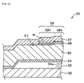
Fig. 13 is a fragmentary cross-sectional view of a piezoelectric resonator (Example 4). -
Fig. 14 is a fragmentary cross-sectional view of a piezoelectric resonator (Example 5). -
Fig. 15 is a fragmentary cross-sectional view of a piezoelectric resonator (Example 6). -
Figs. 16(a) and 16(b) are each an enlarged fragmentary view of a piezoelectric resonator (Example 7). -
Figs. 17(a-1) to 17(c-3) are each a Smith chart showing resonator characteristics (Example 7). -
Figs. 18(a) to 18(e) are each a Smith chart showing resonator characteristics (Example 8). -
Figs. 19(a) to 19(d) are each a Smith chart showing resonator characteristics (Example 9). -
Figs. 20(a) and 20(b) are each an explanatory drawing of a step of a top electrode (Example 10). -
Figs. 21(a) to 21(d) are each an explanatory drawing of a process of forming a step on the top electrode (Example 10). -
Figs. 22(a) and 22(b) are each an explanatory drawing of a step of a vibrating region (Example 11). -
Fig. 23 is a block diagram of a lattice filter (Example 12). -
Fig. 24 is a graph showing characteristics of a lattice filter (Example 12). -
Fig. 25 is a block diagram of a ladder filter (Example 13). -
Fig. 26 is a graph showing characteristics of a ladder filter (Example 13). -
Fig. 27 is a fragmentary plan view of a piezoelectric resonator (Example 14). -
- 10, 20, 30, 40, 50 piezoelectric resonator
- 12, 22, 32, 42, 52 substrate
- 13, 23, 33, 43, 53 gap
- 14, 24, 34, 44, 54 bottom electrode (conductive layer)
- 15, 25, 35, 45, 55 piezoelectric layer
- 16, 26, 36, 46, 56 top electrode (conductive layer)
- 17, 27, 37 dielectric layer
- 18, 18x, 18y, 28, 38, 48, 58 vibrating region
- 18a, 18b, 18c outer edge
- 18s, 18s', 18s", 28s, 38s, 48s, 58s central portion
- 18t, 18t, 18t', 18t", 28t, 38t, 48t, 58t peripheral portion
- 72 lattice filter
- 76 ladder filter
- Embodiments of the present invention will be described below with reference to
Figs. 5(a) to 27 . - With respect to a piezoelectric resonator including at least two conductive layers and at least one piezoelectric layer disposed between the conductive layers and a piezoelectric thin-film filter configured by a combination of the piezoelectric resonators, embodiments of the present invention have advantages (1) to (4) as follows:
- (1) A reduction in thickness of edges of a vibrating region suppresses long-wavelength spurious modes.
- (2) "A rectangle with edges each having a triangular waveform", "a rectangle with edges each having a rectangular waveform", or "a rectangle with sides that are not parallel to each other", which facilitates layout and suppresses short-wavelength-spurious modes, is used as a planar shape of the vibrating region.
- (3) The resonator formed by employing techniques described in Items (1) and (2) is used as a relatively-high-frequency resonator of resonators constituting a lattice filter, thereby suppressing ripples in the pass band width of the filter (even when a series resonator and a parallel resonator are interchanged in a lattice filter, the same characteristics are obtained).
- (4) The resonator formed by employing techniques described in Items (1) and (2) is used as a series resonator of resonators constituting a ladder filter, thereby suppressing ripples in the pass band width of the filter.
- That is, as described in Item (2), the edges having the waveform of the rectangular vibrating region scatter a wave having a wavelength comparable to the waveform at the edges to cancel a spurious wave (short-wavelength spurious wave) out. An increase in the scale of the waveform cancels a long-wavelength wave out. However, with respect to a method for canceling a long-wavelength wave, the formation of steps at the edges of the vibrating region as described in Item (1) provides more satisfactory characteristics, facilitates layout, and reduces the size of the resonator.
- However, a resonator having steps at edges of a vibrating region and having a waveform at the edges of the vibrating region was actually formed by the techniques described in Items (1) and (2). As shown in Smith charts in
Figs. 5(a) and 5(b) , it was found that characteristics at a resonant frequency or less were improved but that characteristics at the resonant frequency or more were degraded. InFigs. 5(a) and 5(b) , Symbol s represents the case where the steps are formed at the edges of the rectangular vibrating region having sides that are not parallel to each other. Symbol t represents the case where no step is formed at the edges of the rectangular vibrating region having sides that are not parallel to each other.Fig. 5(b) is an enlarged view of a portion indicated by Symbol A inFig. 5(a) . - As shown in
Fig. 6(a) , resonators 80a to 80d may be connected in the form of a lattice to form a filter. Alternatively, as shown inFig. 6(b) ,resonators -
Fig. 7 shows the relationship of characteristics of a resonator and a lattice filter formed by combining resonators (series resonator and parallel resonator) having different frequencies. A resonator having a relatively high frequency is used as the series resonator. InFig. 7 ,reference numeral 80 represents the impedance of the series resonator.Reference numeral 81 represents the impedance of the parallel resonator.Reference numeral 82 represents filter characteristics. - With respect to the filter characteristics, it is necessary to ensure a filter bandwidth while suppressing ripples in pass band width P. The characteristics in the pass band width P of the filter are affected by characteristics of the series resonator at and near the resonant frequency and the parallel resonator at and near the anti-resonant frequency. In the case where resonators according to the technique described in Item (2) are used for both of the series resonator and parallel resonator constituting the filter, the parallel resonator impairs the characteristics in the pass band width of the filter.
- Referring to
Fig. 8 , Symbol a represents filter characteristics when the technique described in Item (2) is employed for both of the series resonator and parallel resonator. Symbol b represents filter characteristics when the technique described in Item (2) is employed for only the series resonator. Symbol c represents filter characteristics when the technique described in Item (2) is not employed for any of the series resonator and parallel resonator. - In the case where the technique described in Item (2) is not employed for any of the series resonator and parallel resonator (Symbol c), a spurious wave having a frequency equal to or less than the resonant frequency of the series resonator causes the generation of ripples in the middle of the pass band width of the filter. In the case where the technique described in Item (2) is employed for both of the series resonator and parallel resonator (Symbol a), the characteristics of the parallel resonator are degraded at a frequency equal to or higher than the resonant frequency. Thus, as shown in Arrow X, the characteristics around the left shoulder in the pass band width of the filter are degraded; hence, the filter bandwidth is not ensured. In the case where the technique described in Item (2) is employed for only the series resonator (Symbol b), it is possible to suppress the ripples in the middle of the pass band width of the filter while ensuring the filter band width.
- A first to fourteenth embodiments will be described below with reference to
Figs. 9(a) to 27 . - As shown in
Figs. 9(a) and 9(b) , thepiezoelectric resonator 10 includes abottom electrode 14, apiezoelectric layer 15, atop electrode 16, and adielectric film 17 stacked in that order on asubstrate 12. Thebottom electrode 14 has a portion supported by thesubstrate 12 and a floating portion remote from thesubstrate 12 with agap 13. A vibratingregion 18 in which thepiezoelectric layer 15 is disposed between thebottom electrode 14 and thetop electrode 16 is arranged on the floating portion. The vibratingregion 18 is a portion in which thebottom electrode 14 and thetop electrode 16 overlap one another when viewed in the thickness direction (the direction perpendicular to the paper plane inFig. 9(b) ). The vibratingregion 18 is acoustically isolated from thesubstrate 12 via thegap 13. Instead of thegap 13, a sound reflecting layer may be disposed between thesubstrate 12 and the vibratingregion 18 to acoustically isolate the vibratingregion 18 from thesubstrate 12. - The vibrating
region 18 includes aperipheral portion 18t extending alongouter edges 18a of the vibratingregion 18; and acentral portion 18s extending inside theperipheral portion 18t, when viewed in the thickness direction. InFig. 9(b) , theboundary 18k between theperipheral portion 18t and thecentral portion 18s of the vibratingregion 18 is represented by a broken line. - As shown in
Fig. 9(b) , the shape of theouter edges 18a of the vibratingregion 18 is a substantial rectangle when viewed in the thickness direction. Sides of the substantial rectangle each have a waveform. That is, anend 14a of thebottom electrode 14, anend 16a of thetop electrode 16,portions outer edges 18a of the vibratingregion 18, each have a waveform in which a triangular wave segment is repeated. - Outer edges 18a of the vibrating
region 18 may have a waveform. For example, a rectangular waveform may be used as inouter edges 18b of a vibratingregion 18x shown inFig. 10 that is a fragmentary plan view. Alternatively, a sinusoidal waveform may be used. The waveform of theouter edges 18a may have an irregular period and irregular amplitude. InFig. 10 , theboundary 18k' between aperipheral portion 18t' and acentral portion 18s' of the vibratingregion 18x is represented by a broken line. - As shown in
Fig. 9(a) , thebottom electrode 14, thepiezoelectric layer 15, and thetop electrode 16 each have a substantially constant thickness. In thedielectric film 17, a portion constituting thecentral portion 18s of the vibratingregion 18 has a thickness larger than that of the remainder. Thus, in the vibratingregion 18, theperipheral portion 18t has a thickness smaller than that of thecentral portion 18s, thereby forming a step in the vibratingregion 18. A portion not including the step may be present. - The vibrating
region 18 has the type II dispersion property shown inFig. 4 . - Specifically, for example, the
dielectric film 17 composed of SiO2 is formed on thepiezoelectric layer 15 composed of AlN. The width W of thedielectric film 17 at theperipheral portion 18t of the vibratingregion 18 is set at about 10 µm. A change in thickness Δt due to the step is set at about 20 nm. - As shown in
Fig. 9(b) , the shape of theouter edges 18a of the vibratingregion 18 is the substantial rectangle, and each of the sides of the substantial rectangle has the triangular waveform; hence, thepiezoelectric resonator 10 can suppress short-wavelength spurious modes. This is probably because among waves reflected from theouter edges 18a of the vibratingregion 18, wave components having wavelengths corresponding to the shape of theouter edges 18a cancel each other out, thereby eliminating the generation of an undesired component due to interference. - Alternatively, by changing the thickness of the
dielectric film 17 in such a manner that theperipheral portion 18t of the vibratingregion 18 has a thickness smaller than that of thecentral portion 18s, long-wavelength spurious modes can be suppressed. - As shown in
Fig. 11 , the shape ofouter edges 18c of a vibratingregion 18y is a substantial rectangle, and sides of the substantial rectangle each have an irregular waveform. InFig. 11 , theboundary 18k " between aperipheral portion 18t" and acentral portion 18s" of the vibratingregion 18y is represented by a broken line. - Also in the second embodiment, short-wavelength spurious modes can be suppressed. This is probably because waves reflected from the
outer edges 18c cancel each other out by scattering, thereby eliminating the generation of an undesired component due to interference. - In the piezoelectric resonator according to the second embodiment, the
peripheral portion 18t" of the vibratingregion 18y has a thickness smaller than that of thecentral portion 18s'', as in the first embodiment, thereby suppressing long-wavelength spurious modes. - In the
piezoelectric resonator 20, a vibratingregion 28 is acoustically isolated from asubstrate 22 with agap 23, as in the first embodiment. Unlike the first embodiment, in atop electrode 26, a portion constituting acentral portion 28s of the vibratingregion 28 has a thickness larger than that of the remainder. Abottom electrode 24, apiezoelectric layer 25, and adielectric layer 27 each have a substantially constant thickness. Thus, aperipheral portion 28t of the vibrating region has a thickness smaller than that of thecentral portion 28s, thereby forming a step in the vibratingregion 28. - Specifically, for example, the
dielectric layer 27 composed of SiO2 is formed on thepiezoelectric layer 25 composed of AlN. The width W of aportion 26a of thetop electrode 26, which is theperipheral portion 28t of the vibratingregion 28 is set at about 10 µm. A change in thickness Δt is set at about 5 nm. The planar shape of the vibratingregion 28 is a rectangle. Outer edges of the vibratingregion 28 each have a waveform. A drawing is the same asFig. 9(b) in the first embodiment and is thus omitted. - The
piezoelectric resonator 20 can suppress both long-wavelength spurious modes and short-wavelength spurious modes as in the first embodiment. - In a
piezoelectric resonator 30, a vibratingregion 38 is acoustically isolated from asubstrate 32 with agap 33, as in the first embodiment. Unlike the first embodiment, in apiezoelectric layer 35, aportion 34a constituting acentral portion 38s of the vibratingregion 38 has a thickness larger than that of the remainder. Abottom electrode 34, atop electrode 36, and adielectric layer 37 each have a substantially constant thickness. Thus, aperipheral portion 38t of the vibratingregion 38 has a thickness smaller than that of thecentral portion 38s, thereby forming a step in the vibratingregion 38. - Specifically, for example, the
dielectric layer 37 composed of SiO2 is formed on thepiezoelectric layer 35 composed of AlN. The width W of the step on thepiezoelectric layer 35 is set at about 10 µm. A change in thickness Δt is set at about 20 nm. The planar shape of the vibratingregion 38 is a rectangle. Outer edges of the vibratingregion 38 each have a waveform. A drawing is the same asFig. 9(b) in the first embodiment and is thus omitted. - The
piezoelectric resonator 30 can suppress both long-wavelength spurious modes and short-wavelength spurious modes as in the first embodiment. - Unlike the first embodiment, the
piezoelectric resonator 40 does not include a dielectric layer. That is, a vibratingregion 48 acoustically isolated from asubstrate 42 with agap 43 includes abottom electrode 44, apiezoelectric layer 45, and atop electrode 46. - In the
top electrode 46, a portion constituting acentral portion 48s of the vibratingregion 48 has a thickness larger than that of the remainder. Thebottom electrode 44 and thepiezoelectric layer 45 each have a substantially constant thickness. Thus, aperipheral portion 48t of the vibratingregion 48 has a thickness smaller than that of thecentral portion 48s, thereby forming a step in the vibratingregion 48. - Specifically, for example, the step is formed on the
top electrode 46 disposed on thepiezoelectric layer 45 composed of AlN. The width W of the step is set at about 10 µm. A change in thickness Δt is set at about 5 nm. The planar shape of the vibratingregion 48 is a rectangle. Outer edges of the vibratingregion 48 each have a waveform. A drawing is the same asFig. 9(b) in the first embodiment and is thus omitted. - The
piezoelectric resonator 40 can suppress both long-wavelength spurious modes and short-wavelength spurious modes as in the first embodiment. - Unlike the first embodiment, the
piezoelectric resonator 50 does not include a dielectric layer. That is, a vibratingregion 58 acoustically isolated from asubstrate 52 with agap 53 includes abottom electrode 54, apiezoelectric layer 55, and atop electrode 56. - In the
piezoelectric layer 55, a portion constituting acentral portion 58s of the vibratingregion 58 has larger than that of the remainder. Thebottom electrode 54 and thetop electrode 56 each have a substantially constant thickness. Thus, aperipheral portion 58t of the vibratingregion 58 has a thickness smaller than that of thecentral portion 58s, thereby forming a step in the vibratingregion 58. - Specifically, for example, the step is formed on the
piezoelectric layer 45 composed of AlN. The width W of the step is set at about 10 µm. A change in thickness Δt is set at about 20 nm. The planar shape of the vibratingregion 58 is a rectangle. Outer edges of the vibratingregion 58 each have a waveform. A drawing is the same asFig. 9(b) in the first embodiment and is thus omitted. - The
piezoelectric resonator 50 can suppress both long-wavelength spurious modes and short-wavelength spurious modes as in the first embodiment. - In the piezoelectric resonator, a vibrating region is acoustically isolated from a substrate with a gap, as in the first embodiment. Unlike the first embodiment, a bottom electrode, a piezoelectric layer, a top electrode, and a dielectric layer that constitute the vibrating region each have a substantially constant thickness.
- The planar shape of outer edges of the vibrating region is a substantial rectangle as in the first embodiment.
Sides of the substantially rectangular planar shape of the outer edges of the vibrating region each have a triangular waveform shown inFig. 16(a) or a rectangular waveform shown inFig. 16(b) . As shown inFig. 16(a) and 16(b) , let the length and total amplitude of the triangular or rectangular wave per period (wavelength) be λ1 and λ2, respectively. Characteristics of the resonator are changed depending on λ1 and λ2. - In the piezoelectric resonator according to the seventh embodiment, the outer edges of the vibrating region each have the waveform. They scatter waves comparable to the waveform of the outer edges of the vibrating region to eliminate spurious waves. The length of the waveform of the outer edges of the vibrating region may be 1/4 or more times a wavelength to be suppressed. Each of λ1 and λ2 may be 0.5 or more times the thickness of the piezoelectric layer. Experiments demonstrated that each of λ1 and λ2 has an upper limit.
-
Figs. 17(a-1) to 17(c-3) are each a Smith chart showing characteristics (experimental values) of the piezoelectric resonator for use in 1.8-GHz band, the piezoelectric resonator including the piezoelectric layer having a thickness of 1.6 µm and not having a step in the vibrating region, when λ1 and λ2 of the triangular or rectangular wave of each side of the substantial rectangular planar shape of the outer edges of the vibrating region are changed in the ranges of λ1 = 10 to 30 (µm) and λ2 = 5 to 15 (µm). With respect to λ1, inFigs. 17(a-1) and 17(b-1) , λ1 = 10 (µm). InFigs. 17(a-2) and (b-2) , λ1 = (20 µm). InFig. 17(a-3), 17(b-3), and 17(c-3) , λ1 = 30 (µm). With respect to λ2, inFigs. 17(a-1), 17(a-2), and 17(a-3) , λ2 = 5 (µm). InFigs. 17(b-1), 17(b-2), and 17(b-3) , λ2 = 10 (µm). InFig. 17(c-3) ,λ 2 = 15 (µm). -
Figs. 17(a-1) to 17(c-3) show that when λ1 ≤ 20 µm and λ2 ≤ 10 µm, short-wavelength spurious modes are suppressed. The upper limit of λ1 is 12.5 times the piezoelectric layer (20/1.6 = 12.5). The upper limit of λ2 is 6.25 times the piezoelectric layer (10/1.6). -
Figs. 18(a) to 18(e) are each a Smith chart showing characteristics of the piezoelectric resonator for use in 1.8-GHz band, the piezoelectric resonator including the dielectric layer having a thickness of 1.6 µm, when the width W of the step is changed in the range of W = 0 to 20 (µm) while a change in the thickness Δt of the step formed on the dielectric layer composed of SiO2 is a constant (20 nm). InFig. 18(a) , W = 0 (µm), i.e., a step is absent on the vibrating region. InFig. 18(b) , W = 5 (µm). InFig. 18(c) , W = 10 (µm). InFig. 18(d) , W = 15 (µm). InFig. 18(e) , W = 20 (µm) . -
Figs. 18(a) to 18(e) show that when the step width W is in the range of 5 ≤ W < 15, long-wavelength spurious modes are suppressed. The results demonstrate that the lower limit of the step width W is about three times the thickness of the piezoelectric layer. The upper limit of the step width W is about is about nine times the thickness of the piezoelectric layer. -
Figs. 19(a) to 19(d) are each a Smith chart showing characteristics of the piezoelectric resonator for use in 1.8-GHz band, the piezoelectric resonator including the dielectric layer having a thickness of 1.6 µm, when a change in the thickness Δt of the step is changed in the range of Δt = 0 to 40 (nm) while the width W of the step formed on the dielectric layer composed of SiO2 is a constant (10 µm). InFig. 19(a) , Δt = 0 (i.e., a step is absent). InFig. 19(b) , Δt = 20 (nm). InFig. 19(c) , Δt = 30 (nm). InFig. 19(d) , Δt = 40 (nm). -
Figs. 19(a) to 19(d) show that when the change in the thickness Δt of the step is in the range of 0 < Δt < 30, long-wavelength spurious modes are suppressed. - As shown in
Figs. 12 and14 , in the case where steps are formed on the vibratingregions top electrodes - As shown in
Figs. 20(a) and 20(b) , atop electrode 60 includes at least onelayer 64 having a low etching resistance, the at least onelayer 64 being composed of A1, Au, or the like and located as the uppermost layer; and at least onelayer 62 having a high etching resistance, the at least onelayer 62 being composed of Pt or the like and located below the at least onelayer 64. - When the formation of the step is stopped in the middle of the
uppermost layer 64 as shown inFig. 20(b) , controllability is poor. When thelayer 64 having a low etching resistance is completely removed by etching, etching is stopped at thelayer 62 having a high etching resistance; hence, controllability is satisfactory. - The
top electrode 60 having a step may be formed by a procedure shown inFigs. 21(a) to 21(d) . - As shown in
Fig. 21(a) , thelayer 64 having a low etching resistance and composed of Al, Au, or the like is formed on thelayer 62 having a high etching resistance and composed of Pt or the like. As shown inFig. 21(b) , an etching mask is formed with a resist 65. As shown inFig. 21(c) , for a portion to be formed into a step, thelayer 64 having a low etching resistance is completely removed by etching with the mask. As shown inFig. 21(d) , the resist 65 is removed. - Examples of a material usable for the
layer 62 having a relatively high etching resistance include metals, such as W, Mo, Ir, Os, Re, and Ru, as well as Pt. Examples of a material usable for thelayer 64 having a relatively low etching resistance include metals, such as Ti, NiCr, Cr, and Cu, as well as Al and Au. Two or more metals may be used for each of thelayers - The use of the top electrode including the two layers having different etching resistances facilitates formation of the step on the vibrating region.
- As shown in
Fig. 22(a) , aninclined surface 66k is formed in the vicinity of theboundary 66b between acentral portion 66s and aperipheral portion 66t of a vibratingregion 66 to form a tapered profile with a gradual change in the thickness of the vibratingregion 66. Thereby, a step is formed on the vibratingregion 66. - Alternatively, as shown in
Fig. 22(b) that is a fragmentary cross-sectional view, a substantiallyvertical surface 68k is formed in the vicinity of theboundary 68b between acentral portion 68s and aperipheral portion 68t of a vibratingregion 68 to form a step profile having a sharp change in the thickness of the vibratingregion 68. Thereby, a step is formed on the vibratingregion 68. - It is difficult to obtain the substantially right-angled profile as shown in
Fig. 22(b) by etching or a lift-off method. Such a tapered profile as shown inFig. 22(a) is easily obtained to a varying degree. Calculation and actual measurement demonstrated that the tapered step shown inFig. 22(a) also has a spurious-mode-suppressing effect comparable to the step shown inFig. 22(b) . - As show in
Fig. 23 , alattice filter 72 is configured by connectingseries resonators 70a to 70d andparallel resonators 71a to 71d in the form of a lattice.Fig. 23 shows the case where the number of poles is two. The number of poles may be one or three or more. - In the
lattice filter 72, only each of theseries resonators 70a to 70d each having a relatively high frequency has a structure capable of suppressing long-wavelength spurious modes. That is, only each of theseries resonators 70a to 70d each having a relatively high frequency has a step along outer edges of a vibrating region. -
Fig. 24 shows exemplary characteristics of thelattice filter 72.Reference numeral 70s represents impedance characteristics when theseries resonators 70a to 70d have the same characteristic. Reference numeral 71s represents impedance characteristics when theparallel resonators 71a to 71d have the same characteristic.Reference numeral 72s represents filter characteristics of thelattice filter 72 including theseries resonators 70a to 70d having the impedance characteristics represented by reference numeral 70s and theparallel resonators 71a to 71d having the impedance characteristics represented by reference numeral 71s. - The
lattice filter 72 has satisfactory spurious characteristics with ripples suppressed in the pass band width of the filter. - As shown in
Fig. 25 , theladder filter 76 is configured by connectingseries resonators parallel resonators Fig. 25 shows the case where the number of poles is two. The number of poles may be one or three or more. - In the
ladder filter 76, only each of theseries resonators 74a to 74b has a structure capable of suppressing long-wavelength spurious modes. That is, only each of theseries resonators 74a to 74b has a step along outer edges of a vibrating region, wherein a peripheral portion of the vibrating region has a thickness smaller than that of a central portion of the vibrating region. -
Fig. 26 shows exemplary characteristics of theladder filter 76.Reference numeral 74s represents impedance characteristics when theseries resonators parallel resonators Reference numeral 76s represents filter characteristics of theladder filter 76 including theseries resonators parallel resonators - The
ladder filter 76 has satisfactory spurious characteristics with ripples suppressed in the pass band width of the filter. - As shown in
Fig. 27 , the planar shape of a vibratingregion 78 of the piezoelectric resonator according to the fourteenth embodiment is a rectangle with sides that are not parallel to each other. Each ofsides 78a to 78d of the rectangular planar shape of the vibratingregion 78 does not have a waveform but is straight. Theperipheral portion 78t of the vibratingregion 78 has a thickness smaller than that of a central portion 78s of the vibratingregion 78. Theboundary 78k between the central portion 78s and theperipheral portion 78t of the vibratingregion 78 is represented by a broken line. - The piezoelectric resonator according to the fourteenth embodiment reduces long-wavelength spurious modes. For example, a step is formed on the vibrating
region 78 by changing a dielectric layer composed of SiO2. The characteristics of the piezoelectric resonator in which the width of the step on the vibratingregion 78 is 10 µm and in which a change in the thickness of the step is 20 nm are the same as that represented by Symbol s inFigs. 5(a) and 5(b) . <Conclusion> As described above, according to preferred embodiments of the present invention, there is provided a resonator having a shape that facilitates layout and having suppressed long-wavelength spurious modes and short-wavelength spurious modes. Furthermore, there is provided a filter having satisfactory ripple-suppressed filter characteristics while the pass band width of the filter is ensured. - The present invention is not limited to the above-described equivalents. Various modifications may be made.
- For example, instead of the gap, the vibrating region may be acoustically isolated from the substrate by a sound reflecting layer disposed between the substrate and the vibrating region or an opening formed in the substrate. The piezoelectric layer may be composed of ZnO having type II dispersion characteristics. The dielectric layer may be composed of AlN, SiN, or the like in place of SiO2. The step on the vibrating region may be formed by changing the thicknesses of two or more of the conductive layer, the piezoelectric layer, and the dielectric layer. The piezoelectric resonator may have a structure without the dielectric layer.
Claims (22)
- A piezoelectric resonator comprising:a substrate;a pair of conductive layers disposed on the substrate; anda piezoelectric layer disposed between the pair of conductive layers,wherein at least a region of the piezoelectric layer disposed between the pair of conductive layers (hereinafter, the region being referred to as a "vibrating region") is acoustically isolated from the substrate,
in a dispersion curve in which the vertical axis represents the frequency, the horizontal axis on the right side of the vertical axis represents the real wave number, and the horizontal axis on the left side of the vertical axis represents the imaginary wave number, when the frequency is lower than a cut-off angular frequency ωc, the vibrating region has a real wave number,
the shape of the vibrating region when viewed in the thickness direction of the pair of conductive layers and the piezoelectric layer (hereinafter, the shape being referred to as a "planar shape") is a substantial polygon, sides of the substantial polygon are not parallel to each other, and
the vibrating region includes a peripheral portion extending along outer edges of the planar shape and having a relatively small thickness; and a central portion extending inside the peripheral portion and having a relatively large thickness. - A piezoelectric resonator comprising:a substrate;a pair of conductive layers; anda piezoelectric layer disposed between the pair of conductive layers,wherein at least a region of the piezoelectric layer disposed between the pair of conductive layers (hereinafter, the region being referred to as a "vibrating region") is acoustically isolated from the substrate,
wherein in a dispersion curve in which the vertical axis represents the frequency, the horizontal axis on the right side of the vertical axis represents the real wave number, and the horizontal axis on the left side of the vertical axis represents the imaginary wave number, when the frequency is lower than a cut-off angular frequency ωc, the vibrating region has a real wave number,
the shape of the vibrating region when viewed in the thickness direction of the pair of conductive layers and the piezoelectric layer (hereinafter, the shape being referred to as a "planar shape") is a substantial rectangle, sides of the substantial rectangle each have a waveform in which a curved or angular wave segment is repeated, and
the vibrating region includes a peripheral portion extending along outer edges of the planar shape and having a relatively small thickness; and a central portion extending inside the peripheral portion and having a relatively large thickness. - The piezoelectric resonator according to claim 1, further comprising a dielectric layer extending along at least one conductive layer of the pair of conductive layers, the dielectric layer being disposed on a side of the at least one conductive layer opposite the side adjacent to the piezoelectric layer,
wherein the dielectric layer is arranged so as to be superposed at least on the vibrating region when viewed in the thickness direction of the pair of conductive layers and the piezoelectric layer. - The piezoelectric resonator according to claim 2, further comprising a dielectric layer extending along at least one conductive layer of the pair of conductive layers, the dielectric layer being disposed on a side of the at least one conductive layer opposite the side adjacent to the piezoelectric layer,
wherein the dielectric layer is arranged so as to be superposed at least on the vibrating region when viewed in the thickness direction of the pair of conductive layers and the piezoelectric layer. - The piezoelectric resonator according to any one of claims 1 to 4,
wherein the planar shape of the vibrating region suppresses a spurious Lamb wave having a relatively short wavelength that is equal to or less than twice the thickness of the piezoelectric layer, and
the thicknesses of the peripheral portion and the central portion suppress a spurious Lamb wave having a relatively long wavelength that is five or more times the thickness of the piezoelectric layer. - The piezoelectric resonator according to claim 1, 3, or 5, wherein each of the outer edges of the vibrating region with a substantially rectangular planar shape has at least one waveform selected from a triangular wave, a rectangular wave, a sinusoidal wave, and an irregular wave or has a waveform obtained by combining two or more waves selected from a triangular wave, a rectangular wave, a sinusoidal wave, and an irregular wave.
- The piezoelectric resonator according to claim 1, 3, 5, or 6, wherein the vibrating region has a substantially rectangular planar shape, and
each of the outer edges of the planar shape has a waveform in which a single wave segment having a length of 0.5 to 12.5 times the thickness of the piezoelectric layer is repeated. - The piezoelectric resonator according to claim 1, 3, 5, or 6, wherein the vibrating region has a substantially rectangular planar shape, and
each of the outer edges of the planar shape has a waveform in which a single wave segment having a total amplitude of 0.5 to 6.25 times the thickness of the piezoelectric layer is repeated. - The piezoelectric resonator according to any one of claims 1 to 8, wherein at least one of the pair of conductive layers has a relatively small thickness at a portion included in the peripheral portion of the vibrating region and has a relatively large thickness at a portion included in the central portion of the vibrating region.
- The piezoelectric resonator according to any one of claims 1 to 8, wherein the piezoelectric layer has a relatively small thickness at a portion included in the peripheral portion of the vibrating region and has a relatively large thickness at a portion included in the central portion of the vibrating region.
- The piezoelectric resonator according to any one of claims 3 to 8, wherein the dielectric layer has a relatively small thickness at a portion included in the peripheral portion of the vibrating region and has a relatively large thickness at a portion included in the central portion of the vibrating region.
- The piezoelectric resonator according to any one of claims 1 to 11, wherein the peripheral portion of the vibrating region has a tapered profile with a gradual change in thickness in the vicinity of the boundary between the peripheral portion and the central portion of the vibrating region.
- The piezoelectric resonator according to any one of claims 1 to 11, wherein the vibrating region has a step profile having a sharp change in thickness at the boundary between the peripheral portion and the central portion of the vibrating region.
- The piezoelectric resonator according to any one of claims 1 to 8, wherein the width of the peripheral portion of the vibrating region is 3 to 9 times the thickness of the piezoelectric layer.
- The piezoelectric resonator according to any one of claims 1 to 9, wherein at least one conductive layer of the pair of conductive layers includes at least two sublayers stacked, one sublayer of the at least two sublayers is located adjacent to the piezoelectric layer, and the other sublayer of the at least two sublayers is located remote from the piezoelectric layer and is arranged inside and apart from an end of the one sublayer in the vibrating region.
- The piezoelectric resonator according to any one of claims 1 to 9, wherein at least one of the pair of conductive layers includes at least two sublayers stacked, the at least two sublayers having different etching resistances,
one sublayer of the at least two sublayers, the one sublayer being located adjacent to the piezoelectric layer, has a relatively high etching resistance,
the other sublayer of the at least two sublayers, the other sublayer being located remote from the piezoelectric layer, has a relatively low etching resistance, and
the other sublayer is arranged inside and apart from an end of the one sublayer by etching an end portion of the other sublayer until the one sublayer is exposed. - The piezoelectric resonator according to claim 16, wherein the one sublayer having a relatively high etching resistance contains at least one metal selected from the group consisting of Pt, W, Mo, Ir, Os, Re, and Ru, and
the other sublayer having a relatively low etching resistance contains at least one metal selected from the group consisting of Al, Ti, Au, NiCr, Cr, and Cu. - The piezoelectric resonator according to any one of claims 1 to 17, wherein the piezoelectric material constituting the piezoelectric layer is AlN or ZnO.
- The piezoelectric resonator according to any one of claims 1 to 18, wherein the dielectric layer is composed of at least one dielectric material selected from the group consisting of SiO2, A1N, and SiN.
- A piezoelectric thin-film filter comprising:a plurality of piezoelectric resonators, wherein only some of the plurality of piezoelectric resonators are the piezoelectric resonators according to any of claims 1 to 19.
- A piezoelectric thin-film filter comprising:a plurality of piezoelectric resonators connected in the form of a ladder, wherein one or more of the piezoelectric resonators are connected in series, and at least one of the series-connected piezoelectric resonators is the piezoelectric resonator according to any one of claims 1 to 19.
- A piezoelectric thin-film filter comprising:a plurality of piezoelectric resonators connected in the form of a ladder, wherein at least one relatively-high-frequency piezoelectric resonator of the plurality of piezoelectric resonators is the piezoelectric resonator according to any one of claims 1 to 19.
Applications Claiming Priority (2)
| Application Number | Priority Date | Filing Date | Title |
|---|---|---|---|
| JP2005163064 | 2005-06-02 | ||
| PCT/JP2006/310308 WO2006129532A1 (en) | 2005-06-02 | 2006-05-24 | Piezoelectric resonator and piezoelectric thin film filter |
Publications (2)
| Publication Number | Publication Date |
|---|---|
| EP1887688A1 true EP1887688A1 (en) | 2008-02-13 |
| EP1887688A4 EP1887688A4 (en) | 2009-08-05 |
Family
ID=37481461
Family Applications (1)
| Application Number | Title | Priority Date | Filing Date |
|---|---|---|---|
| EP06756514A Withdrawn EP1887688A4 (en) | 2005-06-02 | 2006-05-24 | Piezoelectric resonator and piezoelectric thin film filter |
Country Status (4)
| Country | Link |
|---|---|
| US (1) | US7636027B2 (en) |
| EP (1) | EP1887688A4 (en) |
| JP (1) | JP4508241B2 (en) |
| WO (1) | WO2006129532A1 (en) |
Cited By (3)
| Publication number | Priority date | Publication date | Assignee | Title |
|---|---|---|---|---|
| DE102015118437A1 (en) * | 2015-10-28 | 2017-05-04 | Snaptrack, Inc. | Layer arrangement for a volume wave component |
| DE102018208454A1 (en) * | 2018-02-21 | 2019-08-22 | Globalfoundries Singapore Pte. Ltd. | Acoustic resonator and zigzagged electrode filter and method of making the same |
| US12395149B2 (en) | 2019-12-06 | 2025-08-19 | Murata Manufacturing Co., Ltd. | Acoustic wave device |
Families Citing this family (24)
| Publication number | Priority date | Publication date | Assignee | Title |
|---|---|---|---|---|
| KR20090109541A (en) * | 2007-01-17 | 2009-10-20 | 우베 고산 가부시키가이샤 | Thin Film Piezoelectric Resonators and Thin Film Piezoelectric Filters |
| JP5013227B2 (en) * | 2007-04-11 | 2012-08-29 | 株式会社村田製作所 | Piezoelectric thin film filter |
| JP4935788B2 (en) * | 2008-09-30 | 2012-05-23 | セイコーエプソン株式会社 | Piezoelectric thin film resonator and manufacturing method thereof |
| JP5202252B2 (en) * | 2008-11-27 | 2013-06-05 | 京セラ株式会社 | Acoustic wave resonator |
| US9991871B2 (en) * | 2011-02-28 | 2018-06-05 | Avago Technologies General Ip (Singapore) Pte. Ltd. | Bulk acoustic wave resonator comprising a ring |
| JP5994850B2 (en) * | 2012-05-22 | 2016-09-21 | 株式会社村田製作所 | Bulk wave resonator |
| US10367472B2 (en) * | 2012-10-25 | 2019-07-30 | Avago Technologies International Sales Pte. Limited | Acoustic resonator having integrated lateral feature and temperature compensation feature |
| KR101959204B1 (en) * | 2013-01-09 | 2019-07-04 | 삼성전자주식회사 | Radio frequency filter and manufacturing mathod thereof |
| CN103929148B (en) * | 2013-01-11 | 2017-09-19 | 中兴通讯股份有限公司 | A kind of filter with low insertion loss piezoelectric sound wave bandpass filter and implementation method |
| JP6441761B2 (en) | 2015-07-29 | 2018-12-19 | 太陽誘電株式会社 | Piezoelectric thin film resonator and filter |
| JP6469601B2 (en) * | 2016-02-05 | 2019-02-13 | 太陽誘電株式会社 | Piezoelectric thin film resonator, filter and duplexer |
| TWI578698B (en) * | 2016-04-11 | 2017-04-11 | 穩懋半導體股份有限公司 | A resonance structure of bulk acoustic wave resonator |
| JP6855227B2 (en) * | 2016-12-12 | 2021-04-07 | 日本電波工業株式会社 | Piezoelectric vibrating pieces and piezoelectric devices |
| DE102017118804B3 (en) * | 2017-08-17 | 2018-11-15 | RF360 Europe GmbH | Acoustic resonator with high Q |
| KR20200030478A (en) | 2018-09-12 | 2020-03-20 | 스카이워크스 글로벌 피티이. 엘티디. | Recess frame structure for a bulk acoustic wave resonator |
| US11964483B2 (en) | 2019-04-24 | 2024-04-23 | Rohm Co., Ltd. | Piezoelectric film utilization device |
| SG10202004451PA (en) * | 2019-05-23 | 2020-12-30 | Skyworks Global Pte Ltd | Film bulk acoustic resonator including recessed frame with scattering sides |
| CN111010116B (en) * | 2019-08-13 | 2023-12-15 | 天津大学 | Bulk acoustic wave resonators, filters and electronic devices with highly graded raised structures |
| CN210405247U (en) | 2019-11-12 | 2020-04-24 | 迈感微电子(上海)有限公司 | Bulk acoustic wave resonator |
| CN111554799A (en) * | 2020-04-23 | 2020-08-18 | 瑞声声学科技(深圳)有限公司 | Planarization method |
| US12483225B2 (en) | 2021-05-14 | 2025-11-25 | Skyworks Global Pte. Ltd. | Bulk acoustic wave resonator with oxide raised frame |
| KR20220163883A (en) | 2021-06-03 | 2022-12-12 | 스카이워크스 글로벌 피티이. 엘티디. | Radio frequency acoustic device with laterally distributed reflectors |
| JP7627995B2 (en) * | 2021-06-11 | 2025-02-07 | 太陽誘電株式会社 | Piezoelectric thin film resonator, filter, and multiplexer |
| US12334908B2 (en) | 2021-12-10 | 2025-06-17 | Skyworks Solutions, Inc. | Bulk acoustic wave filters for improving noise factor |
Family Cites Families (25)
| Publication number | Priority date | Publication date | Assignee | Title |
|---|---|---|---|---|
| WO1998056049A1 (en) | 1997-06-05 | 1998-12-10 | Motorola Inc. | Electrode edge wave patterns for piezoelectric resonator |
| US5903087A (en) * | 1997-06-05 | 1999-05-11 | Motorola Inc. | Electrode edge wave patterns for piezoelectric resonator |
| US6150703A (en) * | 1998-06-29 | 2000-11-21 | Trw Inc. | Lateral mode suppression in semiconductor bulk acoustic resonator (SBAR) devices using tapered electrodes, and electrodes edge damping materials |
| US6215375B1 (en) * | 1999-03-30 | 2001-04-10 | Agilent Technologies, Inc. | Bulk acoustic wave resonator with improved lateral mode suppression |
| FI107660B (en) * | 1999-07-19 | 2001-09-14 | Nokia Mobile Phones Ltd | resonator |
| US6339276B1 (en) * | 1999-11-01 | 2002-01-15 | Agere Systems Guardian Corp. | Incremental tuning process for electrical resonators based on mechanical motion |
| US6307447B1 (en) * | 1999-11-01 | 2001-10-23 | Agere Systems Guardian Corp. | Tuning mechanical resonators for electrical filter |
| JP2001211052A (en) * | 2000-01-26 | 2001-08-03 | Murata Mfg Co Ltd | Piezoelectric resonator |
| US6420202B1 (en) * | 2000-05-16 | 2002-07-16 | Agere Systems Guardian Corp. | Method for shaping thin film resonators to shape acoustic modes therein |
| JP2002374144A (en) * | 2001-06-15 | 2002-12-26 | Ube Electronics Ltd | Thin film piezoelectric resonator |
| KR100398365B1 (en) * | 2001-06-25 | 2003-09-19 | 삼성전기주식회사 | Film Bulk Acoustic Resonator with Improved Lateral Mode Suppression |
| JP2003158442A (en) * | 2001-11-21 | 2003-05-30 | Tdk Corp | Piezoelectric thin film resonator element and filter using the same |
| JP3969224B2 (en) * | 2002-01-08 | 2007-09-05 | 株式会社村田製作所 | Piezoelectric resonator and piezoelectric filter / duplexer / communication device using the same |
| DE10241425B4 (en) | 2002-09-06 | 2015-06-18 | Epcos Ag | Oscillator operating with acoustic waves with suppression of interfering secondary modes |
| US6943648B2 (en) * | 2003-05-01 | 2005-09-13 | Intel Corporation | Methods for forming a frequency bulk acoustic resonator with uniform frequency utilizing multiple trimming layers and structures formed thereby |
| US6975184B2 (en) * | 2003-05-30 | 2005-12-13 | Intel Corporation | Adjusting the frequency of film bulk acoustic resonators |
| US6954121B2 (en) * | 2003-06-09 | 2005-10-11 | Agilent Technologies, Inc. | Method for controlling piezoelectric coupling coefficient in film bulk acoustic resonators and apparatus embodying the method |
| US7230367B2 (en) * | 2003-11-07 | 2007-06-12 | Matsushita Electric Industrial Co., Ltd. | Piezoelectric resonator, production method thereof, filter, duplexer, and communication device |
| JP2005159402A (en) * | 2003-11-20 | 2005-06-16 | Matsushita Electric Ind Co Ltd | Acoustic resonator |
| JP2005197983A (en) * | 2004-01-07 | 2005-07-21 | Tdk Corp | Thin film bulk wave resonator |
| US7161448B2 (en) * | 2004-06-14 | 2007-01-09 | Avago Technologies Wireless Ip (Singapore) Pte. Ltd. | Acoustic resonator performance enhancements using recessed region |
| US7280007B2 (en) * | 2004-11-15 | 2007-10-09 | Avago Technologies General Ip (Singapore) Pte. Ltd. | Thin film bulk acoustic resonator with a mass loaded perimeter |
| US7388454B2 (en) * | 2004-10-01 | 2008-06-17 | Avago Technologies Wireless Ip Pte Ltd | Acoustic resonator performance enhancement using alternating frame structure |
| US7791434B2 (en) * | 2004-12-22 | 2010-09-07 | Avago Technologies Wireless Ip (Singapore) Pte. Ltd. | Acoustic resonator performance enhancement using selective metal etch and having a trench in the piezoelectric |
| JP2006319796A (en) * | 2005-05-13 | 2006-11-24 | Toshiba Corp | Thin film bulk acoustic resonator |
-
2006
- 2006-05-24 EP EP06756514A patent/EP1887688A4/en not_active Withdrawn
- 2006-05-24 JP JP2007518929A patent/JP4508241B2/en active Active
- 2006-05-24 WO PCT/JP2006/310308 patent/WO2006129532A1/en not_active Ceased
-
2007
- 2007-10-12 US US11/871,285 patent/US7636027B2/en active Active
Cited By (7)
| Publication number | Priority date | Publication date | Assignee | Title |
|---|---|---|---|---|
| DE102015118437A1 (en) * | 2015-10-28 | 2017-05-04 | Snaptrack, Inc. | Layer arrangement for a volume wave component |
| DE102015118437B4 (en) * | 2015-10-28 | 2017-11-16 | Snaptrack, Inc. | Layer arrangement for a volume wave component |
| DE102018208454A1 (en) * | 2018-02-21 | 2019-08-22 | Globalfoundries Singapore Pte. Ltd. | Acoustic resonator and zigzagged electrode filter and method of making the same |
| DE102018208454B4 (en) | 2018-02-21 | 2020-04-23 | Globalfoundries Singapore Pte. Ltd. | Acoustic resonator and filter with an electrode having a zigzag edge and method for producing the same |
| US11233496B2 (en) | 2018-02-21 | 2022-01-25 | Vanguard International Semiconductor Singapore Pte. Ltd. | Acoustic resonator and filter with electrode having zig-zag edge and method for producing the same |
| US20220103153A1 (en) * | 2018-02-21 | 2022-03-31 | Vanguard International Semiconductor Singapore Pte. Ltd. | Method for producing acoustic resonator and filter with electrode having zig-zag edge |
| US12395149B2 (en) | 2019-12-06 | 2025-08-19 | Murata Manufacturing Co., Ltd. | Acoustic wave device |
Also Published As
| Publication number | Publication date |
|---|---|
| US7636027B2 (en) | 2009-12-22 |
| EP1887688A4 (en) | 2009-08-05 |
| JP4508241B2 (en) | 2010-07-21 |
| US20080174389A1 (en) | 2008-07-24 |
| JPWO2006129532A1 (en) | 2008-12-25 |
| WO2006129532A1 (en) | 2006-12-07 |
Similar Documents
| Publication | Publication Date | Title |
|---|---|---|
| EP1887688A1 (en) | Piezoelectric resonator and piezoelectric thin film filter | |
| TWI762832B (en) | Surface acoustic wave device | |
| KR101280633B1 (en) | Acoustic resonator performance enhancement using alternating frame structure | |
| CN103780219B (en) | Acoustic resonator with the combination electrode with integrated transverse features | |
| US10153748B2 (en) | Acoustic wave element, filter element, and communication device | |
| KR101209961B1 (en) | Acoustic resonator performance enhancement using filled recessed region | |
| USRE47991E1 (en) | Acoustic wave element and acoustic wave device using same | |
| CN115549639B (en) | Acoustic wave filter | |
| US20080094154A1 (en) | Bulk acoustic wave resonator and filter | |
| US12463614B2 (en) | Acoustic wave device | |
| CN113872562B (en) | Surface acoustic wave element | |
| WO2007052370A1 (en) | Piezoelectric thin film resonator | |
| KR20220044321A (en) | seismic filter | |
| CN109417371B (en) | elastic wave device | |
| JP5859355B2 (en) | Elastic wave device and elastic wave device using the same | |
| JP5176863B2 (en) | Elastic wave device | |
| US20250112612A1 (en) | Acoustic wave device | |
| WO2022124391A1 (en) | Elastic wave device | |
| US12261587B2 (en) | Surface acoustic wave device | |
| US20130057113A1 (en) | Elastic wave device | |
| US20240235521A1 (en) | Acoustic wave device and method for manufacturing acoustic wave device | |
| JP4548088B2 (en) | Surface acoustic wave device | |
| CN118318392A (en) | Elastic wave device | |
| WO2022224972A1 (en) | Elastic wave device and method for manufacturing elastic wave device | |
| JP2011041082A (en) | One-port type elastic wave resonator and elastic wave filter device |
Legal Events
| Date | Code | Title | Description |
|---|---|---|---|
| PUAI | Public reference made under article 153(3) epc to a published international application that has entered the european phase |
Free format text: ORIGINAL CODE: 0009012 |
|
| 17P | Request for examination filed |
Effective date: 20070914 |
|
| AK | Designated contracting states |
Kind code of ref document: A1 Designated state(s): AT BE BG CH CY CZ DE DK EE ES FI FR GB GR HU IE IS IT LI LT LU LV MC NL PL PT RO SE SI SK TR |
|
| DAX | Request for extension of the european patent (deleted) | ||
| A4 | Supplementary search report drawn up and despatched |
Effective date: 20090702 |
|
| 17Q | First examination report despatched |
Effective date: 20090922 |
|
| GRAP | Despatch of communication of intention to grant a patent |
Free format text: ORIGINAL CODE: EPIDOSNIGR1 |
|
| RIC1 | Information provided on ipc code assigned before grant |
Ipc: H03H 9/02 20060101ALI20140402BHEP Ipc: H03H 9/17 20060101AFI20140402BHEP Ipc: H03H 9/13 20060101ALI20140402BHEP |
|
| INTG | Intention to grant announced |
Effective date: 20140425 |
|
| STAA | Information on the status of an ep patent application or granted ep patent |
Free format text: STATUS: THE APPLICATION IS DEEMED TO BE WITHDRAWN |
|
| 18D | Application deemed to be withdrawn |
Effective date: 20140906 |