EP1887623A2 - SRAM cell with oblique gates for area reduction - Google Patents
SRAM cell with oblique gates for area reduction Download PDFInfo
- Publication number
- EP1887623A2 EP1887623A2 EP07113383A EP07113383A EP1887623A2 EP 1887623 A2 EP1887623 A2 EP 1887623A2 EP 07113383 A EP07113383 A EP 07113383A EP 07113383 A EP07113383 A EP 07113383A EP 1887623 A2 EP1887623 A2 EP 1887623A2
- Authority
- EP
- European Patent Office
- Prior art keywords
- transistors
- transistor
- load
- transfer
- central part
- Prior art date
- Legal status (The legal status is an assumption and is not a legal conclusion. Google has not performed a legal analysis and makes no representation as to the accuracy of the status listed.)
- Withdrawn
Links
Images







Classifications
-
- H—ELECTRICITY
- H10—SEMICONDUCTOR DEVICES; ELECTRIC SOLID-STATE DEVICES NOT OTHERWISE PROVIDED FOR
- H10B—ELECTRONIC MEMORY DEVICES
- H10B10/00—Static random access memory [SRAM] devices
- H10B10/12—Static random access memory [SRAM] devices comprising a MOSFET load element
-
- H—ELECTRICITY
- H10—SEMICONDUCTOR DEVICES; ELECTRIC SOLID-STATE DEVICES NOT OTHERWISE PROVIDED FOR
- H10B—ELECTRONIC MEMORY DEVICES
- H10B10/00—Static random access memory [SRAM] devices
-
- H—ELECTRICITY
- H10—SEMICONDUCTOR DEVICES; ELECTRIC SOLID-STATE DEVICES NOT OTHERWISE PROVIDED FOR
- H10B—ELECTRONIC MEMORY DEVICES
- H10B99/00—Subject matter not provided for in other groups of this subclass
-
- H—ELECTRICITY
- H10—SEMICONDUCTOR DEVICES; ELECTRIC SOLID-STATE DEVICES NOT OTHERWISE PROVIDED FOR
- H10D—INORGANIC ELECTRIC SEMICONDUCTOR DEVICES
- H10D89/00—Aspects of integrated devices not covered by groups H10D84/00 - H10D88/00
Definitions
- the present invention relates to a semiconductor memory device. More particularly, the present invention relates to a static-type semiconductor memory device.
- a Static Random Access Memory (SRAM) as one type of volatile memory requires no refresh operation and has a high operation speed. Therefore, the SRAM is currently used in various devices. In recent years, higher speed up, miniaturization of unit cells and improvement in a degree of integration have progressed. Therefore, applications of the SRAM have more spread.
- SRAM Static Random Access Memory
- FIGS. 12 to 15 illustrate by an example an SRAM unit cell including a bulk layer having formed thereon a transistor and including first to third wiring layers sequentially formed on the bulk layer.
- FIG. 12 is an essential-part schematic plan view between a bulk layer and a first wiring layer of a conventional SRAM unit cell.
- FIG. 13 is an essential-part schematic plan view between a bulk layer and a second wiring layer of a conventional SRAM unit cell.
- FIG. 14 is an essential-part schematic plan view between a bulk layer and a third wiring layer of a conventional SRAM unit cell.
- FIG. 15 is an equivalent circuit diagram of an SRAM unit cell.
- An SRAM unit cell 100 comprises a total of six transistors composed of load transistors L1 and L2, driver transistors D1 and D2, and transfer transistors T1 and T2.
- a gate electrode 101 of the load transistor L1 and the driver transistor D1 a gate electrode 102 of the load transistor L2 and the driver transistor D2, and gate electrodes 103 and 104 of the transfer transistors T1 and T2 each have a linear shape in the major axis direction and are configured parallel to each other.
- Well region boundaries 151 and 152 have boundaries for injecting different conductivity-type impurities.
- P type well/N type transistors and N type well/P type transistors are configured in the well regions 153 and 155 and in the well region 154, respectively.
- Active regions 105, 106, 107 and 108 are extended in the direction perpendicular to the major axis direction of the gate electrodes 101, 102, 103 and 104, respectively.
- the active regions 105 and 106 are configured to intersect the gate electrodes 101 and 102, respectively.
- the active region 107 is configured to intersect the gate electrodes 101 and 103.
- the active region 108 is configured to intersect the gate electrodes 102 and 104.
- contact electrodes connected to each of the gate electrodes and active regions are configured.
- the contact electrodes using a shared contact technology are configured.
- the contact electrodes using a shared contact technology are configured.
- Each of the gate electrodes 101, 102, 103 and 104 and active regions 105, 106, 107 and 108 of the respective transistors is connected to a first wiring M1 (chain line in the drawing) through the contact electrode.
- Each of the respective first wirings M1 is further connected to a second wiring M2 (dotted line in the drawing) through the contact electrode, as shown in FIG. 13.
- the second wiring M2 for connecting between the first wirings M1 connected to the gate electrodes 103 and 104 of the transfer transistors T1 and T2 serves as a word line WL of the SRAM.
- Each of the respective second wirings M2 is further connected to a third wiring M3 (dashed line in the drawing) through the contact electrode, as shown in FIG. 14.
- the load transistors L1 and L2 are connected to a power supply line Vcc
- the driver transistors D1 and D2 are connected to a grounding line Vss
- the transfer transistors T1 and T2 are connected to the bit lines BL1 and BL2, respectively.
- the conventional SRAM unit cell generally has the following configuration. That is, the gate electrodes each have a linear shape and are configured parallel to each other. Further, the active regions are each extended linearly in the direction perpendicular to the gate electrodes and are configured parallel to each other.
- the SRAM unit cell using such a configuration is called as a "parallel-type unit cell" and has a merit that design and manufacture (process) are easy.
- the unit cell further has a merit that by configuring the respective transistors in an orderly manner, reduction in a unit cell area and improvement in a degree of integration can be realized.
- SRAM unit cell having various configurations is recently proposed.
- SRAM unit cell Gate electrodes and active regions are configured parallel to each other, respectively. Further, the gate electrodes and the active regions are configured obliquely to a word line and to bit line perpendicular thereto. Thus, the area reduction in the SRAM unit cell is realized (see, e.g., Japanese Unexamined Patent Application Publication No. Hei 10-335487 ). Further, there is proposed the following SRAM unit cell. Gate electrodes and active regions are configured obliquely between two parallel strip-shaped branch word lines (see, e.g., Japanese Unexamined Patent Application Publication No. Hei 6-169071 ).
- a power supply line and a grounding line are configured parallel to each other as well as a word line is configured parallel to the power supply line and the grounding line. Then, each transistor is configured. Thus, a width in the word line direction is reduced (see, e.g., Japanese Unexamined Patent Application Publication No. Hei 8-97298 ).
- one possible object is to provide a semiconductor memory device having a high-reliable and small unit cell.
- an example embodiment of the improved semiconductor memory device includes a unit cell including first and second load transistors configured in a central part and including a first driver transistor and a first transfer transistor as well as a second driver transistor and a second transfer transistor configured on each side of the central part, wherein: using as a standard configuration a cell configuration in which a first gate electrode of the first load transistor and the first driver transistor, a second gate electrode of the second load transistor and the second driver transistor, a third gate electrode of the first transfer transistor, the third gate electrode being configured in a major axis direction of the second gate electrode, and a fourth gate electrode of the second transfer transistor, the fourth gate electrode being configured in a major axis direction of the first gate electrode, each have a linear shape and are configured parallel to each other, and first and second active regions each having formed therein the first and second gate electrodes, a third active region having formed therein the first and third gate electrodes, and a fourth active region having formed therein the second and fourth gate electrodes are each extended linearly in the direction perpendicular
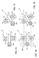
- FIGS. 1A, 1B, 1C and 1D are explanatory drawings of a basic functional configuration.
- FIG. 1A is an essential-part schematic plan view of a normally designed transistor.
- FIG. 1B is an essential-part schematic plan view of a transistor obtained by the manufacturing based on the design of FIG. 1A.
- FIG. 1C is an essential-part schematic plan view of an obliquely configured and designed transistor.
- FIG. 1D is an essential-part schematic plan view of a transistor obtained by the manufacturing based on the design of FIG. 1C.
- a transistor 10 has the following configuration.
- a gate electrode 11 linearly extending in the horizontal direction in the drawing is configured, and active region 12 extending in the direction (gate length direction) perpendicular to a major axis direction of the electrode 11 is configured to intersect the electrode 11.
- contact electrodes 13a, 13b and 13c connected to each of the electrode 11 and regions 12 are configured.
- the configuration of the respective contact electrodes 13b and 13c is determined such that a constant distance (e.g., a distance in a minimum design rule) X is secured between the gate electrode 11 and each of the contact electrodes 13b and 13c on both sides of the gate electrode 11.
- a constant distance e.g., a distance in a minimum design rule
- any of the gate electrode 11, the active region 12 and the contact electrodes 13a, 13b and 13c which are configured (drawn) in a rectangle shape in terms of design are formed to have rounded corners as shown in FIG. 1B.
- the contact electrodes 13a, 13b and 13c have a circular shape depending on sizes thereof.
- the transistor 10 shown in FIG. 1C is a transistor obtained by obliquely designing the transistor 10 shown in FIG. 1A (by designing the transistor 10 obliquely only by an angle of ⁇ ).
- the transistor 10 has the following configuration.
- the gate electrode 11 linearly extending is obliquely configured, and the active region 12 is configured in the direction perpendicular to the major axis direction of the gate electrode 11. Further, on an end of the gate electrode 11 as well as within the active region 12, the contact electrodes 13a, 13b and 13c connected to each of the electrode 11 and regions 12 are configured.
- the rectangular contact electrodes 13a, 13b and 13c are configured (drawn) without being designed obliquely for convenience of design. Therefore, in a stage of design, the gate electrode 11 and each of the contact electrodes 13b and 13c have a configuration relationship in which a distance therebetween is shorter than the distance X shown in FIGS. 1A and 1B.
- the gate electrode 11, active region 12, and contact electrodes 13a, 13b and 13c each having rounded corners are formed as shown in FIG. 1D.
- each of the contact electrodes 13a, 13b and 13c is formed to a round shape. Therefore, between the gate electrode 11 and each of the contact electrodes 13b and 13c having a configuration relationship in which a distance therebetween is shorter than the distance X in a stage of design, a constant distance X is secured after actual formation.
- the transistor 10 in FIG. 1D has a configuration in which the transistor 10 in FIG. 1B is configured obliquely by an angle ⁇ .
- the transistor 10 is manufactured to have a configuration as shown in FIG. 1B, spaces such as regions 14a and 14b exist in terms of the layout.
- the transistor 10 is configured obliquely from a state of FIG. 1B to that of FIG. 1D, such regions 14a and 14b can be efficiently used in terms of the layout.
- a part of the gate electrode 11 and of the active region 12 can be configured using the regions 14a and 14b.
- the center position of the contact electrode 13c is shifted by a distance Y in the downward direction in the drawing.
- size reduction in the vertical direction in the drawing can be realized without reducing the distance X between the gate electrode 11 and each of the contact electrodes 13b and 13c.
- the center position of the contact electrode 13a connected to the gate electrode 11 is shifted by a distance Z in the left direction in the drawing.
- the size reduction effect in the vertical direction in the drawing as shown in FIG. 1 becomes more remarkable when plural transistors are adjacent to each other.
- the transistor 10 When the transistor 10 is included in a specific unit cell, for example, in a unit cell which is long in the horizontal direction in the drawing and is short in the vertical direction in the drawing, the following effect is provided.
- the size reduction effect in the vertical direction in the drawing is apt to be larger than the size increase effect in the horizontal direction in the drawing.
- FIGS. 2 and 3 are explanatory drawings of the size reduction effect in adjacent transistors.
- each of linear gate electrodes 21 and 31 is formed to intersect an active region 40. On ends of the gate electrodes 21 and 31, contact electrodes 21a and 31a are formed, respectively. Within the active region 40, contact electrodes 41a, 41b and 41c are formed.
- FIG. 2 shows a configuration in which one transistor 20 of the adjacent transistors 20 and 30 is configured obliquely by an angle ⁇ from the standard configuration
- This configuration means a configuration in which the transistor 20 is not configured obliquely. In FIG. 2, this configuration is shown by a dotted line.
- the gate electrodes 21 and 31 have a non-parallel configuration relationship.
- the active region 40 has not a linear shape but a curved shape in the region between the gate electrodes 21 and 31.
- FIG. 3 shows a configuration in which both of the adjacent transistors 20 and 30 are configured obliquely by an angle ⁇ in the direction opposite each other away from the standard configuration (This configuration means a configuration in which the transistors 20 and 30 are not configured obliquely. In FIG. 3, this configuration is shown by a dotted line.).
- the gate electrodes 21 and 31 have a non-parallel configuration relationship.
- the active region 40 in the region between the gate electrodes 21 and 31 has a more curved shape than that of FIG. 2.
- the position of the contact electrode 41a can be shifted in the upward direction in the drawing while keeping a distance between the contact electrode 41a and the gate electrode 31. Accordingly, a size S between the adjacent transistors 20 and 30 in the vertical direction in the drawing can be more reduced as compared with that in the standard configuration.
- the angle ⁇ is set in the range of 0° ⁇ 45°.
- the angle ⁇ is more than 45°, the following disadvantages occur. That is, there is an increasing possibility that interference among constituents occurs in terms of the layout. Further, the need to largely change the layout of wirings formed on an upper layer may arise.
- the angle ⁇ is set in the relatively small range of 45° or less, the following advantages are provided. That is, the interference among constituents or the problem in layout change can be avoided. Therefore, no significant difficulty is encountered in obliquely configuring and designing a transistor. Further, no significant difficulty is encountered also in manufacturing a transistor based on the design.
- both of the gate electrode and active region constituting the transistor are configured obliquely by a constant angle ⁇ .
- the following case is possible.
- only the active region or only the gate electrode is obliquely configured in consideration of a distance margin between the gate electrode and the contact electrode.
- a part of the gate electrode e.g., a protruded part from the active region
- a part of the gate electrode is obliquely configured without changing a configuration of an essential-part of the gate electrode as well as a configuration of the active region.
- other transistor constituents can be configured on an empty space formed by obliquely configuring a part of the gate electrode. This point will be described later.
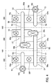
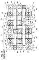
- FIG. 4 is an essential-part schematic plan view of a standard parallel-type SRAM unit cell.
- FIG. 5 is an essential-part schematic plan view of an SRAM unit cell of the first application example.
- a standard SRAM unit cell 50a comprises a total of six transistors composed of load transistors L1 and L2 configured in the central part, driver transistors D1 and D2 and transfer transistors T1 and T2 configured outside of the central part.
- Well region boundaries 161 and 162 have boundaries for injecting different conductivity-type impurities. In the left and right regions of these boundaries, different conductivity-type transistors are configured.
- the driver transistors D1 and D2 and transfer transistors T1 and T2 in the well regions 163 and 165 are configured as an N-type transistor.
- the load transistors L1 and L2 in the well region 164 are configured as a P-type transistor.
- a gate electrode 51 of the load transistor L1 and the driver transistor D1, a gate electrode 52 of the load transistor L2 and the driver transistor D2, and gate electrodes 53 and 54 of the transfer transistors T1 and T2 each have a linear shape in the major axis direction and are configured parallel to each other.
- Active regions 55 , 56, 57 and 58 are extended in the direction perpendicular to the major axis direction of the gate electrodes 51, 52, 53 and 54, respectively.
- the active region 55 is configured to intersect the gate electrode 51.
- the active region 56 is configured to intersect the gate electrode 52.
- the active region 57 is configured to intersect the gate electrodes 51 and 53.
- the active region 58 is configured to intersect the gate electrodes 52 and 54.
- contact electrodes 59a to 591 connected to each of the gate electrodes and active regions are configured.
- Both of the contact electrodes 59a and 59d of the load transistors L1 and L2 are connected to a power supply line Vcc in the upper layer. That is, sources of the load transistors L1 and L2 are connected to the power supply line Vcc.
- Both of the contact electrodes 59e and 59j of the driver transistors D1 and D2 are connected to a grounding line Vss in the upper layer. That is, sources of the driver transistors D1 and D2 are connected to the grounding line Vss.
- the contact electrode 59g of the transfer transistor T1 is connected to a first bit line BL1 in the upper layer, and the contact electrode 59h of the transfer transistor T2 is connected to a second bit line BL2 in the upper layer. That is, a source of the transfer transistor T1 is connected to the first bit line BL1, and a source of the transfer transistor T2 is connected to the second bit line BL2.
- the contact electrodes 59k and 591 connected to the gate electrodes 53 and 54 of the transfer transistors T1 and T2 are connected to a common word line WL in the upper layer.
- a shared contact technology is applied to the contact electrodes 59b and 59c connected to the gate electrodes 52 and 51.
- the contact electrode 59b is connected to the contact electrode 59f in the upper layer
- the contact electrode 59c is connected to the contact electrode 59i in the upper layer.
- the gate electrode 52 of the load transistor L2 and the driver transistor D2 is connected to each drain of the load transistor L1, the driver transistor D1 and the transfer transistor T1.
- the gate electrode 51 of the load transistor L1 and the driver transistor D1 is connected to each drain of the load transistor L2, the driver transistor D2 and the transfer transistor T2.
- an SRAM unit cell 50 shown in FIG. 5 has the following configuration. That is, the transfer transistors T1 and T2 are configured obliquely in the counterclockwise direction in the drawing without changing an electrical connection relationship among constituents (see FIG. 2).
- the SRAM unit cell 50 shown in FIG. 5 has the following configuration. That is, accompanying such miniaturization of outside portions, a distance between the load transistors L1 and L2 in the central part is reduced as compared with that in the SRAM unit cell 50a shown in FIG. 4.
- sizes of the active regions 55 and 56 are appropriately changed to bring the gate electrode 51 and the contact electrode 59c closer to the gate electrode 52 side or to bring the gate electrode 52 and the contact electrode 59b closer to the gate electrode 51 side.
- a space allowing such a configuration change to be performed is left even in the standard configuration.
- the size reduction in the outside portion namely, the size reduction in the transfer transistor T1 and driver transistor D1 in the vertical direction in the drawing as well as in the transfer transistor T2 and driver transistor D2 in the vertical direction in the drawing is performed. Further, a distance between the load transistors L1 and L2 is reduced such that the contact electrodes 59a, 59e and 59h as well as the contact electrodes 59d, 59g and 59j are configured on the cell boundary line and at the same time, the gate electrodes 51 and 52 are configured parallel to each other.
- a size in the short-side direction (in the vertical direction in the drawing) of the SRAM unit cell 50 shown in FIG. 5, which is viewed as a cell having a planar rectangular shape, can be reduced as compared with that in the SRAM unit cell 50a shown in FIG. 4.
- wirings connected to the contact electrodes in the upper layer may be configured according to oblique angles of the transfer transistors T1 and T2 while undergoing a parallel movement from positions in the case of not configuring the transistors T1 and T2 obliquely. This is also true for the first and second bit lines BL1 and BL2, and the word line WL. Accordingly, in configuring the SRAM unit cell 60 as shown in FIG. 5, a large design change is unnecessary for the wiring structure of the upper layer.
- FIG. 6 is an essential-part schematic plan view of an SRAM unit cell of the second application example.
- the same elements as those shown in FIGS. 4 and 5 are indicated by the same reference numerals as in FIGS. 4 and 5 and the detailed description is omitted.
- an SRAM unit cell 60 shown in FIG. 6 has the following configuration. That is, the load transistors L1 and L2 are configured obliquely in the counterclockwise direction in the drawing without changing an electrical connection relationship among constituents. At this time, the gate electrodes 61 and 62 are formed in a shape corresponding to the configuration relationship between the driver transistor D1 and the obliquely configured load transistor L1 as well as between the driver transistor D2 and the obliquely configured load transistor L2, respectively. A distance between the load transistors L1 and L2 is set such that the contact electrodes 59a, 59e and 59h as well as the contact electrodes 59d, 59g and 59j are configured on the cell boundary line.
- the SRAM unit cell 60 shown in FIG. 6 has the following configuration. That is, the driver transistor D1 and the transfer transistor T1 as well as the driver transistor D2 and the transfer transistor T2 are configured closer to the load transistor L1 and L2 sides, respectively, than those of the standard configuration.
- the load transistors L1 and L2 in the central part are configured obliquely.
- new spaces can be formed with the outer driver transistor D1 and transfer transistor T1 as well as with the outer driver transistor D2 and transfer transistor T2.
- the driver transistors D1 and D2 as well as the transfer transistors T1 and T2 are configured. By doing so, the size in the horizontal direction in the drawing can be reduced as compared with that in the SRAM unit cell 50a shown in FIG. 4. As a result, the cell area can be reduced.
- FIG. 7 is an essential-part schematic plan view of the SRAM unit cell of the third application example.
- the same elements as those shown in FIGS. 4 and 5 are indicated by the same reference numerals as in FIGS. 4 and 5 and the detailed description is omitted.
- an SRAM unit cell 70 shown in FIG. 7 has the following configuration. That is, without changing an electrical connection relationship among constituents, the transfer transistors T1 and T2 are configured obliquely in the counterclockwise direction in the drawing as well as the load transistors L1 and L2 are configured obliquely in the counterclockwise direction in the drawing. Further, using spaces formed by configuring obliquely the load transistors L1 and L2, the driver transistors D1 and D2 as well as the transfer transistors T1 and T2 are configured.
- the gate electrodes 71 and 72 are formed in a shape corresponding to the configuration relationship between the driver transistor D1 and the obliquely configured load transistor L1 as well as between the driver transistor D2 and the obliquely configured load transistor L2, respectively.
- a distance between the load transistors L1 and L2 is set such that the contact electrodes 59a, 59e and 59h as well as the contact electrodes 59d, 59g and 59j are configured on the cell boundary line.
- the size reduction in the vertical direction in the drawing is realized by obliquely configuring the transfer transistors T1 and T2.
- the size reduction in the horizontal direction in the drawing is realized by obliquely configuring the load transistors L1 and L2.
- the cell area is reduced.
- FIG. 8 is an essential-part schematic plan view of the SRAM unit cell of the fourth application example.
- the same elements as those shown in FIGS. 4 and 5 are indicated by the same reference numerals as in FIGS. 4 and 5 and the detailed description is omitted.
- an SRAM unit cell 80 shown in FIG. 8 has the following configuration. That is, without changing an electrical connection relationship among constituents, the transfer transistors T1 and T2 are configured obliquely in the counterclockwise direction in the drawing as well as the driver transistors D1 and D2 are configured obliquely in the clockwise direction in the drawing (see FIG. 3).
- the gate electrodes 81 and 82 are formed in a shape corresponding to the configuration relationship between the obliquely configured driver transistor D1 and the load transistor L1 as well as between the obliquely configured driver transistor D2 and the load transistor L2, respectively.
- the SRAM unit cell 80 shown in FIG. 8 has the following configuration. That is, as compared with the case in the SRAM unit cell 50a shown in FIG. 4, a distance between the load transistors L1 and L2 is reduced such that the contact electrodes 59a, 59e and 59h as well as the contact electrodes 59d, 59g and 59j are configured on the cell boundary line.
- the transfer transistors T1 and T2 and the driver transistors D1 and D2 are each configured obliquely in the predetermined direction and the distance between the load transistors L1 and L2 is reduced, whereby the size reduction in the vertical direction in the drawing is realized . Therefore, even if a size in the long-side direction of the rectangular SRAM unit cell 80 slightly increases, a size in the short-side direction thereof is reduced. As a result, the cell area can be effectively reduced.
- FIG. 9 is an essential-part schematic plan view of an SRAM unit cell of the fifth application example.
- the same elements as those shown in FIGS. 4 and 5 are indicated by the same reference numerals as in FIGS. 4 and 5 and the detailed description is omitted.
- an SRAM unit cell 90 shown in FIG. 9 has the following configuration. That is, without changing an electrical connection relationship among constituents, the transfer transistors T1 and T2 are configured obliquely in the counterclockwise direction in the drawing, the driver transistors D1 and D2 are configured obliquely in the clockwise direction in the drawing and at the same time, the load transistors L1 and L2 are configured obliquely in the counterclockwise direction in the drawing. Further, using spaces formed by obliquely configuring the load transistors L1 and L2, the driver transistors D1 and D2 as well as the transfer transistors T1 and T2 are configured.
- the gate electrodes 91 and 92 are formed in a shape corresponding to the configuration relationship between the obliquely configured driver transistor D1 and load transistor L1 as well as between the obliquely configured driver transistor D2 and load transistor L2, respectively.
- a distance between the load transistors L1 and L2 is set such that the contact electrodes 59a, 59e and 59h as well as the contact electrodes 59d, 59g and 59j are configured on the cell boundary line.
- the size reduction in the vertical direction in the drawing is realized by obliquely configuring the transfer transistors T1 and T2 and the driver transistors D1 and D2.
- the size reduction in the horizontal direction in the drawing is realized by obliquely configuring the load transistors L1 and L2. As a result, the cell area is reduced.
- the cell area reduction of at least about 5% can be realized as compared with that in the SRAM unit cell 50a shown in FIG. 4.
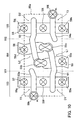
- FIG. 10 is an essential-part schematic plan view of an SRAM unit cell of the sixth application example.
- the same elements as those shown in FIG. 6 are indicated by the same reference numerals as in FIG. 6 and the detailed description is omitted.
- An SRAM unit cell 60a shown in FIG. 10 has the following configuration. That is, ends of the gate electrodes 53a and 54a of the transfer transistors T1 and T2 are configured obliquely in the direction apart from the contact electrodes 59b and 59c, respectively. In this point, the SRAM unit cell 60a differs from the SRAM unit cell 60 of the second application example shown in FIG. 6.
- the driver transistor D1 and the transfer transistor T1 as well as the driver transistor D2 and the transfer transistor T2 are configured closer to the load transistor L1 and L2 sides while securing a distance margin between the end of the gate electrode 53a and the contact electrode 59b as well as between the end of the gate electrode 54a and the contact electrode 59c, respectively.
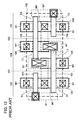
- FIG. 11 is an essential-part schematic plan view of an SRAM unit cell of the seventh application example.
- the same elements as those shown in FIG. 6 are indicated by the same reference numerals as in FIG. 6 and the detailed description is omitted.
- An SRAM unit cell 60b shown in FIG. 11 has the following configuration. That is, all of the gate electrodes 53b and 54b of the transfer transistors T1 and T2 are configured obliquely in the direction apart from the contact electrodes 59b and 59c, respectively. In this point, the SRAM unit cell 60b differs from the SRAM unit cell 60 of the second application example shown in FIG. 6.
- the driver transistor D1 and the transfer transistor T1 as well as the driver transistor D2 and the transfer transistor T2 are configured closer to the load transistor L1 and L2 sides while securing a distance margin between the end of the gate electrode 53a and the contact electrode 59b as well as between the end of the gate electrode 54a and the contact electrode 59c, respectively.
- the parallel-type unit cell having each pair of the load transistors, the driver transistors and the transfer transistors at least any one of the pairs of the transistors is configured obliquely from the standard configuration.
- a constant distance for example, a minimum rule distance in design and in processing is secured between the gate electrode and the contact electrode formed in the active region.
- the parallel-type unit cell having each pair of the load transistors, the driver transistors and the transfer transistors at least any one of the pairs of the transistors is configured obliquely from the standard configuration.
Landscapes
- Semiconductor Memories (AREA)
Abstract
Description
- The present invention relates to a semiconductor memory device. More particularly, the present invention relates to a static-type semiconductor memory device.
- A Static Random Access Memory (SRAM) as one type of volatile memory requires no refresh operation and has a high operation speed. Therefore, the SRAM is currently used in various devices. In recent years, higher speed up, miniaturization of unit cells and improvement in a degree of integration have progressed. Therefore, applications of the SRAM have more spread.
- Herein, one example of conventional SRAM unit cells will be described with reference to FIGS. 12 to 15. FIGS. 12 to 15 illustrate by an example an SRAM unit cell including a bulk layer having formed thereon a transistor and including first to third wiring layers sequentially formed on the bulk layer.
- FIG. 12 is an essential-part schematic plan view between a bulk layer and a first wiring layer of a conventional SRAM unit cell. FIG. 13 is an essential-part schematic plan view between a bulk layer and a second wiring layer of a conventional SRAM unit cell. FIG. 14 is an essential-part schematic plan view between a bulk layer and a third wiring layer of a conventional SRAM unit cell. FIG. 15 is an equivalent circuit diagram of an SRAM unit cell.
- An
SRAM unit cell 100 comprises a total of six transistors composed of load transistors L1 and L2, driver transistors D1 and D2, and transfer transistors T1 and T2. - These six transistors have the following configuration. For example, as shown in FIG. 12, a
gate electrode 101 of the load transistor L1 and the driver transistor D1, agate electrode 102 of the load transistor L2 and the driver transistor D2, andgate electrodes region boundaries well regions well region 154, respectively. -
Active regions gate electrodes active regions gate electrodes active region 107 is configured to intersect thegate electrodes active region 108 is configured to intersect thegate electrodes - On ends of the
respective gate electrodes active regions respective gate electrodes gate electrode 101 of the load transistor L1 as well as within theactive region 106 of the load transistor L2, for example, the contact electrodes using a shared contact technology are configured. Similarly, on thegate electrode 102 of the load transistor L2 as well as within theactive region 105 of the load transistor L1, for example, the contact electrodes using a shared contact technology are configured. - Each of the
gate electrodes active regions - Each of the respective first wirings M1 is further connected to a second wiring M2 (dotted line in the drawing) through the contact electrode, as shown in FIG. 13. Among these, the second wiring M2 for connecting between the first wirings M1 connected to the
gate electrodes - Each of the respective second wirings M2 is further connected to a third wiring M3 (dashed line in the drawing) through the contact electrode, as shown in FIG. 14. Through the third wiring, the load transistors L1 and L2 are connected to a power supply line Vcc, the driver transistors D1 and D2 are connected to a grounding line Vss and the transfer transistors T1 and T2 are connected to the bit lines BL1 and BL2, respectively.
- As a result, a circuit as shown in FIG. 15 is realized.
- Thus, the conventional SRAM unit cell generally has the following configuration. That is, the gate electrodes each have a linear shape and are configured parallel to each other. Further, the active regions are each extended linearly in the direction perpendicular to the gate electrodes and are configured parallel to each other. The SRAM unit cell using such a configuration is called as a "parallel-type unit cell" and has a merit that design and manufacture (process) are easy. In addition to the above merit, the unit cell further has a merit that by configuring the respective transistors in an orderly manner, reduction in a unit cell area and improvement in a degree of integration can be realized.
- In the SRAM, further miniaturization of the unit cell is now desired strongly with spreading of its application and a demand for its large capacity.
- In order to realize miniaturization of the SRAM, a SRAM unit cell having various configurations is recently proposed. For example, there is proposed the following SRAM unit cell. Gate electrodes and active regions are configured parallel to each other, respectively. Further, the gate electrodes and the active regions are configured obliquely to a word line and to bit line perpendicular thereto. Thus, the area reduction in the SRAM unit cell is realized (see, e.g.,
Japanese Unexamined Patent Application Publication No. Hei 10-335487 Japanese Unexamined Patent Application Publication No. Hei 6-169071 Japanese Unexamined Patent Application Publication No. Hei 8-97298 - In the case of a parallel-type SRAM unit cell heretofore widely used, area reduction thereof can be realized by using the following configuration. For example, gate electrodes and active regions are configured parallel to each other, respectively. At the same time, a distance therebetween is reduced within a technically-feasible range.
- However, the following problems now occur upon a further miniaturization request of an SRAM unit cell. That is, it becomes difficult to reduce the unit cell area while securing a distance margin between a gate electrode of each transistor and a contact electrode connected to an active region of each transistor.
- Further, it becomes difficult to secure the distance margin between constituents of different transistors only by simply reducing a distance between gate electrodes or between active regions. For example, in the above-described parallel-type SRAM unit cell, it becomes difficult to secure the distance margin between a gate electrode end of a transfer transistor and a shared contact electrode of a load transistor.
- Therefore, one possible object is to provide a semiconductor memory device having a high-reliable and small unit cell.
- In particular, an example embodiment of the improved semiconductor memory device includes a unit cell including first and second load transistors configured in a central part and including a first driver transistor and a first transfer transistor as well as a second driver transistor and a second transfer transistor configured on each side of the central part, wherein: using as a standard configuration a cell configuration in which a first gate electrode of the first load transistor and the first driver transistor, a second gate electrode of the second load transistor and the second driver transistor, a third gate electrode of the first transfer transistor, the third gate electrode being configured in a major axis direction of the second gate electrode, and a fourth gate electrode of the second transfer transistor, the fourth gate electrode being configured in a major axis direction of the first gate electrode, each have a linear shape and are configured parallel to each other, and first and second active regions each having formed therein the first and second gate electrodes, a third active region having formed therein the first and third gate electrodes, and a fourth active region having formed therein the second and fourth gate electrodes are each extended linearly in the direction perpendicular to the major axis direction of the first to fourth gate electrodes and are configured parallel to each other, gate electrodes and active regions of at least any one of the pairs of transistors selected from a pair of the first and second load transistors, a pair of the first and second driver transistors, and a pair of the first and second transfer transistors are configured obliquely from the standard configuration.
- The above and other objects, features and advantages of the present invention will become apparent from the following description when taken in conjunction with the accompanying drawings which illustrate preferred embodiments of the present invention by way of example.
-
- FIGS. 1A, 1B, 1C and 1D are explanatory drawings of a basic functional configuration. FIG. 1A is an essential-part schematic plan view of a normally designed transistor. FIG. 1B is an essential-part schematic plan view of a transistor obtained by the manufacturing based on the design of FIG. 1A. FIG. 1C is an essential-part schematic plan view of an obliquely configured and designed transistor. FIG. 1D is an essential-part schematic plan view of a transistor obtained by the manufacturing based on the design of FIG. 1C.
- FIG. 2 is an explanatory drawing of a size reduction effect in adjacent transistors (part 1).
- FIG. 3 is an explanatory drawing of a size reduction effect in adjacent transistors (part 2).
- FIG. 4 is an essential-part schematic plan view of a standard parallel-type SRAM unit cell.
- FIG. 5 is an essential-part schematic plan view of an SRAM unit cell of a first application example.
- FIG. 6 is an essential-part schematic plan view of an SRAM unit cell of a second application example.
- FIG. 7 is an essential-part schematic plan view of an SRAM unit cell of a third application example.
- FIG. 8 is an essential-part schematic plan view of an SRAM unit cell of a fourth application example.
- FIG. 9 is an essential-part schematic plan view of an SRAM unit cell of a fifth application example.
- FIG. 10 is an essential-part schematic plan view of an SRAM unit cell of a sixth application example.
- FIG. 11 is an essential-part schematic plan view of an SRAM unit cell of a seventh application example.
- FIG. 12 is an essential-part schematic plan view between a bulk layer and a first wiring layer of a conventional SRAM unit cell.
- FIG. 13 is an essential-part schematic plan view between a bulk layer and a second wiring layer of a conventional SRAM unit cell.
- FIG. 14 is an essential-part schematic plan view between a bulk layer and a third wiring layer of a conventional SRAM unit cell.
- FIG. 15 is an equivalent circuit diagram of an SRAM unit cell.
- Preferred embodiments of the present invention will be described in detail below with reference to the accompanying drawings, wherein like reference numerals refer to like elements throughout.
- FIGS. 1A, 1B, 1C and 1D are explanatory drawings of a basic functional configuration. FIG. 1A is an essential-part schematic plan view of a normally designed transistor. FIG. 1B is an essential-part schematic plan view of a transistor obtained by the manufacturing based on the design of FIG. 1A. FIG. 1C is an essential-part schematic plan view of an obliquely configured and designed transistor. FIG. 1D is an essential-part schematic plan view of a transistor obtained by the manufacturing based on the design of FIG. 1C.
- As shown in FIG. 1A, a
transistor 10 has the following configuration. Agate electrode 11 linearly extending in the horizontal direction in the drawing is configured, andactive region 12 extending in the direction (gate length direction) perpendicular to a major axis direction of theelectrode 11 is configured to intersect theelectrode 11. Further, on an end of thegate electrode 11 as well as within theactive regions 12 on both sides of theelectrode 11,contact electrodes electrode 11 andregions 12 are configured. - In designing such a
transistor 10, the configuration of therespective contact electrodes gate electrode 11 and each of thecontact electrodes gate electrode 11. - This is because when the constant distance X is not secured, the following problem occurs. In actually performing manufacturing based on the design, when displacement occurs in a formed position of the
gate electrode 11 or in a formed position of a contact hole, a short circuit may occur between thegate electrode 11 and each of thecontact electrodes contact electrodes gate electrode 11. - When actually performing manufacturing based on such a design, any of the
gate electrode 11, theactive region 12 and thecontact electrodes contact electrodes - On the other hand, the
transistor 10 shown in FIG. 1C is a transistor obtained by obliquely designing thetransistor 10 shown in FIG. 1A (by designing thetransistor 10 obliquely only by an angle of θ). Thetransistor 10 has the following configuration. Thegate electrode 11 linearly extending is obliquely configured, and theactive region 12 is configured in the direction perpendicular to the major axis direction of thegate electrode 11. Further, on an end of thegate electrode 11 as well as within theactive region 12, thecontact electrodes electrode 11 andregions 12 are configured. - In the case of obliquely configuring and designing the
transistor 10, therectangular contact electrodes gate electrode 11 and each of thecontact electrodes - When actually performing manufacturing based on the design of FIG. 1C, the
gate electrode 11,active region 12, andcontact electrodes contact electrodes gate electrode 11 and each of thecontact electrodes - Herein, configurations of the
transistors 10 shown in FIGS. 1B and 1D are compared. - Comparing FIGS. 1B and 1D, the
transistor 10 in FIG. 1D has a configuration in which thetransistor 10 in FIG. 1B is configured obliquely by an angle θ. However, when thetransistor 10 is manufactured to have a configuration as shown in FIG. 1B, spaces such asregions transistor 10 is configured obliquely from a state of FIG. 1B to that of FIG. 1D,such regions - Specifically, when the
transistor 10 is configured obliquely from a state of FIG. 1B to that of FIG. 1D on the basis of a center position of thecontact electrode 13b, a part of thegate electrode 11 and of theactive region 12 can be configured using theregions contact electrode 13c is shifted by a distance Y in the downward direction in the drawing. As a result, size reduction in the vertical direction in the drawing can be realized without reducing the distance X between thegate electrode 11 and each of thecontact electrodes - When the
transistor 10 is thus configured obliquely, the center position of thecontact electrode 13a connected to thegate electrode 11 is shifted by a distance Z in the left direction in the drawing. - The size reduction effect in the vertical direction in the drawing as shown in FIG. 1 becomes more remarkable when plural transistors are adjacent to each other.
- When the
transistor 10 is included in a specific unit cell, for example, in a unit cell which is long in the horizontal direction in the drawing and is short in the vertical direction in the drawing, the following effect is provided. When making a comparison in terms of areas, even if the size in the horizontal direction in the drawing increases, the size reduction effect in the vertical direction in the drawing is apt to be larger than the size increase effect in the horizontal direction in the drawing. - FIGS. 2 and 3 are explanatory drawings of the size reduction effect in adjacent transistors.
- For example, assume that two
transistors transistors linear gate electrodes active region 40. On ends of thegate electrodes contact electrodes active region 40,contact electrodes - FIG. 2 shows a configuration in which one
transistor 20 of theadjacent transistors transistor 20 is not configured obliquely. In FIG. 2, this configuration is shown by a dotted line.). At this time, thegate electrodes active region 40 has not a linear shape but a curved shape in the region between thegate electrodes contact electrode 41c can be shifted in the downward direction in the drawing while keeping a distance between thecontact electrode 41c and thegate electrode 21. Accordingly, a size S between theadjacent transistors - FIG. 3 shows a configuration in which both of the
adjacent transistors transistors gate electrodes active region 40 in the region between thegate electrodes contact electrode 41c can be shifted in the downward direction in the drawing while keeping a distance between thecontact electrode 41c and thegate electrode 21. At the same time, the position of thecontact electrode 41a can be shifted in the upward direction in the drawing while keeping a distance between thecontact electrode 41a and thegate electrode 31. Accordingly, a size S between theadjacent transistors - As described above, by adopting a configuration in which the transistor is configured obliquely by a constant angle θ from the standard configuration, size reduction in a predetermined direction can be realized while securing a distance margin between the gate electrode and the contact electrode.
- Herein, the angle θ is set in the range of 0°<θ≤45°. When the angle θ is more than 45°, the following disadvantages occur. That is, there is an increasing possibility that interference among constituents occurs in terms of the layout. Further, the need to largely change the layout of wirings formed on an upper layer may arise. When the angle θ is set in the relatively small range of 45° or less, the following advantages are provided. That is, the interference among constituents or the problem in layout change can be avoided. Therefore, no significant difficulty is encountered in obliquely configuring and designing a transistor. Further, no significant difficulty is encountered also in manufacturing a transistor based on the design.
- In the above description, there is described a case where the whole one transistor, more specifically, both of the gate electrode and active region constituting the transistor are configured obliquely by a constant angle θ. In addition, the following case is possible. In one transistor, only the active region or only the gate electrode is obliquely configured in consideration of a distance margin between the gate electrode and the contact electrode.
- In the case where only the active region is obliquely configured in consideration of a distance margin between the gate electrode and the contact electrode, size reduction in the direction perpendicular to the major axis direction of the gate electrode can be realized according to the above example.
- In the case where only the gate electrode is obliquely configured in consideration of a distance margin between the gate electrode and the contact electrode, size reduction can be realized depending on the configuration of the transistor. Further, other transistor constituents can also be configured on an empty space formed by obliquely configuring the gate electrode. This point will be described later.
- Further, the following case is also possible. In one transistor, only a part of the gate electrode (e.g., a protruded part from the active region) is obliquely configured without changing a configuration of an essential-part of the gate electrode as well as a configuration of the active region. Also in this case, other transistor constituents can be configured on an empty space formed by obliquely configuring a part of the gate electrode. This point will be described later.
- A case of applying the above-described principle to an SRAM will be described in detail below.
- A first application example will be first described.
- FIG. 4 is an essential-part schematic plan view of a standard parallel-type SRAM unit cell. FIG. 5 is an essential-part schematic plan view of an SRAM unit cell of the first application example.
- First, a standard cell configuration (standard configuration) will be described with reference to FIG. 4.
- As shown in FIG. 4, a standard
SRAM unit cell 50a comprises a total of six transistors composed of load transistors L1 and L2 configured in the central part, driver transistors D1 and D2 and transfer transistors T1 and T2 configured outside of the central part. Wellregion boundaries well regions well region 164 are configured as a P-type transistor. - These six transistors have the following configuration. A
gate electrode 51 of the load transistor L1 and the driver transistor D1, agate electrode 52 of the load transistor L2 and the driver transistor D2, andgate electrodes -
Active regions gate electrodes active region 55 is configured to intersect thegate electrode 51. Theactive region 56 is configured to intersect thegate electrode 52. Theactive region 57 is configured to intersect thegate electrodes active region 58 is configured to intersect thegate electrodes - On ends of the
respective gate electrodes active regions respective gate electrodes contact electrodes 59a to 591 connected to each of the gate electrodes and active regions are configured. - Both of the
contact electrodes - Both of the
contact electrodes - The
contact electrode 59g of the transfer transistor T1 is connected to a first bit line BL1 in the upper layer, and thecontact electrode 59h of the transfer transistor T2 is connected to a second bit line BL2 in the upper layer. That is, a source of the transfer transistor T1 is connected to the first bit line BL1, and a source of the transfer transistor T2 is connected to the second bit line BL2. - The
contact electrodes gate electrodes - A shared contact technology is applied to the
contact electrodes gate electrodes contact electrode 59b is connected to thecontact electrode 59f in the upper layer, and thecontact electrode 59c is connected to thecontact electrode 59i in the upper layer. In other words, thegate electrode 52 of the load transistor L2 and the driver transistor D2 is connected to each drain of the load transistor L1, the driver transistor D1 and the transfer transistor T1. Further, thegate electrode 51 of the load transistor L1 and the driver transistor D1 is connected to each drain of the load transistor L2, the driver transistor D2 and the transfer transistor T2. - As a result, a circuit as shown in FIG. 15 is realized.
- When a cell configuration of the
SRAM unit cell 50a as shown in FIG. 4 is used as a standard configuration, anSRAM unit cell 50 shown in FIG. 5 has the following configuration. That is, the transfer transistors T1 and T2 are configured obliquely in the counterclockwise direction in the drawing without changing an electrical connection relationship among constituents (see FIG. 2). - Therefore, sizes in the transfer transistor T1 and driver transistor D1 in the vertical direction in the drawing as well as sizes in the transfer transistor T2 and driver transistor D2 in the vertical direction in the drawing are reduced as compared with those in the standard configuration.
- Further, the
SRAM unit cell 50 shown in FIG. 5 has the following configuration. That is, accompanying such miniaturization of outside portions, a distance between the load transistors L1 and L2 in the central part is reduced as compared with that in theSRAM unit cell 50a shown in FIG. 4. - Specifically, sizes of the
active regions gate electrode 51 and thecontact electrode 59c closer to thegate electrode 52 side or to bring thegate electrode 52 and thecontact electrode 59b closer to thegate electrode 51 side. Between thegate electrode 51 and thecontact electrode 59b as well as between thegate electrode 52 and thecontact electrode 59c, a space allowing such a configuration change to be performed is left even in the standard configuration. - Thus, the size reduction in the outside portion, namely, the size reduction in the transfer transistor T1 and driver transistor D1 in the vertical direction in the drawing as well as in the transfer transistor T2 and driver transistor D2 in the vertical direction in the drawing is performed. Further, a distance between the load transistors L1 and L2 is reduced such that the
contact electrodes contact electrodes gate electrodes - By adopting such a configuration, a size in the short-side direction (in the vertical direction in the drawing) of the
SRAM unit cell 50 shown in FIG. 5, which is viewed as a cell having a planar rectangular shape, can be reduced as compared with that in theSRAM unit cell 50a shown in FIG. 4. - At this time, a size in the long-side direction (in the horizontal direction in the drawing) increases slightly. However, since the
SRAM unit cell 50 has a long rectangular shape in the horizontal direction in the drawing, the amount of reduction in the cell area due to the size reduction in the short-side direction exceeds the amount of increase in the cell area due to the size increase in the long-side direction. As a result, reduction in the cell area can be realized. - Even in the case of thus configuring obliquely the transfer transistors T1 and T2, displacement in the
contact electrodes active regions contact electrodes gate electrodes SRAM unit cell 60 as shown in FIG. 5, a large design change is unnecessary for the wiring structure of the upper layer. - Next, a second application example will be described.
- FIG. 6 is an essential-part schematic plan view of an SRAM unit cell of the second application example. In FIG. 6, the same elements as those shown in FIGS. 4 and 5 are indicated by the same reference numerals as in FIGS. 4 and 5 and the detailed description is omitted.
- When a cell configuration of the
SRAM unit cell 50a as shown in FIG. 4 is used as a standard configuration, anSRAM unit cell 60 shown in FIG. 6 has the following configuration. That is, the load transistors L1 and L2 are configured obliquely in the counterclockwise direction in the drawing without changing an electrical connection relationship among constituents. At this time, thegate electrodes contact electrodes contact electrodes - Further, the
SRAM unit cell 60 shown in FIG. 6 has the following configuration. That is, the driver transistor D1 and the transfer transistor T1 as well as the driver transistor D2 and the transfer transistor T2 are configured closer to the load transistor L1 and L2 sides, respectively, than those of the standard configuration. - Thus, in the
SRAM unit cell 60 shown in FIG. 6, the load transistors L1 and L2 in the central part are configured obliquely. By doing so, as compared with the case where the transistors L1 and L2 are not configured obliquely, new spaces can be formed with the outer driver transistor D1 and transfer transistor T1 as well as with the outer driver transistor D2 and transfer transistor T2. - Further, using the empty spaces, the driver transistors D1 and D2 as well as the transfer transistors T1 and T2 are configured. By doing so, the size in the horizontal direction in the drawing can be reduced as compared with that in the
SRAM unit cell 50a shown in FIG. 4. As a result, the cell area can be reduced. - In configuring the
SRAM unit cell 60 shown in FIG. 6, a large design change is unnecessary for the wiring structure of the upper layer. - Next, a third application example will be described.
- FIG. 7 is an essential-part schematic plan view of the SRAM unit cell of the third application example. In FIG. 7, the same elements as those shown in FIGS. 4 and 5 are indicated by the same reference numerals as in FIGS. 4 and 5 and the detailed description is omitted.
- When a cell configuration of the
SRAM unit cell 50a as shown in FIG. 4 is used as a standard configuration, anSRAM unit cell 70 shown in FIG. 7 has the following configuration. That is, without changing an electrical connection relationship among constituents, the transfer transistors T1 and T2 are configured obliquely in the counterclockwise direction in the drawing as well as the load transistors L1 and L2 are configured obliquely in the counterclockwise direction in the drawing. Further, using spaces formed by configuring obliquely the load transistors L1 and L2, the driver transistors D1 and D2 as well as the transfer transistors T1 and T2 are configured. - The
gate electrodes contact electrodes contact electrodes - Thus, in the
SRAM unit cell 70 shown in FIG. 7, the size reduction in the vertical direction in the drawing is realized by obliquely configuring the transfer transistors T1 and T2. At the same time, the size reduction in the horizontal direction in the drawing is realized by obliquely configuring the load transistors L1 and L2. As a result, the cell area is reduced. - In configuring the
SRAM unit cell 70 shown in FIG. 7, a large design change is unnecessary for the wiring structure of the upper layer. - Next, a fourth application example will be described.
- FIG. 8 is an essential-part schematic plan view of the SRAM unit cell of the fourth application example. In FIG. 8, the same elements as those shown in FIGS. 4 and 5 are indicated by the same reference numerals as in FIGS. 4 and 5 and the detailed description is omitted.
- When a cell configuration of the
SRAM unit cell 50a as shown in FIG. 4 is used as a standard configuration, anSRAM unit cell 80 shown in FIG. 8 has the following configuration. That is, without changing an electrical connection relationship among constituents, the transfer transistors T1 and T2 are configured obliquely in the counterclockwise direction in the drawing as well as the driver transistors D1 and D2 are configured obliquely in the clockwise direction in the drawing (see FIG. 3). - The
gate electrodes SRAM unit cell 80 shown in FIG. 8 has the following configuration. That is, as compared with the case in theSRAM unit cell 50a shown in FIG. 4, a distance between the load transistors L1 and L2 is reduced such that thecontact electrodes contact electrodes - Thus, in the
SRAM unit cell 80 shown in FIG. 8, the transfer transistors T1 and T2 and the driver transistors D1 and D2 are each configured obliquely in the predetermined direction and the distance between the load transistors L1 and L2 is reduced, whereby the size reduction in the vertical direction in the drawing is realized . Therefore, even if a size in the long-side direction of the rectangularSRAM unit cell 80 slightly increases, a size in the short-side direction thereof is reduced. As a result, the cell area can be effectively reduced. - In configuring the
SRAM unit cell 80 shown in FIG. 8, a large design change is unnecessary for the wiring structure of the upper layer. - Next, a fifth application example will be described.
- FIG. 9 is an essential-part schematic plan view of an SRAM unit cell of the fifth application example. In FIG. 9, the same elements as those shown in FIGS. 4 and 5 are indicated by the same reference numerals as in FIGS. 4 and 5 and the detailed description is omitted.
- When a cell configuration of the
SRAM unit cell 50a as shown in FIG. 4 is used as a standard configuration, anSRAM unit cell 90 shown in FIG. 9 has the following configuration. That is, without changing an electrical connection relationship among constituents, the transfer transistors T1 and T2 are configured obliquely in the counterclockwise direction in the drawing, the driver transistors D1 and D2 are configured obliquely in the clockwise direction in the drawing and at the same time, the load transistors L1 and L2 are configured obliquely in the counterclockwise direction in the drawing. Further, using spaces formed by obliquely configuring the load transistors L1 and L2, the driver transistors D1 and D2 as well as the transfer transistors T1 and T2 are configured. - The
gate electrodes contact electrodes contact electrodes - Thus, in the
SRAM unit cell 90 shown in FIG. 9, the size reduction in the vertical direction in the drawing is realized by obliquely configuring the transfer transistors T1 and T2 and the driver transistors D1 and D2. At the same time, the size reduction in the horizontal direction in the drawing is realized by obliquely configuring the load transistors L1 and L2. As a result, the cell area is reduced. - In the case of the
SRAM unit cell 90 shown in FIG. 9, the cell area reduction of at least about 5% can be realized as compared with that in theSRAM unit cell 50a shown in FIG. 4. - In configuring the
SRAM unit cell 90 shown in FIG. 9, a large design change is unnecessary for the wiring structure of the upper layer. - Next, a sixth application example will be described.
- FIG. 10 is an essential-part schematic plan view of an SRAM unit cell of the sixth application example. In FIG. 10, the same elements as those shown in FIG. 6 are indicated by the same reference numerals as in FIG. 6 and the detailed description is omitted.
- An
SRAM unit cell 60a shown in FIG. 10 has the following configuration. That is, ends of thegate electrodes contact electrodes SRAM unit cell 60a differs from theSRAM unit cell 60 of the second application example shown in FIG. 6. - According to the above-described
SRAM unit cell 60a, the driver transistor D1 and the transfer transistor T1 as well as the driver transistor D2 and the transfer transistor T2 are configured closer to the load transistor L1 and L2 sides while securing a distance margin between the end of thegate electrode 53a and thecontact electrode 59b as well as between the end of thegate electrode 54a and thecontact electrode 59c, respectively. - Next, a seventh application example will be described.
- FIG. 11 is an essential-part schematic plan view of an SRAM unit cell of the seventh application example. In FIG. 11, the same elements as those shown in FIG. 6 are indicated by the same reference numerals as in FIG. 6 and the detailed description is omitted.
- An
SRAM unit cell 60b shown in FIG. 11 has the following configuration. That is, all of thegate electrodes contact electrodes SRAM unit cell 60b differs from theSRAM unit cell 60 of the second application example shown in FIG. 6. - According to the above-described
SRAM unit cell 60b, in the same manner as in the sixth application example, the driver transistor D1 and the transfer transistor T1 as well as the driver transistor D2 and the transfer transistor T2 are configured closer to the load transistor L1 and L2 sides while securing a distance margin between the end of thegate electrode 53a and thecontact electrode 59b as well as between the end of thegate electrode 54a and thecontact electrode 59c, respectively. - Further, in comparison with the
gate electrodes gate electrodes - As described above, using as a standard configuration the parallel-type unit cell having each pair of the load transistors, the driver transistors and the transfer transistors, at least any one of the pairs of the transistors is configured obliquely from the standard configuration. In the pair of the obliquely configured transistors, a constant distance, for example, a minimum rule distance in design and in processing is secured between the gate electrode and the contact electrode formed in the active region. As a result, reduction in the SRAM unit cell can be realized without impairing reliability. Therefore, a high-reliable and small SRAM can be realized. In addition, an SRAM suppressed in size and improved in a degree of integration can be realized.
- In the present invention, using as a standard configuration the parallel-type unit cell having each pair of the load transistors, the driver transistors and the transfer transistors, at least any one of the pairs of the transistors is configured obliquely from the standard configuration. As a result, reduction in the SRAM unit cell can be realized without impairing reliability. Therefore, a small semiconductor memory device can be realized or a semiconductor memory device suppressed in size and improved in a degree of integration can be realized.
- The foregoing is considered as illustrative only of the principles of the present invention. Further, since numerous modifications and changes will readily occur to those skilled in the art, it is not desired to limit the invention to the exact construction and applications shown and described, and accordingly, all suitable modifications and equivalents may be regarded as falling within the scope of the invention in the appended claims and their equivalents.
Claims (12)
- A semiconductor memory device, comprising:a unit cell including first and second load transistors configured in a central part and including a first driver transistor and a first transfer transistor as well as a second driver transistor and a second transfer transistor configured on each side of the central part, wherein:using as a standard configuration a cell configuration in which a first gate electrode of the first load transistor and the first driver transistor, a second gate electrode of the second load transistor and the second driver transistor, a third gate electrode of the first transfer transistor, the third gate electrode being configured in a major axis direction of the second gate electrode, and a fourth gate electrode of the second transfer transistor, the fourth gate electrode being configured in a major axis direction of the first gate electrode, each have a linear shape and are configured parallel to each other, and first and second active regions each having formed therein the first and second gate electrodes, a third active region having formed therein the first and third gate electrodes, and a fourth active region having formed therein the second and fourth gate electrodes are each extended linearly in the direction perpendicular to the major axis direction of the first to fourth gate electrodes and are configured parallel to each other,gate electrodes and active regions of the first to fourth gate electrodes and the first to fourth active regions of at least any one of the pairs of transistors selected from a pair of the first and second load transistors, a pair of the first and second driver transistors, and a pair of the first and second transfer transistors are configured obliquely from the standard configuration.
- The semiconductor memory device according to claim 1, wherein the gate electrodes and active regions in the pair of the transistors are configured obliquely in the same rotation direction from the standard configuration.
- The semiconductor memory device according to claim 1, wherein the gate electrodes and active regions in the pair of the transistors are configured obliquely in the range of 45° or less from the standard configuration.
- The semiconductor memory device according to claim 1, wherein, within the active regions of the pair of the transistors, contact electrodes are configured such that the same constant distance as in the standard configuration is kept with the gate electrodes of the pair of the transistors.
- The semiconductor memory device according to claim 1, wherein, in a case where the pair of the transistors are the first and second transfer transistors on both sides of the central part, a distance between the first and second gate electrodes of the first and second load transistors in the central part is reduced as compared with that in the standard configuration.
- The semiconductor memory device according to claim 1, wherein, in a case where the pair of the transistors are the first and second load transistors in the central part, the first and second driver transistors and the first and second transfer transistors on both sides of the central part are configured closer to the first and second load transistor sides than those of the standard configuration.
- The semiconductor memory device according to claim 1, wherein, in a case where the pair of the transistors are the first and second load transistors in the central part, ends of the third and fourth gate electrodes of the first and second transfer transistors on both sides of the central part are configured obliquely from the standard configuration in the direction apart from the first and second load transistors.
- The semiconductor memory device according to claim 1, wherein, in a case where the pair of the transistors are the first and second load transistors in the central part, the whole third and fourth gate electrodes of the first and second transfer transistors on both sides of the central part are configured obliquely from the standard configuration in the direction apart from the first and second load transistors.
- The semiconductor memory device according to claim 1, wherein, in a case where the pair of the transistors are the first and second transfer transistors on both sides of the central part and the first and second load transistors in the central part, the first and second driver transistors and first and second transfer transistors on both sides of the central part are configured closer to the first and second load transistor sides than those of the standard configuration.
- The semiconductor memory device according to claim 1, wherein, in a case where the pair of the transistors are the first and second transfer transistors and first and second driver transistors on both sides of the central part, a distance between the first and second gate electrodes of the first and second load transistors in the central part is reduced as compared with that in the standard configuration.
- The semiconductor memory device according to claim 1, wherein, in a case where the pair of the transistors are the first and second load transistors in the central part as well as the first and second transfer transistors and first and second driver transistors on both sides of the central part, the first and second driver transistors and first and second transfer transistors on both sides of the central part are configured closer to the first and second load transistor sides than those of the standard configuration.
- The semiconductor memory device according to claim 1, wherein:in the unit cell,each source of the first and second load transistors is connected to a power supply line;each source of the first and second driver transistors is connected to a grounding line;sources of the first and second transfer transistors are connected to first and second bit lines, respectively;the third and fourth gate electrodes of the first and second transfer transistors are connected to a common word line;the first gate electrode of the first load transistor and the first driver transistor is connected to each drain of the second load transistor, the second driver transistor and the second transfer transistor; andthe second gate electrode of the second load transistor and the second driver transistor is connected to each drain of the first load transistor, the first driver transistor and the first transfer transistor.
Applications Claiming Priority (1)
| Application Number | Priority Date | Filing Date | Title |
|---|---|---|---|
| JP2006216578A JP5045022B2 (en) | 2006-08-09 | 2006-08-09 | Semiconductor memory device |
Publications (2)
| Publication Number | Publication Date |
|---|---|
| EP1887623A2 true EP1887623A2 (en) | 2008-02-13 |
| EP1887623A3 EP1887623A3 (en) | 2009-09-09 |
Family
ID=38649969
Family Applications (1)
| Application Number | Title | Priority Date | Filing Date |
|---|---|---|---|
| EP07113383A Withdrawn EP1887623A3 (en) | 2006-08-09 | 2007-07-28 | SRAM cell with oblique gates for area reduction |
Country Status (4)
| Country | Link |
|---|---|
| US (1) | US7852655B2 (en) |
| EP (1) | EP1887623A3 (en) |
| JP (1) | JP5045022B2 (en) |
| KR (1) | KR100882549B1 (en) |
Families Citing this family (10)
| Publication number | Priority date | Publication date | Assignee | Title |
|---|---|---|---|---|
| US20050275043A1 (en) * | 2004-06-10 | 2005-12-15 | Chien-Chao Huang | Novel semiconductor device design |
| JP2009130238A (en) * | 2007-11-27 | 2009-06-11 | Fujitsu Microelectronics Ltd | Semiconductor device |
| JP2010258224A (en) * | 2009-04-24 | 2010-11-11 | Toshiba Corp | Nonvolatile semiconductor memory device and manufacturing method thereof |
| US9490241B2 (en) | 2011-07-08 | 2016-11-08 | Semiconductor Energy Laboratory Co., Ltd. | Semiconductor device comprising a first inverter and a second inverter |
| US8907392B2 (en) | 2011-12-22 | 2014-12-09 | Semiconductor Energy Laboratory Co., Ltd. | Semiconductor memory device including stacked sub memory cells |
| US8964453B2 (en) | 2012-06-28 | 2015-02-24 | Synopsys, Inc. | SRAM layouts |
| US9583493B2 (en) * | 2015-04-08 | 2017-02-28 | Samsung Electronics Co., Ltd. | Integrated circuit and semiconductor device |
| KR102958609B1 (en) | 2021-05-24 | 2026-04-30 | 삼성전자주식회사 | Semiconductor device and method for manufacturing the same |
| WO2023249626A1 (en) * | 2022-06-22 | 2023-12-28 | Intel Corporation | Static random-access memory devices with angled transistors |
| WO2023249625A1 (en) | 2022-06-22 | 2023-12-28 | Intel Corporation | Integrated circuit devices with angled transistors and angled routing tracks |
Citations (1)
| Publication number | Priority date | Publication date | Assignee | Title |
|---|---|---|---|---|
| US20040212018A1 (en) * | 2003-04-25 | 2004-10-28 | Tomoaki Shino | Semiconductor device formed in semiconductor layer on insulating film |
Family Cites Families (10)
| Publication number | Priority date | Publication date | Assignee | Title |
|---|---|---|---|---|
| JPH06169071A (en) * | 1992-11-30 | 1994-06-14 | Fujitsu Ltd | Semiconductor memory device |
| JP3075930B2 (en) * | 1994-09-28 | 2000-08-14 | 三洋電機株式会社 | Semiconductor memory device |
| JP2933010B2 (en) * | 1996-05-31 | 1999-08-09 | 日本電気株式会社 | Semiconductor device |
| JP3179368B2 (en) | 1997-05-30 | 2001-06-25 | 広島日本電気株式会社 | Static memory cell |
| JP4565700B2 (en) * | 1999-05-12 | 2010-10-20 | ルネサスエレクトロニクス株式会社 | Semiconductor device |
| JP3386037B2 (en) * | 2000-06-15 | 2003-03-10 | セイコーエプソン株式会社 | Semiconductor storage device |
| KR20030034469A (en) * | 2001-10-23 | 2003-05-09 | 주식회사 하이닉스반도체 | Circuit of sram cell and method of layout the same |
| KR100658617B1 (en) * | 2004-05-24 | 2006-12-15 | 삼성에스디아이 주식회사 | Static RAM core cell for light emitting display |
| KR100678461B1 (en) * | 2004-11-08 | 2007-02-02 | 삼성전자주식회사 | SRAMs with landing pads in contact with upper and lower cell gate patterns and methods of forming the same |
| KR100665837B1 (en) * | 2004-11-18 | 2007-01-09 | 삼성전자주식회사 | Line Arrangement Structure in Semiconductor Memory Device |
-
2006
- 2006-08-09 JP JP2006216578A patent/JP5045022B2/en not_active Expired - Fee Related
-
2007
- 2007-07-28 EP EP07113383A patent/EP1887623A3/en not_active Withdrawn
- 2007-08-03 KR KR1020070078279A patent/KR100882549B1/en not_active Expired - Fee Related
- 2007-08-09 US US11/836,359 patent/US7852655B2/en not_active Expired - Fee Related
Patent Citations (1)
| Publication number | Priority date | Publication date | Assignee | Title |
|---|---|---|---|---|
| US20040212018A1 (en) * | 2003-04-25 | 2004-10-28 | Tomoaki Shino | Semiconductor device formed in semiconductor layer on insulating film |
Also Published As
| Publication number | Publication date |
|---|---|
| EP1887623A3 (en) | 2009-09-09 |
| KR100882549B1 (en) | 2009-02-13 |
| JP2008042050A (en) | 2008-02-21 |
| KR20080013751A (en) | 2008-02-13 |
| US20080037311A1 (en) | 2008-02-14 |
| US7852655B2 (en) | 2010-12-14 |
| JP5045022B2 (en) | 2012-10-10 |
Similar Documents
| Publication | Publication Date | Title |
|---|---|---|
| US7852655B2 (en) | Semiconductor memory device | |
| US8130529B2 (en) | Semiconductor device | |
| US8987831B2 (en) | SRAM cells and arrays | |
| US20250063711A1 (en) | Semiconductor storage device | |
| US8710592B2 (en) | SRAM cells using shared gate electrode configuration | |
| US20220375945A1 (en) | Semiconductor storage device | |
| US20110062523A1 (en) | Semiconductor memory device and production method thereof | |
| US9875791B2 (en) | Semiconductor device | |
| US20220093613A1 (en) | Semiconductor storage device | |
| US7508696B2 (en) | Decoupling capacitor for semiconductor integrated circuit device | |
| CN112864162B (en) | Page buffer, field effect transistor and three-dimensional memory | |
| US9871048B1 (en) | Memory device | |
| US20240145343A1 (en) | Cell architecture with center-line power rails for stacked field-effect transistors | |
| US10128255B2 (en) | Semiconductor device | |
| JP2933010B2 (en) | Semiconductor device | |
| US20240421145A1 (en) | Circuit layouts with staggered gate and source/drain regions | |
| US20250220871A1 (en) | Memory device with multiple memory cell architectures | |
| US20250113478A1 (en) | Bit line with non-uniform width in a memory array | |
| US20050212025A1 (en) | Memory device and method of fabricating the same | |
| JP2004363460A (en) | Semiconductor memory | |
| CN118677437A (en) | Gated inverters, delay-locked loops, and memories |
Legal Events
| Date | Code | Title | Description |
|---|---|---|---|
| PUAI | Public reference made under article 153(3) epc to a published international application that has entered the european phase |
Free format text: ORIGINAL CODE: 0009012 |
|
| AK | Designated contracting states |
Kind code of ref document: A2 Designated state(s): AT BE BG CH CY CZ DE DK EE ES FI FR GB GR HU IE IS IT LI LT LU LV MC MT NL PL PT RO SE SI SK TR |
|
| AX | Request for extension of the european patent |
Extension state: AL BA HR MK YU |
|
| RAP1 | Party data changed (applicant data changed or rights of an application transferred) |
Owner name: FUJITSU MICROELECTRONICS LIMITED |
|
| PUAL | Search report despatched |
Free format text: ORIGINAL CODE: 0009013 |
|
| AK | Designated contracting states |
Kind code of ref document: A3 Designated state(s): AT BE BG CH CY CZ DE DK EE ES FI FR GB GR HU IE IS IT LI LT LU LV MC MT NL PL PT RO SE SI SK TR |
|
| AX | Request for extension of the european patent |
Extension state: AL BA HR MK RS |
|
| 17P | Request for examination filed |
Effective date: 20100219 |
|
| AKX | Designation fees paid |
Designated state(s): DE |
|
| RAP1 | Party data changed (applicant data changed or rights of an application transferred) |
Owner name: FUJITSU SEMICONDUCTOR LIMITED |
|
| 17Q | First examination report despatched |
Effective date: 20110704 |
|
| RAP1 | Party data changed (applicant data changed or rights of an application transferred) |
Owner name: SOCIONEXT INC. |
|
| STAA | Information on the status of an ep patent application or granted ep patent |
Free format text: STATUS: THE APPLICATION IS DEEMED TO BE WITHDRAWN |
|
| 18D | Application deemed to be withdrawn |
Effective date: 20181005 |