EP1887592B1 - InN/InP/TiO2 photosensitized electrode - Google Patents
InN/InP/TiO2 photosensitized electrode Download PDFInfo
- Publication number
- EP1887592B1 EP1887592B1 EP06118588A EP06118588A EP1887592B1 EP 1887592 B1 EP1887592 B1 EP 1887592B1 EP 06118588 A EP06118588 A EP 06118588A EP 06118588 A EP06118588 A EP 06118588A EP 1887592 B1 EP1887592 B1 EP 1887592B1
- Authority
- EP
- European Patent Office
- Prior art keywords
- photosensitive layer
- inp
- tio
- inn
- film
- Prior art date
- Legal status (The legal status is an assumption and is not a legal conclusion. Google has not performed a legal analysis and makes no representation as to the accuracy of the status listed.)
- Not-in-force
Links
Images



Classifications
-
- H—ELECTRICITY
- H01—ELECTRIC ELEMENTS
- H01G—CAPACITORS; CAPACITORS, RECTIFIERS, DETECTORS, SWITCHING DEVICES, LIGHT-SENSITIVE OR TEMPERATURE-SENSITIVE DEVICES OF THE ELECTROLYTIC TYPE
- H01G9/00—Electrolytic capacitors, rectifiers, detectors, switching devices, light-sensitive or temperature-sensitive devices; Processes of their manufacture
- H01G9/20—Light-sensitive devices
- H01G9/2027—Light-sensitive devices comprising an oxide semiconductor electrode
- H01G9/2031—Light-sensitive devices comprising an oxide semiconductor electrode comprising titanium oxide, e.g. TiO2
-
- Y—GENERAL TAGGING OF NEW TECHNOLOGICAL DEVELOPMENTS; GENERAL TAGGING OF CROSS-SECTIONAL TECHNOLOGIES SPANNING OVER SEVERAL SECTIONS OF THE IPC; TECHNICAL SUBJECTS COVERED BY FORMER USPC CROSS-REFERENCE ART COLLECTIONS [XRACs] AND DIGESTS
- Y02—TECHNOLOGIES OR APPLICATIONS FOR MITIGATION OR ADAPTATION AGAINST CLIMATE CHANGE
- Y02E—REDUCTION OF GREENHOUSE GAS [GHG] EMISSIONS, RELATED TO ENERGY GENERATION, TRANSMISSION OR DISTRIBUTION
- Y02E10/00—Energy generation through renewable energy sources
- Y02E10/50—Photovoltaic [PV] energy
- Y02E10/542—Dye sensitized solar cells
Definitions
- the present invention relates to an photosensitized electrode; more particularly, it relates to obtaining a photosensitized electrode having an indium phosphide (InP) photosensitive layer and an indium nitride (InN) photosensitive layer to be applied in a solar cell device, an optoelectronic device or a hydrogen generator device.
- InP indium phosphide
- InN indium nitride
- the former DSSC basically uses smooth electrode; and its dye molecule layer (such as a ruthenium ligand series, a cyanine, a chlorophyll or a dye derived) transforms electric charge effectively only at a monolayer close to the semiconductor. Because a smooth electrode has small area for absorption with little absorbing ability, its photoelectrical transformation ability is low (less than 1%). Recently, a porous nano-structured electrode is introduced for solving this problem. Because the surface area of the catalyst is thousands times of that of the smooth electrode, the photoelectrical transformation ability is greatly improved. According to Michael Graetzel's research, the photoelectrical transformation efficiency of the DSSC is notably improved to 8%.
- TiO 2 titanium oxide
- the efficiency of DSSC obviously relies on its nano electrode structure of titanium oxide (TiO 2 ). Therefore, on fabricating the TiO 2 , the shape, the arrangement and the interface characteristic of nano-crystal has to be well-controlled.
- the inner surface area of the TiO 2 decides how much dye will be kept; the distribution of the holes affects the spreading of the redox pairs; the distribution of the granular size affects its optical characteristics; and the electron flow determines the connection between the particles.
- a TiO 2 electrode has an electron transferring rate of 10 -4 cm 2 /s; so the electrons are easy to be re-combined to the dye for a reaction.
- US 2006/0165404 A1 discloses a photoreceptive layer comprising a metal oxide, a first dye formed on the surface of the metal oxide, and a second dye formed on another surface of the metal oxide via a special compound Sid compound comprises a first functional group binding with said metal oxide, another functional group binding with the second dye and a bond carbon based bond binding said functional groups.
- the first dye is a ruthenium complex while the metal oxide is said to be TiO 2 , SnO 2 ), ZnO, WO 3 Nb 2 O 5 , TiSrO 3 or a mixture thereof.
- the prior art does not fulfill users' requests on actual use.
- the main purpose of the present invention is to fabricating a photosensitized electrode with low cost and with long lifetime to be applied in a solar cell device having enhanced absorbing ability.
- the present invention provides an InN/InP/TiO 2 photosensitized electrode according to claim 1 and a method of fabricating same according to claim 10.
- Advantageous embodiments are laid down in further claims.
- the In N/InP/TiO 2 photosensitized electrode comprises a substrate, a TiO 2 film and a photosensitive layer consisting of an InP photosensitive layer and an InN photosensitive layer
- a fabricating method for the photosensitized electrode comprises placing a substrate, coated with a TiO 2 film, in a reaction chamber; pasting the TiO 2 film with an InP solution having nanoparticles to obtain an InP photosensitive layer; introducing hydrazoic acid (HN 3 ) and a compound containing indium into the reaction chamber; illuminating the InP photosensitive layer with an ultraviolet light; and obtaining an InN photosensitive layer on the InP photosensitive layer.
- HN 3 hydrazoic acid
- FIG.1 is a structural view showing a preferred embodiment according to the present invention.
- the present invention is an InN_(indium nitride)/InP_(indium phosphide)/TiO 2 (titanium oxide) photosensitized electrode 1, comprising a substrate 11, a TiO 2 film 12 and a photosensitive layer 13.
- the substrate 11 is an indium tin oxide (ITO) glass, an fluorine tin oxide (FTO) glass or other transparent conductive substrate.
- ITO indium tin oxide
- FTO fluorine tin oxide
- the TiO 2 film 12 is covered on the substrate 11.
- the TiO 2 film 12 has a nanoparticle structure, where a plurality of nanoparticles are evenly distributed in the TiO 2 film 12, and where each nanoparticle has a diameter between 7nm (nanometer) and 50nm.
- the TiO 2 film 12 has a thickness between 100nm and 100000nm and is made of a metal oxide having a high band-gap.
- the photosensitive layer 13 comprises an InP photosensitive layer 131 and an InN photosensitive layer 132.
- the InP photosensitive layer 131 and the InN photosensitive layer 132 are made through a chemical vapor deposition (CVD), a physical vapor deposition (PVD) or other epitaxial film growth method.
- the InP photosensitive layer 131 is coated on the TiO 2 film 12 and the InN photosensitive layer 132 is coated on the InP photosensitive layer 131.
- the InP photosensitive layer 131 and the InN photosensitive layer 132 both have a thickness between 1nm and 10000nm.
- FIG.2 and FIG.2A until FIG.2E are a flow view showing the fabricating of the photosensitized electrode and views showing step (a) until step (e) of the fabricating of the photosensitized electrode.
- the fabricating of the photosensitized electrode according to the present invention comprises the following steps:
- the present invention is an InN/InP/TiO 2 photosensitized electrode, where a lifetime issue of the dye for a Dye-Sensitized Solar Cell (DSSC) is solved; optical absorption efficiency is enhanced; a production procedure is simplified; and a production cost is reduced.
- DSSC Dye-Sensitized Solar Cell
Landscapes
- Engineering & Computer Science (AREA)
- Power Engineering (AREA)
- Microelectronics & Electronic Packaging (AREA)
- Hybrid Cells (AREA)
- Electrolytic Production Of Non-Metals, Compounds, Apparatuses Therefor (AREA)
- Catalysts (AREA)
Abstract
Description
- The present invention relates to an photosensitized electrode; more particularly, it relates to obtaining a photosensitized electrode having an indium phosphide (InP) photosensitive layer and an indium nitride (InN) photosensitive layer to be applied in a solar cell device, an optoelectronic device or a hydrogen generator device.
- During recent years, a nano-crystal film technology is utilized in a Dye-Sensitized Solar Cell (DSSC) so that the efficiency of photoelectrical transformation has gained a great improvement along with a cheap cost. Hence, the cost for a solar cell may quite possibly drop for about 1/10 to 1/5. The former DSSC basically uses smooth electrode; and its dye molecule layer (such as a ruthenium ligand series, a cyanine, a chlorophyll or a dye derived) transforms electric charge effectively only at a monolayer close to the semiconductor. Because a smooth electrode has small area for absorption with little absorbing ability, its photoelectrical transformation ability is low (less than 1%). Recently, a porous nano-structured electrode is introduced for solving this problem. Because the surface area of the catalyst is thousands times of that of the smooth electrode, the photoelectrical transformation ability is greatly improved. According to Michael Graetzel's research, the photoelectrical transformation efficiency of the DSSC is notably improved to 8%.
- The efficiency of DSSC obviously relies on its nano electrode structure of titanium oxide (TiO2). Therefore, on fabricating the TiO2, the shape, the arrangement and the interface characteristic of nano-crystal has to be well-controlled. The inner surface area of the TiO2 decides how much dye will be kept; the distribution of the holes affects the spreading of the redox pairs; the distribution of the granular size affects its optical characteristics; and the electron flow determines the connection between the particles. Nowadays, a TiO2 electrode has an electron transferring rate of 10-4cm2/s; so the electrons are easy to be re-combined to the dye for a reaction.
- Under a best experimental environment with a best dye, Graetzel, etc. make the transformation efficiency arrive at 10% which is quite close to that of a non-crystal system of 9%-10%; yet still worse than that of the multi-crystal system of 15%. And, as what is noteworthy, the costs for an organic dye/TiO2 and a multi-crystal system are so high that their costs are still uncompetitive to that of petroleum fuel, like oil or gas.
-
US 2006/0165404 A1 discloses a photoreceptive layer comprising a metal oxide, a first dye formed on the surface of the metal oxide, and a second dye formed on another surface of the metal oxide via a special compound Sid compound comprises a first functional group binding with said metal oxide, another functional group binding with the second dye and a bond carbon based bond binding said functional groups. One example for the first dye is a ruthenium complex while the metal oxide is said to be TiO2, SnO2), ZnO, WO3 Nb2O5, TiSrO3 or a mixture thereof. - Further, Jeng-Han Wang and M. C. Lin disclose in "Low-Pressure Organometallic Chemical Vapor Deposition of Indium Nitride on Titanium Dioxide Nanoparticles", ChemPhysChem 2004, vol. 5, pages 1615-1618, the deposition of high-quality In N films onto TiO2 nanoparticles using TMIn and HN3 by low-pressure organometallic chemical vapor deposition in connection with dye sensitized photovoltaic solar cells. In N films were directly grown over TiO2 nanoparticle films in an oilfree high-vacuum chamber.
- Although the above DSSC has a great improvement in transformation ability, the cost is high and the fabricating procedure is complex that some elements in the environment has to be controlled, such as the granular size of the TiO2 and the distribution of the particles. Besides, after being shone under the sun for a long time, the material may have a qualitative change to lose its photosensitivity with lifetime shortened. Hence, the prior art does not fulfill users' requests on actual use.
- The main purpose of the present invention is to fabricating a photosensitized electrode with low cost and with long lifetime to be applied in a solar cell device having enhanced absorbing ability.
- To achieve the above purpose, the present invention provides an InN/InP/TiO2 photosensitized electrode according to claim 1 and a method of fabricating same according to claim 10. Advantageous embodiments are laid down in further claims.
- The In N/InP/TiO2 photosensitized electrode, comprises a substrate, a TiO2 film and a photosensitive layer consisting of an InP photosensitive layer and an InN photosensitive layer, where a fabricating method for the photosensitized electrode comprises placing a substrate, coated with a TiO2 film, in a reaction chamber; pasting the TiO2 film with an InP solution having nanoparticles to obtain an InP photosensitive layer; introducing hydrazoic acid (HN3) and a compound containing indium into the reaction chamber; illuminating the InP photosensitive layer with an ultraviolet light; and obtaining an InN photosensitive layer on the InP photosensitive layer.
- The present invention will be better understood from the following detailed description of the preferred embodiment according to the present invention, taken in conjunction with the accompanying drawings, in which
-
FIG.1 is a structural view showing a preferred embodiment according to the present invention; -
FIG.2 is a flow view showing the fabricating of the photosensitized electrode; -
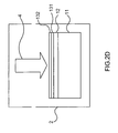
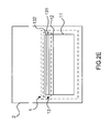
FIG.2A ,FIG.2B ,FIG.2C ,FIG.2D andFIG.2E are views showing step (a), step (b), step (c), step (d), and step(e) of the fabricating of the photosensitized electrode respectively; and -
FIG.3 is a view showing a state of use of the electrode. - The following description of the preferred embodiment is provided to understand the features and the structures of the present invention.
- Please refer to
FIG.1 , which is a structural view showing a preferred embodiment according to the present invention. As shown in the figure, the present invention is an InN_(indium nitride)/InP_(indium phosphide)/TiO2 (titanium oxide) photosensitized electrode 1, comprising asubstrate 11, a TiO2 film 12 and aphotosensitive layer 13. - The
substrate 11 is an indium tin oxide (ITO) glass, an fluorine tin oxide (FTO) glass or other transparent conductive substrate. - The TiO2
film 12 is covered on thesubstrate 11. The TiO2 film 12 has a nanoparticle structure, where a plurality of nanoparticles are evenly distributed in the TiO2 film 12, and where each nanoparticle has a diameter between 7nm (nanometer) and 50nm. The TiO2 film 12 has a thickness between 100nm and 100000nm and is made of a metal oxide having a high band-gap. - The
photosensitive layer 13 comprises an InPphotosensitive layer 131 and an InNphotosensitive layer 132. The InPphotosensitive layer 131 and the InNphotosensitive layer 132 are made through a chemical vapor deposition (CVD), a physical vapor deposition (PVD) or other epitaxial film growth method. The InPphotosensitive layer 131 is coated on the TiO2 film 12 and the InNphotosensitive layer 132 is coated on the InPphotosensitive layer 131. The InPphotosensitive layer 131 and the InNphotosensitive layer 132 both have a thickness between 1nm and 10000nm. Thus, with the above structure, a novel photosensitized electrode is obtained. - When a light penetrates through the
substrate 11 of the photosensitized electrode 1 into thephotosensitive layer 13, an electron is injected into the TiO2 film 12 from thephotosensitive layer 13 and then the electron is conducted to an outside circuit from the substrate, where thephotosensitive layer 13 absorbs an optical wavelength between 390nm and 600nm and an optical bandwidth between 390nm and 800nm. - Please refer to
FIG.2 andFIG.2A untilFIG.2E , which are a flow view showing the fabricating of the photosensitized electrode and views showing step (a) until step (e) of the fabricating of the photosensitized electrode. As shown in the figures, the fabricating of the photosensitized electrode according to the present invention comprises the following steps: - Step (a): A
substrate 11 coated with a TiO2 film 12 is placed into a reaction chamber 2, where the TiO2 film 12 is coated on thesubstrate 11 through a CVD or a PCD. - Step (b): An InP solution having nanoparticles is pasted on the TiO2 film 12 to form an InP
photosensitive layer 131, where the InP solution has nanoparticles and can be replaced with a compound containing phosphorus and a compound containing indium. - Step (c): A hydrazoic acid (HN3) 31 and a
compound containing indium 32 is introduced into the reaction chamber 2, where the ratio of HN3 31 to thecompound containing indium 32 is between 1 and 10. Thecompound containing indium 32 is a trimethylindium, a triethylindium, an indium-containing metallo-organic precursor or a combination of indium-containing metallo-organic precursors. The present invention uses the HN3 31 and thecompound containing indium 32 as precursors; and the HN3 31 can be replaced with a compound containing nitrogen. - Step (d): The substrate 11is then illuminated with an ultraviolet (UV) light, where the UV light is obtained from a continuous UV lamp, an excimer laser, a semiconductor laser, a gas laser, a solid-state laser, a liquid laser, a chemical laser or a free-electron laser, and where the TiO2 film 12 bears a temperature between 600°C (Celsius degree) and 900°C.
- Step (e): An InN
photosensitive layer 132 is obtained on the InPphotosensitive layer 131 so that the InPphotosensitive layer 131 and the InNphotosensitive layer 132 are obtained to form aphotosensitive layer 13. Thus, aphotosensitized electrode 13 is obtained, where the total process time is between 1hr and 8hrs. - Please refer to
FIG.3 , which is a view showing a state of use of the electrode. As shown in the figure, the photosensitized electrode 1 according to the present invention is assembled with aplatinum counter electrode 51 to form a solar cell device filled with anelectrolyte 52 inside. The present invention can be applied to a solar cell device, a photovoltaic device, a hydrogen generation devices and an optoelectronic device. - To sum up, the present invention is an InN/InP/TiO2 photosensitized electrode, where a lifetime issue of the dye for a Dye-Sensitized Solar Cell (DSSC) is solved; optical absorption efficiency is enhanced; a production procedure is simplified; and a production cost is reduced.
- The preferred embodiment herein disclosed is not intended to unnecessarily limit the scope of the invention. Therefore, simple modifications or variations belonging to the scope of the claims are all within the scope of the present invention.
Claims (16)
- An InN_(indium nitride)/InP_(indium phosphide)/TiO2 (titanium oxide) photosensitized electrode, comprising:a substrate (11);a TiO2 film (12) said TiO2 film covering on said substrate (11); anda photosensitive layer (13), said photosensitive layer comprising an InP photosensitive layer (131) and an InN photosensitive layer(132), said InP photosensitive layer (131) coating on said TiO2 film (12), said InN photosensitive layer (132) coating on said InP photosensitive layer (131).
- The photosensitized electrode according to claim 1, wherein said substrate (11) is a transparent conductive substrate selected from a group consisting of an indium tin oxide (ITO) glass and a fluorine tin oxide (FTO) glass.
- The photosensitized electrode according to claim 1 or 2, wherein said TiO2 film (12) has a nanoparticle structure.
- The photosensitized electrode according to claim 3, wherein said nanoparticle structure comprises a plurality of nanoparticles wherein each nanoparticle has a diameter between 7nm (nanometer) and 50nm.
- The photosensitized electrode according to one of claims 1 to 4, wherein said TiO2 film (12) has a thickness between 100nm and 100000nm.
- The photosensitized electrode according to one of claims 1 to 5, wherein said InP photosensitive layer (131) has a thickness between 1nm and 10000nm.
- The photosensitized electrode according to one of claims 1 to 6, wherein said InN photosensitive layer (132) has a thickness between 1nm and 10000nm.
- The photosensitized electrode according to one of claims 1 to 7, wherein said photosensitive layer (13) comprising said InP photosensitive layer (131) and said InN photosensitive layer (132) absorbs light having a wavelength between 390nm and 600nm.
- The photosensitized electrode according to one of claims 1 to 8, wherein said photosensitive layer (13) comprising said InP photosensitive layer (131) and said InN photosensitive layer (132) absorbs light having an optical bandwidth between 390nm and 800nm.
- A method of fabricating the photosensitized electrode of claim 1, said method comprising steps of:a. placing a substrate (11) in a reaction chamber, said substrate coated with a TiO2 film (12);b. pasting said TiO2 film (12) with an InP solution having nanoparticles to obtain an InP photosensitive layer(131);c. introducing hydrazoic acid (HN3) and a compound containing indium into said reaction chamber;d. illuminating said InP photosensitive layer (131) with an ultraviolet (UV) light; ande. obtaining an InN photosensitive layer (132) coated on said InP photosensitive layer (131).
- The method according to claim 10, wherein said compound containing indium is selected from a group consisting of a trimethylindium, a triethylindium, a indium-containing metallo-organic precursor and a combination of indium-containing metallo-organic precursors.
- The method according to claim 10 or 11, wherein said hydrazoic acid is a compound containing indium.
- The method according to one of claims 10 to 12, wherein a ratio of said HN3 to said compound containing indium is between 1 and 10.
- The method according to one of claims 10 to 13, wherein said Ti02 film (12) bears a temperature between 600°C (Celsius degrees) and 900°C.
- The method according to one of claims 10 to 14, wherein a period of time for processing all steps of said step (a) until step (e) is between 1hr (hour) and 8hrs.
- The method according to one of claims 10 to 15, wherein said UV light is obtained from a light source selected from a group consisting of a continuous UV lamp, an excimer laser, a semiconductor laser, a gas laser, a solid-state laser, a liquid laser, a chemical laser and a free-electron laser.
Priority Applications (3)
| Application Number | Priority Date | Filing Date | Title |
|---|---|---|---|
| EP06118588A EP1887592B1 (en) | 2006-08-08 | 2006-08-08 | InN/InP/TiO2 photosensitized electrode |
| AT06118588T ATE420448T1 (en) | 2006-08-08 | 2006-08-08 | INN/INP/TIO2 PHOTOSENSITIZED ELECTRODE |
| DE602006004730T DE602006004730D1 (en) | 2006-08-08 | 2006-08-08 | InN / InP / TiO2 photosensitized electrode |
Applications Claiming Priority (1)
| Application Number | Priority Date | Filing Date | Title |
|---|---|---|---|
| EP06118588A EP1887592B1 (en) | 2006-08-08 | 2006-08-08 | InN/InP/TiO2 photosensitized electrode |
Publications (2)
| Publication Number | Publication Date |
|---|---|
| EP1887592A1 EP1887592A1 (en) | 2008-02-13 |
| EP1887592B1 true EP1887592B1 (en) | 2009-01-07 |
Family
ID=37757114
Family Applications (1)
| Application Number | Title | Priority Date | Filing Date |
|---|---|---|---|
| EP06118588A Not-in-force EP1887592B1 (en) | 2006-08-08 | 2006-08-08 | InN/InP/TiO2 photosensitized electrode |
Country Status (3)
| Country | Link |
|---|---|
| EP (1) | EP1887592B1 (en) |
| AT (1) | ATE420448T1 (en) |
| DE (1) | DE602006004730D1 (en) |
Family Cites Families (1)
| Publication number | Priority date | Publication date | Assignee | Title |
|---|---|---|---|---|
| KR101117689B1 (en) * | 2005-01-22 | 2012-02-29 | 삼성전자주식회사 | Photoreceptive layer comprising various dye and solar cells using the same |
-
2006
- 2006-08-08 EP EP06118588A patent/EP1887592B1/en not_active Not-in-force
- 2006-08-08 AT AT06118588T patent/ATE420448T1/en not_active IP Right Cessation
- 2006-08-08 DE DE602006004730T patent/DE602006004730D1/en active Active
Also Published As
| Publication number | Publication date |
|---|---|
| ATE420448T1 (en) | 2009-01-15 |
| DE602006004730D1 (en) | 2009-02-26 |
| EP1887592A1 (en) | 2008-02-13 |
Similar Documents
| Publication | Publication Date | Title |
|---|---|---|
| Hu et al. | Atomic layer deposition of TiO2 for a high-efficiency hole-blocking layer in hole-conductor-free perovskite solar cells processed in ambient air | |
| Li et al. | In situ interface engineering for highly efficient electron-transport-layer-free perovskite solar cells | |
| Dkhili et al. | Attributes of high-performance electron transport layers for perovskite solar cells on flexible PET versus on glass | |
| Yang et al. | Effective carrier‐concentration tuning of SnO2 quantum dot electron‐selective layers for high‐performance planar perovskite solar cells | |
| Jiao et al. | Nitrogen-doped mesoporous carbons as counter electrodes in quantum dot sensitized solar cells with a conversion efficiency exceeding 12% | |
| Li et al. | Efficient perovskite solar cells depending on TiO2 nanorod arrays | |
| Ding et al. | Facile and scalable fabrication of highly efficient lead iodide perovskite thin-film solar cells in air using gas pump method | |
| Roh et al. | High efficiency solid‐state dye‐sensitized solar cells assembled with hierarchical anatase pine tree‐like TiO2 nanotubes | |
| Koo et al. | Improvement of transparent conducting performance on oxygen-activated fluorine-doped tin oxide electrodes formed by horizontal ultrasonic spray pyrolysis deposition | |
| Passoni et al. | Hyperbranched quasi-1D nanostructures for solid-state dye-sensitized solar cells | |
| Wu et al. | Thin films of dendritic anatase titania nanowires enable effective hole‐blocking and efficient light‐harvesting for high‐performance mesoscopic perovskite solar cells | |
| Chandiran et al. | Low-temperature crystalline titanium dioxide by atomic layer deposition for dye-sensitized solar cells | |
| Wang et al. | Solution-processed Sb2Se3 on TiO2 thin films toward oxidation-and moisture-resistant, self-powered photodetectors | |
| Li et al. | Grain size and interface modification via cesium carbonate post-treatment for efficient SnO2-based planar perovskite solar cells | |
| Kanda et al. | Interface optoelectronics engineering for mechanically stacked tandem solar cells based on perovskite and silicon | |
| Heo et al. | Sb2S3-sensitized photoelectrochemical cells: open circuit voltage enhancement through the introduction of poly-3-hexylthiophene interlayer | |
| US20090114278A1 (en) | Dye-sensitized solar cell and fabrication method thereof | |
| Alberti et al. | Nanostructured TiO2 grown by low-temperature reactive sputtering for planar perovskite solar cells | |
| Shivarudraiah et al. | Optically clear films of formamidinium lead bromide perovskite for wide-band-gap, solution-processed, semitransparent solar cells | |
| Lalpour et al. | Self-healing perovskite solar cells based on copolymer-templated TiO2 electron transport layer | |
| Sun et al. | Highly efficient large-area flexible perovskite solar cells containing tin oxide vertical nanopillars without oxygen vacancies | |
| Zia et al. | MAPbCl3 light absorber for highest voltage perovskite solar cells | |
| Liu et al. | Area-scalable Zn2SnO4 electron transport layer for highly efficient and stable perovskite solar modules | |
| Parvazian et al. | Photovoltaic performance improvement in vacuum-assisted meniscus printed triple-cation mixed-halide perovskite films by surfactant engineering | |
| Ma et al. | Facile sol–gel-derived craterlike dual-functioning TiO2 electron transport layer for high-efficiency perovskite solar cells |
Legal Events
| Date | Code | Title | Description |
|---|---|---|---|
| PUAI | Public reference made under article 153(3) epc to a published international application that has entered the european phase |
Free format text: ORIGINAL CODE: 0009012 |
|
| 17P | Request for examination filed |
Effective date: 20060905 |
|
| AK | Designated contracting states |
Kind code of ref document: A1 Designated state(s): AT BE BG CH CY CZ DE DK EE ES FI FR GB GR HU IE IS IT LI LT LU LV MC NL PL PT RO SE SI SK TR |
|
| AX | Request for extension of the european patent |
Extension state: AL BA HR MK YU |
|
| GRAP | Despatch of communication of intention to grant a patent |
Free format text: ORIGINAL CODE: EPIDOSNIGR1 |
|
| AKX | Designation fees paid |
Designated state(s): AT BE BG CH CY CZ DE DK EE ES FI FR GB GR HU IE IS IT LI LT LU LV MC NL PL PT RO SE SI SK TR |
|
| GRAS | Grant fee paid |
Free format text: ORIGINAL CODE: EPIDOSNIGR3 |
|
| GRAA | (expected) grant |
Free format text: ORIGINAL CODE: 0009210 |
|
| AK | Designated contracting states |
Kind code of ref document: B1 Designated state(s): AT BE BG CH CY CZ DE DK EE ES FI FR GB GR HU IE IS IT LI LT LU LV MC NL PL PT RO SE SI SK TR |
|
| REG | Reference to a national code |
Ref country code: GB Ref legal event code: FG4D |
|
| REG | Reference to a national code |
Ref country code: CH Ref legal event code: EP |
|
| REG | Reference to a national code |
Ref country code: IE Ref legal event code: FG4D |
|
| REF | Corresponds to: |
Ref document number: 602006004730 Country of ref document: DE Date of ref document: 20090226 Kind code of ref document: P |
|
| PG25 | Lapsed in a contracting state [announced via postgrant information from national office to epo] |
Ref country code: SI Free format text: LAPSE BECAUSE OF FAILURE TO SUBMIT A TRANSLATION OF THE DESCRIPTION OR TO PAY THE FEE WITHIN THE PRESCRIBED TIME-LIMIT Effective date: 20090107 Ref country code: NL Free format text: LAPSE BECAUSE OF FAILURE TO SUBMIT A TRANSLATION OF THE DESCRIPTION OR TO PAY THE FEE WITHIN THE PRESCRIBED TIME-LIMIT Effective date: 20090107 |
|
| NLV1 | Nl: lapsed or annulled due to failure to fulfill the requirements of art. 29p and 29m of the patents act | ||
| PG25 | Lapsed in a contracting state [announced via postgrant information from national office to epo] |
Ref country code: FI Free format text: LAPSE BECAUSE OF FAILURE TO SUBMIT A TRANSLATION OF THE DESCRIPTION OR TO PAY THE FEE WITHIN THE PRESCRIBED TIME-LIMIT Effective date: 20090107 Ref country code: ES Free format text: LAPSE BECAUSE OF FAILURE TO SUBMIT A TRANSLATION OF THE DESCRIPTION OR TO PAY THE FEE WITHIN THE PRESCRIBED TIME-LIMIT Effective date: 20090418 Ref country code: LT Free format text: LAPSE BECAUSE OF FAILURE TO SUBMIT A TRANSLATION OF THE DESCRIPTION OR TO PAY THE FEE WITHIN THE PRESCRIBED TIME-LIMIT Effective date: 20090107 |
|
| PG25 | Lapsed in a contracting state [announced via postgrant information from national office to epo] |
Ref country code: AT Free format text: LAPSE BECAUSE OF FAILURE TO SUBMIT A TRANSLATION OF THE DESCRIPTION OR TO PAY THE FEE WITHIN THE PRESCRIBED TIME-LIMIT Effective date: 20090107 Ref country code: PL Free format text: LAPSE BECAUSE OF FAILURE TO SUBMIT A TRANSLATION OF THE DESCRIPTION OR TO PAY THE FEE WITHIN THE PRESCRIBED TIME-LIMIT Effective date: 20090107 Ref country code: SE Free format text: LAPSE BECAUSE OF FAILURE TO SUBMIT A TRANSLATION OF THE DESCRIPTION OR TO PAY THE FEE WITHIN THE PRESCRIBED TIME-LIMIT Effective date: 20090407 Ref country code: PT Free format text: LAPSE BECAUSE OF FAILURE TO SUBMIT A TRANSLATION OF THE DESCRIPTION OR TO PAY THE FEE WITHIN THE PRESCRIBED TIME-LIMIT Effective date: 20090608 Ref country code: IS Free format text: LAPSE BECAUSE OF FAILURE TO SUBMIT A TRANSLATION OF THE DESCRIPTION OR TO PAY THE FEE WITHIN THE PRESCRIBED TIME-LIMIT Effective date: 20090507 Ref country code: LV Free format text: LAPSE BECAUSE OF FAILURE TO SUBMIT A TRANSLATION OF THE DESCRIPTION OR TO PAY THE FEE WITHIN THE PRESCRIBED TIME-LIMIT Effective date: 20090107 |
|
| PG25 | Lapsed in a contracting state [announced via postgrant information from national office to epo] |
Ref country code: BE Free format text: LAPSE BECAUSE OF FAILURE TO SUBMIT A TRANSLATION OF THE DESCRIPTION OR TO PAY THE FEE WITHIN THE PRESCRIBED TIME-LIMIT Effective date: 20090107 |
|
| PG25 | Lapsed in a contracting state [announced via postgrant information from national office to epo] |
Ref country code: EE Free format text: LAPSE BECAUSE OF FAILURE TO SUBMIT A TRANSLATION OF THE DESCRIPTION OR TO PAY THE FEE WITHIN THE PRESCRIBED TIME-LIMIT Effective date: 20090107 Ref country code: DK Free format text: LAPSE BECAUSE OF FAILURE TO SUBMIT A TRANSLATION OF THE DESCRIPTION OR TO PAY THE FEE WITHIN THE PRESCRIBED TIME-LIMIT Effective date: 20090107 Ref country code: CZ Free format text: LAPSE BECAUSE OF FAILURE TO SUBMIT A TRANSLATION OF THE DESCRIPTION OR TO PAY THE FEE WITHIN THE PRESCRIBED TIME-LIMIT Effective date: 20090107 |
|
| PLBE | No opposition filed within time limit |
Free format text: ORIGINAL CODE: 0009261 |
|
| STAA | Information on the status of an ep patent application or granted ep patent |
Free format text: STATUS: NO OPPOSITION FILED WITHIN TIME LIMIT |
|
| PG25 | Lapsed in a contracting state [announced via postgrant information from national office to epo] |
Ref country code: RO Free format text: LAPSE BECAUSE OF FAILURE TO SUBMIT A TRANSLATION OF THE DESCRIPTION OR TO PAY THE FEE WITHIN THE PRESCRIBED TIME-LIMIT Effective date: 20090107 Ref country code: SK Free format text: LAPSE BECAUSE OF FAILURE TO SUBMIT A TRANSLATION OF THE DESCRIPTION OR TO PAY THE FEE WITHIN THE PRESCRIBED TIME-LIMIT Effective date: 20090107 |
|
| 26N | No opposition filed |
Effective date: 20091008 |
|
| PG25 | Lapsed in a contracting state [announced via postgrant information from national office to epo] |
Ref country code: BG Free format text: LAPSE BECAUSE OF FAILURE TO SUBMIT A TRANSLATION OF THE DESCRIPTION OR TO PAY THE FEE WITHIN THE PRESCRIBED TIME-LIMIT Effective date: 20090407 |
|
| PG25 | Lapsed in a contracting state [announced via postgrant information from national office to epo] |
Ref country code: MC Free format text: LAPSE BECAUSE OF NON-PAYMENT OF DUE FEES Effective date: 20090831 |
|
| REG | Reference to a national code |
Ref country code: FR Ref legal event code: ST Effective date: 20100430 |
|
| PG25 | Lapsed in a contracting state [announced via postgrant information from national office to epo] |
Ref country code: IE Free format text: LAPSE BECAUSE OF NON-PAYMENT OF DUE FEES Effective date: 20090808 Ref country code: FR Free format text: LAPSE BECAUSE OF NON-PAYMENT OF DUE FEES Effective date: 20090831 |
|
| PG25 | Lapsed in a contracting state [announced via postgrant information from national office to epo] |
Ref country code: GR Free format text: LAPSE BECAUSE OF FAILURE TO SUBMIT A TRANSLATION OF THE DESCRIPTION OR TO PAY THE FEE WITHIN THE PRESCRIBED TIME-LIMIT Effective date: 20090408 |
|
| PGFP | Annual fee paid to national office [announced via postgrant information from national office to epo] |
Ref country code: DE Payment date: 20100720 Year of fee payment: 5 |
|
| PG25 | Lapsed in a contracting state [announced via postgrant information from national office to epo] |
Ref country code: IT Free format text: LAPSE BECAUSE OF FAILURE TO SUBMIT A TRANSLATION OF THE DESCRIPTION OR TO PAY THE FEE WITHIN THE PRESCRIBED TIME-LIMIT Effective date: 20090107 |
|
| REG | Reference to a national code |
Ref country code: CH Ref legal event code: PL |
|
| GBPC | Gb: european patent ceased through non-payment of renewal fee |
Effective date: 20100808 |
|
| PG25 | Lapsed in a contracting state [announced via postgrant information from national office to epo] |
Ref country code: LI Free format text: LAPSE BECAUSE OF NON-PAYMENT OF DUE FEES Effective date: 20100831 Ref country code: CH Free format text: LAPSE BECAUSE OF NON-PAYMENT OF DUE FEES Effective date: 20100831 Ref country code: LU Free format text: LAPSE BECAUSE OF NON-PAYMENT OF DUE FEES Effective date: 20090808 |
|
| PG25 | Lapsed in a contracting state [announced via postgrant information from national office to epo] |
Ref country code: HU Free format text: LAPSE BECAUSE OF FAILURE TO SUBMIT A TRANSLATION OF THE DESCRIPTION OR TO PAY THE FEE WITHIN THE PRESCRIBED TIME-LIMIT Effective date: 20090708 |
|
| PG25 | Lapsed in a contracting state [announced via postgrant information from national office to epo] |
Ref country code: TR Free format text: LAPSE BECAUSE OF FAILURE TO SUBMIT A TRANSLATION OF THE DESCRIPTION OR TO PAY THE FEE WITHIN THE PRESCRIBED TIME-LIMIT Effective date: 20090107 Ref country code: GB Free format text: LAPSE BECAUSE OF NON-PAYMENT OF DUE FEES Effective date: 20100808 |
|
| PG25 | Lapsed in a contracting state [announced via postgrant information from national office to epo] |
Ref country code: CY Free format text: LAPSE BECAUSE OF FAILURE TO SUBMIT A TRANSLATION OF THE DESCRIPTION OR TO PAY THE FEE WITHIN THE PRESCRIBED TIME-LIMIT Effective date: 20090107 |
|
| REG | Reference to a national code |
Ref country code: DE Ref legal event code: R119 Ref document number: 602006004730 Country of ref document: DE Effective date: 20120301 |
|
| PG25 | Lapsed in a contracting state [announced via postgrant information from national office to epo] |
Ref country code: DE Free format text: LAPSE BECAUSE OF NON-PAYMENT OF DUE FEES Effective date: 20120301 |