EP1887411A2 - Manufacturing method for variable shape mirror - Google Patents
Manufacturing method for variable shape mirror Download PDFInfo
- Publication number
- EP1887411A2 EP1887411A2 EP07015392A EP07015392A EP1887411A2 EP 1887411 A2 EP1887411 A2 EP 1887411A2 EP 07015392 A EP07015392 A EP 07015392A EP 07015392 A EP07015392 A EP 07015392A EP 1887411 A2 EP1887411 A2 EP 1887411A2
- Authority
- EP
- European Patent Office
- Prior art keywords
- substrate
- mirror
- support
- variable shape
- mirror substrate
- Prior art date
- Legal status (The legal status is an assumption and is not a legal conclusion. Google has not performed a legal analysis and makes no representation as to the accuracy of the status listed.)
- Granted
Links
Images


Classifications
-
- G—PHYSICS
- G02—OPTICS
- G02B—OPTICAL ELEMENTS, SYSTEMS OR APPARATUS
- G02B26/00—Optical devices or arrangements for the control of light using movable or deformable optical elements
- G02B26/08—Optical devices or arrangements for the control of light using movable or deformable optical elements for controlling the direction of light
- G02B26/0816—Optical devices or arrangements for the control of light using movable or deformable optical elements for controlling the direction of light by means of one or more reflecting elements
- G02B26/0833—Optical devices or arrangements for the control of light using movable or deformable optical elements for controlling the direction of light by means of one or more reflecting elements the reflecting element being a micromechanical device, e.g. a MEMS mirror, DMD
- G02B26/0858—Optical devices or arrangements for the control of light using movable or deformable optical elements for controlling the direction of light by means of one or more reflecting elements the reflecting element being a micromechanical device, e.g. a MEMS mirror, DMD the reflecting means being moved or deformed by piezoelectric means
-
- G—PHYSICS
- G02—OPTICS
- G02B—OPTICAL ELEMENTS, SYSTEMS OR APPARATUS
- G02B26/00—Optical devices or arrangements for the control of light using movable or deformable optical elements
- G02B26/06—Optical devices or arrangements for the control of light using movable or deformable optical elements for controlling the phase of light
Definitions
- the present invention relates to a manufacturing method for a variable shape mirror that is mounted on an optical pickup device.
- a compact discs (CD) and a digital versatile disc (DVD) are available in the market as an optical recording medium for recording information such as images and sounds.
- a next-generation DVD are being commercialized, which uses a laser beam of violet color having a short wavelength for realizing higher density recording.
- an optical disc apparatus is necessary as a driving apparatus. The optical disc apparatus drives the optical disc to rotate and leads the laser beam onto a recording surface of the optical disc, so that information is recorded or erased and that information is reproduced based on reflection light from the recording surface.
- the optical disc apparatus is equipped with an optical pickup device as a set of units for emitting the laser beam, leading the laser beam onto the recording surface of the optical disc to form a beam spot, and receiving reflection light from the recording surface of the optical disc.
- optical pickup devices particularly next-generation DVDs are adapted to a high numerical aperture (NA) in accordance with a standard to conform.
- NA numerical aperture
- the optical axis of the laser beam may be inclined slightly with respect to the recording surface resulting from warpage or the like of the optical disc.
- the optical path of the laser beam is bent so that coma aberration is generated, which makes it difficult to condense the laser beam into an appropriate spot diameter.
- recording and reproducing quality is deteriorated.
- There are other factors of deterioration of recording and reproducing quality which includes positioning accuracy of an optical system such as an optical lens or a beam splitter that is an element of the optical pickup device, which causes astigmatic aberration.
- variable shape mirror that can correct wave aberration such as the spherical aberration.
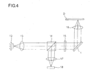
- the optical pickup device adopting a variable shape mirror 1 in the optical system is made up of a semiconductor laser 12, a collimator lens 13, a beam splitter 14, the variable shape mirror 1, a quarter wave length plate 15, an objective lens 16, a condensing lens 17, a photo detector 18 and the like.
- a laser beam emitted from the semiconductor laser 12 is made into parallel rays by the collimator lens 13, passes through the beam splitter 14, is reflected by the variable shape mirror 1 after its polarized state is changed by the quarter wave length plate 15, and is condensed by the objective lens 16 so as to reach the recording surface of the optical disc D. Further, the laser beam reflected by the recording surface of the optical disc D passes through the objective lens 16, is reflected by the variable shape mirror 1, passes through the quarter wave length plate 15, then is reflected by the beam splitter 14 this time, and is condensed by the condensing lens 17 so as to reach the photo detector 18 at last.
- the variable shape mirror 1 has a function of a so-called rise up mirror that reflects the laser beam toward the optical disc D and reflects the reflection light from the optical disc D in parallel with the optical disc D. It also has a function of changing its reflection plane if necessary for fine adjustment of a reflection angle of the laser beam, so that wave aberration is corrected. In this case, based on a signal obtained by the photo detector 18, if it is necessary to correct wave aberration, a control portion that is provided to the optical pickup device sends a signal to the variable shape mirror 1 so that a shape of the reflection plane is changed for correcting the aberration.
- variable shape mirror 1 there is a type that utilizes characteristics of a piezoelectric element made of a piezoelectric material (see JP-A-2004-109769 and JP-A-2004-226457 , for example).
- This variable shape mirror 1 is generally made up of a support substrate, a mirror substrate that is supported by a support pillar and is opposed to the support substrate, and a piezoelectric element sandwiched between the support substrate and the mirror substrate.
- the outer surface of the mirror substrate is provided with a reflection film to be a reflection plane for the laser beam.
- variable shape mirror Under the present circumstances, a manufacturing method for such a variable shape mirror that is suitable for mass production is not established yet.
- the support substrate and the mirror substrate that constitute each variable shape mirror are cut from the wafers, and the support pillar and the piezoelectric element are sandwiched between the support substrate and the mirror substrate. Then, the both wafers and the support pillar, as well as the both wafers and the piezoelectric element are bonded to each other, individually. Then, the reflection film is formed on the outer surface of the mirror substrate.
- the variable shape mirror can be obtained at least.
- variable shape mirrors which is suitable for mass production.
- each of the variable shape mirrors including: a support substrate; a mirror substrate that is opposed to the support substrate and is supported by support pillars and has a reflection film on the surface; and piezoelectric elements that are sandwiched between the support substrate and the mirror substrate and are expanded or contracted when an electric field is applied so as to deform the mirror substrate and the reflection film
- the manufacturing method is characterized by including: a bonding step for sandwiching the support pillars and the piezoelectric elements between the support substrate and the mirror substrate, and bonding at least the support substrate and the support pillar to each other, the support substrate and the piezoelectric element to each other, and the mirror substrate and the support pillars to each other, respectively; an elastic film forming step for forming a flat elastic film on the outer surface of the mirror substrate; and a reflection film forming step for forming the reflection film on the elastic film.
- a reflection film is formed on the outer surface of the flat elastic film that is formed on the outer surface of the mirror substrate. Therefore, the reflection plane of the reflection film also becomes flat, so that a variable shape mirror having good quality can be obtained securely.
- the elastic film is made of a resin.
- thin metal layers are disposed at bonding portions between the support substrate and the support pillars, and the bonding portions between the support substrate and the piezoelectric elements, and they are pressed to each other while they are heated so as to be bonded.
- thin metal layers are disposed at bonding portions between the mirror substrate and the support pillars, and the bonding portions between the mirror substrate and the piezoelectric elements, and they are pressed to each other while they are heated so as to be bonded.
- variable shape mirrors of the present invention According to the manufacturing method for variable shape mirrors of the present invention, a variable shape mirror having good quality can be obtained securely, and the method is suitable for mass production.
- Figs. 1A and 1B are cross sectional views of a variable shape mirror that is manufactured by a manufacturing method according to an embodiment of the present invention.
- Fig. 1A shows an undriven state
- Fig. 1B shows a driven state.
- Fig. 2 is a an exploded perspective view of the variable shape mirror to show its general structure
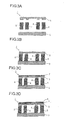
- Fig. 3A-3D are cross sectional views of the variable shape mirror to show a procedure of the manufacturing method for variable shape mirrors according to an embodiment of the present invention.
- variable shape mirror 1 As shown in Figs. 1A and 2, the variable shape mirror 1 in the present embodiment includes a support substrate 2 having a substantially square shape, a mirror substrate 3 that has a substantially square shape of a little smaller size than the support substrate 2 and is opposed to the support substrate 2, a plurality of piezoelectric elements 4 and a plurality of support pillars 5 that are sandwiched between the support substrate 2 and the mirror substrate 3 at predetermined positions.
- the variable shape mirror 1 of this embodiment includes the support pillars 5 disposed at four corners and at substantially centers of four sides of the mirror substrate 3 as shown in Fig. 2, and the piezoelectric elements 4 are disposed inside the support pillars 5 disposed at four sides with a predetermined space. In other words, the piezoelectric elements 4 and the support pillars 5 are disposed in this order outward from the center of the mirror substrate 3 in the cross direction.
- the support substrate 2 is a base for supporting individual components.
- glass can be used. However, other materials as long as having insulation characteristics, such as ceramics, can also be used.
- This support substrate 2 is provided with a thin film portion made of silicon (Si) that is formed on the surface facing the mirror substrate 3 (i.e., the inner surface) at the positions where the piezoelectric elements 4 and the support pillars 5 are disposed (hatched portions in Fig. 2).
- a wiring pattern (not shown) made of the same Si is lead out to a vicinity to the edge of the support substrate 2 from the Si thin film portion of the position where the piezoelectric element 4 are disposed.
- the Si thin film portions and the Si wiring patterns are formed by photo lithography or the like.
- the mirror substrate 3 is a plate that is capable of being deformed in an elastic manner.
- Si can be used.
- glass or the like, for example, can also be used as long as it can be deformed in an elastic manner.
- This mirror substrate 3 is provided with an elastic film 7 that has a function as a reflection plane that is formed on the substantially entire surface (outer surface) opposite to the surface (inner surface) facing the support substrate 2.
- a resin of an epoxy system or a polyimide system or the like can be used. However, the material is not limited as long as it can be deformed in an elastic manner.
- This elastic film 7 is provided with a reflection film 6 that has a function as a reflection plane that is formed on the substantially entire surface.
- the reflection film 6 is a metal film made of aluminum (Al) or the like, which is formed by vapor deposition or sputtering or the like.
- the piezoelectric element 4 is formed in a rectangular solid shape made of a piezoelectric material that is expanded or contracted when an electric field is applied.
- a piezoelectric material that is expanded or contracted when an electric field is applied.
- PZT Pb(Zr,Ti)O3, lead zirconate titanate
- it can be other piezoelectric ceramics except the PZT or piezoelectric polymer such as a polyvinylidene fluoride or the like.
- the shape of the piezoelectric element 4 can be a cylindrical shape or a rectangular column shape.
- Each of the piezoelectric elements 4 is bonded onto the Si thin film portion formed on the inner surface of the support substrate 2 via a metal thin layer portion (not shown).
- a metal thin layer portion As a material of the thin metal layer portion, Au (gold) can be used, and the thin metal layer portion is formed on the Si thin film portion on the inner surface of the support substrate 2 by vapor deposition or sputtering or the like.
- the thin metal layer portion can be made of not only Au but also Pt (platinum) or the like.
- the support substrate 2 and each of the piezoelectric elements 4 are pressed to each other while they are heated, so that metal (Au) atoms of the thin metal layer portion between them are diffused into the Si thin film portion on the inner surface of the support substrate 2 and into the piezoelectric element 4 (PZT).
- PZT piezoelectric element 4
- the mirror substrate 3 is bonded onto each of the piezoelectric elements 4 via a thin metal layer portion (not shown) by the diffused junction.
- the thin metal layer portion is formed on the inner surface of the mirror substrate 3 by vapor deposition or sputtering or the like.
- the Si thin film portion on the inner surface of the support substrate 2 is connected electrically to each of the piezoelectric elements 4 via the thin metal layer portion so as to be a separated electrode for applying an electric-field to each of the piezoelectric elements 4.
- the mirror substrate 3 made of Si is connected electrically to each of the piezoelectric elements 4 via the thin metal layer portion so as to be a common electrode for applying an electric field to each of the piezoelectric elements 4.
- the thin metal film portion is used as a type of adhesive for bonding the support substrate 2 and the piezoelectric element 4 to each other, and for bonding the mirror substrate 3 and the piezoelectric element 4 to each other by the diffused junction in the present embodiment, it is possible to use a conductive adhesive for bonding them.
- a nonconductive adhesive of epoxy system or the like for bonding them, but in this case, it is necessary to make electric connection between the Si wiring pattern from the Si thin film portion on the inner surface of the support substrate 2 and the piezoelectric element 4, and between the mirror substrate 3 made of Si and the piezoelectric element 4 by additional wire bonding or the like.
- the mirror substrate 3 and the piezoelectric element 4 are bonded to each other in the present embodiment, it is possible to use a laminated piezoelectric element with electrodes drawn out from both sides can be used as the piezoelectric element 4, for example.
- a laminated piezoelectric element with electrodes drawn out from both sides can be used as the piezoelectric element 4, for example.
- the Si thin film portion on the inner surface of the support substrate 2 is divided into two parts so that each of the Si thin film portions is connected to each electrode of the laminated piezoelectric element, an electric field can be applied to each of the piezoelectric elements 4. Therefore, it is sufficient to make a simple contact state between the mirror substrate 3 and the piezoelectric element 4 without bonding them to each other.
- the support pillar 5 supports the mirror substrate 3.
- the support pillar 5 in the present embodiment is made of the same material as the piezoelectric element 4 and is bonded to the support substrate 2 and the mirror substrate 3 in the same manner as the above-mentioned piezoelectric element 4.
- the support pillar 5 is formed separately from the support substrate 2 in the present embodiment, it is possible to form it integrally with the support substrate 2.
- variable shape mirror 1 As to the variable shape mirror 1 having the structure described above, the reflection plane of the mirror substrate 3 of the reflection film 6 is flat as shown in Fig. 1A, in the undriven state, i.e., the state where a voltage is not applied to each of the piezoelectric elements 4.
- a predetermined voltage is applied to each of the piezoelectric elements 4 so that an electric field is applied for driving
- each of the piezoelectric elements 4 is expanded between the support substrate 2 and the mirror substrate 3 as shown in Fig. 1B.
- the mirror substrate 3 is pressed upward so as to be deformed elastically in a convex shape, and the reflection plane of the reflection film 6 is deformed following the deformation of the mirror substrate 3. Therefore, use of this variable shape mirror 1 in the optical system of the optical pickup device enables correction of wave aberration in the laser beam.
- the support substrate 2, the mirror substrate 3, the piezoelectric elements 4, and the support pillars 5 that are individual elements of the variable shape mirror 1 are prepared.
- the support substrate 2 and the mirror substrate 3 are cut out from each wafer and are prepared.
- the Si thin film portion, the Si wiring pattern and the thin metal layer portion that are described above as the structure of the variable shape mirror 1 are formed on a surface of the support substrate 2, while the thin metal layer portion is formed on a surface of the mirror substrate 3.
- the support substrate 2 and the mirror substrate 3 are arranged so that the surface of the support substrate 2 on which the Si thin film portions and the like are formed and the surface of the mirror substrate 3 on which the thin metal layer portions are formed face each other.
- the support pillars 5 and the piezoelectric elements 4 are sandwiched between the support substrate 2 and the mirror substrate 3, so as to bond the support substrate 2 and the support pillars 5, the support substrate 2 and the piezoelectric elements 4, the mirror substrate 3 and the support pillars 5, and the mirror substrate 3 and the piezoelectric elements 4 to each other, respectively.
- the support substrate 2 and the support pillars 5, the support substrate 2 and the piezoelectric elements 4, the mirror substrate 3 and the support pillars 5, and the mirror substrate 3 and the piezoelectric elements 4 are pressed to each other while they are heated, so that the support substrate 2 and the support pillars 5, the support substrate 2 and the piezoelectric elements 4, the mirror substrate 3 and the support pillars 5, and the mirror substrate 3 and the piezoelectric elements 4 are bonded securely to each other by the diffused junction.
- the mirror substrate 3 and the piezoelectric elements 4 may be just contacted with each other without bonding.
- the flat elastic film 7 is formed so as to cover the entire outer surface of the mirror substrate 3.
- resin is used as the elastic film 7, and the flat elastic film 7 having a flat outer surface is formed on the outer surface of the mirror substrate 3 as follows.
- the mirror substrate 3 is rotated at high speed and the resin is dropped on the outer surface of the mirror substrate 3 that is rotating, like a spin coat method.
- the resin is poured into a mold having a flat recess shape, and the mirror substrate 3 is placed on it from the outer surface. Then, the resin is released from the mold after the resin is cured.
- the resin is coated onto the outer surface of the mirror substrate 3, and the surface of the resin is heated up to a temperature above a glass transition point of the resin. In this state, a flat plate is pressed to the surface of the resin.
- the reflection film 6 is formed on the flat outer surface of the elastic film 7. In this way, the variable shape mirror 1 is obtained.
- variable shape mirror 1 obtained as described above has the reflection film 6 formed on the flat surface of the elastic film 7 on the outer surface of the mirror substrate 3, the surface of the reflection film 6 is also flat. Therefore, according to the manufacturing method of the present embodiment, the variable shape mirror 1 having good quality can be obtained securely. Accordingly, the manufacturing method of the present embodiment is sufficiently suitable for mass production.
- the elastic film 7 and the reflection film 6 are individual members in the present embodiment, it is possible that they share the same member. More specifically, the elastic film 7 may be made of the same metal as the reflection film 6 on the outer surface of the mirror substrate 3 so as to have a thickness to some extent, and a flat grindstone may be pressed on the entire outer surface of the elastic film 7 so as to polish the same. Then, a flat reflection plane is formed as it is without forming the additional reflection film 6.
- variable shape mirrors 1 are manufactured by using the support substrate 2 and the mirror substrate 3 in a chip level cut out from the wafer in advance in the embodiment described above, it is possible that individual variable shape mirrors 1 are assembled at the stage of the wafer, and then the wafer is divided into the individual variable shape mirrors 1.
- wafers to be the support substrate 2 and the mirror substrate 3, respectively, are prepared, and the support pillars 5 and the piezoelectric elements 4 are sandwiched between the wafers, so that the wafers and the support pillars 5, and the wafers and the piezoelectric elements 4 are bonded to each other, respectively.
- the elastic film 7 is formed on the outer surface of the wafer to be the mirror substrate 3.
- each of the wafers is cut individually by a disc-shaped dicing saw along boundaries between the areas to be the individual variable shape mirrors 1, so that it is divided into the individual variable shape mirrors 1.
- a reflection film 6 is formed on the outer surface of the mirror substrate 3 of each variable shape mirror 1.
- variable shape mirrors 1 can be obtained at the same time, so manufacturing efficiency for the variable shape mirrors 1 is improved, and the method is more suitable for mass production. Note that this method enables the thin fragile wafer as the mirror substrate 3 to be reinforced by the elastic film 7, so it is possible to decrease damages to the wafer due to chipping or breaking when the wafer is cut by the dicing saw.
- the manufacturing method of the present invention is suitable for the variable shape mirrors.
Landscapes
- Physics & Mathematics (AREA)
- General Physics & Mathematics (AREA)
- Optics & Photonics (AREA)
- Mechanical Light Control Or Optical Switches (AREA)
- Optical Elements Other Than Lenses (AREA)
- Micromachines (AREA)
- Optical Head (AREA)
- Mechanical Optical Scanning Systems (AREA)
Abstract
Description
- The present invention relates to a manufacturing method for a variable shape mirror that is mounted on an optical pickup device.
- Conventionally, a compact discs (CD) and a digital versatile disc (DVD) are available in the market as an optical recording medium for recording information such as images and sounds. Further, in recent years, a next-generation DVD are being commercialized, which uses a laser beam of violet color having a short wavelength for realizing higher density recording. In order to use such an optical disc, an optical disc apparatus is necessary as a driving apparatus. The optical disc apparatus drives the optical disc to rotate and leads the laser beam onto a recording surface of the optical disc, so that information is recorded or erased and that information is reproduced based on reflection light from the recording surface. Further, in order to realize such a function, the optical disc apparatus is equipped with an optical pickup device as a set of units for emitting the laser beam, leading the laser beam onto the recording surface of the optical disc to form a beam spot, and receiving reflection light from the recording surface of the optical disc.
- Here, optical pickup devices, particularly next-generation DVDs are adapted to a high numerical aperture (NA) in accordance with a standard to conform. In this case, influence of the spherical aberration that is generated when a thickness of the optical disc varies slightly becomes conspicuous so that a minute beam spot may not be obtained. Therefore, jitter of a reproduced signal is deteriorated, and recording peak power is lowered, so that recording and reproducing quality is lessened as a result.
- In addition, the optical axis of the laser beam may be inclined slightly with respect to the recording surface resulting from warpage or the like of the optical disc. In this case, the optical path of the laser beam is bent so that coma aberration is generated, which makes it difficult to condense the laser beam into an appropriate spot diameter. As a result, recording and reproducing quality is deteriorated. There are other factors of deterioration of recording and reproducing quality, which includes positioning accuracy of an optical system such as an optical lens or a beam splitter that is an element of the optical pickup device, which causes astigmatic aberration.
- In order to prevent the above-mentioned situation, there is proposed a variable shape mirror that can correct wave aberration such as the spherical aberration. For example, as shown in Fig. 4, the optical pickup device adopting a
variable shape mirror 1 in the optical system is made up of asemiconductor laser 12, acollimator lens 13, abeam splitter 14, thevariable shape mirror 1, a quarterwave length plate 15, anobjective lens 16, acondensing lens 17, aphoto detector 18 and the like. A laser beam emitted from thesemiconductor laser 12 is made into parallel rays by thecollimator lens 13, passes through thebeam splitter 14, is reflected by thevariable shape mirror 1 after its polarized state is changed by the quarterwave length plate 15, and is condensed by theobjective lens 16 so as to reach the recording surface of the optical disc D. Further, the laser beam reflected by the recording surface of the optical disc D passes through theobjective lens 16, is reflected by thevariable shape mirror 1, passes through the quarterwave length plate 15, then is reflected by thebeam splitter 14 this time, and is condensed by thecondensing lens 17 so as to reach thephoto detector 18 at last. - The
variable shape mirror 1 has a function of a so-called rise up mirror that reflects the laser beam toward the optical disc D and reflects the reflection light from the optical disc D in parallel with the optical disc D. It also has a function of changing its reflection plane if necessary for fine adjustment of a reflection angle of the laser beam, so that wave aberration is corrected. In this case, based on a signal obtained by thephoto detector 18, if it is necessary to correct wave aberration, a control portion that is provided to the optical pickup device sends a signal to thevariable shape mirror 1 so that a shape of the reflection plane is changed for correcting the aberration. - As to the
variable shape mirror 1, there is a type that utilizes characteristics of a piezoelectric element made of a piezoelectric material (seeJP-A-2004-109769 JP-A-2004-226457 variable shape mirror 1 is generally made up of a support substrate, a mirror substrate that is supported by a support pillar and is opposed to the support substrate, and a piezoelectric element sandwiched between the support substrate and the mirror substrate. The outer surface of the mirror substrate is provided with a reflection film to be a reflection plane for the laser beam. When a predetermined voltage is applied to the piezoelectric element so that an electric field is applied, the piezoelectric element is expanded or contracted between the support substrate and the mirror substrate. The mirror substrate is deformed elastically in accordance with the expansion or the contraction, the reflection film, i.e., the reflection plane is deformed following the deformation of the mirror substrate. - Under the present circumstances, a manufacturing method for such a variable shape mirror that is suitable for mass production is not established yet. For example, in the current situation, the support substrate and the mirror substrate that constitute each variable shape mirror are cut from the wafers, and the support pillar and the piezoelectric element are sandwiched between the support substrate and the mirror substrate. Then, the both wafers and the support pillar, as well as the both wafers and the piezoelectric element are bonded to each other, individually. Then, the reflection film is formed on the outer surface of the mirror substrate. Thus, the variable shape mirror can be obtained at least.
- However, according to this method, distortion will occur in the mirror substrate in many cases, caused by local residual stresses that are generated at a bonded section between the mirror substrate and the support pillar, and at a bonded section between the mirror substrate and the piezoelectric element. If the mirror substrate has distortion, the reflection film that is formed on the outer surface thereof also has distortion, so an appropriate reflection plane cannot be obtained. In this case, yield of the obtained variable shape mirrors is reduced, so the method is not suitable for mass production.
- In view of the above described problem, it is an object of the present invention to provide a manufacturing method for variable shape mirrors, which is suitable for mass production.
- To attain the above described object, a manufacturing method in accordance with a first aspect of the present invention for variable shape mirrors, each of the variable shape mirrors including: a support substrate; a mirror substrate that is opposed to the support substrate and is supported by support pillars and has a reflection film on the surface; and piezoelectric elements that are sandwiched between the support substrate and the mirror substrate and are expanded or contracted when an electric field is applied so as to deform the mirror substrate and the reflection film, and the manufacturing method is characterized by including: a bonding step for sandwiching the support pillars and the piezoelectric elements between the support substrate and the mirror substrate, and bonding at least the support substrate and the support pillar to each other, the support substrate and the piezoelectric element to each other, and the mirror substrate and the support pillars to each other, respectively; an elastic film forming step for forming a flat elastic film on the outer surface of the mirror substrate; and a reflection film forming step for forming the reflection film on the elastic film.
- According to this structure, a reflection film is formed on the outer surface of the flat elastic film that is formed on the outer surface of the mirror substrate. Therefore, the reflection plane of the reflection film also becomes flat, so that a variable shape mirror having good quality can be obtained securely.
- In a manufacturing method in accordance with a second aspect of the present invention it is preferable that the elastic film is made of a resin.
- In a manufacturing method in accordance with a third aspect of the present invention it is preferable that thin metal layers are disposed at bonding portions between the support substrate and the support pillars, and the bonding portions between the support substrate and the piezoelectric elements, and they are pressed to each other while they are heated so as to be bonded.
- In a manufacturing method in accordance with a fourth aspect of the present invention it is preferable that thin metal layers are disposed at bonding portions between the mirror substrate and the support pillars, and the bonding portions between the mirror substrate and the piezoelectric elements, and they are pressed to each other while they are heated so as to be bonded.
- According to the manufacturing method for variable shape mirrors of the present invention, a variable shape mirror having good quality can be obtained securely, and the method is suitable for mass production.
-
- Figs. 1A and 1B are cross sectional views of a variable shape mirror that is manufactured by a manufacturing method according to an embodiment of the present invention.
- Fig. 2 is an exploded perspective view of the variable shape mirror to show its general structure.
- Figs. 3A-3D are cross sectional views of the variable shape mirror to show a procedure of the manufacturing method for variable shape mirrors according to an embodiment of the present invention.
- Fig. 4 is a plan view to show a general structure of an optical pickup device that adopts a variable shape mirror.
- Hereinafter, an embodiment of the present invention will be described in detail with reference to the attached drawings. Figs. 1A and 1B are cross sectional views of a variable shape mirror that is manufactured by a manufacturing method according to an embodiment of the present invention. Fig. 1A shows an undriven state, while Fig. 1B shows a driven state. Fig. 2 is a an exploded perspective view of the variable shape mirror to show its general structure and Fig. 3A-3D are cross sectional views of the variable shape mirror to show a procedure of the manufacturing method for variable shape mirrors according to an embodiment of the present invention.
- First, a
variable shape mirror 1 will be described. As shown in Figs. 1A and 2, thevariable shape mirror 1 in the present embodiment includes asupport substrate 2 having a substantially square shape, amirror substrate 3 that has a substantially square shape of a little smaller size than thesupport substrate 2 and is opposed to thesupport substrate 2, a plurality ofpiezoelectric elements 4 and a plurality ofsupport pillars 5 that are sandwiched between thesupport substrate 2 and themirror substrate 3 at predetermined positions. Thevariable shape mirror 1 of this embodiment includes thesupport pillars 5 disposed at four corners and at substantially centers of four sides of themirror substrate 3 as shown in Fig. 2, and thepiezoelectric elements 4 are disposed inside thesupport pillars 5 disposed at four sides with a predetermined space. In other words, thepiezoelectric elements 4 and thesupport pillars 5 are disposed in this order outward from the center of themirror substrate 3 in the cross direction. - The
support substrate 2 is a base for supporting individual components. As a material of thesupport substrate 2, glass can be used. However, other materials as long as having insulation characteristics, such as ceramics, can also be used. Thissupport substrate 2 is provided with a thin film portion made of silicon (Si) that is formed on the surface facing the mirror substrate 3 (i.e., the inner surface) at the positions where thepiezoelectric elements 4 and thesupport pillars 5 are disposed (hatched portions in Fig. 2). In particular, a wiring pattern (not shown) made of the same Si is lead out to a vicinity to the edge of thesupport substrate 2 from the Si thin film portion of the position where thepiezoelectric element 4 are disposed. Note that the Si thin film portions and the Si wiring patterns are formed by photo lithography or the like. - The
mirror substrate 3 is a plate that is capable of being deformed in an elastic manner. As a material of it, Si can be used. However, glass or the like, for example, can also be used as long as it can be deformed in an elastic manner. Thismirror substrate 3 is provided with anelastic film 7 that has a function as a reflection plane that is formed on the substantially entire surface (outer surface) opposite to the surface (inner surface) facing thesupport substrate 2. As a material of theelastic film 7, a resin of an epoxy system or a polyimide system or the like can be used. However, the material is not limited as long as it can be deformed in an elastic manner. Thiselastic film 7 is provided with areflection film 6 that has a function as a reflection plane that is formed on the substantially entire surface. Thereflection film 6 is a metal film made of aluminum (Al) or the like, which is formed by vapor deposition or sputtering or the like. - The
piezoelectric element 4 is formed in a rectangular solid shape made of a piezoelectric material that is expanded or contracted when an electric field is applied. As the material, PZT (Pb(Zr,Ti)O3, lead zirconate titanate) can be used. However, it can be other piezoelectric ceramics except the PZT or piezoelectric polymer such as a polyvinylidene fluoride or the like. Note that the shape of thepiezoelectric element 4 can be a cylindrical shape or a rectangular column shape. - Each of the
piezoelectric elements 4 is bonded onto the Si thin film portion formed on the inner surface of thesupport substrate 2 via a metal thin layer portion (not shown). As a material of the thin metal layer portion, Au (gold) can be used, and the thin metal layer portion is formed on the Si thin film portion on the inner surface of thesupport substrate 2 by vapor deposition or sputtering or the like. However, the thin metal layer portion can be made of not only Au but also Pt (platinum) or the like. In this embodiment, thesupport substrate 2 and each of thepiezoelectric elements 4 are pressed to each other while they are heated, so that metal (Au) atoms of the thin metal layer portion between them are diffused into the Si thin film portion on the inner surface of thesupport substrate 2 and into the piezoelectric element 4 (PZT). Thus, thesupport substrate 2 and each of thepiezoelectric elements 4 are bonded securely in a diffused junction. - In the same way, the
mirror substrate 3 is bonded onto each of thepiezoelectric elements 4 via a thin metal layer portion (not shown) by the diffused junction. The thin metal layer portion is formed on the inner surface of themirror substrate 3 by vapor deposition or sputtering or the like. - Thus, in the present embodiment, the Si thin film portion on the inner surface of the
support substrate 2 is connected electrically to each of thepiezoelectric elements 4 via the thin metal layer portion so as to be a separated electrode for applying an electric-field to each of thepiezoelectric elements 4. On the other hand, themirror substrate 3 made of Si is connected electrically to each of thepiezoelectric elements 4 via the thin metal layer portion so as to be a common electrode for applying an electric field to each of thepiezoelectric elements 4. - Although the thin metal film portion is used as a type of adhesive for bonding the
support substrate 2 and thepiezoelectric element 4 to each other, and for bonding themirror substrate 3 and thepiezoelectric element 4 to each other by the diffused junction in the present embodiment, it is possible to use a conductive adhesive for bonding them. In addition, it is possible to use a nonconductive adhesive of epoxy system or the like for bonding them, but in this case, it is necessary to make electric connection between the Si wiring pattern from the Si thin film portion on the inner surface of thesupport substrate 2 and thepiezoelectric element 4, and between themirror substrate 3 made of Si and thepiezoelectric element 4 by additional wire bonding or the like. In addition, it is possible to make electric connection between themirror substrate 3 and thepiezoelectric element 4 not by the junction but by contact. - Although the
mirror substrate 3 and thepiezoelectric element 4 are bonded to each other in the present embodiment, it is possible to use a laminated piezoelectric element with electrodes drawn out from both sides can be used as thepiezoelectric element 4, for example. In this case, if the Si thin film portion on the inner surface of thesupport substrate 2 is divided into two parts so that each of the Si thin film portions is connected to each electrode of the laminated piezoelectric element, an electric field can be applied to each of thepiezoelectric elements 4. Therefore, it is sufficient to make a simple contact state between themirror substrate 3 and thepiezoelectric element 4 without bonding them to each other. - The
support pillar 5 supports themirror substrate 3. Thesupport pillar 5 in the present embodiment is made of the same material as thepiezoelectric element 4 and is bonded to thesupport substrate 2 and themirror substrate 3 in the same manner as the above-mentionedpiezoelectric element 4. Although thesupport pillar 5 is formed separately from thesupport substrate 2 in the present embodiment, it is possible to form it integrally with thesupport substrate 2. - As to the
variable shape mirror 1 having the structure described above, the reflection plane of themirror substrate 3 of thereflection film 6 is flat as shown in Fig. 1A, in the undriven state, i.e., the state where a voltage is not applied to each of thepiezoelectric elements 4. On the other hand, when a predetermined voltage is applied to each of thepiezoelectric elements 4 so that an electric field is applied for driving, each of thepiezoelectric elements 4 is expanded between thesupport substrate 2 and themirror substrate 3 as shown in Fig. 1B. In accordance with the expansion, themirror substrate 3 is pressed upward so as to be deformed elastically in a convex shape, and the reflection plane of thereflection film 6 is deformed following the deformation of themirror substrate 3. Therefore, use of thisvariable shape mirror 1 in the optical system of the optical pickup device enables correction of wave aberration in the laser beam. - Next, a manufacturing method for the above-mentioned variable shape mirror will be explained. First, as shown in Fig. 3A, the
support substrate 2, themirror substrate 3, thepiezoelectric elements 4, and thesupport pillars 5 that are individual elements of thevariable shape mirror 1 are prepared. For example, thesupport substrate 2 and themirror substrate 3 are cut out from each wafer and are prepared. Note that in the present embodiment the Si thin film portion, the Si wiring pattern and the thin metal layer portion that are described above as the structure of thevariable shape mirror 1 are formed on a surface of thesupport substrate 2, while the thin metal layer portion is formed on a surface of themirror substrate 3. - Next, as shown in Fig. 3B, the
support substrate 2 and themirror substrate 3 are arranged so that the surface of thesupport substrate 2 on which the Si thin film portions and the like are formed and the surface of themirror substrate 3 on which the thin metal layer portions are formed face each other. Here, thesupport pillars 5 and thepiezoelectric elements 4 are sandwiched between thesupport substrate 2 and themirror substrate 3, so as to bond thesupport substrate 2 and thesupport pillars 5, thesupport substrate 2 and thepiezoelectric elements 4, themirror substrate 3 and thesupport pillars 5, and themirror substrate 3 and thepiezoelectric elements 4 to each other, respectively. In the present embodiment, thesupport substrate 2 and thesupport pillars 5, thesupport substrate 2 and thepiezoelectric elements 4, themirror substrate 3 and thesupport pillars 5, and themirror substrate 3 and thepiezoelectric elements 4 are pressed to each other while they are heated, so that thesupport substrate 2 and thesupport pillars 5, thesupport substrate 2 and thepiezoelectric elements 4, themirror substrate 3 and thesupport pillars 5, and themirror substrate 3 and thepiezoelectric elements 4 are bonded securely to each other by the diffused junction. Note that themirror substrate 3 and thepiezoelectric elements 4 may be just contacted with each other without bonding. - In this way, after bonding the
support substrate 2, themirror substrate 3, thepiezoelectric elements 4 and thesupport pillars 5, local residual stress may occur at the bonding portions between themirror substrate 3 and thesupport pillars 5, and between themirror substrate 3 and thepiezoelectric elements 4. Due to the residual stress mainly, distortion may occur in themirror substrate 3 so that themirror substrate 3 becomes a state waving slightly. Fig. 3B shows the state with exaggeration. If themirror substrate 3 remains in the distortion, thereflection film 6 formed on the outer surface thereof also has distortion, so an appropriate flat reflection plane cannot be obtained. In the present embodiment, such a distortion is canceled by the following steps. - As shown in Fig. 3C, the flat
elastic film 7 is formed so as to cover the entire outer surface of themirror substrate 3. In the present embodiment, resin is used as theelastic film 7, and the flatelastic film 7 having a flat outer surface is formed on the outer surface of themirror substrate 3 as follows. For example, themirror substrate 3 is rotated at high speed and the resin is dropped on the outer surface of themirror substrate 3 that is rotating, like a spin coat method. Alternatively, the resin is poured into a mold having a flat recess shape, and themirror substrate 3 is placed on it from the outer surface. Then, the resin is released from the mold after the resin is cured. Alternatively, the resin is coated onto the outer surface of themirror substrate 3, and the surface of the resin is heated up to a temperature above a glass transition point of the resin. In this state, a flat plate is pressed to the surface of the resin. There are many methods other than those described above. - Then, as shown in Fig. 3D, the
reflection film 6 is formed on the flat outer surface of theelastic film 7. In this way, thevariable shape mirror 1 is obtained. - Since the
variable shape mirror 1 obtained as described above has thereflection film 6 formed on the flat surface of theelastic film 7 on the outer surface of themirror substrate 3, the surface of thereflection film 6 is also flat. Therefore, according to the manufacturing method of the present embodiment, thevariable shape mirror 1 having good quality can be obtained securely. Accordingly, the manufacturing method of the present embodiment is sufficiently suitable for mass production. - Although the
elastic film 7 and thereflection film 6 are individual members in the present embodiment, it is possible that they share the same member. More specifically, theelastic film 7 may be made of the same metal as thereflection film 6 on the outer surface of themirror substrate 3 so as to have a thickness to some extent, and a flat grindstone may be pressed on the entire outer surface of theelastic film 7 so as to polish the same. Then, a flat reflection plane is formed as it is without forming theadditional reflection film 6. - Furthermore, the present invention is not limited to the embodiment described above but can be embodied with various modification within the scope of the present invention without deviating from its spirit. For example, although the variable shape mirrors 1 are manufactured by using the
support substrate 2 and themirror substrate 3 in a chip level cut out from the wafer in advance in the embodiment described above, it is possible that individual variable shape mirrors 1 are assembled at the stage of the wafer, and then the wafer is divided into the individual variable shape mirrors 1. - In this case, wafers to be the
support substrate 2 and themirror substrate 3, respectively, are prepared, and thesupport pillars 5 and thepiezoelectric elements 4 are sandwiched between the wafers, so that the wafers and thesupport pillars 5, and the wafers and thepiezoelectric elements 4 are bonded to each other, respectively. Next, theelastic film 7 is formed on the outer surface of the wafer to be themirror substrate 3. After that, each of the wafers is cut individually by a disc-shaped dicing saw along boundaries between the areas to be the individual variable shape mirrors 1, so that it is divided into the individual variable shape mirrors 1. Then, areflection film 6 is formed on the outer surface of themirror substrate 3 of eachvariable shape mirror 1. - Thus, a lot of variable shape mirrors 1 can be obtained at the same time, so manufacturing efficiency for the variable shape mirrors 1 is improved, and the method is more suitable for mass production. Note that this method enables the thin fragile wafer as the
mirror substrate 3 to be reinforced by theelastic film 7, so it is possible to decrease damages to the wafer due to chipping or breaking when the wafer is cut by the dicing saw. - The manufacturing method of the present invention is suitable for the variable shape mirrors.
Claims (4)
- A manufacturing method for variable shape mirrors, each of the variable shape mirrors comprising:a support substrate;a mirror substrate that is opposed to the support substrate and is supported by support pillars and has a reflection film on the surface; andpiezoelectric elements that are sandwiched between the support substrate and the mirror substrate and are expanded or contracted when an electric field is applied so as to deform the mirror substrate and the reflection film, andthe manufacturing method comprising:a bonding step for sandwiching the support pillars and the piezoelectric elements between the support substrate and the mirror substrate, and bonding at least the support substrate and the support pillar to each other, the support substrate and the piezoelectric element to each other, and the mirror substrate and the support pillars to each other, respectively;an elastic film forming step for forming a flat elastic film on the outer surface of the mirror substrate; anda reflection film forming step for forming the reflection film on the elastic film.
- The manufacturing method for the variable shape mirrors according to claim 1, wherein the elastic film is made of a resin.
- The manufacturing method for variable shape mirrors according to claim 1 or 2, wherein thin metal layers are disposed at bonding portions between the support substrate and the support pillars, and the bonding portions between the support substrate and the piezoelectric elements, and they are pressed to each other while they are heated so as to be bonded.
- The manufacturing method for variable shape mirrors according to any one of claims 1 to 3, wherein thin metal layers are disposed at bonding portions between the mirror substrate and the support pillars, and the bonding portions between the mirror substrate and the piezoelectric elements, and they are pressed to each other while they are heated so as to be bonded.
Priority Applications (1)
| Application Number | Priority Date | Filing Date | Title |
|---|---|---|---|
| PL07015392T PL1887411T3 (en) | 2006-08-09 | 2007-08-06 | Manufacturing method for variable shape mirror |
Applications Claiming Priority (1)
| Application Number | Priority Date | Filing Date | Title |
|---|---|---|---|
| JP2006216675A JP4211817B2 (en) | 2006-08-09 | 2006-08-09 | Method for manufacturing deformable mirror |
Publications (3)
| Publication Number | Publication Date |
|---|---|
| EP1887411A2 true EP1887411A2 (en) | 2008-02-13 |
| EP1887411A3 EP1887411A3 (en) | 2009-01-21 |
| EP1887411B1 EP1887411B1 (en) | 2011-06-22 |
Family
ID=38666945
Family Applications (1)
| Application Number | Title | Priority Date | Filing Date |
|---|---|---|---|
| EP07015392A Not-in-force EP1887411B1 (en) | 2006-08-09 | 2007-08-06 | Manufacturing method for variable shape mirror |
Country Status (5)
| Country | Link |
|---|---|
| US (1) | US8118965B2 (en) |
| EP (1) | EP1887411B1 (en) |
| JP (1) | JP4211817B2 (en) |
| CN (1) | CN101122678B (en) |
| PL (1) | PL1887411T3 (en) |
Families Citing this family (4)
| Publication number | Priority date | Publication date | Assignee | Title |
|---|---|---|---|---|
| JP5539628B2 (en) * | 2008-06-20 | 2014-07-02 | キヤノン電子株式会社 | Micromirror device for optical scanning, optical scanning device, image forming apparatus, display device, and input device |
| JP5740819B2 (en) * | 2010-02-22 | 2015-07-01 | 株式会社ニコン | Spatial light modulator manufacturing method, spatial light modulator, illumination light generator, and exposure apparatus |
| JP6308790B2 (en) * | 2013-02-18 | 2018-04-11 | キヤノン株式会社 | Deformable mirror and manufacturing method thereof |
| DE102021103895A1 (en) | 2021-02-18 | 2022-08-18 | Leibniz-Institut Für Neue Materialien Gemeinnützige Gesellschaft Mit Beschränkter Haftung | Force tolerant structure |
Family Cites Families (13)
| Publication number | Priority date | Publication date | Assignee | Title |
|---|---|---|---|---|
| US3904274A (en) * | 1973-08-27 | 1975-09-09 | Itek Corp | Monolithic piezoelectric wavefront phase modulator |
| US4655563A (en) * | 1985-11-25 | 1987-04-07 | Itek Corporation | Variable thickness deformable mirror |
| US4940318A (en) * | 1988-11-03 | 1990-07-10 | Itek Corporation | Gradient membrane deformable mirror having replaceable actuators |
| US4934803A (en) * | 1989-10-12 | 1990-06-19 | Litton Systems, Inc. | Differential pressure deformable mirror |
| JPH05333274A (en) * | 1992-05-29 | 1993-12-17 | Hitachi Ltd | Deformable mirror, method of assembling the deformable mirror, adaptive optics apparatus using the deformable mirror, array laser oscillator, laser isotope separator |
| WO1993025929A1 (en) * | 1992-06-08 | 1993-12-23 | United Technologies Corporation | Coaxial integrated deformable mirror actuator/retraction arrangement |
| JPH09152505A (en) * | 1995-11-30 | 1997-06-10 | Sharp Corp | Deformable mirror, manufacturing method thereof, optical device, and recording / reproducing device |
| US6464363B1 (en) * | 1999-03-17 | 2002-10-15 | Olympus Optical Co., Ltd. | Variable mirror, optical apparatus and decentered optical system which include variable mirror, variable-optical characteristic optical element or combination thereof |
| US6512323B2 (en) * | 2000-03-22 | 2003-01-28 | Caterpillar Inc. | Piezoelectric actuator device |
| JP2004109769A (en) | 2002-09-20 | 2004-04-08 | Ricoh Co Ltd | Wavefront aberration correction mirror and optical pickup |
| JP4297690B2 (en) | 2003-01-20 | 2009-07-15 | 株式会社リコー | Wavefront aberration correction mirror and optical pickup |
| EP1676163A2 (en) * | 2003-10-20 | 2006-07-05 | BAE Systems PLC | Improvements relating to deformable mirror holders |
| JP4483718B2 (en) * | 2005-06-20 | 2010-06-16 | 船井電機株式会社 | Variable shape mirror and optical pickup device having the same |
-
2006
- 2006-08-09 JP JP2006216675A patent/JP4211817B2/en not_active Expired - Fee Related
-
2007
- 2007-08-06 PL PL07015392T patent/PL1887411T3/en unknown
- 2007-08-06 EP EP07015392A patent/EP1887411B1/en not_active Not-in-force
- 2007-08-08 US US11/889,068 patent/US8118965B2/en not_active Expired - Fee Related
- 2007-08-09 CN CN2007101413868A patent/CN101122678B/en not_active Expired - Fee Related
Also Published As
| Publication number | Publication date |
|---|---|
| CN101122678B (en) | 2011-02-02 |
| EP1887411B1 (en) | 2011-06-22 |
| US20080037149A1 (en) | 2008-02-14 |
| PL1887411T3 (en) | 2011-11-30 |
| JP2008040304A (en) | 2008-02-21 |
| EP1887411A3 (en) | 2009-01-21 |
| CN101122678A (en) | 2008-02-13 |
| JP4211817B2 (en) | 2009-01-21 |
| US8118965B2 (en) | 2012-02-21 |
Similar Documents
| Publication | Publication Date | Title |
|---|---|---|
| US7635191B2 (en) | Manufacturing method for variable shape mirror | |
| US8118965B2 (en) | Manufacturing method for variable shape mirror | |
| US7329015B2 (en) | Variable shape mirror and optical pickup device having the same | |
| US20080084595A1 (en) | Variable shape mirror and optical pickup device having the same | |
| WO2006112387A1 (en) | Micromachine structure system and method for manufacturing same | |
| US20080289756A1 (en) | Manufacturing method for variable shape mirror | |
| US7390100B2 (en) | Variable-shape mirror and optical pickup device therewith | |
| JP4470801B2 (en) | Variable shape mirror and optical pickup device having the same | |
| JP2005043544A (en) | Wavefront aberration correction mirror and optical pickup | |
| US20070091482A1 (en) | Variable-shape mirror and optical pickup apparatus therewith | |
| EP1757971A1 (en) | Variable-shape mirror, optical pickup therewith, and method for fabricating a variable-shape mirror | |
| CN1505021A (en) | Optical device, optical pickup and optical disc device | |
| JP2008276854A (en) | Variable shape mirror, manufacturing method thereof and optical pickup device | |
| JP2005099086A (en) | Wavefront aberration correction mirror and optical pickup | |
| EP1768118A2 (en) | Optical pickup device | |
| JP2008275829A (en) | Deformable mirror, method of manufacturing same, and optical pickup apparatus | |
| JP2003043230A (en) | Variable shape mirror and optical disk information input / output device | |
| JPH117649A (en) | Deformable mirror and method of manufacturing the same | |
| JPH1031107A (en) | Deformable mirror, optical device, and recording / reproducing device | |
| JP2002288865A (en) | Optical pickup |
Legal Events
| Date | Code | Title | Description |
|---|---|---|---|
| PUAI | Public reference made under article 153(3) epc to a published international application that has entered the european phase |
Free format text: ORIGINAL CODE: 0009012 |
|
| AK | Designated contracting states |
Kind code of ref document: A2 Designated state(s): AT BE BG CH CY CZ DE DK EE ES FI FR GB GR HU IE IS IT LI LT LU LV MC MT NL PL PT RO SE SI SK TR |
|
| AX | Request for extension of the european patent |
Extension state: AL BA HR MK YU |
|
| RIN1 | Information on inventor provided before grant (corrected) |
Inventor name: AKIRA, ISHIIC/O FACULTY OF SCIENCE AND ENG. Inventor name: KATSUHIJO, TANAKAC/O FACULTY OF SCIENCE AND ENG. Inventor name: MAEDA, SHIGEO Inventor name: SUSUMU, SUGIYAMAC/O FACULTY OF SCIENCE AND ENG. |
|
| PUAL | Search report despatched |
Free format text: ORIGINAL CODE: 0009013 |
|
| AK | Designated contracting states |
Kind code of ref document: A3 Designated state(s): AT BE BG CH CY CZ DE DK EE ES FI FR GB GR HU IE IS IT LI LT LU LV MC MT NL PL PT RO SE SI SK TR |
|
| AX | Request for extension of the european patent |
Extension state: AL BA HR MK RS |
|
| RIC1 | Information provided on ipc code assigned before grant |
Ipc: G02B 26/08 20060101AFI20071121BHEP Ipc: G02B 26/06 20060101ALI20081217BHEP |
|
| 17P | Request for examination filed |
Effective date: 20090612 |
|
| AKX | Designation fees paid |
Designated state(s): DE FR GB PL |
|
| 17Q | First examination report despatched |
Effective date: 20100604 |
|
| GRAP | Despatch of communication of intention to grant a patent |
Free format text: ORIGINAL CODE: EPIDOSNIGR1 |
|
| GRAS | Grant fee paid |
Free format text: ORIGINAL CODE: EPIDOSNIGR3 |
|
| GRAA | (expected) grant |
Free format text: ORIGINAL CODE: 0009210 |
|
| AK | Designated contracting states |
Kind code of ref document: B1 Designated state(s): DE FR GB PL |
|
| REG | Reference to a national code |
Ref country code: GB Ref legal event code: FG4D |
|
| REG | Reference to a national code |
Ref country code: DE Ref legal event code: R096 Ref document number: 602007015318 Country of ref document: DE Effective date: 20110811 |
|
| REG | Reference to a national code |
Ref country code: PL Ref legal event code: T3 |
|
| PLBE | No opposition filed within time limit |
Free format text: ORIGINAL CODE: 0009261 |
|
| STAA | Information on the status of an ep patent application or granted ep patent |
Free format text: STATUS: NO OPPOSITION FILED WITHIN TIME LIMIT |
|
| 26N | No opposition filed |
Effective date: 20120323 |
|
| REG | Reference to a national code |
Ref country code: DE Ref legal event code: R097 Ref document number: 602007015318 Country of ref document: DE Effective date: 20120323 |
|
| PGFP | Annual fee paid to national office [announced via postgrant information from national office to epo] |
Ref country code: DE Payment date: 20140730 Year of fee payment: 8 |
|
| PGFP | Annual fee paid to national office [announced via postgrant information from national office to epo] |
Ref country code: PL Payment date: 20140717 Year of fee payment: 8 Ref country code: FR Payment date: 20140808 Year of fee payment: 8 Ref country code: GB Payment date: 20140806 Year of fee payment: 8 |
|
| REG | Reference to a national code |
Ref country code: DE Ref legal event code: R119 Ref document number: 602007015318 Country of ref document: DE |
|
| GBPC | Gb: european patent ceased through non-payment of renewal fee |
Effective date: 20150806 |
|
| REG | Reference to a national code |
Ref country code: FR Ref legal event code: ST Effective date: 20160429 |
|
| PG25 | Lapsed in a contracting state [announced via postgrant information from national office to epo] |
Ref country code: DE Free format text: LAPSE BECAUSE OF NON-PAYMENT OF DUE FEES Effective date: 20160301 Ref country code: GB Free format text: LAPSE BECAUSE OF NON-PAYMENT OF DUE FEES Effective date: 20150806 |
|
| PG25 | Lapsed in a contracting state [announced via postgrant information from national office to epo] |
Ref country code: FR Free format text: LAPSE BECAUSE OF NON-PAYMENT OF DUE FEES Effective date: 20150831 |
|
| PG25 | Lapsed in a contracting state [announced via postgrant information from national office to epo] |
Ref country code: PL Free format text: LAPSE BECAUSE OF NON-PAYMENT OF DUE FEES Effective date: 20150806 |