EP1885165A2 - Inverter Circuit - Google Patents
Inverter Circuit Download PDFInfo
- Publication number
- EP1885165A2 EP1885165A2 EP07011158A EP07011158A EP1885165A2 EP 1885165 A2 EP1885165 A2 EP 1885165A2 EP 07011158 A EP07011158 A EP 07011158A EP 07011158 A EP07011158 A EP 07011158A EP 1885165 A2 EP1885165 A2 EP 1885165A2
- Authority
- EP
- European Patent Office
- Prior art keywords
- voltage
- series
- circuit
- balancer
- secondary coil
- Prior art date
- Legal status (The legal status is an assumption and is not a legal conclusion. Google has not performed a legal analysis and makes no representation as to the accuracy of the status listed.)
- Granted
Links
Images

Classifications
-
- H—ELECTRICITY
- H05—ELECTRIC TECHNIQUES NOT OTHERWISE PROVIDED FOR
- H05B—ELECTRIC HEATING; ELECTRIC LIGHT SOURCES NOT OTHERWISE PROVIDED FOR; CIRCUIT ARRANGEMENTS FOR ELECTRIC LIGHT SOURCES, IN GENERAL
- H05B41/00—Circuit arrangements or apparatus for igniting or operating discharge lamps
- H05B41/14—Circuit arrangements
- H05B41/26—Circuit arrangements in which the lamp is fed by power derived from DC by means of a converter, e.g. by high-voltage DC
- H05B41/28—Circuit arrangements in which the lamp is fed by power derived from DC by means of a converter, e.g. by high-voltage DC using static converters
- H05B41/282—Circuit arrangements in which the lamp is fed by power derived from DC by means of a converter, e.g. by high-voltage DC using static converters with semiconductor devices
- H05B41/285—Arrangements for protecting lamps or circuits against abnormal operating conditions
- H05B41/2851—Arrangements for protecting lamps or circuits against abnormal operating conditions for protecting the circuit against abnormal operating conditions
- H05B41/2855—Arrangements for protecting lamps or circuits against abnormal operating conditions for protecting the circuit against abnormal operating conditions against abnormal lamp operating conditions
-
- H—ELECTRICITY
- H05—ELECTRIC TECHNIQUES NOT OTHERWISE PROVIDED FOR
- H05B—ELECTRIC HEATING; ELECTRIC LIGHT SOURCES NOT OTHERWISE PROVIDED FOR; CIRCUIT ARRANGEMENTS FOR ELECTRIC LIGHT SOURCES, IN GENERAL
- H05B41/00—Circuit arrangements or apparatus for igniting or operating discharge lamps
- H05B41/14—Circuit arrangements
- H05B41/24—Circuit arrangements in which the lamp is fed by high frequency AC, or with separate oscillator frequency
-
- H—ELECTRICITY
- H05—ELECTRIC TECHNIQUES NOT OTHERWISE PROVIDED FOR
- H05B—ELECTRIC HEATING; ELECTRIC LIGHT SOURCES NOT OTHERWISE PROVIDED FOR; CIRCUIT ARRANGEMENTS FOR ELECTRIC LIGHT SOURCES, IN GENERAL
- H05B41/00—Circuit arrangements or apparatus for igniting or operating discharge lamps
- H05B41/14—Circuit arrangements
-
- H—ELECTRICITY
- H05—ELECTRIC TECHNIQUES NOT OTHERWISE PROVIDED FOR
- H05B—ELECTRIC HEATING; ELECTRIC LIGHT SOURCES NOT OTHERWISE PROVIDED FOR; CIRCUIT ARRANGEMENTS FOR ELECTRIC LIGHT SOURCES, IN GENERAL
- H05B41/00—Circuit arrangements or apparatus for igniting or operating discharge lamps
- H05B41/14—Circuit arrangements
- H05B41/26—Circuit arrangements in which the lamp is fed by power derived from DC by means of a converter, e.g. by high-voltage DC
- H05B41/28—Circuit arrangements in which the lamp is fed by power derived from DC by means of a converter, e.g. by high-voltage DC using static converters
- H05B41/282—Circuit arrangements in which the lamp is fed by power derived from DC by means of a converter, e.g. by high-voltage DC using static converters with semiconductor devices
-
- Y—GENERAL TAGGING OF NEW TECHNOLOGICAL DEVELOPMENTS; GENERAL TAGGING OF CROSS-SECTIONAL TECHNOLOGIES SPANNING OVER SEVERAL SECTIONS OF THE IPC; TECHNICAL SUBJECTS COVERED BY FORMER USPC CROSS-REFERENCE ART COLLECTIONS [XRACs] AND DIGESTS
- Y02—TECHNOLOGIES OR APPLICATIONS FOR MITIGATION OR ADAPTATION AGAINST CLIMATE CHANGE
- Y02B—CLIMATE CHANGE MITIGATION TECHNOLOGIES RELATED TO BUILDINGS, e.g. HOUSING, HOUSE APPLIANCES OR RELATED END-USER APPLICATIONS
- Y02B20/00—Energy efficient lighting technologies, e.g. halogen lamps or gas discharge lamps
Definitions
- the present invention relates to inverter circuits that control emission of discharge tubes such as fluorescent lights, and particularly to inverter circuits that are able to realize controls in case of abnormal operations such as an open-circuited load abnormality, a short-circuited load abnormality, and the like with a reduced number of circuit components.
- a discharge tube such as a fluorescent light emits light by driven with high frequency drive signals generated by an inverter circuit.
- This type of discharge tube is not only used for lighting purpose, but recently also frequently used for a light source of a backlight employed in a liquid crystal display apparatus.
- An inverter circuit and discharge tubes are configured such that a drive transformer is provided at an output side of an inverter included in the inverter circuit, and a fluorescent light is connected to a secondary coil terminal of the drive transformer by way of connectors.
- the inverter circuit it is necessary to avoid any heating up state in case of the abnormal operations such as the open-circuited load condition, short-circuited load condition.
- an abnormality operation detecting circuit that detects an open condition or short-circuited condition of the output terminals of the secondary coils in the inverter, and stops the operation of the inverter in case of the abnormal operation.
- Japanese Patent Laid-open No. 2005-310587 discloses a circuit in which dividing capacitors are provided at secondary coils of a voltage-current conversion transformer, and an abnormal voltage detecting circuit for detecting abnormality of the discharge tubes is connected to the dividing capacitors.
- an output voltage increases, so that the abnormal voltage detecting circuit is able to detect the abnormality.
- the output voltage decreases, so that the abnormal voltage detecting circuit is also able to detect the abnormality.
- the conventional abnormality detecting circuit detects an increase of the detecting voltage when the discharge tube becomes an open-circuited condition, and detects the decrease of the detecting voltage when the discharge tube becomes a short-circuited condition. Accordingly, it is necessary to employ a circuit called a window comparator system. This window comparator circuit detects whether the detected voltage is between the upper limit and the lower limit or not. For the sake, this window comparator circuit requires two comparators. This also increases resultantly the number of components and costs.
- this invention provides an inverter circuit for driving a plurality of discharge tubes, which is equipped with a protection circuit configured with a reduced number of components.
- An inverter circuit is an inverter circuit having plural sets of a drive transformer and a balancer-transformer, wherein a primary coil of the drive transformer and a primary coil of the balancer-transformer are connected in series, both ends of each of the series-connections of the plural sets are connected in parallel between output terminals of a switching circuit, and secondary coils of all the balancer-transformers of the plural sets are connected in series and connected between the output terminals of the switching circuit, the inverter circuit comprises:
- an inverter circuit for a plurality of discharge tubes which is equipped with a protection circuit configured with a reduced number of components.
- FIG. 1 shows a circuit diagram of an inverter circuit configured with an even number of drive transformers according to a first embodiment of the present invention.
- a DC power source voltage Vin is supplied between terminals 1 and 2.
- This DC power source voltage Vin is supplied to a control circuit 3 and a switching circuit 4 as DC operating voltages.
- the control circuit 3 includes an oscillation circuit inside, and supplies switching pulses to the switching circuit 4. Then, the switching circuit 4 carries out switching of the DC power source voltage Vin to generate high frequency drive signals. On this account, the switching circuit 4 is configured with a plurality of switching devices such as bi-polar or FET transistors.
- the inverter circuit in FIG. 1 is configured with four drive transformers DT1 to DT4, four balancer-transformers CT1 to CT4, and one feedback transformer FBT.
- secondary coils CT1-2 to CT4-2 of the four balancer-transformers CT1 to CT4 and a primary coil FBT-1 of the feedback transformer FBT are connected in series. Both ends of the series-connection circuit are connected to a pair of output terminals of the switching circuit 4, and the high frequency drive signals are applied thereto from the switching circuit 4.
- a primary coil DT1-1 of the drive transformer DT1 and a primary coil CT1-1 of the balancer-transformer CT1 are connected in series, and both end of the series-connection circuit are connected to the pair of the output terminals of the switching circuit 4.
- a primary coil DT2-1 of the drive transformer DT2 and a primary coil CT2-1 of the balancer-transformer CT2 are connected in series, and both ends of the series-connection circuit are connected to the pair of the output terminals of the switching circuit 4.
- a primary coil DT3-1 of the drive transformer DT3 and a primary coil CT3-1 of a balancer-transformer CT3 are connected in series, and both ends of the series-connection circuit are connected to the pair of the output terminals of the switching circuit 4.
- a primary coil DT4-1 of the drive transformer DT4 and a primary coil CT4-1 of the balancer-transformer CT4 are connected in series, and both ends of the series-connection circuit are connected to the pair of the output terminals of the switching circuit 4.
- the high frequency drive signals are generated at the secondary coils DT1-2 to DT4-2 of the drive transformers DT1 to DT4, and drive connected discharge tubes, respectively.
- these connections are well-known, so that they are neglected in the figure.
- an anode of a diode 5 is connected to one of terminals of a secondary coil FBT-2 in the feedback transformer FBT, and a cathode of the diode 5 is connected to ground by way of series-connected two resistors 6 and 7.
- a capacitor 8 for a rectifier operation is connected between a connecting-midpoint of the two resistors 6 and 7 and the ground. Further, another terminal of the secondary coil FBT-2 is connected to ground.
- the control circuit 3 controls an oscillation frequency of the oscillator circuit provided inside or width of pulse signals in accordance with the voltage supplied to this IF/B terminal. Thereby, it is controlled so that a current value of the high frequency drive signals flowing through the series-connection circuit of the secondary coils CT1-2 to CT4-2 of the four balancer-transformers CT1 to CT4 and the primary coil FBT-1 of the feedback transformer FBT becomes constant. Thereby, the discharge tubes connected to the secondary coils DT1-2 to DT4-2 of the drive transformers DT1 to DT 4 emit lights with a constant brightness.
- a feedback circuit using this feedback transformer FBT may directly detect current flowing through any one of a plurality of discharge tubes connected to the secondary coils DT1-2 to DT4-2 of the drive transformers DT1 to DT4. On this occasion, the feedback transformer FBT is not necessary.
- a connecting midpoint between a secondary coil CT2-2 of the balancer-transformer CT2 and a secondary coil CT3-2 of the balancer-transformer CT3 is connected to ground by way of a series-connection circuit of a capacitor 9 and a resistor 10.
- the series-connection circuit of a connecting-midpoint between the capacitor 9 and the resistor 10 is also connected to an anode of a diode 11.
- a cathode of the diode 11 is connected to ground by way of a resistor 12 and a capacitor 13, and a connecting-midpoint between the resistor 12 and the capacitor 13 is connected to an - input terminal of a comparator circuit 14.
- a + input terminal of the comparator circuit 14 is supplied with a reference voltage (Vref) 15.
- An output of the comparator circuit 14 is mixed with the voltage obtained at the connecting-midpoint between two resistors 6 and 7, and supplied to the IF/B terminal of the control circuit 3.
- the connecting-midpoint between the secondary coil CT2-2 of the balancer-transformer CT2 and the secondary coil CT3-2 of the balancer-transformer CT3 becomes approximately 0 potential.
- any one of the discharge tubes breaks, expires its life, or becomes improper connection
- the connecting-midpoint between the secondary coil CT2-2 of the balancer-transformer CT2 and the secondary coil CT3-2 of the balancer-transformer CT3 widely vary from the 0 potential. This change is detected by the comparator circuit 14, and is supplied to the IF/B terminal of the control circuit 3.
- the comparator circuit 14 may show high impedance by using an open-collector type circuit.
- any one of the connected discharge tubes breaks, expires its life, or becomes improper connection, and the voltage supplied to the - input terminal of the comparator circuit 14 increases to above the reference voltage (Vref) 15, then, the output of the comparator circuit 14 becomes ground potential, and the abnormal operation is to be detected. If the IF/B terminal of the control circuit 3 becomes ground potential, the control circuit 3 is so configured as to stop its operation.
- the inverter circuit of the first embodiment of the present invention it is able to detect the abnormal operation with only a single comparator circuit in spite of using a plurality of drive transformers and emitting control to a plurality of discharge tubes.
- the first embodiment if the number of drive transformers is two or more of an even number. That is, if the number of secondary coils of balancer-transformers is j (j is an even number), the detection of the voltage by the diode 11 may be detected at a connecting-midpoint between a (j/2)th secondary coil and a ((j/2)+1)th secondary coil.
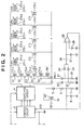
- FIG. 2 shows a circuit diagram of an inverter circuit configured with an odd number of drive transformers according to a second embodiment of the present invention.
- the same reference numerals are used to the same circuit components.
- a DC power source voltage Vin is applied between terminals T1 and T2.
- This DC power source voltage Vin is supplied to the control circuit 3 and the switching circuit 4 as DC operating voltages.
- the control circuit 3 in FIG. 3 is configured as same as the control circuit 3 in FIG. 1, so that the description thereof is neglected.
- the inverter circuit according to this second embodiment is configured with five drive transformers DT1 to DT5, five balancer-transformers CT1 to CT5, and one feedback transformer FBT. As shown in FIG. 2, secondary coils CT1-2 to CT5-2 of the five balancer-transformers CT1 to CT5 and a primary coil FBT-1 of the feedback transformer FBT are connected in series. Further, both ends of the series connection are connected to the pair of the output terminals of the switching circuit 4, and high frequency drive signals are applied thereto.
- the primary coil DT1-1 of the drive transformer DT1 and the primary coil CT1-1 of the balancer-transformer CT1 are connected in series, and both ends of the series-connection are connected to the pair of the output terminals of the switching circuit 4.
- the primary coil DT2-1 of the drive transformer DT2 and the primary coil CT2-1 of the balancer-transformer CT2 are connected in series, and both ends of the series-connection are connected to the pair of the output terminals of the switching circuit 4.
- the primary coil DT3-1 of the drive transformer DT3 and the primary coil CT3-1 of the balancer-transformer CT3 are connected in series, and both ends of the series-connection are connected to the pair of the output terminals of the switching circuit 4.
- the primary coil DT4-1 of the drive transformer DT4 and the primary coil CT4-1 of the balancer-transformer CT4 are connected in series, and both ends of the series-connection are connected to the pair of the output terminals of the switching circuit 4.
- the primary coil DT5-1 of the drive transformer DT5 and the primary coil CT5-1 of the balancer-transformer CT5 are connected in series, and both ends of the series-connection are connected to the pair of the output terminals of the switching circuit 4.
- the high frequency drive signals are generated at the secondary coils DT1-2 to DT5-2 of the drive transformers DT1 to DT5, and drive connected discharge tubes, respectively.
- these connections are well-known, so that they are neglected in the figure.
- the anode of the diode 5 is connected to one of terminals of the secondary coil FBT-2 in the feedback transformer FBT, and the cathode of the diode 5 is connected to ground by way of series-connected two resistors 6 and 7.
- the capacitor 8 for a rectifier operation is connected between the connecting midpoint of the two resistors 6 and 7 and the ground.
- the other terminal of the secondary coil FBT-2 is connected to ground.
- control circuit 3 controls an oscillation frequency of the oscillator circuit provided inside or width of pulse signals in accordance with the voltage supplied to this IF/B terminal. Thereby, it is controlled so that a current value of the high frequency drive signals flowing through the series-connection circuit of the secondary coils CT1-2 to CT5-2 of the five balancer-transformers CT1 to CT5 and the primary coil FBT-1 of the feedback transformer FBT becomes constant. Thereby, the discharge tubes connected to the secondary coils DT1-2 to DT5-2 of the drive transformers DT1 to DT 5 emit lights with a constant brightness.
- a feedback circuit using this feedback transformer FBT may directly detect current flowing through any one of a plurality of discharge tubes connected to the secondary coils DT1-2 to DT5-2 of the drive transformers DT1 to DT5. On this occasion, the feedback transformer FBT is not necessary.
- the connecting-midpoint between a secondary coil CT2-2 of the balancer-transformer CT2 and a secondary coil CT3-2 of the balancer-transformer CT3 is connected to ground by way of a series-connection circuit of a capacitor 20 and a resistor 22.
- the series-connection circuit of the capacitor 20 and the resistor 22 is also connected to an anode of a diode 25.
- a connecting-midpoint between a secondary coil CT3-2 of the balancer transformer CT3 and a secondary coil CT4-2 of the balancer-transformer CT4 is connected to ground by way of a series-connection circuit of a capacitor 21 and a resistor 23.
- the series-connection circuit of the capacitor 21 and the resistor 23 is also connected to an anode of a diode 24.
- a cathode of the diode 25 is connected to ground by way of a resistor 26 and a capacitor 27, and a connecting-midpoint between the resistor 26 and the capacitor 27 is connected to an - input terminal of a comparator circuit 29.
- a + input terminal of the comparator circuit 29 is supplied with a reference voltage (Vref) 28.
- Vref reference voltage
- a cathode of the diode 24 is commonly connected to the cathode of the diode 25.
- An output of the comparator circuit 29 is mixed with the voltage obtained at the connecting-midpoint between two resistors 6 and 7, and supplied to the IF/B terminal of the control circuit 3.
- the connecting-midpoint between the cathodes of the diode 24 and the diode 25 becomes a predetermined potential.
- the connecting-midpoint between the cathodes of the diode 24 and the diode 25 widely vary from the predetermined potential in the normal operation. This change is detected by the comparator circuit 29, and is supplied to the IF/B terminal of the control circuit 3.
- the second embodiment of the present invention it is able to detect the abnormal operation with only a single comparator circuit in spite of using an odd number of drive transformers and emitting control of odd number of discharge tubes. In this case, it is possible to apply the second embodiment if the number of drive transformers is three or more of an odd number.
- the detection of the voltages by the diodes 24 and 25 may be detected at two points such as at a connecting-midpoint between a ((k-1/2)th secondary coil and a ((K+1)/2)th secondary coil and at a connecting-midpoint between a ((k+1)/2)th secondary coil and a ((k+3)/2)th secondary coil.
- FIGS. 1 and 2 are examples of the present invention, and it is possible to modify these examples without departing from a spirit of the present invention.
Landscapes
- Circuit Arrangements For Discharge Lamps (AREA)
- Inverter Devices (AREA)
Abstract
Description
- The present invention relates to inverter circuits that control emission of discharge tubes such as fluorescent lights, and particularly to inverter circuits that are able to realize controls in case of abnormal operations such as an open-circuited load abnormality, a short-circuited load abnormality, and the like with a reduced number of circuit components.
- As well-known, a discharge tube such as a fluorescent light emits light by driven with high frequency drive signals generated by an inverter circuit. This type of discharge tube is not only used for lighting purpose, but recently also frequently used for a light source of a backlight employed in a liquid crystal display apparatus. An inverter circuit and discharge tubes are configured such that a drive transformer is provided at an output side of an inverter included in the inverter circuit, and a fluorescent light is connected to a secondary coil terminal of the drive transformer by way of connectors.
- However, it happens sometimes that the fluorescent light is not connected to the secondary coil terminal due to some defects in the connection terminals. Or, if output terminals of the secondary coils of the drive transformer are short-circuited with some reason, discharges may occur at the drive transformer by the high voltages, this may causes problems of smoking, firing, and the like. Other than the above-mentioned reason, if the fluorescent light breaks, or expires its life, output terminals of the secondary coils of the drive transformer connected to the fluorescent light become an open-circuited or a shot-circuited condition, so that this also cause above-mentioned problems of smoking, firing, and the like.
- Accordingly, in the inverter circuit, it is necessary to avoid any heating up state in case of the abnormal operations such as the open-circuited load condition, short-circuited load condition. For the sake, conventionally, it is common to provide an abnormality operation detecting circuit that detects an open condition or short-circuited condition of the output terminals of the secondary coils in the inverter, and stops the operation of the inverter in case of the abnormal operation.
- It is possible to detect current flowing through a discharge tube by connecting a detecting resistor at a low voltage side of the fluorescent light and by detecting the voltage across the resistor. Accordingly, the current flowing through the discharge tube is controlled to be constant by forming a feedback loop for the voltage across the resistor. Further, there are provided with an over-voltage protection circuit and an over-current protection circuit in the inverter circuit, which operate in case of abnormality in the discharge tubes.
- For example,
Japanese Patent Laid-open No. 2005-310587 - However, it is necessary to provide the same number of abnormality detecting circuits as the number of the discharge tubes in the afore-mentioned conventional inverter circuit. Thereby, in case of inverter circuits for driving discharge tubes used in a larger LCD TV, the number of discharge tubes increases, so that the cost for the abnormality detecting circuits also resultantly increase. The conventional abnormality detecting circuit detects an increase of the detecting voltage when the discharge tube becomes an open-circuited condition, and detects the decrease of the detecting voltage when the discharge tube becomes a short-circuited condition. Accordingly, it is necessary to employ a circuit called a window comparator system. This window comparator circuit detects whether the detected voltage is between the upper limit and the lower limit or not. For the sake, this window comparator circuit requires two comparators. This also increases resultantly the number of components and costs.
- Accordingly, this invention provides an inverter circuit for driving a plurality of discharge tubes, which is equipped with a protection circuit configured with a reduced number of components.
- An inverter circuit according to an embodiment of the present invention is an inverter circuit having plural sets of a drive transformer and a balancer-transformer, wherein a primary coil of the drive transformer and a primary coil of the balancer-transformer are connected in series, both ends of each of the series-connections of the plural sets are connected in parallel between output terminals of a switching circuit, and secondary coils of all the balancer-transformers of the plural sets are connected in series and connected between the output terminals of the switching circuit, the inverter circuit comprises:
- voltage detecting means for detecting a voltage at any of a connecting-midpoint of the series-connected secondary coils of the balancer-transformers; and
- voltage comparing means for comparing the voltage at any of the connecting-midpoint of the series-connected secondary coils of the balancer-transformers with a reference voltage, wherein
- the voltage comparing means outputs a signal indicating an abnormal operation when the voltage at the any of the connecting-midpoint exceeds the reference voltage.
- An inverter circuit according to another embodiment of the present invention is an inverter circuit which comprises:
- a switching circuit;
- n (n is 1, 2, 3,,,) series-connecting circuits in each of which a primary coil of a drive transformer and a primary coil of a balancer-transformer are connected in series; and
- a secondary coil series connecting circuit in which secondary coils of n balancer-transformers used in the n series connecting circuits are connected in series, wherein
- the n series-connecting circuits and the secondary coil series connecting circuit are connected in parallel between output terminals of the switching circuit.
- According the present invention, it is possible to provide an inverter circuit for a plurality of discharge tubes, which is equipped with a protection circuit configured with a reduced number of components.
- Further features of the present invention will become apparent from the following description of exemplary embodiments with reference to the attached drawings.
-
- FIG. 1 is a circuit diagram of an inverter circuit employing an even number of drive transformers according to a first embodiment of the present invention, and
- FIG. 2 is a circuit diagram of an inverter circuit employing an odd number of drive transformers according to a second embodiment of the present invention.
- FIG. 1 shows a circuit diagram of an inverter circuit configured with an even number of drive transformers according to a first embodiment of the present invention. In the inverter circuit in FIG. 1, a DC power source voltage Vin is supplied between
terminals control circuit 3 and aswitching circuit 4 as DC operating voltages. - The
control circuit 3 includes an oscillation circuit inside, and supplies switching pulses to theswitching circuit 4. Then, theswitching circuit 4 carries out switching of the DC power source voltage Vin to generate high frequency drive signals. On this account, theswitching circuit 4 is configured with a plurality of switching devices such as bi-polar or FET transistors. - Further, the inverter circuit in FIG. 1 is configured with four drive transformers DT1 to DT4, four balancer-transformers CT1 to CT4, and one feedback transformer FBT. AS shown in FIG. 1, secondary coils CT1-2 to CT4-2 of the four balancer-transformers CT1 to CT4 and a primary coil FBT-1 of the feedback transformer FBT are connected in series. Both ends of the series-connection circuit are connected to a pair of output terminals of the
switching circuit 4, and the high frequency drive signals are applied thereto from theswitching circuit 4. - Further, a primary coil DT1-1 of the drive transformer DT1 and a primary coil CT1-1 of the balancer-transformer CT1 are connected in series, and both end of the series-connection circuit are connected to the pair of the output terminals of the
switching circuit 4. - In addition, a primary coil DT2-1 of the drive transformer DT2 and a primary coil CT2-1 of the balancer-transformer CT2 are connected in series, and both ends of the series-connection circuit are connected to the pair of the output terminals of the
switching circuit 4. - In addition, a primary coil DT3-1 of the drive transformer DT3 and a primary coil CT3-1 of a balancer-transformer CT3 are connected in series, and both ends of the series-connection circuit are connected to the pair of the output terminals of the
switching circuit 4. - In addition, a primary coil DT4-1 of the drive transformer DT4 and a primary coil CT4-1 of the balancer-transformer CT4 are connected in series, and both ends of the series-connection circuit are connected to the pair of the output terminals of the
switching circuit 4. - Further, as well-known, the high frequency drive signals are generated at the secondary coils DT1-2 to DT4-2 of the drive transformers DT1 to DT4, and drive connected discharge tubes, respectively. However, these connections are well-known, so that they are neglected in the figure.
- In addition, an anode of a
diode 5 is connected to one of terminals of a secondary coil FBT-2 in the feedback transformer FBT, and a cathode of thediode 5 is connected to ground by way of series-connected tworesistors capacitor 8 for a rectifier operation is connected between a connecting-midpoint of the tworesistors - By the configuration as above described, at the connecting-midpoint of the two
resistors control circuit 3. - The
control circuit 3 controls an oscillation frequency of the oscillator circuit provided inside or width of pulse signals in accordance with the voltage supplied to this IF/B terminal. Thereby, it is controlled so that a current value of the high frequency drive signals flowing through the series-connection circuit of the secondary coils CT1-2 to CT4-2 of the four balancer-transformers CT1 to CT4 and the primary coil FBT-1 of the feedback transformer FBT becomes constant. Thereby, the discharge tubes connected to the secondary coils DT1-2 to DT4-2 of the drive transformers DT1 toDT 4 emit lights with a constant brightness. - In this case, a feedback circuit using this feedback transformer FBT may directly detect current flowing through any one of a plurality of discharge tubes connected to the secondary coils DT1-2 to DT4-2 of the drive transformers DT1 to DT4. On this occasion, the feedback transformer FBT is not necessary.
- Further, a connecting midpoint between a secondary coil CT2-2 of the balancer-transformer CT2 and a secondary coil CT3-2 of the balancer-transformer CT3 is connected to ground by way of a series-connection circuit of a
capacitor 9 and aresistor 10. The series-connection circuit of a connecting-midpoint between thecapacitor 9 and theresistor 10 is also connected to an anode of adiode 11. A cathode of thediode 11 is connected to ground by way of aresistor 12 and acapacitor 13, and a connecting-midpoint between theresistor 12 and thecapacitor 13 is connected to an - input terminal of acomparator circuit 14. A + input terminal of thecomparator circuit 14 is supplied with a reference voltage (Vref) 15. - An output of the
comparator circuit 14 is mixed with the voltage obtained at the connecting-midpoint between tworesistors control circuit 3. In the inverter circuit shown in FIG. 1, when normally operated, the connecting-midpoint between the secondary coil CT2-2 of the balancer-transformer CT2 and the secondary coil CT3-2 of the balancer-transformer CT3 becomes approximately 0 potential. - However, any one of the discharge tubes breaks, expires its life, or becomes improper connection, the connecting-midpoint between the secondary coil CT2-2 of the balancer-transformer CT2 and the secondary coil CT3-2 of the balancer-transformer CT3 widely vary from the 0 potential. This change is detected by the
comparator circuit 14, and is supplied to the IF/B terminal of thecontrol circuit 3. - When the inverter circuit normally operates, the
comparator circuit 14 may show high impedance by using an open-collector type circuit. By the way, in the above description, it is described that when normally operated, the connecting-midpoint between the secondary coil CT2-2 of the balancer-transformer CT2 and the secondary coil CT3-2 of the balancer-transformer CT3 becomes approximately 0 potential.
However, it is normal that circuit components include some fluctuations, so that some levels of tolerance are provided by using the reference voltage (Vref) 15. - Accordingly, any one of the connected discharge tubes breaks, expires its life, or becomes improper connection, and the voltage supplied to the - input terminal of the
comparator circuit 14 increases to above the reference voltage (Vref) 15, then, the output of thecomparator circuit 14 becomes ground potential, and the abnormal operation is to be detected. If the IF/B terminal of thecontrol circuit 3 becomes ground potential, thecontrol circuit 3 is so configured as to stop its operation. - According to the inverter circuit of the first embodiment of the present invention, it is able to detect the abnormal operation with only a single comparator circuit in spite of using a plurality of drive transformers and emitting control to a plurality of discharge tubes. In this case, it is possible to apply the first embodiment if the number of drive transformers is two or more of an even number. That is, if the number of secondary coils of balancer-transformers is j (j is an even number), the detection of the voltage by the
diode 11 may be detected at a connecting-midpoint between a (j/2)th secondary coil and a ((j/2)+1)th secondary coil. - FIG. 2 shows a circuit diagram of an inverter circuit configured with an odd number of drive transformers according to a second embodiment of the present invention. In this case, the same reference numerals are used to the same circuit components. Like the inverter circuit in FIG. 1, a DC power source voltage Vin is applied between terminals T1 and T2. This DC power source voltage Vin is supplied to the
control circuit 3 and theswitching circuit 4 as DC operating voltages. - The
control circuit 3 in FIG. 3 is configured as same as thecontrol circuit 3 in FIG. 1, so that the description thereof is neglected. - The inverter circuit according to this second embodiment is configured with five drive transformers DT1 to DT5, five balancer-transformers CT1 to CT5, and one feedback transformer FBT. As shown in FIG. 2, secondary coils CT1-2 to CT5-2 of the five balancer-transformers CT1 to CT5 and a primary coil FBT-1 of the feedback transformer FBT are connected in series.
Further, both ends of the series connection are connected to the pair of the output terminals of theswitching circuit 4, and high frequency drive signals are applied thereto. - In addition, the primary coil DT1-1 of the drive transformer DT1 and the primary coil CT1-1 of the balancer-transformer CT1 are connected in series, and both ends of the series-connection are connected to the pair of the output terminals of the
switching circuit 4. - Similarly, the primary coil DT2-1 of the drive transformer DT2 and the primary coil CT2-1 of the balancer-transformer CT2 are connected in series, and both ends of the series-connection are connected to the pair of the output terminals of the
switching circuit 4. - In addition, the primary coil DT3-1 of the drive transformer DT3 and the primary coil CT3-1 of the balancer-transformer CT3 are connected in series, and both ends of the series-connection are connected to the pair of the output terminals of the
switching circuit 4. - In addition, the primary coil DT4-1 of the drive transformer DT4 and the primary coil CT4-1 of the balancer-transformer CT4 are connected in series, and both ends of the series-connection are connected to the pair of the output terminals of the
switching circuit 4. - In addition, the primary coil DT5-1 of the drive transformer DT5 and the primary coil CT5-1 of the balancer-transformer CT5 are connected in series, and both ends of the series-connection are connected to the pair of the output terminals of the
switching circuit 4. - Further, as well-known, the high frequency drive signals are generated at the secondary coils DT1-2 to DT5-2 of the drive transformers DT1 to DT5, and drive connected discharge tubes, respectively. However, these connections are well-known, so that they are neglected in the figure.
- In addition, the anode of the
diode 5 is connected to one of terminals of the secondary coil FBT-2 in the feedback transformer FBT, and the cathode of thediode 5 is connected to ground by way of series-connected tworesistors capacitor 8 for a rectifier operation is connected between the connecting midpoint of the tworesistors resistors control circuit 3. - Accordingly, the
control circuit 3 controls an oscillation frequency of the oscillator circuit provided inside or width of pulse signals in accordance with the voltage supplied to this IF/B terminal. Thereby, it is controlled so that a current value of the high frequency drive signals flowing through the series-connection circuit of the secondary coils CT1-2 to CT5-2 of the five balancer-transformers CT1 to CT5 and the primary coil FBT-1 of the feedback transformer FBT becomes constant. Thereby, the discharge tubes connected to the secondary coils DT1-2 to DT5-2 of the drive transformers DT1 toDT 5 emit lights with a constant brightness. - In this case, a feedback circuit using this feedback transformer FBT may directly detect current flowing through any one of a plurality of discharge tubes connected to the secondary coils DT1-2 to DT5-2 of the drive transformers DT1 to DT5. On this occasion, the feedback transformer FBT is not necessary.
- Further, the connecting-midpoint between a secondary coil CT2-2 of the balancer-transformer CT2 and a secondary coil CT3-2 of the balancer-transformer CT3 is connected to ground by way of a series-connection circuit of a
capacitor 20 and aresistor 22. The series-connection circuit of thecapacitor 20 and theresistor 22 is also connected to an anode of adiode 25. - Similarly, a connecting-midpoint between a secondary coil CT3-2 of the balancer transformer CT3 and a secondary coil CT4-2 of the balancer-transformer CT4 is connected to ground by way of a series-connection circuit of a
capacitor 21 and aresistor 23. The series-connection circuit of thecapacitor 21 and theresistor 23 is also connected to an anode of adiode 24. - A cathode of the
diode 25 is connected to ground by way of aresistor 26 and acapacitor 27, and a connecting-midpoint between theresistor 26 and thecapacitor 27 is connected to an - input terminal of acomparator circuit 29. A + input terminal of thecomparator circuit 29 is supplied with a reference voltage (Vref) 28. Further, a cathode of thediode 24 is commonly connected to the cathode of thediode 25. - An output of the
comparator circuit 29 is mixed with the voltage obtained at the connecting-midpoint between tworesistors control circuit 3. In the inverter circuit shown in FIG. 2, when normally operated, the connecting-midpoint between the cathodes of thediode 24 and thediode 25 becomes a predetermined potential. However, once any of the discharge tubes breaks, expires its life, or becomes improper connection, the connecting-midpoint between the cathodes of thediode 24 and thediode 25 widely vary from the predetermined potential in the normal operation. This change is detected by thecomparator circuit 29, and is supplied to the IF/B terminal of thecontrol circuit 3. - Accordingly, once any of the connected discharge tubes breaks, expires its life, or becomes improper connection, and the voltage supplied to the - input terminal of the
comparator circuit 29 increases to above the reference voltage (Vref) 28, then, the output of thecomparator circuit 29 becomes ground potential, and the abnormal operation is to be detected. If the IF/B terminal of thecontrol circuit 3 becomes ground potential, thecontrol circuit 3 is so configured as to stop its operation. - According to the second embodiment of the present invention, it is able to detect the abnormal operation with only a single comparator circuit in spite of using an odd number of drive transformers and emitting control of odd number of discharge tubes. In this case, it is possible to apply the second embodiment if the number of drive transformers is three or more of an odd number. Namely, if the number of the secondary coils of balancer-transformers is k (k is an odd number), the detection of the voltages by the
diodes - The inverter circuits shown in FIGS. 1 and 2 are examples of the present invention, and it is possible to modify these examples without departing from a spirit of the present invention.
- While the present invention has been described with reference to exemplary embodiments, it is to be understood that the invention is not limited to the disclosed exemplary embodiments. The scope of the following claims is to be accorded the broadest interpretation so as to encompass all such modifications and equivalent structures and functions.
Claims (9)
- An inverter circuit having plural sets of a drive transformer and a balancer-transformer, wherein a primary coil of the drive transformer and a primary coil of the balancer-transformer are connected in series, both ends of each of the series-connections of the plural sets are connected in parallel between output terminals of a switching circuit, and secondary coils of all the balancer-transformers of the plural sets are connected in series and connected between the output terminals of the switching circuit, the inverter circuit comprising:voltage detecting means for detecting a voltage at any of a connecting-midpoint of the series-connected secondary coils of the balancer-transformers; andvoltage comparing means for comparing the voltage at any of the connecting-midpoint of the series-connected secondary coils of the balancer-transformers with a reference voltage, whereinthe voltage comparing means outputs a signal indicating an abnormal operation when the voltage at said any of the connecting-midpoint exceeds the reference voltage.
- The inverter circuit according to claim 1, wherein
the voltage comparing means includes a comparator circuit, in which the voltage at the any of the connecting-midpoint of the series-connected secondary coils of the balancer-transformers is connected to a-input terminal of the comparator circuit, and the reference voltage is connected to a + input terminal of the comparator circuit. - The inverter circuit according to claim 1 or 2, wherein
the voltage detecting means detects the voltage from the connecting-midpoint between the (j/2) th secondary coil and the ((j/2)+1)th secondary coil which is the series-connected secondary coil of the balancer-transformer, where j is a positive even integer. - The inverter circuit according to claim 1 or 2, wherein
the voltage detecting means detects the voltage from the connecting-midpoint between the ((k-1)/2)th secondary coil and the ((k+1)/2)th secondary coil and from the connecting-midpoint between the ((k+1) /2) th secondary coil and ((k+3)/2)th secondary coil which is the series-connected secondary coils of the balancer-transformer, where k is a positive odd integer. - An inverter circuit comprising:a switching circuit;n (n is 1, 2, 3,,,) series-connecting circuits in each of which a primary coil of a drive transformer and a primary coil of a balancer-transformer are connected in series; anda secondary coil series connecting circuit in which secondary coils of n balancer-transformers used in the n series connecting circuits are connected in series, whereinthe n series-connecting circuits and the secondary coil series connecting circuit are connected in parallel between output terminals of the switching circuit.
- The inverter circuit according to claim 5, further comprising:voltage detecting means for detecting a voltage at the secondary coil series connecting circuit.
- The inverter circuit according to claim 6, further comprising:comparing means for comparing the voltage detected at the secondary coil series connecting circuit with a reference voltage, whereinthe comparing means outputs a signal indicating an abnormal operation when the voltage exceeds the reference voltage.
- The inverter circuit according to claim 6 or 7, wherein
the voltage detecting means detects the voltage from the connecting-midpoint between the (j/2) th secondary coil and the ((j/2)+1)th secondary coil which is secondary coil series connecting circuit, where j is a positive even integer. - The inverter circuit according to claim 6 or 7, wherein
the voltage detecting means detects the voltage from the connecting-midpoint between the ((k-1)/2)th secondary coil and the ((k+1)/2)th secondary coil and from the connecting-midpoint between the ((k+1)/2) th secondary coil and ((k+3)/2) th secondary coil which is the secondary coil series connecting circuit, where k is a positive odd integer.
Applications Claiming Priority (1)
| Application Number | Priority Date | Filing Date | Title |
|---|---|---|---|
| JP2006205260A JP4584880B2 (en) | 2006-07-27 | 2006-07-27 | Inverter circuit |
Publications (3)
| Publication Number | Publication Date |
|---|---|
| EP1885165A2 true EP1885165A2 (en) | 2008-02-06 |
| EP1885165A3 EP1885165A3 (en) | 2009-07-15 |
| EP1885165B1 EP1885165B1 (en) | 2014-03-26 |
Family
ID=38630095
Family Applications (1)
| Application Number | Title | Priority Date | Filing Date |
|---|---|---|---|
| EP07011158.8A Ceased EP1885165B1 (en) | 2006-07-27 | 2007-06-06 | Inverter Circuit |
Country Status (6)
| Country | Link |
|---|---|
| US (1) | US7515443B2 (en) |
| EP (1) | EP1885165B1 (en) |
| JP (1) | JP4584880B2 (en) |
| KR (1) | KR100882001B1 (en) |
| CN (1) | CN101115340B (en) |
| TW (1) | TW200808127A (en) |
Families Citing this family (4)
| Publication number | Priority date | Publication date | Assignee | Title |
|---|---|---|---|---|
| US20090059455A1 (en) * | 2007-08-31 | 2009-03-05 | Texas Instruments Incorporated | Method and apparatus for power interruption protection |
| US9770060B2 (en) * | 2013-02-12 | 2017-09-26 | Riddell, Inc. | Pad assemblies for a protective sports helmet |
| TWI742404B (en) | 2018-07-19 | 2021-10-11 | 新加坡商聯發科技(新加坡)私人有限公司 | Detecting foreign objects in wireless power transfer systems |
| CN110945745B (en) | 2018-07-19 | 2023-09-01 | 联发科技(新加坡)私人有限公司 | Foreign Object Detection in Wireless Power Transfer Systems |
Citations (2)
| Publication number | Priority date | Publication date | Assignee | Title |
|---|---|---|---|---|
| US20050093472A1 (en) | 2003-10-06 | 2005-05-05 | Xiaoping Jin | Balancing transformers for ring balancer |
| US20050225261A1 (en) | 2004-04-07 | 2005-10-13 | Xiaoping Jin | Primary side current balancing scheme for multiple CCF lamp operation |
Family Cites Families (10)
| Publication number | Priority date | Publication date | Assignee | Title |
|---|---|---|---|---|
| JPS6431394A (en) * | 1987-07-27 | 1989-02-01 | Matsushita Electric Works Ltd | Discharge lamp lighting device |
| US7002304B2 (en) * | 2004-01-02 | 2006-02-21 | Lien Chang Electronic Enterprise Co., Ltd. | Multi-lamp drive device |
| JP2005310587A (en) | 2004-04-22 | 2005-11-04 | Hitachi Media Electoronics Co Ltd | Discharge lamp lighting device |
| JP4649127B2 (en) | 2004-06-14 | 2011-03-09 | キヤノン株式会社 | Capacitor charging circuit, imaging device and strobe device |
| JP2006066220A (en) | 2004-08-26 | 2006-03-09 | Mitsumi Electric Co Ltd | Cold cathode tube drive circuit |
| JP2006156338A (en) * | 2004-11-05 | 2006-06-15 | Taiyo Yuden Co Ltd | Lamp lighting device |
| JP4529132B2 (en) | 2004-12-24 | 2010-08-25 | ミネベア株式会社 | Multi-lamp type discharge lamp lighting device |
| US20060244395A1 (en) * | 2005-05-02 | 2006-11-02 | Taipale Mark S | Electronic ballast having missing lamp detection |
| US7271549B2 (en) * | 2005-06-07 | 2007-09-18 | Au Optronics Corporation | Current balancing circuit for a multi-lamp system |
| TWM314499U (en) * | 2006-11-07 | 2007-06-21 | Lite On Technology Corp | Protecton apparatus and multi-lamp driving system using the same |
-
2006
- 2006-07-27 JP JP2006205260A patent/JP4584880B2/en not_active Expired - Fee Related
-
2007
- 2007-06-06 EP EP07011158.8A patent/EP1885165B1/en not_active Ceased
- 2007-06-12 US US11/761,474 patent/US7515443B2/en not_active Expired - Fee Related
- 2007-06-21 TW TW096122281A patent/TW200808127A/en not_active IP Right Cessation
- 2007-07-26 KR KR1020070075083A patent/KR100882001B1/en not_active Expired - Fee Related
- 2007-07-27 CN CN2007101296277A patent/CN101115340B/en not_active Expired - Fee Related
Patent Citations (2)
| Publication number | Priority date | Publication date | Assignee | Title |
|---|---|---|---|---|
| US20050093472A1 (en) | 2003-10-06 | 2005-05-05 | Xiaoping Jin | Balancing transformers for ring balancer |
| US20050225261A1 (en) | 2004-04-07 | 2005-10-13 | Xiaoping Jin | Primary side current balancing scheme for multiple CCF lamp operation |
Also Published As
| Publication number | Publication date |
|---|---|
| CN101115340B (en) | 2011-11-02 |
| US20080025055A1 (en) | 2008-01-31 |
| TWI372579B (en) | 2012-09-11 |
| JP2008034206A (en) | 2008-02-14 |
| KR100882001B1 (en) | 2009-02-04 |
| CN101115340A (en) | 2008-01-30 |
| EP1885165A3 (en) | 2009-07-15 |
| JP4584880B2 (en) | 2010-11-24 |
| US7515443B2 (en) | 2009-04-07 |
| EP1885165B1 (en) | 2014-03-26 |
| KR20080011086A (en) | 2008-01-31 |
| TW200808127A (en) | 2008-02-01 |
Similar Documents
| Publication | Publication Date | Title |
|---|---|---|
| KR20160019934A (en) | Led backlight and liquid crystal display | |
| US6710555B1 (en) | Discharge lamp lighting circuit with protection circuit | |
| US8102124B2 (en) | Inverter circuit for light source | |
| US7515443B2 (en) | Inverter circuit | |
| US9468071B2 (en) | Switching power supply device and projection video display device | |
| CN1770946B (en) | lighting device | |
| JP2012060744A (en) | Drive circuit of light emitting element, light emitting device using the same, and electronic apparatus | |
| CN100558212C (en) | Lamp driving device and driving method of liquid crystal display device | |
| EP1718132B1 (en) | Load failure protection circuit and discharge lamp driving apparatus | |
| US8159141B2 (en) | Methods and apparatus for driving discharge lamps | |
| US8436540B2 (en) | Multi-lamp driving system | |
| US8436547B2 (en) | Multi-lamp driving system | |
| US7525260B2 (en) | Discharge lamp lighting apparatus | |
| US7372211B2 (en) | Cold cathode tube lighting device and driving method and integrated circuit to be used in same | |
| US20090045757A1 (en) | Discharge lamp lighter | |
| US7781989B2 (en) | Discharge lamp drive control circuit | |
| US7579789B2 (en) | Device for driving light sources | |
| US20090160355A1 (en) | Discharge Lamp Lighting Apparatus | |
| JP4950442B2 (en) | Fluorescent lamp driving device, light emitting device and liquid crystal television | |
| US20070200507A1 (en) | Device for driving light source module | |
| JP4479918B2 (en) | Discharge lamp lighting device | |
| JP2006066220A (en) | Cold cathode tube drive circuit | |
| JP5195020B2 (en) | Light source element lighting device | |
| JP2010040208A (en) | Backlight device for liquid crystal panel | |
| JP2007141752A (en) | Step-up transformer, discharge lamp lighting circuit, discharge lamp device, and discharge lamp lighting method |
Legal Events
| Date | Code | Title | Description |
|---|---|---|---|
| PUAI | Public reference made under article 153(3) epc to a published international application that has entered the european phase |
Free format text: ORIGINAL CODE: 0009012 |
|
| 17P | Request for examination filed |
Effective date: 20070809 |
|
| AK | Designated contracting states |
Kind code of ref document: A2 Designated state(s): AT BE BG CH CY CZ DE DK EE ES FI FR GB GR HU IE IS IT LI LT LU LV MC MT NL PL PT RO SE SI SK TR |
|
| AX | Request for extension of the european patent |
Extension state: AL BA HR MK YU |
|
| PUAL | Search report despatched |
Free format text: ORIGINAL CODE: 0009013 |
|
| AK | Designated contracting states |
Kind code of ref document: A3 Designated state(s): AT BE BG CH CY CZ DE DK EE ES FI FR GB GR HU IE IS IT LI LT LU LV MC MT NL PL PT RO SE SI SK TR |
|
| AX | Request for extension of the european patent |
Extension state: AL BA HR MK RS |
|
| AKX | Designation fees paid |
Designated state(s): DE FR GB |
|
| 17Q | First examination report despatched |
Effective date: 20121010 |
|
| GRAP | Despatch of communication of intention to grant a patent |
Free format text: ORIGINAL CODE: EPIDOSNIGR1 |
|
| INTG | Intention to grant announced |
Effective date: 20131011 |
|
| GRAS | Grant fee paid |
Free format text: ORIGINAL CODE: EPIDOSNIGR3 |
|
| GRAA | (expected) grant |
Free format text: ORIGINAL CODE: 0009210 |
|
| RAP1 | Party data changed (applicant data changed or rights of an application transferred) |
Owner name: SUMIDA CORPORATION |
|
| RIN1 | Information on inventor provided before grant (corrected) |
Inventor name: HATAKEYAMA, TAKESHI Inventor name: MIYAZAKI, HIROYUKI |
|
| AK | Designated contracting states |
Kind code of ref document: B1 Designated state(s): DE FR GB |
|
| REG | Reference to a national code |
Ref country code: GB Ref legal event code: FG4D |
|
| REG | Reference to a national code |
Ref country code: DE Ref legal event code: R096 Ref document number: 602007035736 Country of ref document: DE Effective date: 20140508 |
|
| RAP2 | Party data changed (patent owner data changed or rights of a patent transferred) |
Owner name: SUMIDA CORPORATION |
|
| REG | Reference to a national code |
Ref country code: DE Ref legal event code: R097 Ref document number: 602007035736 Country of ref document: DE |
|
| PLBE | No opposition filed within time limit |
Free format text: ORIGINAL CODE: 0009261 |
|
| STAA | Information on the status of an ep patent application or granted ep patent |
Free format text: STATUS: NO OPPOSITION FILED WITHIN TIME LIMIT |
|
| 26N | No opposition filed |
Effective date: 20150106 |
|
| REG | Reference to a national code |
Ref country code: DE Ref legal event code: R097 Ref document number: 602007035736 Country of ref document: DE Effective date: 20150106 |
|
| REG | Reference to a national code |
Ref country code: FR Ref legal event code: PLFP Year of fee payment: 9 |
|
| REG | Reference to a national code |
Ref country code: FR Ref legal event code: PLFP Year of fee payment: 10 |
|
| REG | Reference to a national code |
Ref country code: FR Ref legal event code: CA Effective date: 20160822 |
|
| REG | Reference to a national code |
Ref country code: FR Ref legal event code: PLFP Year of fee payment: 11 |
|
| REG | Reference to a national code |
Ref country code: FR Ref legal event code: PLFP Year of fee payment: 12 |
|
| PGFP | Annual fee paid to national office [announced via postgrant information from national office to epo] |
Ref country code: DE Payment date: 20190619 Year of fee payment: 13 |
|
| PGFP | Annual fee paid to national office [announced via postgrant information from national office to epo] |
Ref country code: FR Payment date: 20190619 Year of fee payment: 13 |
|
| PGFP | Annual fee paid to national office [announced via postgrant information from national office to epo] |
Ref country code: GB Payment date: 20190619 Year of fee payment: 13 |
|
| REG | Reference to a national code |
Ref country code: DE Ref legal event code: R119 Ref document number: 602007035736 Country of ref document: DE |
|
| GBPC | Gb: european patent ceased through non-payment of renewal fee |
Effective date: 20200606 |
|
| PG25 | Lapsed in a contracting state [announced via postgrant information from national office to epo] |
Ref country code: FR Free format text: LAPSE BECAUSE OF NON-PAYMENT OF DUE FEES Effective date: 20200630 Ref country code: GB Free format text: LAPSE BECAUSE OF NON-PAYMENT OF DUE FEES Effective date: 20200606 |
|
| PG25 | Lapsed in a contracting state [announced via postgrant information from national office to epo] |
Ref country code: DE Free format text: LAPSE BECAUSE OF NON-PAYMENT OF DUE FEES Effective date: 20210101 |