EP1885053A2 - Power supply circuit - Google Patents
Power supply circuit Download PDFInfo
- Publication number
- EP1885053A2 EP1885053A2 EP07252920A EP07252920A EP1885053A2 EP 1885053 A2 EP1885053 A2 EP 1885053A2 EP 07252920 A EP07252920 A EP 07252920A EP 07252920 A EP07252920 A EP 07252920A EP 1885053 A2 EP1885053 A2 EP 1885053A2
- Authority
- EP
- European Patent Office
- Prior art keywords
- light
- circuit
- photocoupler
- breakdown
- voltage
- Prior art date
- Legal status (The legal status is an assumption and is not a legal conclusion. Google has not performed a legal analysis and makes no representation as to the accuracy of the status listed.)
- Withdrawn
Links
- 230000015556 catabolic process Effects 0.000 claims abstract description 44
- 230000008878 coupling Effects 0.000 claims abstract description 3
- 238000010168 coupling process Methods 0.000 claims abstract description 3
- 238000005859 coupling reaction Methods 0.000 claims abstract description 3
- 238000001514 detection method Methods 0.000 description 15
- 238000009499 grossing Methods 0.000 description 9
- ATJFFYVFTNAWJD-UHFFFAOYSA-N Tin Chemical compound [Sn] ATJFFYVFTNAWJD-UHFFFAOYSA-N 0.000 description 8
- 238000010586 diagram Methods 0.000 description 6
- 239000003990 capacitor Substances 0.000 description 5
- 238000009413 insulation Methods 0.000 description 2
- 230000007423 decrease Effects 0.000 description 1
- 230000004048 modification Effects 0.000 description 1
- 238000012986 modification Methods 0.000 description 1
Images


Classifications
-
- H—ELECTRICITY
- H02—GENERATION; CONVERSION OR DISTRIBUTION OF ELECTRIC POWER
- H02M—APPARATUS FOR CONVERSION BETWEEN AC AND AC, BETWEEN AC AND DC, OR BETWEEN DC AND DC, AND FOR USE WITH MAINS OR SIMILAR POWER SUPPLY SYSTEMS; CONVERSION OF DC OR AC INPUT POWER INTO SURGE OUTPUT POWER; CONTROL OR REGULATION THEREOF
- H02M1/00—Details of apparatus for conversion
- H02M1/32—Means for protecting converters other than automatic disconnection
-
- H—ELECTRICITY
- H02—GENERATION; CONVERSION OR DISTRIBUTION OF ELECTRIC POWER
- H02M—APPARATUS FOR CONVERSION BETWEEN AC AND AC, BETWEEN AC AND DC, OR BETWEEN DC AND DC, AND FOR USE WITH MAINS OR SIMILAR POWER SUPPLY SYSTEMS; CONVERSION OF DC OR AC INPUT POWER INTO SURGE OUTPUT POWER; CONTROL OR REGULATION THEREOF
- H02M3/00—Conversion of DC power input into DC power output
- H02M3/22—Conversion of DC power input into DC power output with intermediate conversion into AC
- H02M3/24—Conversion of DC power input into DC power output with intermediate conversion into AC by static converters
- H02M3/28—Conversion of DC power input into DC power output with intermediate conversion into AC by static converters using discharge tubes with control electrode or semiconductor devices with control electrode to produce the intermediate AC
- H02M3/325—Conversion of DC power input into DC power output with intermediate conversion into AC by static converters using discharge tubes with control electrode or semiconductor devices with control electrode to produce the intermediate AC using devices of a triode or a transistor type requiring continuous application of a control signal
- H02M3/335—Conversion of DC power input into DC power output with intermediate conversion into AC by static converters using discharge tubes with control electrode or semiconductor devices with control electrode to produce the intermediate AC using devices of a triode or a transistor type requiring continuous application of a control signal using semiconductor devices only
- H02M3/33507—Conversion of DC power input into DC power output with intermediate conversion into AC by static converters using discharge tubes with control electrode or semiconductor devices with control electrode to produce the intermediate AC using devices of a triode or a transistor type requiring continuous application of a control signal using semiconductor devices only with automatic control of the output voltage or current, e.g. flyback converters
- H02M3/33523—Conversion of DC power input into DC power output with intermediate conversion into AC by static converters using discharge tubes with control electrode or semiconductor devices with control electrode to produce the intermediate AC using devices of a triode or a transistor type requiring continuous application of a control signal using semiconductor devices only with automatic control of the output voltage or current, e.g. flyback converters with galvanic isolation between input and output of both the power stage and the feedback loop
Definitions
- the present invention generally relates to a power supply circuit. More particularly, this invention relates to a power supply circuit where a primary circuit connected to a primary coil of a transformer and a secondary circuit connected to a secondary coil of the transformer are coupled by a photocoupler.
- a switched-mode power supply is used for an AC adaptor that converts an alternating current from, for example, a power line to a direct current and supplies the direct current to a device (see, for example, patent document 1).
- FIG. 3 is a circuit diagram illustrating an exemplary conventional switched-mode power supply circuit.
- a switched-mode power supply circuit 10 shown in FIG. 3 includes a primary circuit 11, a secondary circuit 12, a transformer 13, and a photocoupler 14.
- the primary circuit 11 includes a rectifying-smoothing circuit 21 and a control circuit 22.
- An alternating voltage is applied to input terminals Tin+ and Tin- of the primary circuit 11.
- the rectifying-smoothing circuit 21 rectifies and smoothes the alternating voltage applied to the input terminals Tin+ and Tin- and applies the smoothed voltage to one end of a primary coil L1 of the transformer 13.
- the other end of the primary coil L1 of the transformer 13 is connected to the control circuit 22.
- the control circuit 22 switches on and off the current flowing through the primary coil L1 at a duty cycle or a frequency corresponding to a detection signal supplied from the photocoupler 14
- the secondary circuit 12 includes a rectifying-smoothing circuit 31 and an output detection circuit 32.
- the rectifying-smoothing circuit 31 rectifies and smoothes the voltage appearing at both ends of the secondary coil L2 of the transformer 13 and outputs the voltage from output terminals Tout+ and Tout-.
- the output detection circuit 32 detects the voltage output from the output terminal Tout+, generates a detection signal corresponding to the output voltage, and thereby controls the photocoupler 14.
- the photocoupler 14 includes a light-emitting diode Dp and a phototransistor Qp.
- the light-emitting diode Dp is driven according to the detection signal from the output detection circuit 32 and emits an amount of light corresponding to the detection signal.
- the light emitted from the light-emitting diode Dp enters the phototransistor Qp.
- the phototransistor Qp draws an amount of current corresponding to the amount of light from the control circuit 22.
- the control circuit 22 switches on and off the current flowing through the primary coil L1 at a duty cycle or a frequency corresponding to the current drawn by the phototransistor Qp. In other words, the control circuit 22 switches on and off the current flowing through the primary coil L1 according to the detection signal from the output detection circuit 32 such that a constant voltage is output from the output terminals Tout+ and Tout-.
- the switched-mode power supply circuit 10 outputs a constant voltage from the output terminals Tout+ and Tout-.
- One problem with a conventional power supply circuit is that when an electrical breakdown occurs in a photocoupler (the photocoupler "breaks down"), the light-receiving element and the light-emitting element of the photocoupler short-circuit and insulation between the primary circuit and the secondary circuit may break down.
- Embodiments of the present invention provide a power supply circuit where a short circuit between a light-receiving element and a light-emitting element of a photocoupler is prevented and insulation between a primary circuit and a secondary circuit is maintained.
- a power supply circuit includes a transformer including a primary coil and a secondary coil; a primary circuit connected to the primary coil; a secondary circuit connected to the secondary coil; a photocoupler including a light-receiving element and a light-emitting element, the photocoupler coupling the primary circuit and the secondary circuit; and a breakdown element connected in parallel with the light-receiving element or the light-emitting element; wherein the breakdown element is configured to break down at or above a first voltage that is lower than a second voltage at or above which the light-receiving element or the light-emitting element breaks down and thereby to cause a short-circuit between terminals of the light-receiving element or the light-emitting element.
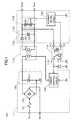
- FIG. 1 is a circuit diagram illustrating a power supply circuit according to an embodiment of the present invention.
- a power supply circuit 100 of this embodiment includes a primary circuit 111, a secondary circuit 112, a transformer 113, a photocoupler 114, and a breakdown element 115.
- the primary circuit 111 is connected to a primary coil L1 of the transformer 113 and includes a fuse 121, a diode rectifier circuit 122, a smoothing circuit 123, and a primary control circuit 124.
- An alternating voltage is applied between input terminals Tin+ and Tin-.
- the input terminal Tin+ is connected via the fuse 121 to the anode terminal of the diode rectifier circuit 122.
- the input terminal Tin- is connected directly to the cathode terminal of the diode rectifier circuit 122.
- the diode rectifier circuit 122 comprises a diode bridge circuit and rectifies the alternating voltage applied between the input terminals Tin+ and Tin-.
- the voltage rectified by the diode rectifier circuit 122 is applied to the smoothing circuit 123.
- the smoothing circuit 123 comprises a capacitor C11.
- the capacitor C11 is connected between output paths of the diode rectifier circuit 122.
- the capacitor C11 smoothes the voltage rectified by the diode rectifier circuit 122 and applies the smoothed voltage to one end of the primary coil L1 of the transformer 113.
- the other end of the primary coil L1 of the transformer 113 is connected to the primary control circuit 124.
- the primary control circuit 124 controls the electric current flowing through the primary coil L1 of the transformer 113 according to a detection signal supplied from the photocoupler 114. As a result, a voltage corresponding to the detection signal appears at a secondary coil L2 of the transformer 113.
- the secondary coil L2 is connected to the secondary circuit 112.
- the secondary circuit 112 includes a rectifying-smoothing circuit 131, an output voltage detection circuit 132, and a secondary control circuit 133.
- the rectifying-smoothing circuit 131 includes a diode D21 and a capacitor C21.
- the anode of the diode D21 is connected to one end of the secondary coil L2 and the cathode is connected to an output terminal Tout+.
- the diode D21 rectifies the voltage appearing at the secondary coil L2.
- the capacitor C21 is connected between output terminals Tout+ and Tout- and smoothes the output voltage.
- the output voltage detection circuit 132 is connected between the output terminals Tout+ and Tout-.
- the output voltage detection circuit 132 includes resistors R21 and R22 connected in series between the output terminals Tout+ and Tout-.
- a node between the resistors R21 and R22 is connected to the secondary control circuit 133.
- the output voltage detection circuit 132 obtains a fraction of the output voltage applied between the output terminals Tout+ and Tout-using the resistors R21 and R22 and supplies the fraction of the output voltage (detected voltage) to the secondary control circuit 133.
- the secondary control circuit 133 is connected to the photocoupler 114 and controls the photocoupler 114 according to the detected voltage supplied from the output voltage detecting circuit 132.
- the photocoupler 114 is implemented as a chip where a light-emitting diode Dp that is a light-emitting element and a phototransistor Qp that is a light-receiving element are integrated.
- the anode of the light-emitting diode Dp is connected via a terminal T21 to the output terminal Tout+ and the cathode is connected via a terminal T22 to the secondary control circuit 133.
- the amount of current flowing into the light-emitting diode Dp of the photocoupler 114 is controlled according to the detected voltage. Accordingly, the light-emitting diode Dp emits an amount of light corresponding to the detected voltage. The light emitted from the light-emitting diode Dp enters the phototransistor Qp.
- the collector of the phototransistor Qp draws an amount of current corresponding to the amount of received light from the primary control circuit 124.
- the collector of the phototransistor Qp of the photocoupler 114 is connected via a terminal T11 to the primary control circuit 124 and the emitter is connected via a terminal T12 to ground.
- the breakdown element 115 is connected between the terminals T11 and T12 to which the collector and the emitter of the phototransistor Qp are connected.
- the breakdown element 115 comprises a breakdown Zener diode and is provided as a separate electronic component near the photocoupler 114.
- the cathode of the breakdown element 115 is connected to the terminal T11 connected to the collector of the phototransistor Qp of the photocoupler 114 and the anode of the breakdown element 115 is connected to the terminal T12 connected to the emitter of the phototransistor Qp of the photocoupler 114.
- the breakdown Zener diode for example, has a withstand voltage of about 35 V. When an applied voltage reaches or exceeds 35 V, the breakdown Zener diode breaks down and, as a result, its cathode and anode short-circuit.
- the withstand voltage of the phototransistor Qp of the photocoupler 114 is, for example, set at about 50 V. In other words, the breakdown voltage of the breakdown Zener diode is lower than that of the phototransistor Qp of the photocoupler 114.
- the breakdown element 115 breaks down and short-circuits before the applied voltage reaches the withstand voltage of the phototransistor Qp. Short-circuiting the breakdown element 115 decreases the voltage applied to the phototransistor Qp and thereby prevents breakdown of the phototransistor Qp. This in turn prevents breakdown of the photocoupler 114.
- the above embodiment makes it possible to prevent breakdown of the photocoupler 114 resulting from, for example, supply voltage surge by just connecting the breakdown element 115 in parallel with the phototransistor Qp of the photocoupler 114.
- the above embodiment makes it possible to prevent breakdown of the photocoupler 114 with a simple configuration.
- the breakdown element 115 is connected between the collector and emitter of the phototransistor Qp of the photocoupler 114 which phototransistor Qp is closer to the power supply than the light-emitting diode Dp.
- the breakdown element 115 may be connected between the anode and cathode of the light-emitting diode Dp to prevent breakdown of the light-emitting diode Dp.
- FIG. 2 is a circuit diagram illustrating a power supply circuit according to another embodiment of the present invention.
- components corresponding to those shown in FIG. 1 are assigned the same reference numbers and descriptions of those components are omitted here.
- a breakdown element 211 is connected between the anode and cathode of the photodiode Dp of the photocoupler 114, in other words, between the terminals T21 and T22.
- the breakdown element 211 comprises a breakdown Zener diode and is provided as a separate electronic component near the photocoupler 114.
- the cathode of the breakdown element 211 is connected to the terminal T21 connected to the anode of the light-emitting diode Dp of the photocoupler 114 and the anode of the breakdown element 211 is connected to the terminal T22 connected to the cathode of the light-emitting diode Dp of the photocoupler 114.
- the breakdown voltage of the breakdown element 211 is lower than that of the light-emitting diode Dp of the photocoupler 114. In other words, the breakdown element 211 breaks down and short-circuits before the applied voltage reaches the breakdown voltage of the light-emitting diode Dp.
- this embodiment makes it possible to prevent breakdown of the light-emitting diode Dp resulting from an overvoltage and thereby to prevent breakdown of the photocoupler 114.
Landscapes
- Engineering & Computer Science (AREA)
- Power Engineering (AREA)
- Dc-Dc Converters (AREA)
Abstract
Description
- The present invention generally relates to a power supply circuit. More particularly, this invention relates to a power supply circuit where a primary circuit connected to a primary coil of a transformer and a secondary circuit connected to a secondary coil of the transformer are coupled by a photocoupler.
- Normally, a switched-mode power supply is used for an AC adaptor that converts an alternating current from, for example, a power line to a direct current and supplies the direct current to a device (see, for example, patent document 1).
- FIG. 3 is a circuit diagram illustrating an exemplary conventional switched-mode power supply circuit.
- A switched-mode
power supply circuit 10 shown in FIG. 3 includes aprimary circuit 11, asecondary circuit 12, atransformer 13, and aphotocoupler 14. - The
primary circuit 11 includes a rectifying-smoothing circuit 21 and acontrol circuit 22. An alternating voltage is applied to input terminals Tin+ and Tin- of theprimary circuit 11. The rectifying-smoothing circuit 21 rectifies and smoothes the alternating voltage applied to the input terminals Tin+ and Tin- and applies the smoothed voltage to one end of a primary coil L1 of thetransformer 13. The other end of the primary coil L1 of thetransformer 13 is connected to thecontrol circuit 22. Thecontrol circuit 22 switches on and off the current flowing through the primary coil L1 at a duty cycle or a frequency corresponding to a detection signal supplied from thephotocoupler 14 - As a result, a voltage corresponding to the duty cycle or the frequency of the current flowing through the primary coil L1 appears at the ends of a secondary coil L2 of the
transformer 13. The secondary coil L2 of thetransformer 13 is connected to thesecondary circuit 12. Thesecondary circuit 12 includes a rectifying-smoothing circuit 31 and anoutput detection circuit 32. The rectifying-smoothing circuit 31 rectifies and smoothes the voltage appearing at both ends of the secondary coil L2 of thetransformer 13 and outputs the voltage from output terminals Tout+ and Tout-. - The
output detection circuit 32 detects the voltage output from the output terminal Tout+, generates a detection signal corresponding to the output voltage, and thereby controls thephotocoupler 14. - The
photocoupler 14 includes a light-emitting diode Dp and a phototransistor Qp. The light-emitting diode Dp is driven according to the detection signal from theoutput detection circuit 32 and emits an amount of light corresponding to the detection signal. The light emitted from the light-emitting diode Dp enters the phototransistor Qp. The phototransistor Qp draws an amount of current corresponding to the amount of light from thecontrol circuit 22. - The
control circuit 22 switches on and off the current flowing through the primary coil L1 at a duty cycle or a frequency corresponding to the current drawn by the phototransistor Qp. In other words, thecontrol circuit 22 switches on and off the current flowing through the primary coil L1 according to the detection signal from theoutput detection circuit 32 such that a constant voltage is output from the output terminals Tout+ and Tout-. - Thus, the switched-mode
power supply circuit 10 outputs a constant voltage from the output terminals Tout+ and Tout-.
[Patent document 1]Japanese Patent Application Publication No. 2001-251850 - One problem with a conventional power supply circuit is that when an electrical breakdown occurs in a photocoupler (the photocoupler "breaks down"), the light-receiving element and the light-emitting element of the photocoupler short-circuit and insulation between the primary circuit and the secondary circuit may break down.
- The present invention provides a power supply circuit that substantially obviates one or more problems caused by the limitations and disadvantages of the
- Embodiments of the present invention provide a power supply circuit where a short circuit between a light-receiving element and a light-emitting element of a photocoupler is prevented and insulation between a primary circuit and a secondary circuit is maintained.
- According to an embodiment of the present invention, a power supply circuit includes a transformer including a primary coil and a secondary coil; a primary circuit connected to the primary coil; a secondary circuit connected to the secondary coil; a photocoupler including a light-receiving element and a light-emitting element, the photocoupler coupling the primary circuit and the secondary circuit; and a breakdown element connected in parallel with the light-receiving element or the light-emitting element; wherein the breakdown element is configured to break down at or above a first voltage that is lower than a second voltage at or above which the light-receiving element or the light-emitting element breaks down and thereby to cause a short-circuit between terminals of the light-receiving element or the light-emitting element.
-
- FIG. 1 is a circuit diagram illustrating a power supply circuit according to an embodiment of the present invention;
- FIG. 2 is a circuit diagram illustrating a power supply circuit according to another embodiment of the present invention; and
- FIG. 3 is a circuit diagram illustrating an exemplary conventional power supply circuit.
- Preferred embodiments of the present invention are described below with reference to the accompanying drawings.
- FIG. 1 is a circuit diagram illustrating a power supply circuit according to an embodiment of the present invention.
- A
power supply circuit 100 of this embodiment includes aprimary circuit 111, asecondary circuit 112, atransformer 113, aphotocoupler 114, and abreakdown element 115. - The
primary circuit 111 is connected to a primary coil L1 of thetransformer 113 and includes afuse 121, adiode rectifier circuit 122, asmoothing circuit 123, and aprimary control circuit 124. - An alternating voltage is applied between input terminals Tin+ and Tin-. The input terminal Tin+ is connected via the
fuse 121 to the anode terminal of thediode rectifier circuit 122. The input terminal Tin-is connected directly to the cathode terminal of thediode rectifier circuit 122. - The
diode rectifier circuit 122 comprises a diode bridge circuit and rectifies the alternating voltage applied between the input terminals Tin+ and Tin-. The voltage rectified by thediode rectifier circuit 122 is applied to thesmoothing circuit 123. Thesmoothing circuit 123 comprises a capacitor C11. The capacitor C11 is connected between output paths of thediode rectifier circuit 122. The capacitor C11 smoothes the voltage rectified by thediode rectifier circuit 122 and applies the smoothed voltage to one end of the primary coil L1 of thetransformer 113. - The other end of the primary coil L1 of the
transformer 113 is connected to theprimary control circuit 124. Theprimary control circuit 124 controls the electric current flowing through the primary coil L1 of thetransformer 113 according to a detection signal supplied from thephotocoupler 114. As a result, a voltage corresponding to the detection signal appears at a secondary coil L2 of thetransformer 113. The secondary coil L2 is connected to thesecondary circuit 112. - The
secondary circuit 112 includes a rectifying-smoothing circuit 131, an outputvoltage detection circuit 132, and asecondary control circuit 133. - The rectifying-
smoothing circuit 131 includes a diode D21 and a capacitor C21. The anode of the diode D21 is connected to one end of the secondary coil L2 and the cathode is connected to an output terminal Tout+. The diode D21 rectifies the voltage appearing at the secondary coil L2. The capacitor C21 is connected between output terminals Tout+ and Tout- and smoothes the output voltage. - The output
voltage detection circuit 132 is connected between the output terminals Tout+ and Tout-. The outputvoltage detection circuit 132 includes resistors R21 and R22 connected in series between the output terminals Tout+ and Tout-. - A node between the resistors R21 and R22 is connected to the
secondary control circuit 133. With the above configuration, the outputvoltage detection circuit 132 obtains a fraction of the output voltage applied between the output terminals Tout+ and Tout-using the resistors R21 and R22 and supplies the fraction of the output voltage (detected voltage) to thesecondary control circuit 133. - The
secondary control circuit 133 is connected to thephotocoupler 114 and controls thephotocoupler 114 according to the detected voltage supplied from the outputvoltage detecting circuit 132. - The
photocoupler 114 is implemented as a chip where a light-emitting diode Dp that is a light-emitting element and a phototransistor Qp that is a light-receiving element are integrated. The anode of the light-emitting diode Dp is connected via a terminal T21 to the output terminal Tout+ and the cathode is connected via a terminal T22 to thesecondary control circuit 133. - The amount of current flowing into the light-emitting diode Dp of the
photocoupler 114 is controlled according to the detected voltage. Accordingly, the light-emitting diode Dp emits an amount of light corresponding to the detected voltage. The light emitted from the light-emitting diode Dp enters the phototransistor Qp. - The collector of the phototransistor Qp draws an amount of current corresponding to the amount of received light from the
primary control circuit 124. The collector of the phototransistor Qp of thephotocoupler 114 is connected via a terminal T11 to theprimary control circuit 124 and the emitter is connected via a terminal T12 to ground. - The
breakdown element 115 is connected between the terminals T11 and T12 to which the collector and the emitter of the phototransistor Qp are connected. - The
breakdown element 115 comprises a breakdown Zener diode and is provided as a separate electronic component near thephotocoupler 114. The cathode of thebreakdown element 115 is connected to the terminal T11 connected to the collector of the phototransistor Qp of thephotocoupler 114 and the anode of thebreakdown element 115 is connected to the terminal T12 connected to the emitter of the phototransistor Qp of thephotocoupler 114. - The breakdown Zener diode, for example, has a withstand voltage of about 35 V. When an applied voltage reaches or exceeds 35 V, the breakdown Zener diode breaks down and, as a result, its cathode and anode short-circuit. In this case, the withstand voltage of the phototransistor Qp of the
photocoupler 114 is, for example, set at about 50 V. In other words, the breakdown voltage of the breakdown Zener diode is lower than that of the phototransistor Qp of thephotocoupler 114. - For example, when the alternating voltage applied to the input terminals Tin+ and Tin- changes and the voltage applied to the phototransistor Qp of the
photocoupler 114 increases, thebreakdown element 115 breaks down and short-circuits before the applied voltage reaches the withstand voltage of the phototransistor Qp. Short-circuiting thebreakdown element 115 decreases the voltage applied to the phototransistor Qp and thereby prevents breakdown of the phototransistor Qp. This in turn prevents breakdown of thephotocoupler 114. - Thus, according to this embodiment, breakdown of the
photocoupler 114 is prevented by thebreakdown element 115. - Thus, the above embodiment makes it possible to prevent breakdown of the
photocoupler 114 resulting from, for example, supply voltage surge by just connecting thebreakdown element 115 in parallel with the phototransistor Qp of thephotocoupler 114. In other words, the above embodiment makes it possible to prevent breakdown of thephotocoupler 114 with a simple configuration. - In the above embodiment, the
breakdown element 115 is connected between the collector and emitter of the phototransistor Qp of thephotocoupler 114 which phototransistor Qp is closer to the power supply than the light-emitting diode Dp. Alternatively, thebreakdown element 115 may be connected between the anode and cathode of the light-emitting diode Dp to prevent breakdown of the light-emitting diode Dp. - FIG. 2 is a circuit diagram illustrating a power supply circuit according to another embodiment of the present invention. In FIG. 2, components corresponding to those shown in FIG. 1 are assigned the same reference numbers and descriptions of those components are omitted here.
- In a
power supply circuit 200 of this embodiment, abreakdown element 211 is connected between the anode and cathode of the photodiode Dp of thephotocoupler 114, in other words, between the terminals T21 and T22. Thebreakdown element 211 comprises a breakdown Zener diode and is provided as a separate electronic component near thephotocoupler 114. The cathode of thebreakdown element 211 is connected to the terminal T21 connected to the anode of the light-emitting diode Dp of thephotocoupler 114 and the anode of thebreakdown element 211 is connected to the terminal T22 connected to the cathode of the light-emitting diode Dp of thephotocoupler 114. - The breakdown voltage of the
breakdown element 211 is lower than that of the light-emitting diode Dp of thephotocoupler 114. In other words, thebreakdown element 211 breaks down and short-circuits before the applied voltage reaches the breakdown voltage of the light-emitting diode Dp. - Thus, this embodiment makes it possible to prevent breakdown of the light-emitting diode Dp resulting from an overvoltage and thereby to prevent breakdown of the
photocoupler 114. - The present invention is not limited to the specifically disclosed embodiments, and variations and modifications may be made without departing from the scope of the present invention.
Claims (4)
- A power supply circuit, comprising:a transformer including a primary coil and a secondary coil;a primary circuit connected to the primary coil;a secondary circuit connected to the secondary coil;a photocoupler including a light-receiving element and a light-emitting element, the photocoupler coupling the primary circuit and the secondary circuit; anda breakdown element connected in parallel with the light-receiving element or the light-emitting element; whereinthe breakdown element is configured to break down at or above a first voltage that is lower than a second voltage at or above which the light-receiving element or the light-emitting element breaks down and thereby to cause a short-circuit between terminals of the light-receiving element or the light-emitting element.
- The power supply circuit as claimed in claim 1, wherein the breakdown element comprises a breakdown Zener diode.
- The power supply circuit as claimed in claim 1 or 2, wherein
the light-emitting element of the photocoupler is connected to the secondary circuit and the light-receiving element of the photocoupler is connected to the primary circuit; and
the breakdown element is connected in parallel with the light-receiving element. - The power supply circuit as claimed in any one of claims 1 through 3, wherein
the photocoupler is implemented as a component where the light-receiving element and the light-emitting element are integrated; and
the breakdown element is a component provided separately from the photocoupler.
Applications Claiming Priority (1)
| Application Number | Priority Date | Filing Date | Title |
|---|---|---|---|
| JP2006210105A JP2008042966A (en) | 2006-08-01 | 2006-08-01 | Power circuit |
Publications (2)
| Publication Number | Publication Date |
|---|---|
| EP1885053A2 true EP1885053A2 (en) | 2008-02-06 |
| EP1885053A3 EP1885053A3 (en) | 2010-03-31 |
Family
ID=38658271
Family Applications (1)
| Application Number | Title | Priority Date | Filing Date |
|---|---|---|---|
| EP07252920A Withdrawn EP1885053A3 (en) | 2006-08-01 | 2007-07-24 | Power supply circuit |
Country Status (4)
| Country | Link |
|---|---|
| EP (1) | EP1885053A3 (en) |
| JP (1) | JP2008042966A (en) |
| CN (1) | CN101127485A (en) |
| TW (1) | TW200826460A (en) |
Cited By (1)
| Publication number | Priority date | Publication date | Assignee | Title |
|---|---|---|---|---|
| DE102008045139A1 (en) * | 2008-09-01 | 2010-03-04 | Endress + Hauser Flowtec Ag | Opto-electronic device with a built-in safety device |
Families Citing this family (2)
| Publication number | Priority date | Publication date | Assignee | Title |
|---|---|---|---|---|
| CN103219902A (en) * | 2013-04-22 | 2013-07-24 | 深圳市共进电子股份有限公司 | Safe switching power supply |
| CN107979270A (en) * | 2017-11-24 | 2018-05-01 | 卫星电子(中山)有限公司 | Power supply device with power-off protection function |
Family Cites Families (7)
| Publication number | Priority date | Publication date | Assignee | Title |
|---|---|---|---|---|
| FR2544144A1 (en) * | 1983-04-11 | 1984-10-12 | Rosny Unite Tech | MODULATOR RELAYS, ESPECIALLY FOR TELECOMMUNICATIONS INSTALLATIONS |
| JP3151932B2 (en) * | 1992-04-27 | 2001-04-03 | ヤマハ株式会社 | Power supply circuit |
| JP3088220B2 (en) * | 1993-07-14 | 2000-09-18 | エヌイーシーワイヤレスネットワークス株式会社 | Switching power supply control circuit |
| US5444772A (en) * | 1994-05-11 | 1995-08-22 | Coker; Elzie L. | Telephone line lockout device |
| JP3070836B2 (en) * | 1997-05-06 | 2000-07-31 | 船井電機株式会社 | Air conditioner data communication device |
| DE10120287A1 (en) * | 2001-04-25 | 2002-11-21 | Siemens Ag | Switch regulator for suppressing magnetostrictions has an inductive resistor fed by a primary voltage and wired to a switch charging a capacitor with power from the resistor and a circuit to trigger the switch with a control pulse. |
| JP2005039905A (en) * | 2003-07-17 | 2005-02-10 | Ricoh Co Ltd | High voltage power supply |
-
2006
- 2006-08-01 JP JP2006210105A patent/JP2008042966A/en active Pending
-
2007
- 2007-07-20 TW TW096126572A patent/TW200826460A/en unknown
- 2007-07-24 EP EP07252920A patent/EP1885053A3/en not_active Withdrawn
- 2007-08-01 CN CNA200710138381XA patent/CN101127485A/en active Pending
Non-Patent Citations (1)
| Title |
|---|
| None |
Cited By (2)
| Publication number | Priority date | Publication date | Assignee | Title |
|---|---|---|---|---|
| DE102008045139A1 (en) * | 2008-09-01 | 2010-03-04 | Endress + Hauser Flowtec Ag | Opto-electronic device with a built-in safety device |
| US8314413B2 (en) | 2008-09-01 | 2012-11-20 | Endress + Hauser Flowtec Ag | Optoelectronic device with a built-in fuse mechanism |
Also Published As
| Publication number | Publication date |
|---|---|
| EP1885053A3 (en) | 2010-03-31 |
| JP2008042966A (en) | 2008-02-21 |
| CN101127485A (en) | 2008-02-20 |
| TW200826460A (en) | 2008-06-16 |
Similar Documents
| Publication | Publication Date | Title |
|---|---|---|
| EP1178591B1 (en) | Power supply device with detection of malfunctioning | |
| KR101887108B1 (en) | Switching mode power supply having overvoltage cut-off function, image forming apparatus and method for overvoltage cut-off by using the same | |
| JP3495012B2 (en) | Switching power supply | |
| US20080291709A1 (en) | Switching power supply apparatus | |
| CN110071638A (en) | Switching power unit and continuous-current plant | |
| CN106796254A (en) | Supply voltage detection device and the method for detecting supply voltage | |
| JP2015173043A (en) | Led lighting device and led illumination device | |
| JP2003153529A (en) | Switching power supply circuit | |
| JP5126967B2 (en) | Switching power supply | |
| JP2011200034A (en) | Switching power supply apparatus | |
| KR100265374B1 (en) | Overcurrent protect circuit | |
| JP2009081901A (en) | Device for preventing excessive voltage | |
| CN101127485A (en) | power circuit | |
| JP2009213261A (en) | Switching power supply apparatus | |
| EP2375856A1 (en) | Transformer arrangement for protecting optoelectronics components | |
| US20190267902A1 (en) | Switched-mode power supply | |
| JP2010016962A (en) | Switching electric power unit | |
| CN212367117U (en) | High lightning protection signal conversion power adapter | |
| US9479068B2 (en) | Power supply device | |
| JPH06284714A (en) | Isolated DC-DC converter | |
| US20260142576A1 (en) | Switching Mode Power Supply with Single Power Line Detection Circuit | |
| JP5957308B2 (en) | Switching power supply | |
| KR200148186Y1 (en) | Power supply apparatus | |
| JP3813346B2 (en) | Power supply | |
| KR200156513Y1 (en) | Switching Power Protection Circuit of Monitor |
Legal Events
| Date | Code | Title | Description |
|---|---|---|---|
| PUAI | Public reference made under article 153(3) epc to a published international application that has entered the european phase |
Free format text: ORIGINAL CODE: 0009012 |
|
| AK | Designated contracting states |
Kind code of ref document: A2 Designated state(s): AT BE BG CH CY CZ DE DK EE ES FI FR GB GR HU IE IS IT LI LT LU LV MC MT NL PL PT RO SE SI SK TR |
|
| AX | Request for extension of the european patent |
Extension state: AL BA HR MK YU |
|
| 17P | Request for examination filed |
Effective date: 20090528 |
|
| PUAL | Search report despatched |
Free format text: ORIGINAL CODE: 0009013 |
|
| AK | Designated contracting states |
Kind code of ref document: A3 Designated state(s): AT BE BG CH CY CZ DE DK EE ES FI FR GB GR HU IE IS IT LI LT LU LV MC MT NL PL PT RO SE SI SK TR |
|
| AX | Request for extension of the european patent |
Extension state: AL BA HR MK RS |
|
| RIC1 | Information provided on ipc code assigned before grant |
Ipc: H02M 1/32 20070101ALI20100219BHEP Ipc: H02M 3/335 20060101AFI20071114BHEP |
|
| AKX | Designation fees paid |
Designated state(s): DE FR GB |
|
| 17Q | First examination report despatched |
Effective date: 20110516 |
|
| STAA | Information on the status of an ep patent application or granted ep patent |
Free format text: STATUS: THE APPLICATION IS DEEMED TO BE WITHDRAWN |
|
| 18D | Application deemed to be withdrawn |
Effective date: 20110927 |