EP1885005A2 - An electrode for a piezoelectric actuator - Google Patents
An electrode for a piezoelectric actuator Download PDFInfo
- Publication number
- EP1885005A2 EP1885005A2 EP07252923A EP07252923A EP1885005A2 EP 1885005 A2 EP1885005 A2 EP 1885005A2 EP 07252923 A EP07252923 A EP 07252923A EP 07252923 A EP07252923 A EP 07252923A EP 1885005 A2 EP1885005 A2 EP 1885005A2
- Authority
- EP
- European Patent Office
- Prior art keywords
- electrode
- lower layer
- upper layer
- openings
- layer
- Prior art date
- Legal status (The legal status is an assumption and is not a legal conclusion. Google has not performed a legal analysis and makes no representation as to the accuracy of the status listed.)
- Granted
Links
- 238000000034 method Methods 0.000 claims abstract description 19
- 239000004020 conductor Substances 0.000 claims description 52
- 239000000314 lubricant Substances 0.000 claims description 9
- 238000004519 manufacturing process Methods 0.000 claims description 5
- 238000004891 communication Methods 0.000 abstract description 12
- 239000002184 metal Substances 0.000 description 27
- 229910052751 metal Inorganic materials 0.000 description 27
- 230000008602 contraction Effects 0.000 description 15
- 238000013461 design Methods 0.000 description 9
- 238000005520 cutting process Methods 0.000 description 7
- 238000005336 cracking Methods 0.000 description 6
- 239000000463 material Substances 0.000 description 6
- 230000011218 segmentation Effects 0.000 description 5
- 125000004122 cyclic group Chemical group 0.000 description 4
- 239000007772 electrode material Substances 0.000 description 4
- OKTJSMMVPCPJKN-UHFFFAOYSA-N Carbon Chemical compound [C] OKTJSMMVPCPJKN-UHFFFAOYSA-N 0.000 description 3
- 229920001940 conductive polymer Polymers 0.000 description 3
- 229910002804 graphite Inorganic materials 0.000 description 3
- 239000010439 graphite Substances 0.000 description 3
- 239000002923 metal particle Substances 0.000 description 3
- 238000005476 soldering Methods 0.000 description 3
- 238000003466 welding Methods 0.000 description 3
- PXHVJJICTQNCMI-UHFFFAOYSA-N Nickel Chemical compound [Ni] PXHVJJICTQNCMI-UHFFFAOYSA-N 0.000 description 2
- 239000000919 ceramic Substances 0.000 description 2
- 238000009760 electrical discharge machining Methods 0.000 description 2
- 239000000446 fuel Substances 0.000 description 2
- RYGMFSIKBFXOCR-UHFFFAOYSA-N Copper Chemical compound [Cu] RYGMFSIKBFXOCR-UHFFFAOYSA-N 0.000 description 1
- 239000004593 Epoxy Substances 0.000 description 1
- 229910001374 Invar Inorganic materials 0.000 description 1
- 229910000831 Steel Inorganic materials 0.000 description 1
- 239000000956 alloy Substances 0.000 description 1
- 229910045601 alloy Inorganic materials 0.000 description 1
- 238000005219 brazing Methods 0.000 description 1
- 229910010293 ceramic material Inorganic materials 0.000 description 1
- 239000011248 coating agent Substances 0.000 description 1
- 238000000576 coating method Methods 0.000 description 1
- 229910052802 copper Inorganic materials 0.000 description 1
- 239000010949 copper Substances 0.000 description 1
- 230000007423 decrease Effects 0.000 description 1
- 230000002939 deleterious effect Effects 0.000 description 1
- 238000005516 engineering process Methods 0.000 description 1
- 239000012530 fluid Substances 0.000 description 1
- 238000010438 heat treatment Methods 0.000 description 1
- 230000002706 hydrostatic effect Effects 0.000 description 1
- 238000002347 injection Methods 0.000 description 1
- 239000007924 injection Substances 0.000 description 1
- 238000012986 modification Methods 0.000 description 1
- 230000004048 modification Effects 0.000 description 1
- 229910052759 nickel Inorganic materials 0.000 description 1
- 238000013021 overheating Methods 0.000 description 1
- 238000009931 pascalization Methods 0.000 description 1
- 229920000642 polymer Polymers 0.000 description 1
- 239000000843 powder Substances 0.000 description 1
- 239000007787 solid Substances 0.000 description 1
- 239000010959 steel Substances 0.000 description 1
Images



Classifications
-
- H—ELECTRICITY
- H10—SEMICONDUCTOR DEVICES; ELECTRIC SOLID-STATE DEVICES NOT OTHERWISE PROVIDED FOR
- H10N—ELECTRIC SOLID-STATE DEVICES NOT OTHERWISE PROVIDED FOR
- H10N30/00—Piezoelectric or electrostrictive devices
- H10N30/01—Manufacture or treatment
- H10N30/06—Forming electrodes or interconnections, e.g. leads or terminals
- H10N30/063—Forming interconnections, e.g. connection electrodes of multilayered piezoelectric or electrostrictive parts
-
- H—ELECTRICITY
- H10—SEMICONDUCTOR DEVICES; ELECTRIC SOLID-STATE DEVICES NOT OTHERWISE PROVIDED FOR
- H10N—ELECTRIC SOLID-STATE DEVICES NOT OTHERWISE PROVIDED FOR
- H10N30/00—Piezoelectric or electrostrictive devices
- H10N30/80—Constructional details
- H10N30/87—Electrodes or interconnections, e.g. leads or terminals
- H10N30/872—Interconnections, e.g. connection electrodes of multilayer piezoelectric or electrostrictive devices
-
- Y—GENERAL TAGGING OF NEW TECHNOLOGICAL DEVELOPMENTS; GENERAL TAGGING OF CROSS-SECTIONAL TECHNOLOGIES SPANNING OVER SEVERAL SECTIONS OF THE IPC; TECHNICAL SUBJECTS COVERED BY FORMER USPC CROSS-REFERENCE ART COLLECTIONS [XRACs] AND DIGESTS
- Y10—TECHNICAL SUBJECTS COVERED BY FORMER USPC
- Y10T—TECHNICAL SUBJECTS COVERED BY FORMER US CLASSIFICATION
- Y10T29/00—Metal working
- Y10T29/42—Piezoelectric device making
Definitions
- the present invention relates to an electrode, particularly an electrode that is suitable for use in a piezoelectric actuator. More particularly, the present invention relates to an electrode for a piezoelectric actuator which has improved resilience to the strain caused by cyclical expansion and contraction of the piezoelectric actuator, in use. The invention also relates to a piezoelectric actuator bearing such a strain tolerant electrode, and a method of manufacturing the same.
- a piezoelectric actuator comprises a stack of laminated sheets or layers of piezoelectric ceramic elements.
- the piezoelectric ceramic elements or electrode thereof are arranged in an alternating fashion wherein alternating electrode portions are disposed at either side of the stack.
- electrical energy is distributed within the stack via a common electrode for each polarity.
- a stack of piezoelectric material has many internal electrode layers of alternating polarity. These alternating layers require a reliable electrical connection to a common electrode electrically terminated therewith.
- the common electrode one on each side of the stack, will distribute the voltage in order to actuate the stack.
- piezoelectric actuators are used for actuating control valves or fuel injection valves in vehicles as they can be designed to provide precise ranges of actuation when subject to an actuating voltage. Accordingly, the common electrodes disposed at either side of the stack must be capable of many cycles of elastic elongation and contraction without breaking the electrical connection.
- Conductive polymers or metal electrodes that have complex multiple connections to the stack are currently used for the common electrode function.
- the polymers have elastic properties that allow the electrodes to move with the piezoelectric material at high cycle rates with strains of approximately 0.15%.
- Suitable conductive polymers have metal particles that randomly touch each other to allow for electrical current flow.
- the conductive polymers will have lower conductance per unit area than wrought metal electrodes. Accordingly, connection points or small section areas can result in localized overheating because of the limited number of metal particles contacting each other.
- wrought metal electrodes are generally excellent conductors as they can be connected with low contact resistance using common connection technologies like soldering or spot welding. They also have properties that excel at the high frequency or current changes that are used in piezoelectric stacks. In addition, these metal electrodes produce a minimum resistance heating at operating conditions typically encountered by piezoelectric stacks.
- the invention provides a strain tolerant electrode, particularly for use with a piezoelectric stack-type actuator, comprising an upper layer, a lower layer and one or more compliant members providing electrical connection between the upper layer and the lower layer.
- the invention therefore provides an electrode in which one layer may be bonded to a surface of, for example, a stack-type piezoelectric actuator, and the other layer may be connected to a source of electrical power. Any cracking in the bonded layer caused by expansion and contraction of the surface to which it is adhered is abridged by the or each compliant member which provides an reliable electrical connection between the upper and the lower layers. Furthermore, the or each compliant member serves to absorb relative movement between the upper and lower layers.
- the electrode may comprise a sheet of conductive material folded such that the upper layer lies adjacent the lower layer.
- the sheet may be folded such that the upper and lower layers do not touch, in one embodiment, the sheet is folded such that a surface of the upper layer contacts a surface of the lower layer, thus providing and electrical path therebetween in addition to the electrical path provided by the compliant members.
- the contact between the surfaces is such as to allow one layer to slide with respect to the other layer.
- a lubricant may be applied to the surfaces in order to facilitate relative movement.
- the lubricant is a dry, electrically conductive lubricant such as a graphite coating or powder.
- the electrode may include a single compliant member formed at the longitudinal edge, in other words a fold line of the sheet, which may be segmented during use creating fissures in the electrode that define a plurality of transverse compliant members providing an electrical path between the upper and lower layers.
- a single compliant member is defined at a transverse edge such that the sheet folds in the longitudinal direction.
- the lower layer may be provided with a U-shaped cross section, or similar concavity, such that when the sheet is folded the upper layer is received by the upturned walls of the lower layer. The walls thus provide guidance to the upper layer during relative movement between the two layers.
- the electrode is provided with a plurality of compliant members that may be defined by a respective plurality of openings in the conductive sheet.
- the conductive sheet may be folded such that a portion of the plurality of openings overlies a second portion of the plurality of openings. Further, the upper layer and the lower layer may be defined by portions of the electrode disposed about opposite sides of the plurality of openings.
- the upper layer and the lower layer may be defined by portions of the conductive material stacked to one side of the plurality of openings.
- the upper and lower layers are disposed longitudinally, one above the other approximately along the centre line of the electrode and are flanked by the plurality of openings.
- the plurality of openings are disposed along a centre line of the sheet of conductive material, and are spaced apart from each other along the centerline, a portion of each of the plurality of openings being located on one side of the centre line and another portion of each of the plurality of openings is located on the other side of the centre line.
- Such an arrangement provides an electrode that is more resilient to compressive loads exerted thereon, such as when applied to a piezoelectric actuator that, in operation, is housed in a chamber of high pressure fluid, fuel for example.
- the invention provides a piezoelectric actuator comprising a stack of piezoceramic layers and carrying at least one external electrode of the above-described configuration.
- the invention provides a method of manufacturing a strain tolerant electrode comprising providing a sheet of conductive material and folding the sheet of conductive material upon itself to define an upper layer and a lower layer and a compliant member providing an electrical path therebetween.
- said layers may be arranged such that surfaces thereof lie against each other in direct contact, thereby providing an electrical path.
- the method may include the application of a lubricant to the surfaces, preferably an electrically conductive lubricant such as graphite.
- the method includes forming one or more openings in the sheet of conductive material so as to define a plurality of compliant members.
- the one or more openings may be formed spaced apart along a centre line of the sheet of conductive material, a portion of the or each opening being located on one side of the centre line and another portion of the or each opening being located on the other side of the centre line.
- the one or more opening may be formed substantially parallel to a transverse edge of the sheet of conductive material.
- the sheet may be folded such that a first portion of the or each opening overlays a second portion of the or each opening.
- the method may include forming a plurality of compliant members from a single compliant member as mentioned above.
- expansion and contraction of the piezoelectric device to which the electrode may be attached in use causes fissures to form in the compliant member thereby segmenting the member into a plurality of members.
- the folding step includes forming the sheet of conductive material into substantially a cylindrical shape prior to forming the plurality of openings.
- Piezoelectric actuator 10 constructed in accordance with an exemplary embodiment of the present invention is illustrated.
- Piezoelectric actuator 10 comprises a stack 12 of sintered films of piezoceramic material or layers 14. Disposed therebetween are a plurality of inserted internal metal electrodes 16 each having leads extending out of the stack in alternate directions and are electrically connected in parallel to a pair of external electrodes 18.
- exemplary embodiments of the present invention are contemplated for use with a variety of actuator shapes (e.g., circular, square, triangular etc.), which may ultimately depend on the environment the actuators are used in.
- a non-limiting example of a piezoelectric stack and/or application thereof is found in U.S. patent numbers 6,464,149 and 6,940,213 , the contents each of which are incorporated herein by reference thereto.
- Electrical conductors 20 are electrically terminated with the external electrodes.
- the electrical termination is provided by any suitable process, non-limiting examples include soldering, welding, etc.
- the stack expands in the direction of the arrows 22. If an alternating voltage of corresponding output is applied, the stack performs an expansion and contraction movement as dictated by the change in voltage.
- a strain tolerant electrode is provided.
- the strain tolerant electrode of exemplary embodiments of the present invention will address drawbacks found with wrought metal electrodes and cracks formed due to the expansion and contraction of the piezoelectric actuator.
- a layered electrode design is provided wherein a portion of a first portion or lower layer of the electrode is directly secured to the leads of the internal metal electrodes and the portion of the first portion or lower layer is allowed to crack during actuation of the piezoelectric stack.
- the electrical contact of each fractured segment on the stack is maintained through compliant connections with and/or a sliding contact with an intact common top electrode layer.
- the top layer will not be subject to the cyclic strain of the bottom layer and therefore the top layer will not crack when the lower layer breaks.
- electrode 18 comprises a sheet of electrically conductive metal 24 (e.g., steel, copper, nickel, invar, alloys, etc. including clad combinations of same and equivalents thereof) wherein sheet 24 is folded upon itself to define a lower layer 26 and an upper layer 28.
- the electrode is comprised of two layers formed by folding the metal sheet.
- the metal sheet is approximately 0.002 inches (approximately 50 micrometres) thick.
- lower layer 26 is electrically terminated to the leads of the internal electrodes via a bonding process wherein lower layer 26 is secured thereto.
- sheet 24 is cut to have a plurality of openings or strain relief slots 29 to define a plurality of compliant members 30 when upper layer is folded upon the lower layer.
- the plurality of slots are formed in the sheet of conductive material by an electrical discharge machining process (EDM).
- EDM electrical discharge machining process
- any other suitable manufacturing process may be used to form the plurality of slots other non-limiting examples include, piercing, stamping, cutting, etc. and equivalents thereof.
- the openings defining compliant members 30 may be cut after the folding process, wherein the openings are cut into the folded longitudinal edge and extend inward about 2/3rds of the total electrode width. It should be appreciated that lengths greater or less than 2/3rds of the electrode width are contemplated to be within the scope of exemplary embodiments of the present invention.
- the cutting/forming of the compliant connections or members 30 can be done before or after the metal is folded to form the double thickness strip.
- the upper layer when in the folded configuration illustrated in Figures 3-5 the upper layer is in electrical contact with the lower layer via the compliant members as well as by interfacial contact between the uncut surface 32 of upper layer 28 making contact with a second uncut surface 34 of lower layer 26.
- the lower layer of the metal side electrode is soldered or bonded to the metalized thick film area of the stack with as much bond strength as possible since exemplary embodiments will mitigate the deleterious effects of cracks caused by strong bonds between the lower layer and the stack.
- Figure 5 illustrates a bonding material 38 disposed between the lower layer and the leads of the internal electrodes.
- a non-limiting example of the method used for bonding layer 38 is soldering, brazing, welding or the use of a conductive epoxy.
- the bottom layer is bonded to the stack of the metalized thick film area.
- a crack 40 will only travel through bottom layer 26.
- the top layer 28 in Figures 4 and 5A will not crack because it is only connected to the lower layer via the highly compliant metal segments or compliant members 30. Freedom of movement of the upper layer with respect to the lower layer is also provided, as there is no direct bonding between surface 32 and 34 although an electric path is possible between the two surfaces with direct contact between the two layers. Accordingly, no cracking of the upper layer will occur as the segments or compliant members 30 are not bonded to the stack.
- any crack in the bottom layer will be electrically bridged by the top layer which is mechanically/electrically connected to it through the compliant segments as well as when surface 32 is making contact with surface 34.
- This design or embodiment of Figures 2-5 is appropriate for a side electrode 18 that will not experience significant normal compressive loads in the direction of arrow 42 on the freely moving upper surface 28 and the compliant members 30.
- An example of environments providing forces in the direction of arrow 42 would be usage of the actuator in a vessel comprising high hydrostatic pressures.
- Figures 6-17 and 23-26 illustrate designs contemplated for use in environments wherein hydrostatic pressures or normal compressive loads are provided in the direction of arrow 42 on the freely moving upper surface.
- electrode 18 is formed by folding the sheet of electrically conductive material 24 upon itself along a line 44 to create an upper layer 28 and a lower layer 26 and a single compliant member 30 is provided.
- Single compliant member 30 traverses the entire length of the electrode, wherein the lower layer 26 and not the compliant member 30 is bonded to the actuator. With cyclic strain a resulting crack 40 will pass through layer 26 and extend into section 30, creating multiple compliant metal electrical connections that maintain electrical communication between the cracked segments in layers 26 and the un-cracked top layer 28. Freedom of movement for the upper layer with respect to the lower layer is also provided as there is no direct bonding between surface 28 and 26. A redundant electric path is possible between surface 28 and 26 when there is direct contact between the two layers that will also electrically bridge cracks formed in layer 26.
- this design is suitable for use in environments when normal compressive loads are present on the upper layer in the direction of arrow 42 during application of strain tolerant electrode 18.
- electrode 18 is formed by folding the sheet of electrically conductive material 24 upon itself along line 44 to create an upper layer 28 and a lower layer 26, wherein the lower layer is bonded to the actuator.
- any resulting crack 40 (illustrated in Figure 10 via dashed lines) will pass through layer 26 while electrical connection remains across the leads of the internal electrode as compliant sections 30 (which can crack and maintain continuity) and surface 32 and 34 will continue to provided electrical connection between layer 26 and 28.
- the upper and lower layers are connected to each other via segments 30 formed by slots or openings 29 cut into the sheet of electrode material in the longitudinal direction.
- the slots or openings have a longer length along line 44 as opposed to the openings of the embodiment illustrated in Figures 2-5.
- the top strip can physically and electrically bridge any cracking in the bottom layer or strip because of interfacial contact pressure between the two layers (e.g., surfaces 32 and 34).
- the bottom layer will move with the stack during actuation, while the top layer will experience less motion.
- friction at the interface between surfaces 32 and 34 can be reduced by disposing a dry conductive lubricant (e.g., graphite) between the surface areas of the opposing faces of the upper and lower layers.
- a dry conductive lubricant e.g., graphite
- the electrode material selection may assist in reducing this friction or the combination of the electrode material selection and the conductive lubricant will reduce the friction.
- the folded common electrode could be formed from a flat strip with a continuous slot 29 cut in the middle of the sheet of the electrode material. This is illustrated by the dashed lines in Figure 10 in this embodiment, the strip would be folded at the slot with a pair of tabs or compliant members disposed at the ends of the electrode and the slot in order to keep the strip layers in location for bonding of the lower layer. This design is also more tolerant for compressive loads applied to the upper layer of the electrode in the direction of arrow 42.
- electrode 18 is formed by folding the sheet of electrically conductive material 24 upon itself along line 44 to create an upper layer 28 and a lower layer 26, wherein line 44 traverses the shorter width of the electrically conductive surface.
- the lower layer is bonded to the actuator and any resulting crack 40 will pass only through layer 26 while electrical connection remains across the surfaces 32 and 34 will continue to provide electrical connection between layers 26 and 28.
- the compliant section is formed at one end of the electrode corresponding to the shortest width of the electrically conductive material and the opposite end of layer 26 and 28 are not fixed to each other.
- the electrode 18 is configured to have a plurality of compliant members 30 disposed along the exterior edges of the upper and lower layers and the upper and lower layers are each configured to have a centrally located strip 70, 72.
- the sheet of electrically conductive metal is formed into a cylindrical shape ( Figures 18 and 19) before the cutting or forming of the relief slots 29 in the exterior edges of the electrically conductive metal. Thereafter, the cylinder is flattened out and the width of the compliant members is extended as upper layer 28 is pushed towards lower layer 26.
- the compliant members are configured to have an alternating arrangement with respect to each other. Accordingly, staggered compliant members are provided on both sides of the upper and lower solid strip electrodes and the metalized surface on the stack that is bonded to the piezoelectric stack, is centered as opposed to the off-center placement illustrated in Figures 2-5. In addition, the bonding of this side electrode to the internal electrodes in the stack is also limited to the bottom strip, wherein cracking and segmentation of the electrode is expected. The increased number and staggered placement of the compliant members, decreases the probability that multiple transverse cracks in the lower electrode strip could electrically isolate a compliant member from a particular lower electrode segment. The compliant members also physically and electrically bridge the cracked segments of the bottom electrode to the upper strip. The top electrode strip acts as an electrical buss that is decoupled by the compliant members from the cyclic strain caused during actuation of the piezoelectric stack.
- Electrode 18 is configured to have a larger lower layer with a "U" shaped opening or channel 80 disposed therein.
- Upper layer 28 is configured to have a smaller width than that of lower layer 26 and upper layer 28 is configured to be received within opening 80 as upper layer 28 is folded over and into lower layer 26.
- "U" shaped opening or channel 80 will also have a pair of sidewalls 82 extending along the length of opening 80.
- the sidewalls will guide and maintain alignment of the top electrode strip movement (e.g., layer 28) with the bottom electrode (e.g., layer 26) during actuation of the piezoelectric stack.
- the top electrode strip acts as a stationary buss and the bottom electrode strip moves with the stack and can crack transversely as a result.
- This design is particularly suitable for extreme compressive loads on the side electrode (e.g., loads in the direction of arrow 42).
- Electrodes are self-aligning during assembly (e.g., folding over of layer 28 into opening 80) and actuation (e.g., cyclical movement of layer 26 but not layer 28). Moreover, full electrical contact between upper layer 28 and lower layer 26 is maintained during the lifetime of the stack, this is provided by the three surfaces (bottom and side walls) of U shaped opening 80. This will provide some additional advantage to the durability of the piezoelectric stack itself, in that stack cracking can promote stack misalignment with eventual failure of internal electrodes that are not capable of allowing for the cyclical strain.
- the invention provides a strain tolerant electrode, comprising an upper layer a lower layer a plurality of transverse compliant members providing electrical communication between the upper layer and the lower layer and wherein a surface of the upper layer is in direct contact with a surface of the lower layer to provide an electrical path between the upper layer and the lower layer.
- the strain tolerant electrode is formed by cutting a plurality of openings in a sheet of conductive material and folding the sheet of conductive material so that a first portion of the plurality of openings overlies a second portion of the plurality of openings such that the upper layer and the lower layer are defined by portions of the conductive material disposed about opposite sides of the plurality of openings.
- the plurality of compliant members are defined by the plurality of openings.
- the strain tolerant electrode may be formed from a sheet of conductive material and the plurality of compliant members are defined by a plurality of openings along a center line of the sheet of conductive material, wherein the plurality of openings are spaced apart from each other along the center line wherein a portion of each of the plurality of openings is located on one side of the center line and another portion of each of the plurality of openings is located on the other side of the center line.
- the upper layer and the lower layer may be defined by portions of the conductive material stacked to one side of the plurality of longitudinal openings, wherein the plurality of compliant members are defined by the plurality of openings.
- the strain tolerant electrode may be formed by cutting a plurality of openings in a sheet of conductive material, wherein the sheet of conductive material is rectangular in shape and the plurality of openings are substantially parallel to a width of the sheet of conductive material. In this embodiment it is preferred that the width of the sheet of conductive material is substantially shorter than a length of the sheet of the conductive material.
- the invention provides a strain tolerant electrode comprising an upper layer, a lower layer, a single compliant member at one end providing electrical communication between the upper layer and the lower layer, and wherein a surface of the upper layer is in direct contact with a surface of the lower layer to provide an electrical path between the upper layer and the lower layer.
- the invention provides a piezoelectric actuator comprising a stack of piezoceramic layers, a plurality of internal metal electrodes, each having a lead extending out of the stack of piezoceramic layers in alternate directions on opposite sides of the stack of piezoceramic layers, a first external electrode electrically connected to the leads of the internal metal electrodes extending out of one side of the stack of piezoceramic layers, a second external electrode electrically connected to the leads of the internal metal electrodes extending out of another side of the stack of piezoceramic layers, wherein the first external electrode and the second external electrode each comprise an upper layer, a lower layer, a plurality of transverse compliant members providing electrical communication between the upper layer and the lower layer; and wherein a surface of the upper layer is in direct contact with a surface of the lower layer to provide an electrical path between the upper layer and the lower layer.
- the first and second external electrodes may be formed by cutting a plurality of openings in a sheet of conductive material and folding the sheet of conductive material so that a first portion of the plurality of openings overlies a second portion of the plurality of openings, and wherein the upper layer and the lower layer of the first and second external electrodes are defined by portions of the conductive material disposed about opposite sides of the plurality of openings.
- the plurality of compliant members of the first and second external electrodes may be defined by the plurality of openings.
- the first and second external electrodes may be formed from a sheet of conductive material and the plurality of compliant members may be defined by a plurality of openings along a center line of the sheet of conductive material, wherein the plurality of openings are spaced apart from each other along the center line wherein a portion of each of the plurality of openings is located on one side of the center line and another portion of each of the plurality of openings is located on the other side of the center line.
- the upper layer and the lower layer of the first and second external electrodes are defined by portions of the sheet of conductive material stacked to one side of the plurality of openings, wherein the plurality of compliant members may be defined by the plurality of openings.
- the first and second external electrodes may be connected at one end of the electrode and the electrode has a rectangular shape. Also, in this embodiment it is preferred that the width of the sheet of conductive material is substantially shorter than a length of the sheet of the conductive material.
- the invention provides a method for manufacturing a strain tolerant electrode, the method comprising cutting a plurality of slots within a sheet of conductive material, folding the sheet of conductive material upon itself to define an upper layer and a lower layer, wherein the plurality of slots define a plurality of compliant members each of which providing electrical communication between the upper layer and the lower layer and wherein a surface of the upper layer is in direct contact with a surface of the lower layer after the sheet of conductive material is folded upon itself, wherein any cracks in the lower layer are bridged by the plurality of compliant members and/or the direct contact between the surface of the lower layer and the surface of the upper layer.
- the sheet of conductive material is folded such that a first portion of the plurality of slots overlies a second portion of the plurality of slots and the upper layer and the lower layer are defined by portions of the sheet of conductive material disposed about opposite sides of the plurality of slots.
- conductive sheet is formed such that the plurality of slots are located along a center line of the sheet of conductive material, wherein the plurality of slots are spaced apart from each other along the center line wherein a portion of each of the plurality of slots is located on one side of the center line and another portion of each of the plurality of slots is located on the other side of the center line.
- the invention provides a strain tolerant electrode, comprising an upper layer, a lower layer, a plurality of transverse compliant members providing electrical communication between the upper layer and the lower layer through an electrical path between the upper layer and the lower layer, wherein the electrical path is only proved by the plurality of transverse compliant members.
- the invention provides a strain tolerant electrode comprising an upper layer, a lower layer, a single compliant member providing electrical communication between the upper layer and the lower layer; and a plurality of transverse compliant members formed from the single compliant member, the plurality of transverse compliant members being formed during a segmentation of the single compliant member wherein the segmentation of the single compliant member occurs during cyclical expansion and contraction of the single compliant member and the plurality of plurality of transverse compliant members provide electrical communication between the upper layer and the lower layer, and wherein a surface of the upper layer is in direct contact with a surface of the lower layer to provide an electrical path between the upper layer and the lower layer.
- the invention provides a piezoelectric actuator comprising a stack of piezoceramic layers, a plurality of internal metal electrodes, each having a lead extending out of the stack of piezoceramic layers in alternate directions on opposite sides of the stack of piezoceramic layers, a first external electrode electrically connected to the leads of the internal metal electrodes extending out of one side of the stack of piezoceramic layers, a second external electrode electrically connected to the leads of the internal metal electrodes extending out of another side of the stack of piezoceramic layers, wherein the first external electrode and the second external electrode each comprise an upper layer, a lower layer, a plurality of transverse compliant members providing electrical communication between the upper layer and the lower layer through an electrical path between the upper layer and the lower layer, wherein the electrical path is only provided by the plurality of transverse compliant members.
- the invention provides a piezoelectric actuator comprising a stack of piezoceramic layers a plurality of internal metal electrodes, each having a lead extending out of the stack of piezoceramic layers sequentially in alternate directions on opposite sides of the stack of piezoceramic layers, a first external electrode electrically connected to the leads of the internal metal electrodes extending out of one side of the stack of piezoceramic layers, a second external electrode electrically connected to the leads of the internal metal electrodes extending out of another side of the stack of piezoceramic layers, wherein the first external electrode and the second external electrode each comprise, an upper layer, a lower layer, a single compliant member providing electrical communication between the upper layer and the lower layer, and a plurality of transverse compliant members formed from the single compliant member, the plurality of transverse compliant members being formed during a segmentation of the single compliant member wherein the segmentation of the single compliant member occurs during cyclical expansion and contraction of the single compliant member and the pluralit
Landscapes
- Engineering & Computer Science (AREA)
- Manufacturing & Machinery (AREA)
- General Electrical Machinery Utilizing Piezoelectricity, Electrostriction Or Magnetostriction (AREA)
- Fuel-Injection Apparatus (AREA)
- Electrically Driven Valve-Operating Means (AREA)
Abstract
Description
- The present invention relates to an electrode, particularly an electrode that is suitable for use in a piezoelectric actuator. More particularly, the present invention relates to an electrode for a piezoelectric actuator which has improved resilience to the strain caused by cyclical expansion and contraction of the piezoelectric actuator, in use. The invention also relates to a piezoelectric actuator bearing such a strain tolerant electrode, and a method of manufacturing the same.
- A piezoelectric actuator comprises a stack of laminated sheets or layers of piezoelectric ceramic elements. The piezoelectric ceramic elements or electrode thereof are arranged in an alternating fashion wherein alternating electrode portions are disposed at either side of the stack. In order to actuate the stack of piezoelectric material electrical energy is distributed within the stack via a common electrode for each polarity. A stack of piezoelectric material has many internal electrode layers of alternating polarity. These alternating layers require a reliable electrical connection to a common electrode electrically terminated therewith. The common electrode, one on each side of the stack, will distribute the voltage in order to actuate the stack.
- During stack actuation the stack itself will expand and contract, thus piezoelectric actuators are used for actuating control valves or fuel injection valves in vehicles as they can be designed to provide precise ranges of actuation when subject to an actuating voltage. Accordingly, the common electrodes disposed at either side of the stack must be capable of many cycles of elastic elongation and contraction without breaking the electrical connection.
- Conductive polymers or metal electrodes that have complex multiple connections to the stack are currently used for the common electrode function. The polymers have elastic properties that allow the electrodes to move with the piezoelectric material at high cycle rates with strains of approximately 0.15%. Suitable conductive polymers have metal particles that randomly touch each other to allow for electrical current flow. However, and due to the usage of metal particles, the conductive polymers will have lower conductance per unit area than wrought metal electrodes. Accordingly, connection points or small section areas can result in localized overheating because of the limited number of metal particles contacting each other. In contrast, wrought metal electrodes are generally excellent conductors as they can be connected with low contact resistance using common connection technologies like soldering or spot welding. They also have properties that excel at the high frequency or current changes that are used in piezoelectric stacks. In addition, these metal electrodes produce a minimum resistance heating at operating conditions typically encountered by piezoelectric stacks.
- However, the major drawbacks for using wrought metal side electrodes in piezoelectric actuators can be twofold: i) simple designs are not able to handle the cyclic strain of stack actuation without cracking, and ii) complex designs can handle the strain but have multiple attachment points and/or surfaces bonded to the stack.
- Therefore, it is desirable to provide a simplified strain tolerant metal side electrode with a single attachment surface for use with a piezoelectric actuator.
- It is against this background that the invention provides a strain tolerant electrode, particularly for use with a piezoelectric stack-type actuator, comprising an upper layer, a lower layer and one or more compliant members providing electrical connection between the upper layer and the lower layer.
- The invention therefore provides an electrode in which one layer may be bonded to a surface of, for example, a stack-type piezoelectric actuator, and the other layer may be connected to a source of electrical power. Any cracking in the bonded layer caused by expansion and contraction of the surface to which it is adhered is abridged by the or each compliant member which provides an reliable electrical connection between the upper and the lower layers. Furthermore, the or each compliant member serves to absorb relative movement between the upper and lower layers.
- In one embodiment, the electrode may comprise a sheet of conductive material folded such that the upper layer lies adjacent the lower layer. Although the sheet may be folded such that the upper and lower layers do not touch, in one embodiment, the sheet is folded such that a surface of the upper layer contacts a surface of the lower layer, thus providing and electrical path therebetween in addition to the electrical path provided by the compliant members. Preferably, the contact between the surfaces is such as to allow one layer to slide with respect to the other layer. A lubricant may be applied to the surfaces in order to facilitate relative movement. Preferably the lubricant is a dry, electrically conductive lubricant such as a graphite coating or powder.
- In one embodiment, the electrode may include a single compliant member formed at the longitudinal edge, in other words a fold line of the sheet, which may be segmented during use creating fissures in the electrode that define a plurality of transverse compliant members providing an electrical path between the upper and lower layers.
- In another embodiment, a single compliant member is defined at a transverse edge such that the sheet folds in the longitudinal direction. In this embodiment, the lower layer may be provided with a U-shaped cross section, or similar concavity, such that when the sheet is folded the upper layer is received by the upturned walls of the lower layer. The walls thus provide guidance to the upper layer during relative movement between the two layers.
- In another embodiment the electrode is provided with a plurality of compliant members that may be defined by a respective plurality of openings in the conductive sheet.
- The conductive sheet may be folded such that a portion of the plurality of openings overlies a second portion of the plurality of openings. Further, the upper layer and the lower layer may be defined by portions of the electrode disposed about opposite sides of the plurality of openings.
- Alternatively, the upper layer and the lower layer may be defined by portions of the conductive material stacked to one side of the plurality of openings.
- Still alternatively, the upper and lower layers are disposed longitudinally, one above the other approximately along the centre line of the electrode and are flanked by the plurality of openings.
- In one embodiment, the plurality of openings are disposed along a centre line of the sheet of conductive material, and are spaced apart from each other along the centerline, a portion of each of the plurality of openings being located on one side of the centre line and another portion of each of the plurality of openings is located on the other side of the centre line. Such an arrangement provides an electrode that is more resilient to compressive loads exerted thereon, such as when applied to a piezoelectric actuator that, in operation, is housed in a chamber of high pressure fluid, fuel for example. As an alternative, there may be a single opening defined along the centre line so as to define a compliant member at opposite ends of the opening.
- From another aspect, the invention provides a piezoelectric actuator comprising a stack of piezoceramic layers and carrying at least one external electrode of the above-described configuration.
- From another aspect, the invention provides a method of manufacturing a strain tolerant electrode comprising providing a sheet of conductive material and folding the sheet of conductive material upon itself to define an upper layer and a lower layer and a compliant member providing an electrical path therebetween.
- In order to provide efficient electrical connection between the upper and lower layers, said layers may be arranged such that surfaces thereof lie against each other in direct contact, thereby providing an electrical path. To facilitate sliding between said surfaces, the method may include the application of a lubricant to the surfaces, preferably an electrically conductive lubricant such as graphite.
- In one embodiment the method includes forming one or more openings in the sheet of conductive material so as to define a plurality of compliant members.
- The one or more openings may be formed spaced apart along a centre line of the sheet of conductive material, a portion of the or each opening being located on one side of the centre line and another portion of the or each opening being located on the other side of the centre line.
- In an alternative embodiment, the one or more opening may be formed substantially parallel to a transverse edge of the sheet of conductive material. In this embodiment, the sheet may be folded such that a first portion of the or each opening overlays a second portion of the or each opening.
- In one embodiment, the method may include forming a plurality of compliant members from a single compliant member as mentioned above. In this embodiment, expansion and contraction of the piezoelectric device to which the electrode may be attached in use causes fissures to form in the compliant member thereby segmenting the member into a plurality of members.
- In another embodiment the folding step includes forming the sheet of conductive material into substantially a cylindrical shape prior to forming the plurality of openings.
-
- Figure 1 is a perspective view of a piezoelectric actuator with strain tolerant electrodes constructed in accordance with an exemplary embodiment of the present invention;
- Figures 2 and 3 are views of an electrode constructed in accordance with exemplary embodiments of the present invention;
- Figure 4 is a view along lines 4-4 of Figure 3;
- Figure 5 is an end view of a piezoelectric actuator with a pair of electrodes constructed in accordance with exemplary embodiments of the present invention, and Figure 5a is an enlarged view of a portion of Figure 5;
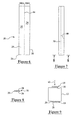
- Figures 6 and 7 are views of an electrode constructed in accordance with an alternative exemplary embodiment of the present invention;
- Figure 8 is a view along lines 8-8 of Figure 7;
- Figure 9 is an end view of a piezoelectric actuator with a pair of electrodes constructed in accordance with the alternative exemplary embodiment of Figures 6-8;
- Figures 10 and 11 are views of an electrode constructed in accordance with another alternative exemplary embodiment of the present invention;
- Figure 12 is a view along lines 12-12 of Figure 11;
- Figure 13 is an end view of a piezoelectric actuator with a pair of electrodes constructed in accordance with the alternative exemplary embodiment of Figures 10-12;
- Figures 14 and 15 are views of an electrode constructed in accordance with another alternative exemplary embodiment of the present invention;
- Figure 16 is a view along lines 16-16 of Figure 15;
- Figure 17 is an end view of a piezoelectric actuator with a pair of electrodes constructed in accordance with the alternative exemplary embodiment of Figures 14-16;
- Figures 18-22 are views illustrating another alternative exemplary embodiment of the present invention; and
- Figures 23-26 are view illustrating still another alternative exemplary embodiment of the present invention.
- Referring now to Figure 1 a multi-layer
piezoelectric actuator 10 constructed in accordance with an exemplary embodiment of the present invention is illustrated.Piezoelectric actuator 10 comprises astack 12 of sintered films of piezoceramic material or layers 14. Disposed therebetween are a plurality of insertedinternal metal electrodes 16 each having leads extending out of the stack in alternate directions and are electrically connected in parallel to a pair ofexternal electrodes 18. Although illustrated as having a rectangular configuration exemplary embodiments of the present invention are contemplated for use with a variety of actuator shapes (e.g., circular, square, triangular etc.), which may ultimately depend on the environment the actuators are used in. A non-limiting example of a piezoelectric stack and/or application thereof is found inU.S. patent numbers 6,464,149 and6,940,213 , the contents each of which are incorporated herein by reference thereto. -
Electrical conductors 20 are electrically terminated with the external electrodes. The electrical termination is provided by any suitable process, non-limiting examples include soldering, welding, etc. Upon the application of a voltage to the electrode, the stack expands in the direction of thearrows 22. If an alternating voltage of corresponding output is applied, the stack performs an expansion and contraction movement as dictated by the change in voltage. - After repeated expansion and contraction of the piezoelectric actuator, slight cracks will eventually occur in the ceramic material of the layers of the piezoelectric actuator. As discussed above, these cracks will pose problems, as they can also extend through the electrode fixedly secured to the side of the stack at the location where the crack surfaces. Therefore, some of the leads of the internal electrodes may no longer be supplied with a voltage as the termination with the electrode has been severed.
- In accordance with an exemplary embodiment of the present invention a strain tolerant electrode is provided. The strain tolerant electrode of exemplary embodiments of the present invention will address drawbacks found with wrought metal electrodes and cracks formed due to the expansion and contraction of the piezoelectric actuator.
- In accordance with exemplary embodiments of the present invention a layered electrode design is provided wherein a portion of a first portion or lower layer of the electrode is directly secured to the leads of the internal metal electrodes and the portion of the first portion or lower layer is allowed to crack during actuation of the piezoelectric stack. However, the electrical contact of each fractured segment on the stack is maintained through compliant connections with and/or a sliding contact with an intact common top electrode layer. In accordance with an exemplary embodiment, the top layer will not be subject to the cyclic strain of the bottom layer and therefore the top layer will not crack when the lower layer breaks.
- Referring now to Figures 2-5, an exemplary embodiment of a strain tolerant electrode is illustrated. Here electrode 18 comprises a sheet of electrically conductive metal 24 (e.g., steel, copper, nickel, invar, alloys, etc. including clad combinations of same and equivalents thereof) wherein
sheet 24 is folded upon itself to define alower layer 26 and anupper layer 28. In one non-limiting example, the electrode is comprised of two layers formed by folding the metal sheet. In one non-limiting exemplary embodiment, the metal sheet is approximately 0.002 inches (approximately 50 micrometres) thick. In accordance with an exemplary embodiment,lower layer 26 is electrically terminated to the leads of the internal electrodes via a bonding process whereinlower layer 26 is secured thereto. In addition,sheet 24 is cut to have a plurality of openings orstrain relief slots 29 to define a plurality ofcompliant members 30 when upper layer is folded upon the lower layer. - In one non-limiting exemplary embodiment the plurality of slots are formed in the sheet of conductive material by an electrical discharge machining process (EDM). Of course, any other suitable manufacturing process may be used to form the plurality of slots other non-limiting examples include, piercing, stamping, cutting, etc. and equivalents thereof.
- In accordance with one exemplary embodiment, the openings defining
compliant members 30 may be cut after the folding process, wherein the openings are cut into the folded longitudinal edge and extend inward about 2/3rds of the total electrode width. It should be appreciated that lengths greater or less than 2/3rds of the electrode width are contemplated to be within the scope of exemplary embodiments of the present invention. The cutting/forming of the compliant connections ormembers 30 can be done before or after the metal is folded to form the double thickness strip. - Accordingly, when in the folded configuration illustrated in Figures 3-5 the upper layer is in electrical contact with the lower layer via the compliant members as well as by interfacial contact between the
uncut surface 32 ofupper layer 28 making contact with a seconduncut surface 34 oflower layer 26. - As illustrated in Figure 5, the lower layer of the metal side electrode is soldered or bonded to the metalized thick film area of the stack with as much bond strength as possible since exemplary embodiments will mitigate the deleterious effects of cracks caused by strong bonds between the lower layer and the stack. Figure 5 illustrates a
bonding material 38 disposed between the lower layer and the leads of the internal electrodes. A non-limiting example of the method used forbonding layer 38 is soldering, brazing, welding or the use of a conductive epoxy. - As illustrated, the bottom layer is bonded to the stack of the metalized thick film area. As shown in Figures 2 and 5A, during repeated actuation of the device, a
crack 40 will only travel throughbottom layer 26. However, and in accordance with an exemplary embodiment, thetop layer 28 in Figures 4 and 5A will not crack because it is only connected to the lower layer via the highly compliant metal segments orcompliant members 30. Freedom of movement of the upper layer with respect to the lower layer is also provided, as there is no direct bonding betweensurface compliant members 30 are not bonded to the stack. Accordingly, any crack in the bottom layer will be electrically bridged by the top layer which is mechanically/electrically connected to it through the compliant segments as well as whensurface 32 is making contact withsurface 34. This design or embodiment of Figures 2-5 is appropriate for aside electrode 18 that will not experience significant normal compressive loads in the direction ofarrow 42 on the freely movingupper surface 28 and thecompliant members 30. An example of environments providing forces in the direction ofarrow 42 would be usage of the actuator in a vessel comprising high hydrostatic pressures. Figures 6-17 and 23-26 illustrate designs contemplated for use in environments wherein hydrostatic pressures or normal compressive loads are provided in the direction ofarrow 42 on the freely moving upper surface. - Referring now to Figures 6-9, another alternative exemplary embodiment of the present invention is illustrated. Here electrode 18 is formed by folding the sheet of electrically
conductive material 24 upon itself along aline 44 to create anupper layer 28 and alower layer 26 and a singlecompliant member 30 is provided. Singlecompliant member 30 traverses the entire length of the electrode, wherein thelower layer 26 and not thecompliant member 30 is bonded to the actuator. With cyclic strain a resultingcrack 40 will pass throughlayer 26 and extend intosection 30, creating multiple compliant metal electrical connections that maintain electrical communication between the cracked segments inlayers 26 and the un-crackedtop layer 28. Freedom of movement for the upper layer with respect to the lower layer is also provided as there is no direct bonding betweensurface surface layer 26. - In accordance with an exemplary embodiment, this design is suitable for use in environments when normal compressive loads are present on the upper layer in the direction of
arrow 42 during application of straintolerant electrode 18. - Referring now to Figures 10-13, another alternative exemplary embodiment of the present invention is illustrated. Here electrode 18 is formed by folding the sheet of electrically
conductive material 24 upon itself alongline 44 to create anupper layer 28 and alower layer 26, wherein the lower layer is bonded to the actuator. As in the previous embodiments, any resulting crack 40 (illustrated in Figure 10 via dashed lines) will pass throughlayer 26 while electrical connection remains across the leads of the internal electrode as compliant sections 30 (which can crack and maintain continuity) andsurface layer - In accordance with this embodiment, the upper and lower layers are connected to each other via
segments 30 formed by slots oropenings 29 cut into the sheet of electrode material in the longitudinal direction. In this embodiment, the slots or openings have a longer length alongline 44 as opposed to the openings of the embodiment illustrated in Figures 2-5. As in the previous embodiments only one side of thebottom strip 26 is bonded to stack and thetop strip 28 is relatively free and pressed against the bonded strip. Accordingly, the top strip can physically and electrically bridge any cracking in the bottom layer or strip because of interfacial contact pressure between the two layers (e.g., surfaces 32 and 34). During operation, the bottom layer will move with the stack during actuation, while the top layer will experience less motion. In addition, friction at the interface betweensurfaces - In yet another alternative exemplary embodiment, the folded common electrode could be formed from a flat strip with a
continuous slot 29 cut in the middle of the sheet of the electrode material. This is illustrated by the dashed lines in Figure 10 in this embodiment, the strip would be folded at the slot with a pair of tabs or compliant members disposed at the ends of the electrode and the slot in order to keep the strip layers in location for bonding of the lower layer. This design is also more tolerant for compressive loads applied to the upper layer of the electrode in the direction ofarrow 42. - Referring now to Figures 14-17, yet another alternative exemplary embodiment of the present invention is illustrated. Here electrode 18 is formed by folding the sheet of electrically
conductive material 24 upon itself alongline 44 to create anupper layer 28 and alower layer 26, whereinline 44 traverses the shorter width of the electrically conductive surface. Again, and as in the previous embodiments, the lower layer is bonded to the actuator and any resultingcrack 40 will pass only throughlayer 26 while electrical connection remains across thesurfaces layers layer - Even with multiple cracks in the bottom layer electrical contact will be maintained at the sliding interface between the two layers. In this embodiment, attachment between the layers would only be at the end of the electrode with the least amount of exposure to stress and strain. Moreover, the same location may be used for the terminal connection to the electrode. This design is particularly suitable for extreme compressive loads on the side electrode (e.g., loads in the direction of arrow 42).
- Referring now to Figures 18-22, another alternative exemplary embodiment of the present invention is illustrated. Here the
electrode 18 is configured to have a plurality ofcompliant members 30 disposed along the exterior edges of the upper and lower layers and the upper and lower layers are each configured to have a centrally locatedstrip relief slots 29 in the exterior edges of the electrically conductive metal. Thereafter, the cylinder is flattened out and the width of the compliant members is extended asupper layer 28 is pushed towardslower layer 26. As in the previous embodiments, only the lower layer is bonded to the stack while the upper layer is free to move with respect to the lower layer and the plurality of compliant members provide a conductive path between the upper and lower layers. It should be appreciated at this point that although a cylindrical shape is preferred, other shapes, such as rectangular and oval, are contemplated. - In addition, and in accordance with an exemplary embodiment the compliant members are configured to have an alternating arrangement with respect to each other. Accordingly, staggered compliant members are provided on both sides of the upper and lower solid strip electrodes and the metalized surface on the stack that is bonded to the piezoelectric stack, is centered as opposed to the off-center placement illustrated in Figures 2-5. In addition, the bonding of this side electrode to the internal electrodes in the stack is also limited to the bottom strip, wherein cracking and segmentation of the electrode is expected. The increased number and staggered placement of the compliant members, decreases the probability that multiple transverse cracks in the lower electrode strip could electrically isolate a compliant member from a particular lower electrode segment. The compliant members also physically and electrically bridge the cracked segments of the bottom electrode to the upper strip. The top electrode strip acts as an electrical buss that is decoupled by the compliant members from the cyclic strain caused during actuation of the piezoelectric stack.
- Referring now to Figures 23-26, another alternative exemplary embodiment of the present invention is illustrated. Here the
electrode 18 is configured to have a larger lower layer with a "U" shaped opening orchannel 80 disposed therein.Upper layer 28 is configured to have a smaller width than that oflower layer 26 andupper layer 28 is configured to be received within opening 80 asupper layer 28 is folded over and intolower layer 26. "U" shaped opening orchannel 80 will also have a pair ofsidewalls 82 extending along the length ofopening 80. - In this embodiment, the sidewalls will guide and maintain alignment of the top electrode strip movement (e.g., layer 28) with the bottom electrode (e.g., layer 26) during actuation of the piezoelectric stack. The top electrode strip acts as a stationary buss and the bottom electrode strip moves with the stack and can crack transversely as a result. This design is particularly suitable for extreme compressive loads on the side electrode (e.g., loads in the direction of arrow 42).
- An additional advantage of this arrangement is that the electrodes are self-aligning during assembly (e.g., folding over of
layer 28 into opening 80) and actuation (e.g., cyclical movement oflayer 26 but not layer 28). Moreover, full electrical contact betweenupper layer 28 andlower layer 26 is maintained during the lifetime of the stack, this is provided by the three surfaces (bottom and side walls) of U shapedopening 80. This will provide some additional advantage to the durability of the piezoelectric stack itself, in that stack cracking can promote stack misalignment with eventual failure of internal electrodes that are not capable of allowing for the cyclical strain. - While the invention has been described with reference to exemplary embodiments, it will be understood by those skilled in the art that various changes may be made and equivalents may be substituted for elements thereof without departing from the scope of the invention as defined by the claims. In addition, many modifications may be made to adapt a particular situation or material to the teachings of the invention without departing from the essential scope thereof. Therefore, it is intended that the invention not be limited to the particular embodiment disclosed as the best mode contemplated for carrying out this invention, but that the invention will include all embodiments falling within the scope of the present application.
- The invention is now exemplified by a series of clauses that recite various aspects and preferred embodiments.
- In a first aspect, the invention provides a strain tolerant electrode, comprising an upper layer a lower layer a plurality of transverse compliant members providing electrical communication between the upper layer and the lower layer and wherein a surface of the upper layer is in direct contact with a surface of the lower layer to provide an electrical path between the upper layer and the lower layer. As a result actuator expansion and contraction of the lower layer is possible without resulting expansion and contraction of the upper layer.
- Preferably the strain tolerant electrode is formed by cutting a plurality of openings in a sheet of conductive material and folding the sheet of conductive material so that a first portion of the plurality of openings overlies a second portion of the plurality of openings such that the upper layer and the lower layer are defined by portions of the conductive material disposed about opposite sides of the plurality of openings.
- Preferably, the plurality of compliant members are defined by the plurality of openings.
- In one embodiment, the strain tolerant electrode may be formed from a sheet of conductive material and the plurality of compliant members are defined by a plurality of openings along a center line of the sheet of conductive material, wherein the plurality of openings are spaced apart from each other along the center line wherein a portion of each of the plurality of openings is located on one side of the center line and another portion of each of the plurality of openings is located on the other side of the center line.
- In another embodiment, the upper layer and the lower layer may be defined by portions of the conductive material stacked to one side of the plurality of longitudinal openings, wherein the plurality of compliant members are defined by the plurality of openings.
- In another embodiment, the strain tolerant electrode may be formed by cutting a plurality of openings in a sheet of conductive material, wherein the sheet of conductive material is rectangular in shape and the plurality of openings are substantially parallel to a width of the sheet of conductive material. In this embodiment it is preferred that the width of the sheet of conductive material is substantially shorter than a length of the sheet of the conductive material.
- In another aspect the invention provides a strain tolerant electrode comprising an upper layer, a lower layer, a single compliant member at one end providing electrical communication between the upper layer and the lower layer, and wherein a surface of the upper layer is in direct contact with a surface of the lower layer to provide an electrical path between the upper layer and the lower layer.
- In another aspect the invention provides a piezoelectric actuator comprising a stack of piezoceramic layers, a plurality of internal metal electrodes, each having a lead extending out of the stack of piezoceramic layers in alternate directions on opposite sides of the stack of piezoceramic layers, a first external electrode electrically connected to the leads of the internal metal electrodes extending out of one side of the stack of piezoceramic layers, a second external electrode electrically connected to the leads of the internal metal electrodes extending out of another side of the stack of piezoceramic layers, wherein the first external electrode and the second external electrode each comprise an upper layer, a lower layer, a plurality of transverse compliant members providing electrical communication between the upper layer and the lower layer; and wherein a surface of the upper layer is in direct contact with a surface of the lower layer to provide an electrical path between the upper layer and the lower layer. As a result of this configuration expansion and contraction of the lower layer is possible without resulting expansion and contraction of the upper layer.
- Preferably, the first and second external electrodes may be formed by cutting a plurality of openings in a sheet of conductive material and folding the sheet of conductive material so that a first portion of the plurality of openings overlies a second portion of the plurality of openings, and wherein the upper layer and the lower layer of the first and second external electrodes are defined by portions of the conductive material disposed about opposite sides of the plurality of openings.
- Preferably, the plurality of compliant members of the first and second external electrodes may be defined by the plurality of openings.
- In one embodiment, the first and second external electrodes may be formed from a sheet of conductive material and the plurality of compliant members may be defined by a plurality of openings along a center line of the sheet of conductive material, wherein the plurality of openings are spaced apart from each other along the center line wherein a portion of each of the plurality of openings is located on one side of the center line and another portion of each of the plurality of openings is located on the other side of the center line.
- In this embodiment, preferably the upper layer and the lower layer of the first and second external electrodes are defined by portions of the sheet of conductive material stacked to one side of the plurality of openings, wherein the plurality of compliant members may be defined by the plurality of openings.
- Preferably, the first and second external electrodes may be connected at one end of the electrode and the electrode has a rectangular shape. Also, in this embodiment it is preferred that the width of the sheet of conductive material is substantially shorter than a length of the sheet of the conductive material.
- In another aspect the invention provides a method for manufacturing a strain tolerant electrode, the method comprising cutting a plurality of slots within a sheet of conductive material, folding the sheet of conductive material upon itself to define an upper layer and a lower layer, wherein the plurality of slots define a plurality of compliant members each of which providing electrical communication between the upper layer and the lower layer and wherein a surface of the upper layer is in direct contact with a surface of the lower layer after the sheet of conductive material is folded upon itself, wherein any cracks in the lower layer are bridged by the plurality of compliant members and/or the direct contact between the surface of the lower layer and the surface of the upper layer. As a result of the above manufactured electrode, expansion and contraction of the lower layer is possible without resulting expansion and contraction of the upper layer. Therefore, movement between of the upper and lower layers is substantially independent.
- In one embodiment, preferably the sheet of conductive material is folded such that a first portion of the plurality of slots overlies a second portion of the plurality of slots and the upper layer and the lower layer are defined by portions of the sheet of conductive material disposed about opposite sides of the plurality of slots.
- In another embodiment, conductive sheet is formed such that the plurality of slots are located along a center line of the sheet of conductive material, wherein the plurality of slots are spaced apart from each other along the center line wherein a portion of each of the plurality of slots is located on one side of the center line and another portion of each of the plurality of slots is located on the other side of the center line.
- In another aspect, the invention provides a strain tolerant electrode, comprising an upper layer, a lower layer, a plurality of transverse compliant members providing electrical communication between the upper layer and the lower layer through an electrical path between the upper layer and the lower layer, wherein the electrical path is only proved by the plurality of transverse compliant members.
- In another aspect, the invention provides a strain tolerant electrode comprising an upper layer, a lower layer, a single compliant member providing electrical communication between the upper layer and the lower layer; and a plurality of transverse compliant members formed from the single compliant member, the plurality of transverse compliant members being formed during a segmentation of the single compliant member wherein the segmentation of the single compliant member occurs during cyclical expansion and contraction of the single compliant member and the plurality of plurality of transverse compliant members provide electrical communication between the upper layer and the lower layer, and wherein a surface of the upper layer is in direct contact with a surface of the lower layer to provide an electrical path between the upper layer and the lower layer.
- In another aspect the invention provides a piezoelectric actuator comprising a stack of piezoceramic layers, a plurality of internal metal electrodes, each having a lead extending out of the stack of piezoceramic layers in alternate directions on opposite sides of the stack of piezoceramic layers, a first external electrode electrically connected to the leads of the internal metal electrodes extending out of one side of the stack of piezoceramic layers, a second external electrode electrically connected to the leads of the internal metal electrodes extending out of another side of the stack of piezoceramic layers, wherein the first external electrode and the second external electrode each comprise an upper layer, a lower layer, a plurality of transverse compliant members providing electrical communication between the upper layer and the lower layer through an electrical path between the upper layer and the lower layer, wherein the electrical path is only provided by the plurality of transverse compliant members.
- In another aspect the invention provides a piezoelectric actuator comprising a stack of piezoceramic layers a plurality of internal metal electrodes, each having a lead extending out of the stack of piezoceramic layers sequentially in alternate directions on opposite sides of the stack of piezoceramic layers, a first external electrode electrically connected to the leads of the internal metal electrodes extending out of one side of the stack of piezoceramic layers, a second external electrode electrically connected to the leads of the internal metal electrodes extending out of another side of the stack of piezoceramic layers, wherein the first external electrode and the second external electrode each comprise, an upper layer, a lower layer, a single compliant member providing electrical communication between the upper layer and the lower layer, and a plurality of transverse compliant members formed from the single compliant member, the plurality of transverse compliant members being formed during a segmentation of the single compliant member wherein the segmentation of the single compliant member occurs during cyclical expansion and contraction of the single compliant member and the plurality of plurality of transverse compliant members provide electrical communication between the upper layer and the lower layer, and wherein a surface of the upper layer is in direct contact with a surface of the lower layer to provide an electrical path between the upper layer and the lower layer.
Claims (27)
- A strain tolerant electrode (18), particularly for use with a piezoelectric stack-type actuator, comprising an upper layer (28), a lower layer (26) and one or more compliant members (30) providing electrical connection between the upper layer (28) and the lower layer (26).
- The electrode of claim 1, wherein the electrode (18) comprises a sheet of conductive material folded such that the upper layer (28) lies adjacent the lower layer (26).
- The electrode of claim 2, wherein a surface of the upper layer (28) contacts a surface of the lower layer (26) to provide an electrical path therebetween.
- The electrode of claim 3, wherein the contact between the surface of the upper layer (28) and the lower layer (26) is such as to allow one layer to slide with respect to the other layer.
- The electrode of claim 4, wherein a lubricant is disposed between the respective surfaces of the upper layer (28) and the lower layer (26).
- The electrode of any one of claims 1 to 5, wherein the or each compliant member (30) is segmented, in use, to form a plurality of transverse compliant members (30) that provide an electrical path between the upper layer (28) and lower layer (26).
- The electrode of any one of claims 1 to 5, wherein the electrode (18) is shaped to define a longitudinal edge and a transverse edge, and wherein a single compliant member (30) is defined at the longitudinal edge.
- The electrode of any one of claims 2 to 5, wherein an opening (29) is disposed along a centre line of the sheet of conductive material so as to define first and second compliant members, a portion of the opening (29) being located on one side of the centre line and another portion of the opening being located on the other side of the centre line.
- The electrode of any one of claims 1 to 5, wherein the electrode (18) is shaped to define a longitudinal edge and a transverse edge, and wherein a single compliant member (30) is defined at the transverse edge.
- The electrode of claim 9, wherein the lower layer (26) is U-shaped in cross section so as to define a channel (80) for receiving the upper layer (28).
- The electrode of any one of claims 1 to 5, including a plurality of compliant members (30).
- The electrode of claim 11, wherein the plurality of compliant members (30) are defined by a plurality of openings (29).
- The electrode of claim 12, wherein the plurality of openings (29) are disposed along a centre line (44) of the sheet of conductive material, wherein the plurality of openings (29) are spaced apart from each other along the centre line (44), a portion of each of the plurality of openings (29) being located on one side of the centre line (44) and another portion of each of the plurality of openings (29) is located on the other side of the centre line (29).
- The electrode of claim 12, wherein a first portion of the plurality of openings (29) overlies a second portion of the plurality of openings (29).
- The electrode of any one of claims 10 to 14, wherein the upper layer (28) and the lower layer (26) are defined by portions of the electrode (18) disposed about opposite sides of the plurality of openings (29).
- The electrode of any one of claims 10 to 14, wherein the upper layer (28) and the lower layer (26) are defined by portions of the conductive material stacked to one side of the plurality of openings (29).
- The electrode of claim 12, wherein the upper layer (28) and the lower layer (26) are disposed longitudinally, one above the other, approximately along the centre line (44) of the electrode (28), and flanked by the plurality of openings (29).
- A piezoelectric actuator comprising a stack of piezoceramic layers and internal electrodes and carrying at least one external electrode as claimed in any one of claims 1 to 17.
- A method of manufacturing a strain tolerant electrode comprising providing a sheet of conductive material and folding the sheet of conductive material upon itself to define an upper layer (28) and a lower layer (26) and a compliant member (30) providing an electrical path therebetween.
- The method of claim 19, including arranging the upper layer (28) and the lower layer (26) such that a respective surface (32, 34) thereof lie against each other in direct contact.
- The method of claim 20, including applying a lubricant to one or each of the surfaces (32, 34) of the upper layer (28) and the lower layer (26).
- The method of any one of claims 19 to 21, including forming one or more openings (29) in the sheet of conductive material so as to define a plurality of compliant members (30).
- The method of claim 22, wherein the or each opening (29) is formed along a centre line (44) of the sheet of conductive material, wherein a portion of the or each opening (29) is located on one side of the centre line and another portion of the or each opening (29) is located on the other side of the centre line.
- The method of claim 22, wherein the or each opening (29) is formed substantially parallel to a transverse edge of the sheet of conductive material.
- The method of claim 24, including folding the sheet of conductive material so as to arrange a first portion of the or each opening (29) to overlay a second portion of the or each opening (29).
- The method of any on of claims 19 to 25, including forming a plurality of compliant members (30) from a single compliant member during use of the electrode (18).
- The method of any one of claims 19 to 25, wherein the folding step includes forming the sheet of conductive material into substantially a cylindrical shape prior to forming the plurality of openings.
Applications Claiming Priority (1)
| Application Number | Priority Date | Filing Date | Title |
|---|---|---|---|
| US11/496,189 US7679273B2 (en) | 2006-07-31 | 2006-07-31 | Strain tolerant metal electrode design |
Publications (3)
| Publication Number | Publication Date |
|---|---|
| EP1885005A2 true EP1885005A2 (en) | 2008-02-06 |
| EP1885005A3 EP1885005A3 (en) | 2009-05-20 |
| EP1885005B1 EP1885005B1 (en) | 2011-02-23 |
Family
ID=38616362
Family Applications (1)
| Application Number | Title | Priority Date | Filing Date |
|---|---|---|---|
| EP07252923A Not-in-force EP1885005B1 (en) | 2006-07-31 | 2007-07-24 | An electrode for a piezoelectric actuator |
Country Status (5)
| Country | Link |
|---|---|
| US (1) | US7679273B2 (en) |
| EP (1) | EP1885005B1 (en) |
| JP (1) | JP2008034855A (en) |
| AT (1) | ATE499710T1 (en) |
| DE (1) | DE602007012622D1 (en) |
Families Citing this family (3)
| Publication number | Priority date | Publication date | Assignee | Title |
|---|---|---|---|---|
| JP4775372B2 (en) * | 2005-02-15 | 2011-09-21 | 株式会社村田製作所 | Multilayer piezoelectric element |
| WO2009125553A1 (en) * | 2008-04-11 | 2009-10-15 | 株式会社村田製作所 | Laminated piezoelectric actuator |
| DE102008062021A1 (en) * | 2008-08-18 | 2010-03-04 | Epcos Ag | Piezo actuator in multilayer construction |
Family Cites Families (22)
| Publication number | Priority date | Publication date | Assignee | Title |
|---|---|---|---|---|
| JPH04340778A (en) * | 1991-01-30 | 1992-11-27 | Nec Corp | Laminated piezoelectric actuator element |
| JP3087369B2 (en) * | 1991-09-09 | 2000-09-11 | トヨタ自動車株式会社 | Piezoelectric laminate |
| DE19648545B4 (en) | 1996-11-25 | 2009-05-07 | Ceramtec Ag | Monolithic multilayer actuator with external electrodes |
| DE19930585B4 (en) | 1998-08-06 | 2017-11-09 | Epcos Ag | Piezoelectric actuator with improved electrical contacting and use of such a piezoelectric actuator |
| DE19856185A1 (en) | 1998-12-05 | 2000-06-15 | Bosch Gmbh Robert | Piezoelectric drive |
| EP1061591A4 (en) | 1998-12-18 | 2007-05-02 | Denso Corp | PIEZOELECTRIC MULTILAYER BODY |
| DE19909482A1 (en) * | 1999-03-04 | 2000-09-07 | Bosch Gmbh Robert | Piezoelectric actuator |
| DE19917728A1 (en) * | 1999-04-20 | 2000-10-26 | Bosch Gmbh Robert | Piezoelectric actuator particularly for operating control valves or injection valves in vehicles, has additional planar electrode strip adjacent actuator body with double comb-type legs |
| DE19928190A1 (en) * | 1999-06-19 | 2001-01-11 | Bosch Gmbh Robert | Piezo actuator |
| DE19928189A1 (en) * | 1999-06-19 | 2001-04-19 | Bosch Gmbh Robert | Piezo actuator |
| GB9925410D0 (en) * | 1999-10-28 | 1999-12-29 | Lucus Ind Plc | Actuator arrangement |
| JP2002203999A (en) | 2000-11-06 | 2002-07-19 | Denso Corp | Laminated piezoelectric element and method of manufacturing the same |
| JP4248777B2 (en) * | 2000-12-28 | 2009-04-02 | 株式会社デンソー | Piezoelectric element for injector, method for manufacturing the same, and injector |
| JP3964184B2 (en) * | 2000-12-28 | 2007-08-22 | 株式会社デンソー | Multilayer piezoelectric actuator |
| US6700306B2 (en) | 2001-02-27 | 2004-03-02 | Kyocera Corporation | Laminated piezo-electric device |
| DE10234787C1 (en) * | 2002-06-07 | 2003-10-30 | Pi Ceramic Gmbh Keramische Tec | Manufacturing method for monolithic multi-layer piezoceramic actuator with microfaults provided in actuator joints parallel to inner electrodes |
| DE10327902A1 (en) * | 2002-07-19 | 2004-06-24 | Ceramtec Ag Innovative Ceramic Engineering | External electrode on a piezoceramic multilayer actuator |
| DE102004002484A1 (en) * | 2004-01-17 | 2005-08-11 | Robert Bosch Gmbh | Piezoelectric actuator for an internal combustion engine injection valve has an actuator body to expand and contract when operating the piezoelectric actuator |
| DE102004004737A1 (en) * | 2004-01-30 | 2005-08-18 | Robert Bosch Gmbh | Piezoactuator and a method for its production |
| US7385337B2 (en) * | 2004-06-18 | 2008-06-10 | Tdk Corporation | Multilayer piezoelectric element |
| JP2006303044A (en) * | 2005-04-18 | 2006-11-02 | Denso Corp | Multilayer piezoelectric element |
| JP4929875B2 (en) * | 2006-06-30 | 2012-05-09 | 株式会社デンソー | Multilayer piezoelectric element |
-
2006
- 2006-07-31 US US11/496,189 patent/US7679273B2/en not_active Expired - Fee Related
-
2007
- 2007-07-24 AT AT07252923T patent/ATE499710T1/en not_active IP Right Cessation
- 2007-07-24 DE DE602007012622T patent/DE602007012622D1/en active Active
- 2007-07-24 EP EP07252923A patent/EP1885005B1/en not_active Not-in-force
- 2007-07-31 JP JP2007198268A patent/JP2008034855A/en active Pending
Non-Patent Citations (1)
| Title |
|---|
| None |
Also Published As
| Publication number | Publication date |
|---|---|
| JP2008034855A (en) | 2008-02-14 |
| EP1885005B1 (en) | 2011-02-23 |
| ATE499710T1 (en) | 2011-03-15 |
| US20080024043A1 (en) | 2008-01-31 |
| DE602007012622D1 (en) | 2011-04-07 |
| US7679273B2 (en) | 2010-03-16 |
| EP1885005A3 (en) | 2009-05-20 |
Similar Documents
| Publication | Publication Date | Title |
|---|---|---|
| US8638025B2 (en) | Piezo actuator with external electrode soldered to outer face | |
| CZ2001576A3 (en) | Piezoelectric controller | |
| US20090000597A1 (en) | Piezoceramic Multilayer Actuator, Method for Producing a Piezoceramic Multilayer Actuator, and Inujection System | |
| JP4843143B2 (en) | Piezoelectric actuator | |
| EP1162671B1 (en) | Piezoelectric device for injector | |
| EP1885005B1 (en) | An electrode for a piezoelectric actuator | |
| CZ2001578A3 (en) | Piezoelectric controller | |
| US6528927B1 (en) | Piezo actuator with multi-layer conductive film, and method for making same | |
| US6414418B1 (en) | Piezoelectric actuator | |
| WO2009064990A1 (en) | Planar spring assembly with attached solder strip | |
| US9130152B2 (en) | Piezoelectric component | |
| US8304963B2 (en) | Piezoactuator with a predetermined breaking layer | |
| TW543160B (en) | Re-contacting for an electrical component as well as piezoelectrical component in several-layers construction | |
| US7259504B2 (en) | Piezoelectric actuator | |
| KR20010072858A (en) | Piezo-multilayer actuator with improved electrode contact | |
| US9214620B2 (en) | Piezoelectric actuator with outer electrode | |
| US5155409A (en) | Integral conductor for a piezoelectric actuator | |
| WO2009130863A1 (en) | Multilayer piezoelectric actuator | |
| US7015629B2 (en) | Additional contacting for an electrical component and piezoelectric component in the form of a multilayer structure | |
| WO2009125553A1 (en) | Laminated piezoelectric actuator | |
| CN1473365A (en) | piezoelectric actuator | |
| JP5687935B2 (en) | Piezoelectric actuator | |
| EP2224123A1 (en) | Piezoelectric actuator | |
| EP1650816A1 (en) | Piezoelectric actuator | |
| JPH09270539A (en) | Laminated piezoelectric actuator |
Legal Events
| Date | Code | Title | Description |
|---|---|---|---|
| PUAI | Public reference made under article 153(3) epc to a published international application that has entered the european phase |
Free format text: ORIGINAL CODE: 0009012 |
|
| AK | Designated contracting states |
Kind code of ref document: A2 Designated state(s): AT BE BG CH CY CZ DE DK EE ES FI FR GB GR HU IE IS IT LI LT LU LV MC MT NL PL PT RO SE SI SK TR |
|
| AX | Request for extension of the european patent |
Extension state: AL BA HR MK YU |
|
| PUAL | Search report despatched |
Free format text: ORIGINAL CODE: 0009013 |
|
| AK | Designated contracting states |
Kind code of ref document: A3 Designated state(s): AT BE BG CH CY CZ DE DK EE ES FI FR GB GR HU IE IS IT LI LT LU LV MC MT NL PL PT RO SE SI SK TR |
|
| AX | Request for extension of the european patent |
Extension state: AL BA HR MK RS |
|
| 17P | Request for examination filed |
Effective date: 20091106 |
|
| 17Q | First examination report despatched |
Effective date: 20091127 |
|
| AKX | Designation fees paid |
Designated state(s): AT BE BG CH CY CZ DE DK EE ES FI FR GB GR HU IE IS IT LI LT LU LV MC MT NL PL PT RO SE SI SK TR |
|
| RAP1 | Party data changed (applicant data changed or rights of an application transferred) |
Owner name: DELPHI TECHNOLOGIES HOLDING S.A.R.L. |
|
| GRAP | Despatch of communication of intention to grant a patent |
Free format text: ORIGINAL CODE: EPIDOSNIGR1 |
|
| GRAS | Grant fee paid |
Free format text: ORIGINAL CODE: EPIDOSNIGR3 |
|
| GRAA | (expected) grant |
Free format text: ORIGINAL CODE: 0009210 |
|
| AK | Designated contracting states |
Kind code of ref document: B1 Designated state(s): AT BE BG CH CY CZ DE DK EE ES FI FR GB GR HU IE IS IT LI LT LU LV MC MT NL PL PT RO SE SI SK TR |
|
| REG | Reference to a national code |
Ref country code: GB Ref legal event code: FG4D |
|
| REG | Reference to a national code |
Ref country code: CH Ref legal event code: EP |
|
| REG | Reference to a national code |
Ref country code: IE Ref legal event code: FG4D |
|
| REF | Corresponds to: |
Ref document number: 602007012622 Country of ref document: DE Date of ref document: 20110407 Kind code of ref document: P |
|
| REG | Reference to a national code |
Ref country code: DE Ref legal event code: R096 Ref document number: 602007012622 Country of ref document: DE Effective date: 20110407 |
|
| REG | Reference to a national code |
Ref country code: NL Ref legal event code: VDEP Effective date: 20110223 |
|
| LTIE | Lt: invalidation of european patent or patent extension |
Effective date: 20110223 |
|
| PG25 | Lapsed in a contracting state [announced via postgrant information from national office to epo] |
Ref country code: GR Free format text: LAPSE BECAUSE OF FAILURE TO SUBMIT A TRANSLATION OF THE DESCRIPTION OR TO PAY THE FEE WITHIN THE PRESCRIBED TIME-LIMIT Effective date: 20110524 Ref country code: SE Free format text: LAPSE BECAUSE OF FAILURE TO SUBMIT A TRANSLATION OF THE DESCRIPTION OR TO PAY THE FEE WITHIN THE PRESCRIBED TIME-LIMIT Effective date: 20110223 Ref country code: LT Free format text: LAPSE BECAUSE OF FAILURE TO SUBMIT A TRANSLATION OF THE DESCRIPTION OR TO PAY THE FEE WITHIN THE PRESCRIBED TIME-LIMIT Effective date: 20110223 Ref country code: PT Free format text: LAPSE BECAUSE OF FAILURE TO SUBMIT A TRANSLATION OF THE DESCRIPTION OR TO PAY THE FEE WITHIN THE PRESCRIBED TIME-LIMIT Effective date: 20110623 Ref country code: ES Free format text: LAPSE BECAUSE OF FAILURE TO SUBMIT A TRANSLATION OF THE DESCRIPTION OR TO PAY THE FEE WITHIN THE PRESCRIBED TIME-LIMIT Effective date: 20110603 Ref country code: LV Free format text: LAPSE BECAUSE OF FAILURE TO SUBMIT A TRANSLATION OF THE DESCRIPTION OR TO PAY THE FEE WITHIN THE PRESCRIBED TIME-LIMIT Effective date: 20110223 |
|
| PG25 | Lapsed in a contracting state [announced via postgrant information from national office to epo] |
Ref country code: BE Free format text: LAPSE BECAUSE OF FAILURE TO SUBMIT A TRANSLATION OF THE DESCRIPTION OR TO PAY THE FEE WITHIN THE PRESCRIBED TIME-LIMIT Effective date: 20110223 Ref country code: CY Free format text: LAPSE BECAUSE OF FAILURE TO SUBMIT A TRANSLATION OF THE DESCRIPTION OR TO PAY THE FEE WITHIN THE PRESCRIBED TIME-LIMIT Effective date: 20110223 Ref country code: NL Free format text: LAPSE BECAUSE OF FAILURE TO SUBMIT A TRANSLATION OF THE DESCRIPTION OR TO PAY THE FEE WITHIN THE PRESCRIBED TIME-LIMIT Effective date: 20110223 Ref country code: AT Free format text: LAPSE BECAUSE OF FAILURE TO SUBMIT A TRANSLATION OF THE DESCRIPTION OR TO PAY THE FEE WITHIN THE PRESCRIBED TIME-LIMIT Effective date: 20110223 Ref country code: SI Free format text: LAPSE BECAUSE OF FAILURE TO SUBMIT A TRANSLATION OF THE DESCRIPTION OR TO PAY THE FEE WITHIN THE PRESCRIBED TIME-LIMIT Effective date: 20110223 Ref country code: FI Free format text: LAPSE BECAUSE OF FAILURE TO SUBMIT A TRANSLATION OF THE DESCRIPTION OR TO PAY THE FEE WITHIN THE PRESCRIBED TIME-LIMIT Effective date: 20110223 Ref country code: BG Free format text: LAPSE BECAUSE OF FAILURE TO SUBMIT A TRANSLATION OF THE DESCRIPTION OR TO PAY THE FEE WITHIN THE PRESCRIBED TIME-LIMIT Effective date: 20110523 |
|
| REG | Reference to a national code |
Ref country code: HU Ref legal event code: AG4A Ref document number: E011256 Country of ref document: HU |
|
| PG25 | Lapsed in a contracting state [announced via postgrant information from national office to epo] |
Ref country code: DK Free format text: LAPSE BECAUSE OF FAILURE TO SUBMIT A TRANSLATION OF THE DESCRIPTION OR TO PAY THE FEE WITHIN THE PRESCRIBED TIME-LIMIT Effective date: 20110223 Ref country code: EE Free format text: LAPSE BECAUSE OF FAILURE TO SUBMIT A TRANSLATION OF THE DESCRIPTION OR TO PAY THE FEE WITHIN THE PRESCRIBED TIME-LIMIT Effective date: 20110223 |
|
| PG25 | Lapsed in a contracting state [announced via postgrant information from national office to epo] |
Ref country code: CZ Free format text: LAPSE BECAUSE OF FAILURE TO SUBMIT A TRANSLATION OF THE DESCRIPTION OR TO PAY THE FEE WITHIN THE PRESCRIBED TIME-LIMIT Effective date: 20110223 Ref country code: SK Free format text: LAPSE BECAUSE OF FAILURE TO SUBMIT A TRANSLATION OF THE DESCRIPTION OR TO PAY THE FEE WITHIN THE PRESCRIBED TIME-LIMIT Effective date: 20110223 Ref country code: RO Free format text: LAPSE BECAUSE OF FAILURE TO SUBMIT A TRANSLATION OF THE DESCRIPTION OR TO PAY THE FEE WITHIN THE PRESCRIBED TIME-LIMIT Effective date: 20110223 |
|
| PG25 | Lapsed in a contracting state [announced via postgrant information from national office to epo] |
Ref country code: MT Free format text: LAPSE BECAUSE OF FAILURE TO SUBMIT A TRANSLATION OF THE DESCRIPTION OR TO PAY THE FEE WITHIN THE PRESCRIBED TIME-LIMIT Effective date: 20110223 |
|
| PLBE | No opposition filed within time limit |
Free format text: ORIGINAL CODE: 0009261 |
|
| STAA | Information on the status of an ep patent application or granted ep patent |
Free format text: STATUS: NO OPPOSITION FILED WITHIN TIME LIMIT |
|
| 26N | No opposition filed |
Effective date: 20111124 |
|
| PG25 | Lapsed in a contracting state [announced via postgrant information from national office to epo] |
Ref country code: MC Free format text: LAPSE BECAUSE OF NON-PAYMENT OF DUE FEES Effective date: 20110731 Ref country code: PL Free format text: LAPSE BECAUSE OF FAILURE TO SUBMIT A TRANSLATION OF THE DESCRIPTION OR TO PAY THE FEE WITHIN THE PRESCRIBED TIME-LIMIT Effective date: 20110223 |
|
| REG | Reference to a national code |
Ref country code: CH Ref legal event code: PL |
|
| REG | Reference to a national code |
Ref country code: DE Ref legal event code: R097 Ref document number: 602007012622 Country of ref document: DE Effective date: 20111124 |
|
| GBPC | Gb: european patent ceased through non-payment of renewal fee |
Effective date: 20110724 |
|
| REG | Reference to a national code |
Ref country code: IE Ref legal event code: MM4A |
|
| PG25 | Lapsed in a contracting state [announced via postgrant information from national office to epo] |
Ref country code: CH Free format text: LAPSE BECAUSE OF NON-PAYMENT OF DUE FEES Effective date: 20110731 Ref country code: LI Free format text: LAPSE BECAUSE OF NON-PAYMENT OF DUE FEES Effective date: 20110731 |
|
| PG25 | Lapsed in a contracting state [announced via postgrant information from national office to epo] |
Ref country code: IT Free format text: LAPSE BECAUSE OF FAILURE TO SUBMIT A TRANSLATION OF THE DESCRIPTION OR TO PAY THE FEE WITHIN THE PRESCRIBED TIME-LIMIT Effective date: 20110223 |
|
| PG25 | Lapsed in a contracting state [announced via postgrant information from national office to epo] |
Ref country code: GB Free format text: LAPSE BECAUSE OF NON-PAYMENT OF DUE FEES Effective date: 20110724 |
|
| PG25 | Lapsed in a contracting state [announced via postgrant information from national office to epo] |
Ref country code: IE Free format text: LAPSE BECAUSE OF NON-PAYMENT OF DUE FEES Effective date: 20110724 |
|
| PG25 | Lapsed in a contracting state [announced via postgrant information from national office to epo] |
Ref country code: LU Free format text: LAPSE BECAUSE OF NON-PAYMENT OF DUE FEES Effective date: 20110724 |
|
| PG25 | Lapsed in a contracting state [announced via postgrant information from national office to epo] |
Ref country code: IS Free format text: LAPSE BECAUSE OF FAILURE TO SUBMIT A TRANSLATION OF THE DESCRIPTION OR TO PAY THE FEE WITHIN THE PRESCRIBED TIME-LIMIT Effective date: 20110223 |
|
| REG | Reference to a national code |
Ref country code: FR Ref legal event code: TP Owner name: DELPHI INTERNATIONAL OPERATIONS LUXEMBOURG S.A, LU Effective date: 20140516 |
|
| REG | Reference to a national code |
Ref country code: DE Ref legal event code: R082 Ref document number: 602007012622 Country of ref document: DE Representative=s name: MANITZ, FINSTERWALD & PARTNER GBR, DE |
|
| REG | Reference to a national code |
Ref country code: HU Ref legal event code: GB9C Owner name: DELPHI INTERNATIONAL OPERATIONS LUXEMBOURG S.A, LU Free format text: FORMER OWNER(S): DELPHI TECHNOLOGIES HOLDING S.A.R.L., LU |
|
| REG | Reference to a national code |
Ref country code: DE Ref legal event code: R082 Ref document number: 602007012622 Country of ref document: DE Representative=s name: MANITZ FINSTERWALD PATENTANWAELTE PARTMBB, DE Effective date: 20140702 Ref country code: DE Ref legal event code: R081 Ref document number: 602007012622 Country of ref document: DE Owner name: DELPHI INTERNATIONAL OPERATIONS LUXEMBOURG S.A, LU Free format text: FORMER OWNER: DELPHI TECHNOLOGIES HOLDING S.A.R.L., BASCHARAGE, LU Effective date: 20140702 Ref country code: DE Ref legal event code: R082 Ref document number: 602007012622 Country of ref document: DE Representative=s name: MANITZ, FINSTERWALD & PARTNER GBR, DE Effective date: 20140702 |
|
| REG | Reference to a national code |
Ref country code: FR Ref legal event code: PLFP Year of fee payment: 9 |
|
| PGFP | Annual fee paid to national office [announced via postgrant information from national office to epo] |
Ref country code: DE Payment date: 20150729 Year of fee payment: 9 |
|
| PGFP | Annual fee paid to national office [announced via postgrant information from national office to epo] |
Ref country code: TR Payment date: 20150710 Year of fee payment: 9 Ref country code: HU Payment date: 20150715 Year of fee payment: 9 Ref country code: FR Payment date: 20150717 Year of fee payment: 9 |
|
| REG | Reference to a national code |
Ref country code: DE Ref legal event code: R119 Ref document number: 602007012622 Country of ref document: DE |
|
| PG25 | Lapsed in a contracting state [announced via postgrant information from national office to epo] |
Ref country code: DE Free format text: LAPSE BECAUSE OF NON-PAYMENT OF DUE FEES Effective date: 20170201 Ref country code: FR Free format text: LAPSE BECAUSE OF NON-PAYMENT OF DUE FEES Effective date: 20160801 Ref country code: HU Free format text: LAPSE BECAUSE OF NON-PAYMENT OF DUE FEES Effective date: 20160725 |
|
| REG | Reference to a national code |
Ref country code: FR Ref legal event code: ST Effective date: 20170331 |
|
| PG25 | Lapsed in a contracting state [announced via postgrant information from national office to epo] |
Ref country code: TR Free format text: LAPSE BECAUSE OF NON-PAYMENT OF DUE FEES Effective date: 20160724 |