EP1884963A1 - Multilayer directional coupler - Google Patents
Multilayer directional coupler Download PDFInfo
- Publication number
- EP1884963A1 EP1884963A1 EP06731042A EP06731042A EP1884963A1 EP 1884963 A1 EP1884963 A1 EP 1884963A1 EP 06731042 A EP06731042 A EP 06731042A EP 06731042 A EP06731042 A EP 06731042A EP 1884963 A1 EP1884963 A1 EP 1884963A1
- Authority
- EP
- European Patent Office
- Prior art keywords
- transformer
- directional coupler
- secondary coil
- ratio
- primary coil
- Prior art date
- Legal status (The legal status is an assumption and is not a legal conclusion. Google has not performed a legal analysis and makes no representation as to the accuracy of the status listed.)
- Withdrawn
Links
- 238000004804 winding Methods 0.000 claims abstract description 41
- 239000000758 substrate Substances 0.000 claims abstract description 18
- 230000008878 coupling Effects 0.000 abstract description 18
- 238000010168 coupling process Methods 0.000 abstract description 18
- 238000005859 coupling reaction Methods 0.000 abstract description 18
- 239000004020 conductor Substances 0.000 description 59
- 238000009826 distribution Methods 0.000 description 5
- 238000005516 engineering process Methods 0.000 description 4
- 238000000206 photolithography Methods 0.000 description 4
- 238000010586 diagram Methods 0.000 description 3
- 238000010030 laminating Methods 0.000 description 2
- 238000010295 mobile communication Methods 0.000 description 2
- 230000005540 biological transmission Effects 0.000 description 1
- 230000001413 cellular effect Effects 0.000 description 1
- 230000001419 dependent effect Effects 0.000 description 1
- 230000005283 ground state Effects 0.000 description 1
- 238000004519 manufacturing process Methods 0.000 description 1
- 239000000463 material Substances 0.000 description 1
- 238000000034 method Methods 0.000 description 1
- 238000004088 simulation Methods 0.000 description 1
- 238000005549 size reduction Methods 0.000 description 1
Images





Classifications
-
- H—ELECTRICITY
- H01—ELECTRIC ELEMENTS
- H01F—MAGNETS; INDUCTANCES; TRANSFORMERS; SELECTION OF MATERIALS FOR THEIR MAGNETIC PROPERTIES
- H01F37/00—Fixed inductances not covered by group H01F17/00
-
- H—ELECTRICITY
- H01—ELECTRIC ELEMENTS
- H01F—MAGNETS; INDUCTANCES; TRANSFORMERS; SELECTION OF MATERIALS FOR THEIR MAGNETIC PROPERTIES
- H01F17/00—Fixed inductances of the signal type
- H01F17/0006—Printed inductances
- H01F17/0013—Printed inductances with stacked layers
-
- H—ELECTRICITY
- H03—ELECTRONIC CIRCUITRY
- H03H—IMPEDANCE NETWORKS, e.g. RESONANT CIRCUITS; RESONATORS
- H03H7/00—Multiple-port networks comprising only passive electrical elements as network components
- H03H7/48—Networks for connecting several sources or loads, working on the same frequency or frequency band, to a common load or source
-
- H—ELECTRICITY
- H01—ELECTRIC ELEMENTS
- H01F—MAGNETS; INDUCTANCES; TRANSFORMERS; SELECTION OF MATERIALS FOR THEIR MAGNETIC PROPERTIES
- H01F17/00—Fixed inductances of the signal type
- H01F17/0006—Printed inductances
- H01F17/0013—Printed inductances with stacked layers
- H01F2017/0026—Multilayer LC-filter
-
- H—ELECTRICITY
- H01—ELECTRIC ELEMENTS
- H01F—MAGNETS; INDUCTANCES; TRANSFORMERS; SELECTION OF MATERIALS FOR THEIR MAGNETIC PROPERTIES
- H01F17/00—Fixed inductances of the signal type
- H01F17/04—Fixed inductances of the signal type with magnetic core
- H01F17/06—Fixed inductances of the signal type with magnetic core with core substantially closed in itself, e.g. toroid
- H01F2017/065—Core mounted around conductor to absorb noise, e.g. EMI filter
-
- H—ELECTRICITY
- H01—ELECTRIC ELEMENTS
- H01F—MAGNETS; INDUCTANCES; TRANSFORMERS; SELECTION OF MATERIALS FOR THEIR MAGNETIC PROPERTIES
- H01F17/00—Fixed inductances of the signal type
- H01F17/04—Fixed inductances of the signal type with magnetic core
- H01F17/06—Fixed inductances of the signal type with magnetic core with core substantially closed in itself, e.g. toroid
- H01F2017/067—Core with two or more holes to lead through conductor
Definitions
- the present invention relates to a multilayer directional coupler used in a mobile communication apparatus such as a cellular phone or the like.
- Multilayer directional couplers include, for example, the technologies disclosed in Patent Documents 1 and 2. These directional couplers have a structure in which strip-line transmission lines each having a length of a quarter wavelength or not greater than a quarter wavelength are laminated and formed in a dielectric substrate. On the basis of this structure, these directional couplers can be easily mass-produced and reduced in size. Accordingly, these multilayer directional couplers are widely used in mobile communication apparatuses, etc.
- a bandwidth at which a stable degree of electromagnetic coupling can be obtained is represented by a bandwidth ratio of 50% or less. Therefore, these multilayer directional couplers cannot be used in apparatuses that need a signal having a bandwidth ratio of 90% or greater, such as a television signal.
- Non-Patent Document 1 a directional coupler capable of realizing a band with ratio of 99% or greater is disclosed in Non-Patent Document 1.
- this directional coupler 100 is made by winding an electrode 102 around a binocular-shaped magnetic core 101, and its circuit configuration is as shown in Fig. 15.
- a main signal input from a port 110a (port 110b) of the transformer 110 can be output to a port 110b (port 110a) and a port 120a (port 120b) of the transformer 120 at a distribution ratio corresponding to the winding ratios.
- Patent Document 1 Japanese Unexamined Patent Application Publication No. 05-152814
- Patent Document 2 Japanese Unexamined Patent Application Publication No. 05-160614
- Non-Patent Document 1 Michael G. Ellis, "RF Directional Couplers", Electronic System Products, Searched on May 20, 2005, Internet, http://members.tripod.com/michaelgell is/direct.html
- the directional coupler 100 since, as shown in Fig. 14, for the directional coupler 100, an operation of manually winding the electrode 102 around the magnetic core 101 is needed, mass productivity is low compared with the above multilayer directional couplers. In addition, this type of directional coupler needs at least a volume of 80 mm 3 , and is accordingly not suitable in terms of size reduction. In addition, with the directional coupler 100, it is difficult to fine set the degree of electromagnetic coupling between the transformers because the degree of electromagnetic coupling between the transformers must be set on the basis of a winding ratio (a ratio of the numbers of turns) of the electrode 102. Accordingly, a main signal input to the port 110a (the port 110b) may not be output to the port 110b (the port 110a) and the port 120a (the port 120b) of the transformer 120 at a desired distribution ratio.
- a winding ratio a ratio of the numbers of turns
- the present invention has been made in order to solve the above problems. It is an object of the present invention to provide a multilayer directional coupler which is easy to mass-produce and reduce in size, in which fine setting of the degree of electromagnetic coupling is facilitated, and which has a large bandwidth ratio is provided.
- a multilayer directional coupler described in Claim 1 of the present invention includes a first magnetic substrate, a laminate, laminated on the first magnetic substrate, having first and second transformers formed in the laminate, and a second magnetic substrate provided on the laminate. Two ends of a primary coil of the first transformer are used as input and output terminals for a main signal, one end of a secondary coil of the first transformer is used as a ground terminal, and the other end of the secondary coil is connected to one terminal of a secondary coil of the second transformer.
- winding length ratio N1 of the secondary coil to primary coil of the first transformer and the winding length ratio N2 of the primary coil to secondary coil of the second transformer are each set to a value that is greater than 1 and not greater than 10.
- the above-described configuration allows the multilayer directional coupler to have a multilayer structure including the first magnetic substrate, the laminate having the first and second transformers formed therein, and the second magnetic substrate.
- a known production technology such as photolithography, micro-multilayer directional couplers can be mass-produced.
- the distribution ratio is determined depending on the degree of electromagnetic coupling between the first and second transformers.
- the degree of electromagnetic coupling is determined on the basis of a winding length ratio N1 of the secondary coil to first coil of the first transformer and a winding length ratio N2 of the primary coil to secondary coil of the second transformer. Accordingly, in the present invention, the winding length ratios N1 and N2 are each set to a value that is greater than 1 and not greater than 10.
- the first and second transformers can be formed by a known technology such as photolithography, the lengths of the coils of the first and second transformers can be pattern-formed so as to have preferable values. Accordingly, differently from the directional coupler 100 of the related art, the winding length ratios N1 and N2 of the first and second transformers can be fine set, thus enabling fine setting of the degree of electromagnetic coupling.
- the two ends of the primary coil of the first transformer are used as the input and output terminals for the main signal, one end of the secondary coil of the first transformer is used as the ground terminal, and the other end of the secondary coil is connected to one terminal of the secondary coil of the second transformer.
- One end of a primary coil of the second transformer is connected to one terminal of the first transformer, the other end of the primary coil of the second transformer is connected to the ground terminal, and one terminal of the secondary coil of the second transformer is used as the output terminal for outputting the subsignal.
- the multilayer directional coupler can be used even for an apparatus that needs a signal having a bandwidth ratio equal to or greater than 90%, such as a television signal.
- the ratio of the winding length ratio N2 to the winding length ratio N1 is set to a value that is greater than 0.5 and less than 2.0.
- the laminate is formed by covering the first and second transformers with a nonmagnetic body.
- the present invention has a good advantage in that it can provide a multilayer directional coupler which is easy to mass-produce and reduce in size, in which fine setting of the degree of electromagnetic coupling between the first and second transformers is facilitated, and which has a large bandwidth ratio.
- the ratio of the winding length ratio N2 to the winding length ratio N1 is set to a value that is greater than 0.5 and less than 2.0, an advantage is obtained in that a multilayer directional coupler in which the degree of electromagnetic coupling and directionality between the first and second transformers can be fine adjusted.
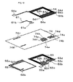
- Fig. 1 is an exploded view of a multilayer directional coupler according to an embodiment of the present invention.
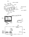
- Fig. 2 is an exterior view of the multilayer directional coupler.
- a multilayer directional coupler 1 includes a magnetic substrate 2-1 as a first magnetic substrate, a laminate 3 laminated on the magnetic substrate 2-1, a magnetic substrate 2-2 bonded as a second magnetic substrate to the laminate 3, and external electrodes 4-1 to 4-6.
- the laminate 3 includes a first transformer 5, a second transformer 6, and a nonmagnetic body 7 (see Fig. 2) that externally, completely covers the first and second transformers 5 and 6.
- the nonmagnetic body 7 is, for example, a dielectric, and is formed by laminating nonmagnetic layers "71 to 75.
- the first and second transformers 5 and 6 are pattern-formed on the nonmagnetic layers 71 to 74.
- the first transformer 5 includes a primary coil 5-1 and a secondary coil 5-2 above it.
- the primary coil 5-1 is formed by conductor patterns 51 and 52
- the secondary coil 5-2 is formed by conductor patterns 53 and 54.
- the second transformer 6 includes a primary coil 6-1 and a secondary coil 6-2 above it.
- the primary coil 6-1 is formed by conductor patterns 63 and 64
- a secondary coil 6-2 is formed by conductor patterns 61 and 62.
- the conductor patterns 51 and 64 are pattern-formed on the nonmagnetic layer 71 laminated on the magnetic substrate 2-1 by a photolithography method or the like. After the nonmagnetic layer 72 is laminated on the conductor patterns 51 and 64, the conductor patterns 52 and 63 are pattern-formed on the nonmagnetic layer 72.
- Fig. 3 is a plan view of the conductor patterns 51 and 64.
- Fig. 4 is a plan view of the nonmagnetic layer 72.
- Fig. 5 is a plan view of the conductor patterns 52 and 63.
- Fig. 6 is an exploded perspective view showing a connection structure of the conductor patterns 51 and 64, and the conductor patterns 52 and 63.
- the conductor pattern 51 includes an internal electrode 51a leading from the inside and an end portion 51b inside the pattern.
- the conductor pattern 52 includes an internal electrode 52a leading to the outside and an inside end portion 52b.
- the end portion 51b of the conductor pattern 51 is connected to the end portion 52b of the conductor pattern 52 by a through hole 72b in the nonmagnetic layer 72, which is shown also in Fig. 4.
- the conductor pattern 64 includes an internal electrode 64a leading to an outside central portion (a position corresponding to the internal electrode 52a) of the conductor pattern 51, which is next to the conductor pattern 64.
- Left-pointing end portions 64b to 64d and right-pointing end portions 64e to 64h are alternately arranged on a side opposite to a side on which the internal electrode 64a leads.
- the conductor pattern 63 includes an internal electrode 63a leading from the inside up to the center between the conductor patterns 52 and 63. Pattern end portions 63b to 63d are arranged to the left of a lead of the internal electrode 63a, and endportions 63e to 63h are arranged to the right of the lead.
- end portions 64b to 64d of the conductor pattern 64 are respectively connected to end portions 63b to 63d of the conductor pattern 63 by through holes 72b' to 72d' of the nonmagnetic layer 72, which are shown also in Fig. 4.
- end portions 64e to 64h of the conductor pattern 64 are respectively connected to end portions 63e to 63h of the conductor pattern 63 by through holes 72e' to 72h'.
- Two leads of the internal electrodes 52a and 64a are connected by a through hole 72j in the nonmagnetic layer 72.
- the conductor patterns 53 and 62 are pattern-formed on the nonmagnetic layer 73, which is laminated on the conductor patterns 52 and 63.
- the conductor patterns 54 and 61 are pattern-formed on the nonmagnetic layer 74.
- Fig. 7 is a plan view of the conductor patterns 53 and 62.
- Fig. 8 is a plan view of the nonmagnetic layer 74.
- Fig. 9 is a plan view of the conductor patterns 54 and 61.
- Fig. 10 is an exploded perspective view showing a connection structure of the conductor patterns 53 and 62, and the conductor patterns 54 and 61.
- the conductor pattern 53 includes an internal electrode 53a leading from the inside up to the center between the conductor patterns 53 and 62. End portions 53b to 53d are arranged to the right of a lead of the internal electrode 53a, and end portions 53e to 53h are arranged to the left of the lead.
- the conductor pattern 54 includes an internal electrode 54a leading to an outside central portion (a position corresponding to an internal electrode 62a) of the conductor pattern 61, which is next to the internal electrode 54.
- Right-pointing end portions 54b to 54d and left-pointing end portions 54e to 54h are alternately arranged on a side opposite to a side on which the internal electrode 54a leads.
- the end portions 53b to 53d of the conductor pattern 53 are respectively connected to the end portions 54b to 54d by through holes 74b to 74d in Lhe nonmagnetic layer 74, which is shown also in Fig. 8. Also, the end portions 53e to 53h of the conductor pattern 53 are respectively connected to the end portions 54e to 54h of the conductor pattern 54 by through holes 74e to 74h.
- the conductor pattern 62 includes an internal electrode 62a leading to the outside and an end portion 62b that is inwardly positioned.
- the conductor pattern 61 includes an internal electrode 61a leading from the inside and an inward end portion 61b.
- the end portion 62b of the conductor pattern 62 is connected to the end portion 61b of the conductor pattern 61 by a through hole 74b' in the nonmagnetic layer 74, which is shown also in Fig. 8.
- two leads of the internal electrodes 54a and 62a are connected by a through hole 74j in the nonmagnetic layer 72.
- the nonmagnetic layer 75 is laminated on the conductor patterns 54 and 61, and the magnetic substrate 2-2 is bonded to the nonmagnetic layer 75.
- External electrodes 4-1 to 4-6 are formed outside the laminate 3 having the above-described structure.
- the external electrode 4-1 to electrically connect to both the internal electrodes 52a and 64a of the conductor patterns 52 and 64, and allows the external electrode 4-2 to electrically connect to the internal electrode 51a of the conductor pattern 51.
- the external electrode 4-3 electrically connects to the internal electrode 61a of the conductor pattern 61.
- the external electrode 4-4 electrically connects to both the internal electrodes 53a and 63a of the conductor patterns 53 and 63.
- the external electrode 4-5 electrically connects to both the internal electrodes 54a and 62a of the conductor patterns 54 and 62.
- Fig. 11 is a schematic diagram showing an electrical structure of the first and second transformers 5 and 6.
- the electrical structure On the basis of the above connections between the conductor patterns and the above connections between the external electrodes 4-1 to 4-6 and the internal electrodes, the electrical structure has the circuit structure shown in Fig. 11.
- the external electrode 4-2 connected to the internal electrode 51a of the primary coil 5-1 of the first transformer 5 can be used as an input terminal for a main signal
- the external electrode 4-1 connected to the internal electrode 52a can be used as an output terminal for the main signal
- the external electrode 4-4 connected to the internal electrode 53a of the secondary coil 5-2 can be used as a ground terminal.
- the internal electrode 64a of the primary coil 6-1 of the second transformer 6 is connected to the internal electrode 52a of the primary coil
- the internal electrode 63a is connected to the internal electrode 53a of the secondary coil 5-2 of the first transformer 5.
- the internal electrode 62a of the secondary coil 6-2 is connected to the internal electrode 54a of the secondary coil 5-2 of the first transformer 5.
- the external electrode 4-3 connected to the internal electrode 61a of the secondary coil 6-2 can be used as an output terminal for a subsignal
- the external electrode 4-5 connected to both the internal electrodes 54a and 62a can be used as a terminating end by a terminating resistor or the like, which is not shown.
- This circuit structure is identical to a circuit structure of the directional coupler 100 shown in Fig. 15.
- This multilayer directional coupler has a function of distributing and outputting the main signal input from the external electrode 4-2 to the external electrode 4-1 and 4-3. Needless to say, when inputting the main signal from the external electrode 4-3, the multilayer directional coupler has a function of distributing and outputting the input main signal to the external electrodes 4-5 and 4-2.
- the multilayer directional coupler has a function of distributing and outputting the main signal.
- the distribution ratios are determined according to the degree of electromagnetic coupling occurring between the first and second transformers, such as electromagnetic coupling between the primary and secondary coils 5-1 and 5-2 of the first transformer 5, and electromagnetic coupling between the primary and secondary coils 5-1 and 6-2 of the second transformer 6.
- the degree of electromagnetic coupling is dependent on the winding length ratio N1 of the secondary coil 5-2 to the primary coil 5-1 of the first transformer 5 and the winding length ration N2 of the primary coil 6-1 to the secondary coil 6-2 of the second transformer 6.
- Fig. 12 is a graph showing the winding length ratios (N1, N2) and the degree of coupling of the multilayer directional coupler.
- N1, N2 the degree of coupling between the first and second transformers 5 and 6 had good values of approximately 2 dB to 20 dB in a range in which a winding length ratio (1N2) was not less than 1 and not greater than 10.
- the winding length ratios N1 and N2 are set so that 1 ⁇ N1 ⁇ 10 and 1 ⁇ N2 ⁇ 10.
- the primary coil 5-1 whose winding length was "4.2 mm” was pattern-formed, and the secondary coil 5-2, whose winding length was "10.5 mm” was pattern-formed, with the winding length ratio N1 set to "2.5".
- the primary coil 6-1 whose winding length was "4.2 mm” was pattern-formed, and the secondary coil 6-2, whose winding length was "10.5 mm", was pattern-formed, with the winding length ratio N2 set to "2.5".
- a ratio (N2/N1) of the winding length ratio N2 was set to "1".
- the primary and secondary coils 5-1 and 5--2 of the first transformer 5 and the primary and secondary coils 6-1 and 6-2 of the second transformer 6 can be pattern-formed so as to have preferable winding lengths. Accordingly, the winding length ratios N1 and N2 of the first and second transformers can be fine and accurately set.
- the external electrodes 4-1 and 4-2 are connected to end portions of a main line 200, with the external electrode 4-2 used as an input terminal for main signal S, and the external electrode 4-1 used as an output terminal.
- the external electrode 4-4 is set to a ground state.
- the external electrode 4-5 is grounded via a terminating resistor or the like, and the external electrode 4-3 is connected to a subline 201 and is used as an output terminal for subsignal S2.
- main signal S is input from the external electrode 4-2 to the multilayer directional coupler 1.
- main signal S1 is output from the external electrode 4-1 to the main line 200
- subsignal S2 is output from the external electrode 4-3 to thesubline201.
- main signal S input to the multilayer directional coupler 1 is distributed and output to the main line 200 and the subline 201 at an optimal distribution ratio corresponding to the winding length ratios N1 and N2 of the first and second transformers 5 and 6 and the ratio N2/N1.
- main signal S can be distributed as main signal S1 and subsignal S2 in a wide band.
- the multilayer directional coupler 1 can be used even for an apparatus that needs a signal having a bandwidth ratio equal to or greater than 90%, such as a television signal.
- the present invention is not limited to the above-described embodiment and may be variously modified and altered within the sprit of the present invention.
- each of the winding length ratios N1 and N2 may be a value that is greater than 1 and not greater than 10, and is not limited the value set in the foregoing embodiment.
- N2/N1 is set to "1"
- this ratio is not limited to this value since this ratio may be a value that is greater than 0.5 and less than 2.0.
Landscapes
- Engineering & Computer Science (AREA)
- Power Engineering (AREA)
- Microelectronics & Electronic Packaging (AREA)
- Coils Or Transformers For Communication (AREA)
Abstract
A multilayer directional coupler which is easy to mass-produce and reduce in size, in which fine setting of the degree of electromagnetic coupling is facilitated, and which has a large bandwidth ratio is provided.
A multilayer directional coupler 1 includes magnetic substrates 2-1 and 2-2, a laminate 3 including first and second transformers 5 and 6, and external electrodes 4-1 to 4-6. The electrode 4-2, which is connected to two ends of a primary coil 5-1 of the first transformer 5, is used as an input end for a main signal, and the electrode 4-1 is used as an output end. The electrode 4-3, which is connected to two ends of a secondary coil 6-2 of the second transformer 6, is used as an output end for a subsignal. A winding length ratio N1 (N2) of secondary coil 5-2 (6-1) to the primary coil 5-1 (6-2) is set to be greater than 1 and not greater than 10. Preferably, the ratio N2/N1 is set to be greater than 0.5 and less than 2.0.
Description
- The present invention relates to a multilayer directional coupler used in a mobile communication apparatus such as a cellular phone or the like.
- Multilayer directional couplers include, for example, the technologies disclosed in
Patent Documents 1 and 2. These directional couplers have a structure in which strip-line transmission lines each having a length of a quarter wavelength or not greater than a quarter wavelength are laminated and formed in a dielectric substrate. On the basis of this structure, these directional couplers can be easily mass-produced and reduced in size. Accordingly, these multilayer directional couplers are widely used in mobile communication apparatuses, etc. - However, in these directional couplers, a bandwidth at which a stable degree of electromagnetic coupling can be obtained is represented by a bandwidth ratio of 50% or less. Therefore, these multilayer directional couplers cannot be used in apparatuses that need a signal having a bandwidth ratio of 90% or greater, such as a television signal.
- Conversely, a directional coupler capable of realizing a band with ratio of 99% or greater is disclosed in Non-Patent
Document 1. - As shown in Fig. 14, this
directional coupler 100 is made by winding anelectrode 102 around a binocular-shapedmagnetic core 101, and its circuit configuration is as shown in Fig. 15. - In this configuration, by appropriately setting a winding ratio (a ratio of the numbers of turns) N1 of a
coil 112 to coil 111 of atransformer 110, and appropriately setting a winding ratio (a ratio of the numbers of turns) N2 of acoil 121 tocoil 122 of atransformer 120, for example, a main signal input from aport 110a (port 110b) of thetransformer 110 can be output to aport 110b (port 110a) and aport 120a (port 120b) of thetransformer 120 at a distribution ratio corresponding to the winding ratios. - Patent Document 1:
Japanese Unexamined Patent Application Publication No. 05-152814 - Patent Document 2:
Japanese Unexamined Patent Application Publication No. 05-160614 - Non-Patent Document 1: Michael G. Ellis, "RF Directional Couplers", Electronic System Products, Searched on May 20, 2005, Internet, http://members.tripod.com/michaelgell is/direct.html
- However, since, as shown in Fig. 14, for the
directional coupler 100, an operation of manually winding theelectrode 102 around themagnetic core 101 is needed, mass productivity is low compared with the above multilayer directional couplers. In addition, this type of directional coupler needs at least a volume of 80 mm3, and is accordingly not suitable in terms of size reduction. In addition, with thedirectional coupler 100, it is difficult to fine set the degree of electromagnetic coupling between the transformers because the degree of electromagnetic coupling between the transformers must be set on the basis of a winding ratio (a ratio of the numbers of turns) of theelectrode 102. Accordingly, a main signal input to theport 110a (theport 110b) may not be output to theport 110b (theport 110a) and theport 120a (theport 120b) of thetransformer 120 at a desired distribution ratio. - The present invention has been made in order to solve the above problems. It is an object of the present invention to provide a multilayer directional coupler which is easy to mass-produce and reduce in size, in which fine setting of the degree of electromagnetic coupling is facilitated, and which has a large bandwidth ratio is provided.
- To solve the above problems, a multilayer directional coupler described in
Claim 1 of the present invention includes a first magnetic substrate, a laminate, laminated on the first magnetic substrate, having first and second transformers formed in the laminate, and a second magnetic substrate provided on the laminate. Two ends of a primary coil of the first transformer are used as input and output terminals for a main signal, one end of a secondary coil of the first transformer is used as a ground terminal, and the other end of the secondary coil is connected to one terminal of a secondary coil of the second transformer. One end of a primary coil of the second transformer is connected to one terminal of the first transformer, the other end of the primary coil of the second transformer is connected to the ground terminal, and one terminal of the secondary coil of the second transformer is used as an output terminal for outputting a subsignal. The winding length ratio N1 of the secondary coil to primary coil of the first transformer and the winding length ratio N2 of the primary coil to secondary coil of the second transformer are each set to a value that is greater than 1 and not greater than 10. - The above-described configuration allows the multilayer directional coupler to have a multilayer structure including the first magnetic substrate, the laminate having the first and second transformers formed therein, and the second magnetic substrate. Thus, by using a known production technology such as photolithography, micro-multilayer directional couplers can be mass-produced.
- When the main signal is input to the input terminal of the primary coil of the first transformer, the main signal is distributed and output from the output terminal of the primary coil and the output terminal of the secondary coil of the second transformer. In this case, the distribution ratio is determined depending on the degree of electromagnetic coupling between the first and second transformers. The degree of electromagnetic coupling is determined on the basis of a winding length ratio N1 of the secondary coil to first coil of the first transformer and a winding length ratio N2 of the primary coil to secondary coil of the second transformer. Accordingly, in the present invention, the winding length ratios N1 and N2 are each set to a value that is greater than 1 and not greater than 10.
- In addition, since the first and second transformers can be formed by a known technology such as photolithography, the lengths of the coils of the first and second transformers can be pattern-formed so as to have preferable values. Accordingly, differently from the
directional coupler 100 of the related art, the winding length ratios N1 and N2 of the first and second transformers can be fine set, thus enabling fine setting of the degree of electromagnetic coupling. - Further, the two ends of the primary coil of the first transformer are used as the input and output terminals for the main signal, one end of the secondary coil of the first transformer is used as the ground terminal, and the other end of the secondary coil is connected to one terminal of the secondary coil of the second transformer. One end of a primary coil of the second transformer is connected to one terminal of the first transformer, the other end of the primary coil of the second transformer is connected to the ground terminal, and one terminal of the secondary coil of the second transformer is used as the output terminal for outputting the subsignal. Thus, the multilayer directional coupler can be used even for an apparatus that needs a signal having a bandwidth ratio equal to or greater than 90%, such as a television signal.
- In Claim 2 of the present invention, in the multilayer directional coupler described in
Claim 1, the ratio of the winding length ratio N2 to the winding length ratio N1 is set to a value that is greater than 0.5 and less than 2.0. - In
Claim 3 of the present invention, in the multilayer directional coupler described inClaim 1 or 2, the laminate is formed by covering the first and second transformers with a nonmagnetic body. - As described above in detail, according to
Claims 1 to 3 of the present invention, the present invention has a good advantage in that it can provide a multilayer directional coupler which is easy to mass-produce and reduce in size, in which fine setting of the degree of electromagnetic coupling between the first and second transformers is facilitated, and which has a large bandwidth ratio. - In particular, according to Claim 2 of the present invention, since the ratio of the winding length ratio N2 to the winding length ratio N1 is set to a value that is greater than 0.5 and less than 2.0, an advantage is obtained in that a multilayer directional coupler in which the degree of electromagnetic coupling and directionality between the first and second transformers can be fine adjusted.
-
- Fig. 1 is an exploded perspective view of a multilayer directional coupler according to an embodiment of the present invention.
- Fig. 2 is an exterior view of the multilayer directional coupler.
- Fig. 3 is a plan view of a conductor pattern of a bottom layer.
- Fig. 4 is a plan view of a nonmagnetic layer.
- Fig. 5 is a plan view of a conductor pattern of the second layer from the bottom.
- Fig. 6 is an exploded perspective view showing a connection structure of the conductor pattern of the bottom layer and the conductor pattern of the second layer.
- Fig. 7 is a plan view of a conductor pattern of the third layer from the bottom.
- Fig. 8 is a plan view of a nonmagnetic layer.
- Fig. 9 is a plan view of a conductor pattern of a top layer.
- Fig. 10 is an exploded perspective view showing a connection structure of the conductor pattern of the third layer and the conductor pattern of the top layer.
- Fig. 11 is a schematic diagram showing an electrical structure of first and second transformers.
- Fig. 12 is a graph showing a winging length ratio of coils and the degree of coupling between the first and second transformers.
- Fig. 13 is a perspective view showing a mounting state of a multilayer directional coupler.
- Fig. 14 is a perspective view showing an example of a directional coupler of the related art.
- Fig. 15 is an equivalent circuit diagram of the directional coupler in Fig. 14.
-
- 1
- multilayer directional coupler
- 2-1, 2-2
- magnetic substrates
- 3
- laminate
- 4-1 to 4-6
- external electrodes
- 5
- first transformer
- 5-1,
- 6-1 primary coils
- 6
- second transformer
- 7
- nonmagnetic material
- 51 to 54, 61 to 64
- conductor patterns
- 51a to 54a, 61a to 64a
- internal electrodes
- 51b to 51h, 52b to 52h, 53b to 53h, 54b to 54h, 61b to 61h, 62b to 62h, 63b to 63h, 64b to 64h
- end portions
- 72b to 72h, 72j, 72b' to 72h', 74b to 74h, 74j, 74b' to 74h'
- through holes
- 71 to 75
- nonmagnetic layers
- 200
- main line
- 201
- subline
- S, S1
- main signals
- S2
- subsignal
- A best mode of the invention is described below with reference to the drawings.
- Fig. 1 is an exploded view of a multilayer directional coupler according to an embodiment of the present invention. Fig. 2 is an exterior view of the multilayer directional coupler.
- As shown in Fig.2, a multilayer
directional coupler 1 according to the embodiment includes a magnetic substrate 2-1 as a first magnetic substrate, alaminate 3 laminated on the magnetic substrate 2-1, a magnetic substrate 2-2 bonded as a second magnetic substrate to thelaminate 3, and external electrodes 4-1 to 4-6. - As shown in Fig. 1, the
laminate 3 includes afirst transformer 5, asecond transformer 6, and a nonmagnetic body 7 (see Fig. 2) that externally, completely covers the first andsecond transformers - The
nonmagnetic body 7 is, for example, a dielectric, and is formed by laminating nonmagnetic layers "71 to 75. The first andsecond transformers nonmagnetic layers 71 to 74. - Specifically, the
first transformer 5 includes a primary coil 5-1 and a secondary coil 5-2 above it. The primary coil 5-1 is formed byconductor patterns conductor patterns - In addition, the
second transformer 6 includes a primary coil 6-1 and a secondary coil 6-2 above it. The primary coil 6-1 is formed byconductor patterns conductor patterns - Here, structures of the first and
second transformers - The
conductor patterns nonmagnetic layer 71 laminated on the magnetic substrate 2-1 by a photolithography method or the like. After thenonmagnetic layer 72 is laminated on theconductor patterns conductor patterns nonmagnetic layer 72. - Fig. 3 is a plan view of the
conductor patterns nonmagnetic layer 72. Fig. 5 is a plan view of theconductor patterns conductor patterns conductor patterns - As shown in Fig. 3, the
conductor pattern 51 includes aninternal electrode 51a leading from the inside and anend portion 51b inside the pattern. As shown in Fig. 5, theconductor pattern 52 includes aninternal electrode 52a leading to the outside and aninside end portion 52b. - As shown in Fig. 6, the
end portion 51b of theconductor pattern 51 is connected to theend portion 52b of theconductor pattern 52 by a throughhole 72b in thenonmagnetic layer 72, which is shown also in Fig. 4. This forms the primary coil 5-1, which is spiral, and which uses theinternal electrodes - In addition, as shown in Fig. 3, the
conductor pattern 64 includes aninternal electrode 64a leading to an outside central portion (a position corresponding to theinternal electrode 52a) of theconductor pattern 51, which is next to theconductor pattern 64. Left-pointingend portions 64b to 64d and right-pointingend portions 64e to 64h are alternately arranged on a side opposite to a side on which theinternal electrode 64a leads. As shown in Fig. 5, theconductor pattern 63 includes aninternal electrode 63a leading from the inside up to the center between theconductor patterns Pattern end portions 63b to 63d are arranged to the left of a lead of theinternal electrode 63a, andendportions 63e to 63h are arranged to the right of the lead. As shown in Fig. 6, endportions 64b to 64d of theconductor pattern 64 are respectively connected to endportions 63b to 63d of theconductor pattern 63 by throughholes 72b' to 72d' of thenonmagnetic layer 72, which are shown also in Fig. 4. Also,end portions 64e to 64h of theconductor pattern 64 are respectively connected to endportions 63e to 63h of theconductor pattern 63 by throughholes 72e' to 72h'. This forms the primary coil 6-1, which is spiral, and which uses theinternal electrodes - Two leads of the
internal electrodes hole 72j in thenonmagnetic layer 72. - In addition, as shown in Fig. 1, the
conductor patterns nonmagnetic layer 73, which is laminated on theconductor patterns nonmagnetic layer 74 is laminated on theconductor patterns conductor patterns nonmagnetic layer 74. - Fig. 7 is a plan view of the
conductor patterns nonmagnetic layer 74. Fig. 9 is a plan view of theconductor patterns conductor patterns conductor patterns - As shown in Fig. 7, the
conductor pattern 53 includes aninternal electrode 53a leading from the inside up to the center between theconductor patterns End portions 53b to 53d are arranged to the right of a lead of theinternal electrode 53a, andend portions 53e to 53h are arranged to the left of the lead. In addition, as shown in Fig. 9, theconductor pattern 54 includes aninternal electrode 54a leading to an outside central portion (a position corresponding to aninternal electrode 62a) of theconductor pattern 61, which is next to theinternal electrode 54. Right-pointingend portions 54b to 54d and left-pointingend portions 54e to 54h are alternately arranged on a side opposite to a side on which theinternal electrode 54a leads. - As shown in Fig. 10, the
end portions 53b to 53d of theconductor pattern 53 are respectively connected to theend portions 54b to 54d by throughholes 74b to 74d in Lhenonmagnetic layer 74, which is shown also in Fig. 8. Also, theend portions 53e to 53h of theconductor pattern 53 are respectively connected to theend portions 54e to 54h of theconductor pattern 54 by throughholes 74e to 74h. This forms the secondary coil 5-2, which is spiral, and which uses theinternal electrodes - In addition, as shown in Fig. 7, the
conductor pattern 62 includes aninternal electrode 62a leading to the outside and anend portion 62b that is inwardly positioned. Also, as shown in Fig. 9, theconductor pattern 61 includes aninternal electrode 61a leading from the inside and aninward end portion 61b. As shown in Fig. 10, theend portion 62b of theconductor pattern 62 is connected to theend portion 61b of theconductor pattern 61 by a throughhole 74b' in thenonmagnetic layer 74, which is shown also in Fig. 8. This forms the secondary coil 6-2, which is spiral, and which uses theinternal electrodes - In addition, two leads of the
internal electrodes hole 74j in thenonmagnetic layer 72. - As shown in Fig. 1, the
nonmagnetic layer 75 is laminated on theconductor patterns nonmagnetic layer 75. - External electrodes 4-1 to 4-6 are formed outside the
laminate 3 having the above-described structure. - This allows the external electrode 4-1 to electrically connect to both the
internal electrodes conductor patterns internal electrode 51a of theconductor pattern 51. Also, the external electrode 4-3 electrically connects to theinternal electrode 61a of theconductor pattern 61. The external electrode 4-4 electrically connects to both theinternal electrodes conductor patterns internal electrodes conductor patterns - Fig. 11 is a schematic diagram showing an electrical structure of the first and
second transformers - On the basis of the above connections between the conductor patterns and the above connections between the external electrodes 4-1 to 4-6 and the internal electrodes, the electrical structure has the circuit structure shown in Fig. 11.
- In other words, the external electrode 4-2 connected to the
internal electrode 51a of the primary coil 5-1 of thefirst transformer 5 can be used as an input terminal for a main signal, and the external electrode 4-1 connected to theinternal electrode 52a can be used as an output terminal for the main signal. The external electrode 4-4 connected to theinternal electrode 53a of the secondary coil 5-2 can be used as a ground terminal. Theinternal electrode 64a of the primary coil 6-1 of thesecond transformer 6 is connected to theinternal electrode 52a of the primary coil, and theinternal electrode 63a is connected to theinternal electrode 53a of the secondary coil 5-2 of thefirst transformer 5. Theinternal electrode 62a of the secondary coil 6-2 is connected to theinternal electrode 54a of the secondary coil 5-2 of thefirst transformer 5. Accordingly, the external electrode 4-3 connected to theinternal electrode 61a of the secondary coil 6-2 can be used as an output terminal for a subsignal, and the external electrode 4-5 connected to both theinternal electrodes - This circuit structure is identical to a circuit structure of the
directional coupler 100 shown in Fig. 15. This multilayer directional coupler has a function of distributing and outputting the main signal input from the external electrode 4-2 to the external electrode 4-1 and 4-3. Needless to say, when inputting the main signal from the external electrode 4-3, the multilayer directional coupler has a function of distributing and outputting the input main signal to the external electrodes 4-5 and 4-2. - As described above, the multilayer directional coupler has a function of distributing and outputting the main signal. The distribution ratios are determined according to the degree of electromagnetic coupling occurring between the first and second transformers, such as electromagnetic coupling between the primary and secondary coils 5-1 and 5-2 of the
first transformer 5, and electromagnetic coupling between the primary and secondary coils 5-1 and 6-2 of thesecond transformer 6. The degree of electromagnetic coupling is dependent on the winding length ratio N1 of the secondary coil 5-2 to the primary coil 5-1 of thefirst transformer 5 and the winding length ration N2 of the primary coil 6-1 to the secondary coil 6-2 of thesecond transformer 6. - Fig. 12 is a graph showing the winding length ratios (N1, N2) and the degree of coupling of the multilayer directional coupler. As a result of performing simulation in order to know a range of the winding length ratios (N1, N2) at which the first and second transformers have a good degree of coupling therebetween, the present inventors obtained the results shown in Fig. 12. Specifically, it was found that, as indicated by curve S in Fig. 12, the degree of coupling between the first and
second transformers - Specifically, in this embodiment, the primary coil 5-1, whose winding length was "4.2 mm" was pattern-formed, and the secondary coil 5-2, whose winding length was "10.5 mm" was pattern-formed, with the winding length ratio N1 set to "2.5". Also, the primary coil 6-1, whose winding length was "4.2 mm", was pattern-formed, and the secondary coil 6-2, whose winding length was "10.5 mm", was pattern-formed, with the winding length ratio N2 set to "2.5". In addition, by setting a ratio (N2/N1) of the winding length ratio N2 to the winding length ratio N1 so that 0.5 < N2/N1 < 2. 0, an impedance of each port can be improved. Accordingly, in this embodiment, the ratio N2/N1 was set to "1".
- In this embodiment, since the first and
second transformers first transformer 5 and the primary and secondary coils 6-1 and 6-2 of thesecond transformer 6 can be pattern-formed so as to have preferable winding lengths. Accordingly, the winding length ratios N1 and N2 of the first and second transformers can be fine and accurately set. - Next, an operation and advantages exhibited by the multilayer directional coupler according to the embodiment are described.
- As shown in Fig. 13, the external electrodes 4-1 and 4-2 are connected to end portions of a
main line 200, with the external electrode 4-2 used as an input terminal for main signal S, and the external electrode 4-1 used as an output terminal. The external electrode 4-4 is set to a ground state. The external electrode 4-5 is grounded via a terminating resistor or the like, and the external electrode 4-3 is connected to asubline 201 and is used as an output terminal for subsignal S2. - Accordingly, by transmitting main signal S through the
main line 200, main signal S is input from the external electrode 4-2 to the multilayerdirectional coupler 1. Then, main signal S1 is output from the external electrode 4-1 to themain line 200, and subsignal S2 is output from the external electrode 4-3 to thesubline201. In other words, main signal S input to the multilayerdirectional coupler 1 is distributed and output to themain line 200 and thesubline 201 at an optimal distribution ratio corresponding to the winding length ratios N1 and N2 of the first andsecond transformers - With the first and
second transformers directional coupler 100 having the circuit structure in Fig. 15, main signal S can be distributed as main signal S1 and subsignal S2 in a wide band. Thus, the multilayerdirectional coupler 1 can be used even for an apparatus that needs a signal having a bandwidth ratio equal to or greater than 90%, such as a television signal. - The present invention is not limited to the above-described embodiment and may be variously modified and altered within the sprit of the present invention.
- For example, although, in the foregoing embodiment, the winding length ratio N1 (winding length ratio N2) of the secondary coil5-2 (the primary coil 6-1) to the primary coil 5-1 (the secondary coil 6-2) of the first transformer 5 (the second transformer 6) is set to "2.5" ("2.5"), each of the winding length ratios N1 and N2 may be a value that is greater than 1 and not greater than 10, and is not limited the value set in the foregoing embodiment. In addition, although N2/N1 is set to "1", this ratio is not limited to this value since this ratio may be a value that is greater than 0.5 and less than 2.0.
Claims (3)
- A multilayer directional coupler comprising a first magnetic substrate, a laminate, laminated on the first magnetic substrate, having first and second transformers formed in the laminate, and a second magnetic substrate provided on the laminate,
wherein:two ends of a primary coil of the first transformer are used as input and output terminals for a main signal, one end of a secondary coil of the first transformer is used as a ground terminal, and the other end of the secondary coil is connected to one terminal of a secondary coil of the second transformer;one end of a primary coil of the second transformer is connected to one terminal of the first transformer, the other end of the primary coil of the second transformer is connected to the ground terminal, and one terminal of the secondary coil of the second transformer is used as an out put terminal for out putting a subsignal; anda winding length ratio N1 of the secondary coil to primary coil of the first transformer and a winding length ratio N2 of the primary coil to secondary coil of the second transformer are each set to a value that is greater than 1 and not greater than 10. - The multilayer directional coupler according to Claim 1, wherein the ratio of the winding length ratio N2 to the winding length ratio N1 is set to a value that is greater than 0.5 and less than 2.0.
- The multilayer directional coupler according to Claim 1 or 2, wherein the laminate is formed by covering the first and second transformers with a nonmagnetic body.
Applications Claiming Priority (2)
| Application Number | Priority Date | Filing Date | Title |
|---|---|---|---|
| JP2005148725 | 2005-05-20 | ||
| PCT/JP2006/307094 WO2006123482A1 (en) | 2005-05-20 | 2006-04-04 | Multilayer directional coupler |
Publications (1)
| Publication Number | Publication Date |
|---|---|
| EP1884963A1 true EP1884963A1 (en) | 2008-02-06 |
Family
ID=37431064
Family Applications (1)
| Application Number | Title | Priority Date | Filing Date |
|---|---|---|---|
| EP06731042A Withdrawn EP1884963A1 (en) | 2005-05-20 | 2006-04-04 | Multilayer directional coupler |
Country Status (4)
| Country | Link |
|---|---|
| US (1) | US7504907B2 (en) |
| EP (1) | EP1884963A1 (en) |
| JP (1) | JPWO2006123482A1 (en) |
| WO (1) | WO2006123482A1 (en) |
Families Citing this family (4)
| Publication number | Priority date | Publication date | Assignee | Title |
|---|---|---|---|---|
| JP2008199196A (en) * | 2007-02-09 | 2008-08-28 | Murata Mfg Co Ltd | Mounting structure of directional coupler, and directional coupler |
| CN103283086B (en) * | 2011-01-12 | 2015-07-29 | 株式会社村田制作所 | Directional coupler |
| US9905902B2 (en) | 2014-07-24 | 2018-02-27 | Skyworks Solutions, Inc. | Zero insertion loss directional coupler for wireless transceivers with integrated power amplifiers |
| WO2017022284A1 (en) * | 2015-08-03 | 2017-02-09 | 株式会社村田製作所 | Isolated-type dc-dc converter |
Family Cites Families (16)
| Publication number | Priority date | Publication date | Assignee | Title |
|---|---|---|---|---|
| JP2810812B2 (en) * | 1991-02-15 | 1998-10-15 | 松下電工株式会社 | Branch circuit |
| JP3274695B2 (en) * | 1991-11-15 | 2002-04-15 | 松下電工株式会社 | Flat type transformer |
| JPH05152814A (en) * | 1991-11-27 | 1993-06-18 | Murata Mfg Co Ltd | Chip type directional coupler |
| JP2817487B2 (en) * | 1991-12-09 | 1998-10-30 | 株式会社村田製作所 | Chip type directional coupler |
| JPH05258977A (en) | 1992-03-13 | 1993-10-08 | Matsushita Electric Works Ltd | Flat transformer |
| US5525941A (en) * | 1993-04-01 | 1996-06-11 | General Electric Company | Magnetic and electromagnetic circuit components having embedded magnetic material in a high density interconnect structure |
| JPH07142256A (en) * | 1993-11-19 | 1995-06-02 | Yokogawa Electric Corp | Laminated printed coil and method of manufacturing the same |
| JPH08306532A (en) * | 1995-04-28 | 1996-11-22 | Matsushita Electric Works Ltd | Branch transformer |
| JPH09139315A (en) * | 1995-11-13 | 1997-05-27 | Matsushita Electric Ind Co Ltd | Balun element |
| JPH1154336A (en) * | 1997-08-04 | 1999-02-26 | Tdk Corp | Chip-type distributing transformer |
| JP3520411B2 (en) * | 1999-11-10 | 2004-04-19 | 株式会社村田製作所 | High frequency components using coupled lines |
| JP4360044B2 (en) * | 2001-05-02 | 2009-11-11 | 株式会社村田製作所 | Multilayer directional coupler |
| JP2003168904A (en) * | 2001-11-30 | 2003-06-13 | Kyocera Corp | Balun transformer |
| JP2004015281A (en) | 2002-06-05 | 2004-01-15 | Matsushita Electric Ind Co Ltd | Directional coupler |
| JP2005085997A (en) * | 2003-09-09 | 2005-03-31 | Murata Mfg Co Ltd | Coil component |
| JP4154730B2 (en) | 2003-11-14 | 2008-09-24 | 株式会社村田製作所 | Directional coupler |
-
2006
- 2006-04-04 EP EP06731042A patent/EP1884963A1/en not_active Withdrawn
- 2006-04-04 WO PCT/JP2006/307094 patent/WO2006123482A1/en not_active Ceased
- 2006-04-04 JP JP2007516222A patent/JPWO2006123482A1/en active Pending
-
2007
- 2007-11-16 US US11/941,216 patent/US7504907B2/en not_active Expired - Lifetime
Non-Patent Citations (1)
| Title |
|---|
| See references of WO2006123482A1 * |
Also Published As
| Publication number | Publication date |
|---|---|
| JPWO2006123482A1 (en) | 2008-12-25 |
| WO2006123482A1 (en) | 2006-11-23 |
| US7504907B2 (en) | 2009-03-17 |
| US20080062723A1 (en) | 2008-03-13 |
Similar Documents
| Publication | Publication Date | Title |
|---|---|---|
| US6388551B2 (en) | Method of making a laminated balun transform | |
| US9077061B2 (en) | Directional coupler | |
| JP4500840B2 (en) | Multilayer balun and hybrid integrated circuit module and multilayer substrate | |
| US8773232B2 (en) | High-frequency transformer, high-frequency component, and communication terminal device | |
| JP2003204203A (en) | Filter with directional coupler and communication device | |
| US8212630B2 (en) | Thin film balun | |
| US7579923B2 (en) | Laminated balun transformer | |
| JP3531603B2 (en) | High frequency filter, filter device using the same, and electronic device using the same | |
| US9281797B2 (en) | High-frequency device and directional coupler | |
| US9300023B2 (en) | Thin film balun | |
| US6850127B2 (en) | Laminated electronic component | |
| US7439842B2 (en) | Laminated balun transformer | |
| CN100502144C (en) | Layered Balun | |
| KR100476561B1 (en) | Laminated balun transformer | |
| US7504907B2 (en) | Multilayer directional coupler | |
| JP2016134779A (en) | Directional coupler and module using the same | |
| JP2009004606A (en) | Balun transformer and characteristic adjustment method thereof | |
| JP2001176726A (en) | Balun transformer | |
| JP2001006941A (en) | High frequency transformer and impedance converter | |
| JP5326880B2 (en) | Thin film balun | |
| JP2016100797A (en) | Filter integrated coupler and communication module | |
| JPH06152305A (en) | Directional coupler and branching circuit | |
| JP2008199196A (en) | Mounting structure of directional coupler, and directional coupler | |
| JP2001024407A (en) | Balance/unbalance converter | |
| JP2004364178A (en) | Passive components |
Legal Events
| Date | Code | Title | Description |
|---|---|---|---|
| PUAI | Public reference made under article 153(3) epc to a published international application that has entered the european phase |
Free format text: ORIGINAL CODE: 0009012 |
|
| 17P | Request for examination filed |
Effective date: 20071218 |
|
| AK | Designated contracting states |
Kind code of ref document: A1 Designated state(s): AT BE BG CH CY CZ DE DK EE ES FI FR GB GR HU IE IS IT LI LT LU LV MC NL PL PT RO SE SI SK TR |
|
| DAX | Request for extension of the european patent (deleted) | ||
| STAA | Information on the status of an ep patent application or granted ep patent |
Free format text: STATUS: THE APPLICATION HAS BEEN WITHDRAWN |
|
| 18W | Application withdrawn |
Effective date: 20100806 |