EP1884910A1 - Active matrix substrate, display device, and pixel defect correcting method - Google Patents
Active matrix substrate, display device, and pixel defect correcting method Download PDFInfo
- Publication number
- EP1884910A1 EP1884910A1 EP06746661A EP06746661A EP1884910A1 EP 1884910 A1 EP1884910 A1 EP 1884910A1 EP 06746661 A EP06746661 A EP 06746661A EP 06746661 A EP06746661 A EP 06746661A EP 1884910 A1 EP1884910 A1 EP 1884910A1
- Authority
- EP
- European Patent Office
- Prior art keywords
- section
- pixel
- active matrix
- matrix substrate
- electrode
- Prior art date
- Legal status (The legal status is an assumption and is not a legal conclusion. Google has not performed a legal analysis and makes no representation as to the accuracy of the status listed.)
- Granted
Links
Images








Classifications
-
- G—PHYSICS
- G02—OPTICS
- G02F—OPTICAL DEVICES OR ARRANGEMENTS FOR THE CONTROL OF LIGHT BY MODIFICATION OF THE OPTICAL PROPERTIES OF THE MEDIA OF THE ELEMENTS INVOLVED THEREIN; NON-LINEAR OPTICS; FREQUENCY-CHANGING OF LIGHT; OPTICAL LOGIC ELEMENTS; OPTICAL ANALOGUE/DIGITAL CONVERTERS
- G02F1/00—Devices or arrangements for the control of the intensity, colour, phase, polarisation or direction of light arriving from an independent light source, e.g. switching, gating or modulating; Non-linear optics
- G02F1/01—Devices or arrangements for the control of the intensity, colour, phase, polarisation or direction of light arriving from an independent light source, e.g. switching, gating or modulating; Non-linear optics for the control of the intensity, phase, polarisation or colour
- G02F1/13—Devices or arrangements for the control of the intensity, colour, phase, polarisation or direction of light arriving from an independent light source, e.g. switching, gating or modulating; Non-linear optics for the control of the intensity, phase, polarisation or colour based on liquid crystals, e.g. single liquid crystal display cells
- G02F1/133—Constructional arrangements; Operation of liquid crystal cells; Circuit arrangements
- G02F1/136—Liquid crystal cells structurally associated with a semi-conducting layer or substrate, e.g. cells forming part of an integrated circuit
- G02F1/1362—Active matrix addressed cells
- G02F1/136259—Repairing; Defects
-
- G—PHYSICS
- G02—OPTICS
- G02F—OPTICAL DEVICES OR ARRANGEMENTS FOR THE CONTROL OF LIGHT BY MODIFICATION OF THE OPTICAL PROPERTIES OF THE MEDIA OF THE ELEMENTS INVOLVED THEREIN; NON-LINEAR OPTICS; FREQUENCY-CHANGING OF LIGHT; OPTICAL LOGIC ELEMENTS; OPTICAL ANALOGUE/DIGITAL CONVERTERS
- G02F1/00—Devices or arrangements for the control of the intensity, colour, phase, polarisation or direction of light arriving from an independent light source, e.g. switching, gating or modulating; Non-linear optics
- G02F1/01—Devices or arrangements for the control of the intensity, colour, phase, polarisation or direction of light arriving from an independent light source, e.g. switching, gating or modulating; Non-linear optics for the control of the intensity, phase, polarisation or colour
- G02F1/13—Devices or arrangements for the control of the intensity, colour, phase, polarisation or direction of light arriving from an independent light source, e.g. switching, gating or modulating; Non-linear optics for the control of the intensity, phase, polarisation or colour based on liquid crystals, e.g. single liquid crystal display cells
- G02F1/133—Constructional arrangements; Operation of liquid crystal cells; Circuit arrangements
- G02F1/136—Liquid crystal cells structurally associated with a semi-conducting layer or substrate, e.g. cells forming part of an integrated circuit
- G02F1/1362—Active matrix addressed cells
- G02F1/1368—Active matrix addressed cells in which the switching element is a three-electrode device
-
- G—PHYSICS
- G02—OPTICS
- G02F—OPTICAL DEVICES OR ARRANGEMENTS FOR THE CONTROL OF LIGHT BY MODIFICATION OF THE OPTICAL PROPERTIES OF THE MEDIA OF THE ELEMENTS INVOLVED THEREIN; NON-LINEAR OPTICS; FREQUENCY-CHANGING OF LIGHT; OPTICAL LOGIC ELEMENTS; OPTICAL ANALOGUE/DIGITAL CONVERTERS
- G02F1/00—Devices or arrangements for the control of the intensity, colour, phase, polarisation or direction of light arriving from an independent light source, e.g. switching, gating or modulating; Non-linear optics
- G02F1/01—Devices or arrangements for the control of the intensity, colour, phase, polarisation or direction of light arriving from an independent light source, e.g. switching, gating or modulating; Non-linear optics for the control of the intensity, phase, polarisation or colour
- G02F1/13—Devices or arrangements for the control of the intensity, colour, phase, polarisation or direction of light arriving from an independent light source, e.g. switching, gating or modulating; Non-linear optics for the control of the intensity, phase, polarisation or colour based on liquid crystals, e.g. single liquid crystal display cells
- G02F1/133—Constructional arrangements; Operation of liquid crystal cells; Circuit arrangements
- G02F1/136—Liquid crystal cells structurally associated with a semi-conducting layer or substrate, e.g. cells forming part of an integrated circuit
-
- H—ELECTRICITY
- H10—SEMICONDUCTOR DEVICES; ELECTRIC SOLID-STATE DEVICES NOT OTHERWISE PROVIDED FOR
- H10D—INORGANIC ELECTRIC SEMICONDUCTOR DEVICES
- H10D30/00—Field-effect transistors [FET]
- H10D30/60—Insulated-gate field-effect transistors [IGFET]
- H10D30/67—Thin-film transistors [TFT]
- H10D30/6729—Thin-film transistors [TFT] characterised by the electrodes
-
- H—ELECTRICITY
- H10—SEMICONDUCTOR DEVICES; ELECTRIC SOLID-STATE DEVICES NOT OTHERWISE PROVIDED FOR
- H10D—INORGANIC ELECTRIC SEMICONDUCTOR DEVICES
- H10D86/00—Integrated devices formed in or on insulating or conducting substrates, e.g. formed in silicon-on-insulator [SOI] substrates or on stainless steel or glass substrates
-
- H—ELECTRICITY
- H10—SEMICONDUCTOR DEVICES; ELECTRIC SOLID-STATE DEVICES NOT OTHERWISE PROVIDED FOR
- H10D—INORGANIC ELECTRIC SEMICONDUCTOR DEVICES
- H10D86/00—Integrated devices formed in or on insulating or conducting substrates, e.g. formed in silicon-on-insulator [SOI] substrates or on stainless steel or glass substrates
- H10D86/40—Integrated devices formed in or on insulating or conducting substrates, e.g. formed in silicon-on-insulator [SOI] substrates or on stainless steel or glass substrates characterised by multiple TFTs
- H10D86/441—Interconnections, e.g. scanning lines
-
- H—ELECTRICITY
- H10—SEMICONDUCTOR DEVICES; ELECTRIC SOLID-STATE DEVICES NOT OTHERWISE PROVIDED FOR
- H10D—INORGANIC ELECTRIC SEMICONDUCTOR DEVICES
- H10D86/00—Integrated devices formed in or on insulating or conducting substrates, e.g. formed in silicon-on-insulator [SOI] substrates or on stainless steel or glass substrates
- H10D86/40—Integrated devices formed in or on insulating or conducting substrates, e.g. formed in silicon-on-insulator [SOI] substrates or on stainless steel or glass substrates characterised by multiple TFTs
- H10D86/60—Integrated devices formed in or on insulating or conducting substrates, e.g. formed in silicon-on-insulator [SOI] substrates or on stainless steel or glass substrates characterised by multiple TFTs wherein the TFTs are in active matrices
Definitions
- the present invention relates to an active matrix substrate for various display apparatuses, such as a liquid crystal display apparatus, EL (Electro Luminescence) display apparatus etc. More specifically, the present invention relates to an active matrix substrate suitable for a liquid crystal display apparatus with a large liquid crystal display screen, such as a large-size liquid crystal television.
- An active matrix substrate is widely used for various active matrix display apparatuses such as a liquid crystal display apparatus, an EL (Electro Luminescence) display apparatus etc.
- a switching element such as a TFT (Thin Film Transistor) is provided in each intersection of a plurality of scanning signal lines and a plurality of data signal lines which are intersect with each other on a base substrate.
- TFT Thin Film Transistor
- the retention capacitor element is also used as a supply path of various modulation signals for driving liquid crystal.
- Figure 18 is a schematic plan view showing a single pixel of an active matrix substrate of a conventional active matrix liquid crystal display apparatus.
- a plurality of pixel electrodes 51 are arranged in matrix, surrounded by scanning signal lines 52 for supplying scanning signals, and data signal lines 53 for supplying data signals, which intersect with each other.
- a TFT 54 is provided in each intersection of the scanning signal lines 52 and the data signal lines 53.
- the TFT 54 serves as a switching element connected to the pixel electrode 51.
- the gate electrode 55 of the TFT 54 is connected to the scanning signal lines 52 through which scanning signals are supplied. In this manner the driving of TFT 54 is controlled.
- the source electrode 66a of the TFT 54 is connected to the data signal lines 53 through which data signals are supplied.
- drain wire 56 is connected to the drain electrode 66b of the TFT 54, the drain wire 56 is also connected to one of the electrodes (retention capacitor upper electrode) 57 of the retention capacitor element, and the retention capacitor electrode 57 is connected to a pixel electrode 51 via a contact hole 58.
- a retention capacitor (common) wire 59 serves as the other one (retention capacitor lower electrode) of the two electrodes of the retention capacitor element.
- the liquid crystal display apparatus used for a large-sized liquid crystal TV often adopts a Vertical Alignment (VA) mode having a multi-domain, or so-called a Multi-domain Vertical Alignment (MVA) mode, so as to ensure a wide viewing angle (see Document 2, for example).
- VA Vertical Alignment
- MVA Multi-domain Vertical Alignment
- the pixel electrodes of the active matrix substrate and the counter electrodes of the counter substrate are provided with an exsection pattern or an alignment control projection for adjusting alignment of liquid crystal molecules from which a fringe field is formed. Provision of fringe field has an effect of scattering the liquid crystal molecules so that they are aligned into plural directions. This is how the wide viewing angle is ensured.
- the conventional active matrix substrate shown in Figure 18 ensures a wide viewing angle by having an exsection pattern or an alignment control projection for adjusting alignment of liquid crystal molecules in each of the pixel electrodes of the active matrix substrate and the counter electrodes of the counter substrate.
- this technique carries out laser irradiation with respect to the correction connection wiring so as to allow the pixel electrode of the defective pixel to be electrically conducted to the pixel electrode of the adjacent pixel. In this way, the voltage equal in potential to that of the adjacent pixel is supplied to the defective pixel, and the defective pixel is driven by a pseudo operation.
- this method needs to be improved to solve the following problem.
- the pixels are insulated with each other, and therefore the correction connection wirings are required to be formed across the pixels. Therefore, as the area of the correction connection wiring increases, the aperture ratio decreases.
- the sporadic short-circuit (leak) between the source electrode and the drain electrode of the TFT it is preferable to compensate the error within the pixel in which the defect occurs. This is because, if the defective pixel is driven by the TFT of the adjacent pixel via the correction connection wiring after the leakage portion is cut off, an extra driving load is exerted on the TFT of the adjacent pixel.
- the defect of the pixel can be corrected only by connecting adjacent pixels.
- the present invention is made in view of the foregoing problems, and an object is to provide an active matrix substrate which does not cause a decrease in aperture ratio even in the case of correcting defects within the pixel. With this feature, the present invention provides an active matrix substrate which significantly reduces disconnection of electrodes from the signal line.
- An active matrix substrate includes an active element having at least one source electrode, two or more drain electrodes, and two or more channels, at least one of said drain electrodes is electrically connected to a pixel electrode via a wire section, said wire section (drain outgoing wire) includes a first conductive pattern section having a common section (drain outgoing wire common section) continuous to a pixel electrode and branch sections (drain outgoing wire branch section) each of which extends from said common section and is broken into each of said drain electrodes, said active matrix substrate further including a second conductive pattern section which has an overlapping portion overlapped with said branch sections of said first conductive pattern section via an insulating layer, said second conductive pattern section being electrically connectable to a plurality of said branch sections by being conducted to said overlapping portion through said insulating layer.
- the active elements are not required to be aligned in parallel, as in Figure 1 of Document 5.
- the layout of electrode becomes simpler, and the aperture ratio does not decrease because of the source electrode.
- pixel defect correction within a pixel becomes possible with a low probability of disconnection of the electrodes.
- Such a wire layout of active element is suitable for a structure in which two or more of the branch sections (drain outgoing wire branch section) are connected to the active element.
- an active element with two or more of drain electrodes is identical to an active element with the same number of channels.
- pixel defect caused by some kind of defect (such as a leak) in a channel can be modified by using another proper channel within the same active element.
- the branch section (drain outgoing wire branch section) connected to the channel is cut, and then the separated branch section (drain outgoing wire branch section) is connected (drain/drain connection) into a branch section (drain outgoing wire branch section) connected to a proper channel via the correction connection electrode.
- all of the branch sections (drain outgoing wire branch section) may be supplied with substantially the same drain potentials.
- this arrangement allows provision of a plurality of branch sections (drain outgoing wire branch section), thereby providing redundant paths for supplying potentials to pixel electrodes.
- the active matrix substrate according to the present invention is preferably arranged so that each one of said source electrodes corresponds to two or more of said drain electrodes.
- a single source electrode corresponds to a plurality of drain electrodes, and at least one of the drain electrodes is connected to the pixel electrode via a wire section, said wire section (drain outgoing wire) including (i) a first conductive pattern section having a common section (drain outgoing wire common section) continuous to a pixel electrode and branch sections each of which extends from said common section and is broken into each of said drain electrodes, and (ii) a second conductive pattern section (second conductive layer, correction connection electrode) which is partially overlapped with said branch sections of said first conductive pattern section via an insulating layer, said second conductive pattern section being electrically .connectable to a plurality of said branch sections by being conducted to said branch sections through said insulating layer.
- the layout of electrode connecting into signal line becomes simpler, and the aperture ratio does not decrease because of the source electrode. Also, pixel defect correction within a pixel becomes possible with a low probability of disconnection of the electrodes. Further, it ensures an effect of high-speed display response and reduction in power consumption.
- the active matrix substrate according to the present invention may be arranged so that each one of said drain electrode corresponds to two or more of said source electrode.
- the active matrix substrate of the present embodiment prevents decrease of pixel potential by the parasitic capacitor (Cgd) between the source electrode and the drain electrode of the active element. On this account, it is possible to decrease the source voltage which increases the pixel electrode to a desired effective voltage. As a result, the entire power consumption is reduced.
- a single drive region include a single active element.
- the drive region corresponds to a pixel or a sub-pixel. "Sub-pixel” will be explained later.
- the active matrix substrate according to the present invention is preferably arranged so that said second conductive pattern section (correction connection electrode) is formed by electrically separating a gate electrode conductive layer of said active element from at least one conductive layer.
- the second conductive pattern section (correction connection electrode) and the gate electrode of the thin film transistor are formed from the same conductive material. Therefore, the manufacturing process can be simplified and shortened, and the production cost can be reduced.
- the active matrix substrate according to the present invention is preferably arranged so that said second conductive pattern section (correction connection electrode) is so formed that a retention capacitor wire conductive layer is electrically separable from at least one conductive layer.
- the second conductive pattern section (correction connection electrode) and the retention capacitor wire conductive layer are formed from the same conductive material. Therefore, the manufacturing process can be simplified and shortened, and the production cost can be reduced.
- the active matrix substrate according to the present invention may further comprise a plurality of said second conductive patterns for each of said active element.
- the active matrix substrate according to the present invention may be arranged so that three or more of said drain electrodes are provided for each of said active element, and three or more of said branch sections are provided for each of the drain electrodes, said plural second conductive patterns including a second conductive pattern A section which is electrically connectable to all of the branch sections; and a second conductive pattern B section which is electrically connectable to two or more of the branch sections.
- the second conductive pattern B section which is connectable to two or more of the branch sections is provided. This maintains a certain redundant effect, and ensures high aperture ratio, compared with the case of constituting all of the second conductive pattern sections as the second conductive pattern A sections which are connectable to all of the branch sections.
- said second conductive pattern B be formed with a portion overlapped with a branch section longest in length among the plural branch sections in the first conductive section, so as to enable said branch section longest in length to be electrically connectable to another branch section.
- a longer wire is more likely to break.
- the longest branch section is most likely to break.
- the second conductive pattern B is provided so as to enable said branch section longest in length to be electrically connectable to another branch section. Consequently, the probability of pixel defect correction increases.
- the active matrix substrate is preferably arranged so that the active matrix substrate is made up of pixels each of which is constituted of plural sub-pixels, each of said sub-pixels including an active element having said correction connection electrode.
- a pixel constituted of plural sub-pixels indicates so-called a multi pixel structure in which a pixel is broken into a plurality of pixels, and each sub-pixel is driven individually.
- Such a structure in which a single pixel is broken into plural sub-pixels is suitable for a structure for performing pixel defect correction.
- a pixel defect caused by a leak of a channel in an active element is preferably corrected by modifying driving of the pixel by using another proper channel; however, since a large pixel has a large pixel capacitor, the active element needs to be increased if the pixel defect correction is completed within the pixel. This causes a decrease in aperture ratio or an increase in parasitic capacitor of active element. This may affect the display quality.
- the size of a single pixel is 284 ⁇ m ⁇ 854 ⁇ m, but a pixel constituted of 2 sub-pixels according to the foregoing structure has a half size thereof. Therefore, the pixel capacitor can be reduced, and the pixel defect correction can be performed within the same pixel without significantly decreasing display quality.
- the multi pixel structure it is preferable that at least two of said sub-pixels differ from each other in luminance.
- a single pixel has a bright sub-pixel and a dark sub-pixel, and therefore a middle tone is expressed by area gradation. This is effective to reduce excess brightness in the oblique viewing angle in a liquid crystal display.
- the active matrix substrate according to the present invention includes two or more retention capacitor lower electrodes supplied with signal voltages inverted in phase.
- the two or more retention capacitor lower electrodes are overlapped via the insulating layer with retention capacitor upper electrodes corresponding to different sub-pixels. This structure is useful for forming a bright sub-pixel and a dark sub-pixel.
- the signal voltage inverted in phase supplied to the two or more retention capacitor lower electrodes designates a Cs waveform voltage used for control of area gradation in a pixel of pixel divisional manner.
- the Cs waveform is broken into two kinds: a Cs waveform voltage (positive Cs) which contributes a rise of the drain signal voltage supplied from the source at the time of capacitance coupling after the gate signal is stopped; and a Cs waveform voltage (negative Cs) which contributes a fall of Vs.
- Examples of the pixel divisional manner includes a 1:1 pixel divisional structure in which the bright sub-pixel and the dark sub-pixel are identical in area; and a 1:3 pixel divisional structure in which the bright sub-pixel has a 1/3 area of that of the dark sub-pixel.
- the 1:3 pixel divisional structure is particularly effective to reduce excess brightness in the oblique viewing angle in a liquid crystal display.
- a pixel defect due to channel leak in the active element is less likely to be recognized as a defect in the dark-sub-pixel, compared to the bright sub-pixel.
- only the bright sub-pixel has the correction connection electrode to carry out pixel defect correction. With this arrangement, pixel defect correction process can be simplified and the decrease in aperture ratio due to the correction connection electrode can be reduced.
- the overlapping portion of said second conductive pattern section (correction connection electrode) overlapped with said branch sections (drain outgoing wire branch section) of said first conductive pattern section via an insulating layer is preferably 25 ⁇ m 2 or greater in square measure dimension.
- the superimposition area is preferably 400 ⁇ m 2 or greater.
- Said second conductive pattern section (correction connection electrode) is preferably constituted of at least one substance selected from a group consisting of Al, Cr, Ta, Ti, W, Mo and Cu.
- said second conductive pattern section is formed from a material including the high-melting-point metal(s)
- conduction between the second conductive pattern section and various electrodes and wires by way of melting with YAG laser or the like can be performed securely and easily, compared with a transparent conductive film of ITO or the like.
- Said second conductive pattern section has a portion overlapped with a liquid crystal molecule alignment control projection or a liquid crystal molecule alignment control electrode slit.
- the region where the alignment control projection or the electrode slit for adjusting alignment of liquid crystal molecules formed on the counter substrate or the active matrix substrate of the liquid crystal display apparatus generally does not serve as a transmission region (opening section). Therefore, by disposing the second conductive pattern section to be overlapped with the region, it is possible to prevent the decrease in aperture ratio due to provision of the second conductive pattern section.
- Overlapped with a liquid crystal molecule alignment control projection or a liquid crystal molecule alignment control electrode slit indicates a state where the second conductive pattern is overlapped with the liquid crystal molecule alignment control projection or the liquid crystal molecule alignment control electrode slit when viewed from the vertical direction of the substrate (liquid crystal panel).
- the liquid crystal molecule alignment control projection or a liquid crystal molecule alignment control electrode slit may be provided on the active matrix substrate of the present invention, or on the counter substrate opposed to the active matrix substrate. An active matrix substrate with such a structure is useful for a liquid crystal panel substrate of a liquid crystal display apparatus of MVA mode.
- the entire part of the correction connection electrode is placed within the region where the alignment t control projection or the electrode slit for adjusting alignment of liquid crystal molecules.
- the alignment control projection is formed from a photosensitive resin, for example.
- One example of the plan shape of the alignment control projection or the electrode slit (when viewed from the vertical direction of the substrate surface) may be a band bent in zigzags at certain intervals.
- the correction connection electrode is formed under the electrode slit as an extended part of the retention capacitor, the fringe field effect of the electrode slit improves.
- the active matrix substrate according to the present invention is preferably arranged so that said pixel electrode includes a removal section where a pixel electrode material has been removed, said removal section including a portion overlapped with said branch sections.
- the branch section is separated from the drain electrode, and then is connected into another branch section connected to a proper channel via the second conductive pattern section.
- a leak may occur in the pixel electrode above the branch section and the branch section connected to the channel with a leak (SD leak) between the source and drain.
- the pixel electrode has a portion where the removal section, from which the electrode material has been removed, and the branch section are overlapped with each other; and the cutting of the branch section and the conduction of the branch section into the second conductive pattern section are performed at this portion. In this way, it is possible to prevent a leak in the pixel electrode and in the branch section connected to the SD leak channel.
- said removal section is positioned corresponding to said second conductive pattern section.
- said removal section is positioned corresponding to a portion at which said branch section is cut.
- said removal section is positioned corresponding to said second conductive pattern section and a portion at which said branch section is cut.
- Said removal section may be formed as a part of an alignment control electrode slit, which is formed on said pixel electrode, for adjusting alignment of liquid crystal molecules.
- the region where the alignment control electrode slit is formed does not normally function as a transmission region (opening section) in the liquid crystal display apparatus. Therefore, by using the alignment control electrode slit as the removal section, the decrease in aperture ratio by the provision of the removal section can be prevented.
- the pixel electrode has a removal section
- a light-shielding film for shielding said removal section from light.
- the light-shielding film does not necessarily have to be provided in the active matrix substrate, and may be provided in the counter substrate opposed to the active matrix substrate of the present invention, as long as the light-shielding film has a function of shielding the removal section from light when the display apparatus is viewed from the vertical direction of the substrate (liquid crystal panel).
- the signal line (scanning signal line, data signal line), the gate electrode, the correction connection electrode, and the drain outgoing wire may be formed from a metal film such as titanium (Ti), chrome (Cr), aluminum (Al), molybdenum (Mo), tantalum (Ta), tungsten (W), copper (Cu), an alloy film of those, or a lamination film of those.
- a metal film such as titanium (Ti), chrome (Cr), aluminum (Al), molybdenum (Mo), tantalum (Ta), tungsten (W), copper (Cu), an alloy film of those, or a lamination film of those.
- Formations of the signal lines, the gate electrode, the correction connection electrode and the drain outgoing wires may be performed by depositing layers of the foregoing materials by sputtering or the like, and then patterning the layers into a target shape by photoetching or the like.
- the source electrode and the drain electrode may be formed from a n+ amorphous silicon or the like doped with phosphor.
- the source electrode and the drain electrode are formed, for example, by depositing a layer using the foregoing material(s) by plasma CVD or the like, and separating the layer into source and drain by dry-etching or the like.
- the components in the same group are preferably formed in the same process from the same material.
- the source electrode and the drain electrode are not limited.
- the thicknesses of the signal lines, the gate electrode and the correction connection electrode are not limited. However, the thicknesses preferably fall within a range of about 1000 ⁇ - 3000 ⁇ .
- the thickness of the source and drain electrodes is preferably about 500A.
- the pixel electrode may be formed from a transparent conductive film of ITO, IZO, zinc oxide, tin oxide etc.
- the pixel electrode is formed, for example, by depositing a layer of the foregoing material(s) by sputtering or the like, and then patterning the layer into a target shape by photoetching or the like.
- One example of the shape of pixel electrode is a rectangle.
- the thickness of the pixel electrode is not limited. However, the thickness preferably falls within a range of about 1000 ⁇ - 2000 ⁇ .
- the pixel electrode is preferably connected to the drain electrode or the wire section (drain outgoing wire) via a contact hole or the like formed on the interlayer insulating film.
- the following is a lamination example of the active matrix substrate according to the present invention. From the lower to upper layers, (1) substrate, (2) scanning signal line, gate electrode, auxiliary capacitor wire, and second conductive pattern section (correction connection electrode), (3) (gate) insulating film, (4) high-resistance semiconductor layer, (5) source and drain electrodes, (6) data signal line and wire section (drain outgoing wire), (7) interlayer insulating film (including a contact hole), (8) pixel electrode.
- the display apparatus of the present invention containing the foregoing active matrix substrate, a pixel defect can be corrected easily and securely. Consequently, pixel defects are significantly reduced, and high display quality is ensured. Consequently the yield increases.
- the display apparatus of the present invention is particularly useful for, for example, a componential member of a large-sized liquid crystal TV which requires effective prevention of point defect.
- the alignment control projection and/ or the electrode slit for adjusting alignment of liquid crystal molecules are preferably formed on a counter substrate. This arrangement allows the display apparatus to achieve a wide viewing angle.
- the present invention also provides a pixel defect correction method for an active matrix substrate, said active matrix substrate including an active element having at least one source electrode, two or more drain electrodes, and two or more channels, at least one of said drain electrodes is electrically connected to a pixel electrode via a wire section, said wire section (drain outgoing wire) includes a first conductive pattern section having a common section (drain outgoing wire common section) continuous to a pixel electrode and branch sections (drain outgoing wire branch section) each of which extends from said common section and is broken into each of said drain electrodes, said active matrix substrate further including a second conductive pattern section which has an overlapping portion overlapped with said branch sections of said first conductive pattern section via an insulating layer, said second conductive pattern section being electrically connectable to a plurality of said branch sections by being conducted to said overlapping portion through said insulating layer, said pixel defect correction method comprising the step of cutting at least one of said branch sections of a defective pixel at a portion between said overlapping portion and said common section.
- a pixel defect may be solved by cutting, for example, a branch section (drain outgoing wire branch section) corresponding to the channel in which a leak causing the pixel defect is happening, among the plural channels of the active element. Further, in the case of having some kind of defect (such as leak) between the branch section (drain outgoing wire branch section) and data signal line, the defect may be solved by electrically separating the branch section by cutting it off.
- the pixel defect correction method for an active matrix substrate according to the present invention further comprises the steps of, in the case where the pixel defect cannot be solved by the step of cutting said branch section, electrically connecting a half branch section connected to said drain electrode resulted from the cutting step (i) into the other branch section(s) by conducting said second conductive pattern section into said other branch sections through said insulating layer so as to electrically connect the half branch section and the common section; and cutting at least one of said branch sections having not been cut.
- This pixel defect correction method for an active matrix substrate allows effective pixel defect correction even when the defect cannot be solved by the cutting method, more specifically, the method in which the branch section (drain outgoing wire branch section) connected to the channel having the leak causing the pixel defect among the plural channels is cut, because the channel with the leak cannot be specified by the appearance test or the like.
- the defective pixel can be corrected by the foregoing method.
- the pixel defect correction method is preferably arranged so that the portion where said second conductive pattern section and said branch section(s) of said first conductive pattern section (correction connection electrode) are overlapped is irradiated with laser so that at least either one of the second conductive pattern or the branch section is melted, so as to conduct respective second conductive pattern sections through said insulating layer. With such a melting method, it is possible to easily and securely conduct the second conductive pattern section into the branch section(s).
- the present invention also provides a method for manufacturing an active matrix substrate, said active matrix substrate including an active element having at least one source electrode, two or more drain electrodes, and two or more channels, at least one of said drain electrodes is electrically connected to a pixel electrode via a wire section, said wire section (drain outgoing wire) includes a first conductive pattern section having a common section (drain outgoing wire common section) continuous to a pixel electrode and branch sections (drain outgoing wire branch section) each of which extends from said common section and is broken into each of said drain electrodes, said active matrix substrate further including a second conductive pattern section which has an overlapping portion overlapped with said branch sections of said first conductive pattern section via an insulating layer, said second conductive pattern section (correction connection electrode) being electrically connectable to a plurality of said branch sections by being conducted to said overlapping portion through said insulating layer, said method performing pixel defect correction by carrying out the step of: (i) cutting at least one of said branch sections of a defective pixel at a portion
- Said second conductive pattern section (correction connection electrode) is preferably formed by electrically separating a gate electrode conductive layer from at least one conductive layer.
- the manufacturing process can be simplified/ shortened, and the manufacturing cost can be reduced.
- the extended part of the retention capacitor wire can be used as a part of the retention capacitor element, or to increase the fringe field effect.
- the destruction of a part or the whole of the extension part of the retention capacitor wire can be performed by laser irradiation.
- the manufacturing method for the display apparatus of the present invention which adopts the foregoing pixel defect correction method or the manufacturing method for an active matrix substrate, pixel defects are significantly reduced.
- the present invention thus provides a display apparatus superior in display quality and yield.
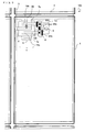
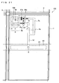
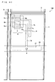
- Figures 1 through 3 are schematic plan views each showing a structure of a pixel in an active matrix substrate 100 according to First Embodiment.
- Figure 1 shows a structure of a pixel in which pixel defect correction is not carried out
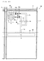
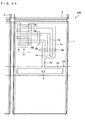
- Figures 2 and 3 show a structure of a pixel in which pixel defect has been corrected.
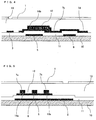
- Figure 4 is a cross-sectional view, taken along the line A1-A2 of Figure 1.
- Figure 5 is a cross-sectional view, taken along the line B1-B2 of Figure 1.
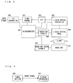
- Figure 6 is a structure view of a display apparatus including an active matrix substrate according to the present embodiment.
- Figure 7 shows a structure of a television image receiver including the display apparatus of Figure 6.
- a plurality of pixel electrodes 1 are arranged on an active matrix substrate 100 in matrix.
- the scanning signal lines 2 for supplying scanning signals and the data signal lines 3 for supplying data signals are provided.
- the scanning signal lines 2 and the data signal lines 3 intersect with each other.
- a TFT 4 is provided so as to serve as an active element (switching element).
- the TFT4 serving as an active element includes a gate electrode 5 connected to a scanning line 2 and a source electrode 6 connected to the data signal line 3, and drain electrodes 16a and 16b. Further, the drain electrodes 16a and 16b are connected to drain outgoing wires 7a, 7b and 7c serving as a first conductive pattern section made of a conductive layer constituting a wire section.
- the drain outgoing wire made up of an outgoing wire common section 7d and the drain outgoing wire branch sections 7a and 7b which respectively extend into the drain electrodes 16a and 16b.
- the drain outgoing wire common section 7d is connected to the pixel electrode 1 via a contact hole 8.
- the active matrix substrate according to the present embodiment further includes a correction connection electrode 9 (second conductive pattern section), which is partly (150 ⁇ m 2 ) overlapped with each of the outgoing wire branch sections 7a and 7b via the insulating layer.
- the correction connection electrode 9 is connectable to either or both of the branch section 7a and 7b, penetrating through the insulating layer.
- the correction connection electrode 9 does not serve as a wire section for connecting the drain electrodes 16a and 16b into the pixel electrode 1.
- the operation of the TFT 4 is controlled by scanning signals supplied to the gate electrode 5, and the pixel electrode 1 is supplied with an intended level of voltage as a data signal is supplied to the source electrode 6.
- Figure 4 is a cross-sectional view, taken along the line A1-A2 in the active matrix substrate shown in Figure 1.
- Figure 5 is a schematic cross-sectional view, taken along the line B1-B2 of Figure 1.
- a gate electrode 5 is connected to a scanning line 2 on a transparent insulating substrate 10, which is made of glass, plastic or the like.
- the scanning signal line 2 and the gate electrode 5 are formed from a metal film such as titanium, chrome, aluminum, molybdenum, tantalum, tungsten, copper, an alloy film of those, or a lamination film of those.
- a 1000 ⁇ - 3000 ⁇ thick film is deposited by sputtering or the like, and is patterned into a target shape by photoetching or the like.
- the correction connection electrode 9 is also formed in this process for forming the scanning signal line 2 and the gate electrode 5. By thus forming them in the same manufacturing process, the time and cost for manufacturing is reduced.
- the correction connection electrode 9 is formed to be overlapped with the drain outgoing wire branch section 7a and 7b, which are formed above the correction connection electrode 9 in a later process.
- the active matrix substrate of the present embodiment also includes a gate insulating film 11 which covers all of the scanning signal line 2, gate electrode 5 and correction connection electrode 9.
- the gate insulating film 11 is formed from an insulating film of silicon nitride, silicon oxide or the like.
- a high-resistance semiconductor layer 12 made of amorphous silicon, polysilicon etc. is formed to be overlapped with the gate electrode 5.
- a low-resistance semiconductor layer is formed as an ohmic contact layer.
- the low-resistance semiconductor layer is formed from n+ amorphous silicon or the like doped with phosphor, and is formed into the source electrode 6 and the drain electrodes 16a and 16b.
- the gate insulating film 11 made of silicon nitride, silicon oxide etc., a high-resistance semiconductor layer 12 made of amorphous silicon or the like, the low-resistance semiconductor layers 6, 16a and 16b made of n+ amorphous silicon or the like are all deposited by plasma CVD (chemical vapor deposition), and are pattern into corresponding shapes by photoetching or the like.
- the thicknesses of the silicon nitride film to be the gate insulating film 11, the amorphous silicon film to be the high-resistance semiconductor layer 12, and the n+ amorphous silicon film to be the low-resistance semiconductor layers 6, 16a and 16b are about 3000 ⁇ - 5000 ⁇ , 1000 ⁇ - 3000 ⁇ and 400 ⁇ - 700 ⁇ , respectively.
- the data signal line 3, the drain outgoing wire branch sections 7a and 7b, and the drain outgoing wire common section 7d are all formed in the same manufacturing process.
- the data signal line 3, the drain outgoing wire branch sections 7a and 7b, and the drain outgoing wire common section 7d are formed from a metal film such as titanium, chrome, aluminum, molybdenum, tantalum, tungsten, copper, an alloy film of those, or a lamination film of those.
- a 1000 ⁇ - 3000 ⁇ thick film is deposited by sputtering or the like, and is patterned into a target shape by photoetching or the like.
- the high-resistance semiconductor layer 12 made of amorphous silicon or the like, and the low-resistance semiconductor layers 6, 16a and 16b made of n+ amorphous silicon or the like are subjected to channel etching by way of dry etching, using the patterns of the data signal line 3 and the drain outgoing wire branch section 7a and 7b as masks.
- the TFT is thus completed.
- the active matrix substrate according to the present embodiment includes an interlayer insulating film 13, which is made of a resin film made of photosensitive acrylic resin or the like, an inorganic insulating film made of silicon nitride, silicon oxide etc., or a lamination film of those.
- the lamination film may be made by overlaying a 20000 ⁇ - 40000 ⁇ thick photosensitive acrylic resin film on an about 2000 ⁇ - 5000 ⁇ thick silicon nitride film deposited by CVD or the like, by way of die-coating.
- the contact hole is so formed as to penetrate through the interlayer insulating film 13 which is layered on the TFT, the scanning signal line 2, the data signal line 3, the drain outgoing wire branch sections 7a and 7b, and the drain outgoing wire common section 7d.
- the contact hole is formed by patterning a photosensitive acrylic resin by photolithography (exposure and development), for example.
- the pixel electrode 1 is formed above the interlayer insulating film 13.
- One example of formation of pixel electrode 1 is depositing an about 1000 ⁇ - 2000 ⁇ thick transparent conductive film from ITO, IZO, zinc oxide, tin oxide etc. by sputtering or the like, and then patterning the conductive film into a target shape by photoetching or the like.
- Figure 2 shows a pixel which has been through defect correction to solve a defect (such as leak) in the drain electrode 16a due to the residue film defect 99 between the source electrode 6 and the drain electrode 16a.
- the pixel defect was corrected by cutting the portion 97a of the drain outgoing wire branch section 7a.
- the portion 97a resides between the drain outgoing wire common section 7d and a portion where the drain outgoing wire branch section 7a is overlapped with the correction connection electrode 9.
- This pixel defect correction can be carried out by finding out, prior to cutting the branch section, whether the defect exists in the drain electrode 16a or in the drain electrode 16b by the appearance test. Also, in the case where it is already known, by an electric testing or the like, that the defect exists at least either of the drain electrode 16a or the drain electrode 16b, one of the branch sections is cut and another electric testing is performed. If the pixel defect is solved by the cutting, the resulting pixel will look like one in Figure 2. In this case, the drain outgoing wire branch section 7a is cut at the portion 97a which resides between the drain outgoing wire common section 7d and a portion where the drain outgoing wire branch section 7a is overlapped with the correction connection electrode 9.
- the drain electrode 16a is blocked from electricity, and the drain electrode 16b is connected to the outgoing wire common section 7d via the outgoing wire branch section 7b, and the drain outgoing wire common section 7d is connected to the pixel electrode 1 via the contact hole 8.
- the correction connection electrode 9 does not serve as a wire for connecting the drain electrode 16b to the pixel electrode 1.
- Figure 3 shows a pixel which has been through defect correction to solve a defect (such as leak) in the drain electrode 16b due to the residue film defect 99 between the source electrode 6 and the drain electrode 16b.
- the pixel defect was corrected by cutting the portion 97a of the drain outgoing wire branch section 7a and the portion 97b of the drain outgoing wire branch section 7b.
- the portion 97a resides between the drain outgoing wire common section 7d and a portion where the drain outgoing wire branch section 7a is overlapped with the correction connection electrode 9, and the portion 97b resides between the drain electrode 16b and a portion where the drain outgoing wire branch section 7b is overlapped with the correction connection electrode 9.
- both of the drain outgoing wire branch sections 7a and 7b are electrically connected to the correction connection electrode 9 through the insulating layer at the portion 96a.
- This pixel defect correction is performed in the following case. It is already known, by an electric testing or the like, that the defect exists at least either of the drain electrode 16a or the drain electrode 16b, and one of the branch sections is cut. However, according to the subsequent electric testing, the defect was not corrected. In this case, it can be assumed that the defect does not exist in the drain electrode having been cut. Therefore, the conduction between the common section and the branch section having been cut is recovered through the correction connection electrode. Then the other branch section is cut.
- the drain electrode 16b is blocked from electricity, and the drain electrode 16a is connected to the drain outgoing wire common section 7d via the drain outgoing wire branch section 7a, the correction connection electrode 9 and the drain outgoing wire branch section 7b, through the alternative path 95. Then, the drain outgoing wire common section 7d is connected to the pixel electrode 1 via the contact hole 8.
- the drain outgoing wire branch section is divided by breaking the cut-off sections 97a and 97b with laser beam irradiation.
- the laser beam is emitted to the cut-off sections 97a and 97b through either the front or rear surface of the substrate.
- the conduction portion 96a is irradiated with a laser beam through either the front or rear surface of the substrate.
- the pattern shape of the correction connection electrode 9 is rectangular (quadrangle) as shown in Figures 1 through 3.
- the pattern shape of the correction connection electrode 9 is not limited to this, and may be a triangle, a hemicycle or a trapezoid. More specifically, it is preferable that a part of the correction connection electrode 9 be so formed as to overlap the patterns of the drain outgoing wire branch section 7a and 7b via a gate insulating film, and ensure a portion to be subjected to laser irradiation.
- an alternative path such as 95 in Figure 3 is preferably provided.
- the location of the portion where the correction connection electrode and the drain outgoing wire branch section are overlapped is not particularly limited.
- the pixel defect correction according to the present embodiment is basically performed after at least a pixel electrode is formed.
- the correction is preferably carried out after the active matrix substrate is bonded with a color filter substrate, and liquid crystal is injected and sealed in the substrate to complete a panel.
- the timing of correction is not strictly limited to this, and the present embodiment also includes a correction carried out after the channel etching, which is performed after the drain outgoing wires 7a, 7b, and 7d are formed.
- Figure 6 shows a circuit block of a liquid crystal display apparatus.
- the reference numeral 500 denotes a Y/C separation circuit.
- 501 denotes a video chroma circuit
- 502 denotes a A/D converter
- 503 denotes a liquid crystal controller
- 504 denotes a liquid crystal panel
- 505 denotes a backlight drive circuit
- 506 denotes a backlight
- 507 denotes a microcomputer
- 508 denotes a gradation circuit.
- the liquid crystal panel is constituted of the active matrix substrate according to the present embodiment.
- An input image signal of television signal is supplied to the Y/C separation circuit 500 so as to be broken into a luminance signal and a color signal.
- the luminance signal and a color signal are converted into three primary colors R, G and B in the video chroma circuit 501.
- the analog signal is further converted into a digital signal in the A/D converter 502, before supplied to the liquid crystal controller 503.
- the liquid crystal panel 504 is supplied with RGB signals from the liquid crystal controller 503 at predetermined timings, and also is supplied with respective voltages of R, G and B from the gradation circuit 508. As a result, an image is displayed. Including these processes, the control of the entire system is carried out by the microcomputer 507.
- Such image display may be carried out in accordance with various video signals, such as video signals of television broadcast, video signals captured by a camera, or video signals supplied through the Internet lines.
- the tuner section 600 shown in Figure 7 receives a television broadcast and outputs video signals, and the display apparatus 601 carries out image (video picture) display in accordance with the video signals transmitted from the tuner section 600.
- the liquid crystal display apparatus shown in Figure 6 may be used as the display apparatus.
- the display apparatus may also be realized by other types of display apparatus such as an organic EL display apparatus.
- the display apparatus and the television image-receiver according to the present embodiment may also be constituted of the respective active matrix substrates described in the following Second to Fourth Embodiments.
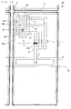
- Figures 8 through 10 are schematic plan views showing a structure of a pixel in an active matrix substrate 100 according to Second Embodiment.
- Figure 8 shows a structure of a pixel in which a pixel defect is not corrected.
- Figures 9 and 10 show a structure of a pixel having been subjected to pixel defect correction.
- the active matrix substrate 100 includes a plurality of pixel electrodes 1 arranged in matrix, in the vicinity of the pixel electrodes 1, the scanning signal lines 2 for supplying scanning signals and the data signal lines 3 for supplying data signals are provided.
- the scanning signal lines 2 and the data signal lines 3 intersect with each other.
- a TFT 4 is provided so as to serve as an active element (active element).
- the TFT4 serving as an active element includes a gate electrode 5 connected to a scanning line 2 and a source electrode 6 connected to the data signal line 3, and drain electrodes 16a and 16b.
- the drain electrodes 16a and 16b are connected to the drain outgoing wires 7a, 7b, and 7d (first conductive pattern section) made of a conductive layer constituting a wire section.
- the drain outgoing wire made up of an outgoing wire common section 7d and the drain outgoing wire branch sections 7a and 7b which respectively extend into the drain electrodes 16a and 16b.
- the drain outgoing wire common section 7d is connected to the pixel electrode 1 via a contact hole 8 and one of the electrodes (retention capacitor upper electrode) 21 of the retention capacitor element.
- the retention capacitor wire 22 serves as the other electrode (retention capacitor lower electrode) of the retention capacitor element.
- the active matrix substrate according to the present embodiment further includes a correction connection electrode 9, which is partly (150 ⁇ m 2 ) overlapped with each of the outgoing wire branch sections 7a and 7b via the insulating layer.
- the correction connection electrode 9 is connectable to either or both of the branch section 7a and 7b, penetrating through the insulating layer.
- the correction connection electrode 9 does not serve as a wire section for connecting the drain electrodes 16a and 16b into the pixel electrode 1.
- Figure 9 shows a pixel which has been through defect correction to solve a defect (such as leak) in the drain electrode 16a due to the residue film defect 99 between the source electrode 6 and the drain electrode 16a.
- the pixel defect was corrected by cutting the portion 97a of the drain outgoing wire branch section 7a.
- the portion 97a resides between the drain outgoing wire common section 7d and a portion where the drain outgoing wire branch section 7a is overlapped with the correction connection electrode 9.
- This pixel defect correction can be carried out by finding out, prior to cutting the branch section, whether the defect exists in the drain electrode 16a or in the drain electrode 16b by the appearance test. Also, in the case where it is already known, by an electric testing or the like, that the defect exists at least either of the drain electrode 16a or the drain electrode 16b, one of the branch sections is cut and another electric testing is performed. If the pixel defect is solved by the cutting, the resulting pixel will look like one in Figure 9. In this case, the drain outgoing wire branch section 7a is cut at the portion 97a which resides between the drain outgoing wire common section 7d and a portion where the drain outgoing wire branch section 7a is overlapped with the correction connection electrode 9.
- the drain electrode 16a is blocked from electricity, and the drain electrode 16b is connected to the outgoing wire common section 7d via the outgoing wire branch section 7b, and the drain outgoing wire common section 7d is connected to the pixel electrode 1 via the contact hole 8.
- the correction connection electrode 9 does not serve as a wire for connecting the drain electrode 16b to the pixel electrode 1.
- Figure 10 shows a pixel which has been through defect correction to solve a defect (such as leak) in the drain electrode 16b due to the residue film defect 99 between the source electrode 6 and the drain electrode 16b.
- the pixel defect was corrected by cutting the portion 97a of the drain outgoing wire branch section 7a and the portion 97b of the drain outgoing wire branch section 7b.
- the portion 9.7a resides between the drain outgoing wire common section 7d and a portion where the drain outgoing wire branch section 7a is overlapped with the correction connection electrode 9, and the portion 97b resides between the drain electrode 16b and a portion where the drain outgoing wire branch section 7b is overlapped with the correction connection electrode 9.
- both of the drain outgoing wire branch sections 7a and 7b are electrically connected to the correction connection electrode 9 through the insulating layer at the portion 96a.
- This pixel defect correction is performed in the following case. It is already known, by an electric testing or the like, that the defect exists at least either of the drain electrode 16a or the drain electrode 16b, and one of the branch sections is cut. However, according to the subsequent electric testing, the defect was not corrected. In this case, it can be assumed that the defect does not exist in the drain electrode having been cut. Therefore, the conduction between the common section and the branch section having been cut is recovered through the correction connection electrode. Then the other branch section is cut.
- the drain electrode 16b is blocked from electricity, and the drain electrode 16a is connected to the drain outgoing wire common section 7d via the drain outgoing wire branch section 7a, the correction connection electrode 9 and the drain outgoing wire branch section 7b, through the alternative path 95. Then, the drain outgoing wire common section 7d is connected to the pixel electrode 1 via the contact hole 8 and one of the electrodes (retention capacitor upper electrode) 21 of the retention capacitor element.
- the drain outgoing wire branch section is divided by breaking the cut-off sections 97a and 97b with laser beam irradiation.
- the laser beam is emitted to the cut-off sections 97a and 97b through either the front or rear surface of the substrate.
- the conduction portion 96a is irradiated with a laser beam through either the front or rear surface of the substrate.
- the pattern shape of the correction connection electrode 9 is rectangular (quadrangle) as shown in Figures 8 through 10.
- the pattern shape of the correction connection electrode 9 is not limited to this, and may be a triangle, a hemicycle or a trapezoid. More specifically, it is preferable that a part of the correction connection electrode 9 be so formed as to overlap the patterns of the drain outgoing wire branch section 7a and 7b via a gate insulating film, and ensure a portion to be subjected to laser irradiation.
- an alternative path such as 95 in Figure 10 is preferably provided.
- the location of the portion where the correction connection electrode and the drain outgoing wire branch section are overlapped is not particularly limited.
- the pixel defect correction according to the present embodiment is basically performed after at least a pixel electrode is formed.
- the channel causing leak can be securely removed electrically, and an alternative path can be provided.
- the timing of correction is not strictly limited to this, and the present embodiment also includes a correction carried out after the channel etching, which is performed after the drain outgoing wires 7a, 7b, and 7d are formed.
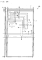
- Figures 11 through 14 are schematic plan views showing a structure of a pixel in an active matrix substrate 100 according to Third Embodiment.
- Figure 11 shows a structure of a pixel in which a pixel defect is not corrected.
- Figures 12, 13 and 14 show a structure of a pixel having been subjected to pixel defect correction.
- a single TFT includes two source electrodes 6a and 6b, and three drain electrodes 16a, 16b, and 16c.
- the source electrode 6a corresponds to the two drain electrodes 16a and 16b
- the source electrode 6b corresponds to two drain electrodes 16b and 16c.
- the active matrix substrate 100 includes a plurality of pixel electrodes 1 arranged in matrix, in the vicinity of the pixel electrodes 1, the scanning signal lines 2 for supplying scanning signals and the data signal lines 3 for supplying data signals are provided.
- the scanning signal lines 2 and the data signal lines 3 intersect with each other.
- a TFT 4 is provided so as to serve as an active element (switching element).
- the TFT4 serving as an active element includes a gate electrode 5 connected to a scanning line 2 and a source electrodes 6a and 6b connected to the data signal line 3, and drain electrodes 16a, 16b and 6c.
- the drain electrodes 16a, 16b and 16c are connected to the drain outgoing wires 7a, 7b, 7c and 7d (first conductive pattern section) made of a conductive layer constituting a wire section.
- the drain outgoing wire made up of an outgoing wire common section 7d and the drain outgoing wire branch sections 7a, 7b and 7c which respectively extend into the drain electrodes 16a, 16b and 16c.
- the drain outgoing wire common section 7d is connected to the pixel electrode 1 via a contact hole 8 and one of the electrodes (retention capacitor upper electrode) 21 of the retention capacitor element.
- the retention capacitor wire 22 serves as the other electrode (retention capacitor lower electrode) of the retention capacitor element.
- the active matrix substrate according to the present embodiment further includes a correction connection electrode 9, which is partly (150 ⁇ m 2 ) overlapped with each of the outgoing wire branch sections 7a, 7b and 7c via the insulating layer.
- the correction connection electrode 9 is connectable to either or both of the branch section 7a, 7b and 7c, penetrating through the insulating layer.
- the correction connection electrode 9 does not serve as a wire section for connecting the drain electrodes 16a 16b and 16c into the pixel electrode 1.
- Figure 12 shows a pixel which has been through defect correction to solve a defect (such as leak) in the drain electrode 16a due to the residue film defect 99 between the source electrode 6a and the drain electrode 16a.
- the pixel defect was corrected by cutting the portion 97a of the drain outgoing wire branch section 7a.
- the portion 97a resides between the drain outgoing wire common section 7d and a portion where the drain outgoing wire branch section 7a is overlapped with the correction connection electrode 9.
- This pixel defect correction can be carried out by finding out, prior to cutting the branch section, whether the defect exists in the drain electrode 16a, in the drain electrode 16b, or in the drain electrode 16c by the appearance test. Also, in the case where it is already known, by an electric testing or the like, that the defect exists at least one of the drain electrode 16a, the drain electrode 16b, or the drain electrode 16c, one of the branch sections is cut and another electric testing is performed. If the pixel defect is solved by the cutting, the resulting pixel will look like one in Figure 12. In this case, the drain outgoing wire branch section 7a is cut at the portion 97a which resides between the drain outgoing wire common section 7d and a portion where the drain outgoing wire branch section 7a is overlapped with the correction connection electrode 9.
- the drain electrode 16a is blocked from electricity, and the drain electrode 16b and 16c are connected to the outgoing wire common section 7d via the outgoing wire branch sections 7b and 7c, respectively; and the drain outgoing wire common section 7d is connected to the pixel electrode 1 via one of the electrodes (retention capacitor upper electrode) 21 of the retention capacitor element and the contact hole 8.
- the correction connection electrode 9 does not serve as a wire for connecting the drain electrodes 16b and 16c to the pixel electrode 1.
- Figure 13 shows a pixel which has been through defect correction to solve a defect (such as leak) in the drain electrode 16b due to the residue film defect 99 between the source electrode 6b and the drain electrode 16b.
- the pixel defect was corrected by cutting the portion 97a of the drain outgoing wire branch section 7a and the portion 97b of the drain outgoing wire branch section 7b.
- the portion 97a resides between the drain outgoing wire common section 7d and a portion where the drain outgoing wire branch section 7a is overlapped with the correction connection electrode 9, and the portion 97b resides between the drain outgoing wire branch section 7b and a portion where the drain outgoing wire branch section 7b is overlapped with the correction connection electrode 9.
- both of the drain outgoing wire branch sections 16a and 16c are electrically connected to the correction connection electrode 9 through the insulating layer at the portion 96a.
- This pixel defect correction is performed in the following case.
- the defective part cannot be found by the appearance test but it is already known, by an electric testing or the like, that the defect exists at least one of the drain electrode 16a, the drain electrode 16b, or the drain electrode 16c; and one of the branch sections is cut. However, according to the subsequent electric testing, the defect was not corrected. In this case, if the pixel defect is cleared away by cutting one of the two uncut branch sections, it can be assumed that the defect does not exist in the drain electrode having been cut first. Therefore, the conduction between the common section and the branch section having been cut first is recovered through the correction connection electrode. In the pixel of Figure 13, the pixel defect was not solved even after cutting the branch section 7a at the portion 97a. Then, the branch section 7b was cut at the portion 97b, which solved the pixel defect. Then, the connection between the branch section 7a and the branch section 7c are recovered through the correction connection electrode 9.
- the drain electrode 16b is blocked from electricity, and the drain electrode 16a is connected to the drain outgoing wire common section 7d via the drain outgoing wire branch section 7a, the correction connection electrode 9 and the drain outgoing wire branch section 7c, through the alternative path 95. Further, the drain electrode 16c is connected to the drain outgoing wire section 7d via the drain outgoing wire branch section 7c. Then, the drain outgoing wire common section 7d is connected to the pixel electrode 1 via the contact hole 8 and one of the electrodes (retention capacitor upper electrode) 21 of the retention capacitor element.
- Figure 14 shows a pixel which has been through defect correction to solve a defect (such as leak) in the drain electrode 16c due to the residue film defect 99 between the source electrode 6b and the drain electrode 16c.
- the pixel defect was corrected by cutting the portion 97a of the drain outgoing wire branch section 7a, the portion 97b of the drain outgoing wire branch section 7b, and the portion 97c of the drain outgoing wire branch section 7c.
- the portion 97a resides between the drain outgoing wire common section 7d and a portion where the drain outgoing wire branch section 7a is overlapped with the correction connection electrode 9
- the portion 97b resides between the drain outgoing wire branch section 7d and a portion where the drain outgoing wire branch section 7b is overlapped with the correction connection electrode 9
- the portion 97c resides between the drain electrode 16c and a portion where the drain outgoing wire branch section 7c is overlapped with the correction connection electrode 9. Then all of the drain outgoing wire branch sections 16a, 16b and 16c are electrically connected to the correction connection electrode 9 through the insulating layer at the portion 96a.
- This pixel defect correction is performed in the following case.
- the defective part cannot be found by the appearance test but it is already known, by an electric testing or the like, that the defect exists at least one of the drain electrode 16a, the drain electrode 16b, or the drain electrode 16c; and two of the branch sections is cut. However, according to the subsequent electric testing, the defect was not corrected. In this case, if the pixel defect is not cleared away even after cutting one of the two uncut branch sections, it can be assumed that the defect does not exist in the two drain electrodes corresponding to the branch sections having been cut. Therefore, the conduction between the common section and the two branch sections having been cut first are recovered through the correction connection electrode. Then the remaining branch section is cut.
- the pixel defect was not solved even after cutting the branch sections 7a at the portion 97a and subsequently cutting 7b at the portion 97b. Then, the connection between the branch sections 7a, 7b and 7c are recovered through the correction connection electrode 9. The branch sections 7c is cut at the portion 97c.
- the drain electrode 16c is blocked from electricity, and the drain electrode 16a is connected to the drain outgoing wire common section 7d via the drain outgoing wire branch section 7a, the correction connection electrode 9 and the drain outgoing wire branch section 7c, through the alternative path 95.
- the drain electrode 16b is connected to the drain outgoing wire common section 7d via the drain outgoing wire branch section 7b, the correction connection electrode 9 and the drain outgoing wire branch section 7c, through the alternative path 95.
- the drain outgoing wire common section 7d is connected to the pixel electrode 1 via the contact hole 8 and one of the electrodes (retention capacitor upper electrode) 21 of the retention capacitor element.
- the drain outgoing wire branch section is divided by breaking the cut-off sections 97a, 97b and 97c with laser beam irradiation.
- the laser beam is emitted to the cut-off sections 97a, 97b and 97c through either the front or rear surface of the substrate.
- the conduction portion 96a is irradiated with a laser beam through either the front or rear surface of the substrate.
- the pattern shape of the correction connection electrode 9 is rectangular (quadrangle) as shown in Figures 11 through 14.
- the pattern shape of the correction connection electrode 9 is not limited to this, and may be a triangle, a hemicycle or a trapezoid. More specifically, it is preferable that a part of the correction connection electrode 9 be so formed as to overlap the patterns of the drain outgoing wire branch section 7a, 7b and 7c via a gate insulating film, and ensure a portion to be subjected to laser irradiation.
- an alternative path such as 95 in Figures 13 and 14 is preferably provided.
- the location of the portion where the correction connection electrode and the drain outgoing wire branch section are overlapped is not particularly limited.
- the pixel defect correction according to the present embodiment is basically performed after at least a pixel electrode is formed. However, in applying this method to a liquid crystal display apparatus, it is more preferable to carry out the correction after the liquid crystal layer is formed so as to confirm lighting of panel. In this way, the channel causing leak can be securely removed electrically, and an alternative path can be provided.
- the timing of correction is not strictly limited to this, and the present embodiment also includes a correction carried out after the channel etching, which is performed after the drain outgoing wires 7a, 7b, 7c and 7d are formed.
- the present embodiment uses a TFT containing three drain electrodes, the present invention is not limited to this structure.
- the pixel defect correction according to the present invention may be performed in the same manner for a TFT containing 4 or more drain electrodes.
- Figure 15 shows a schematic plan view showing a structure of a pixel in an active matrix substrate 100 according to Fourth Embodiment.
- Figure 15 shows a structure of a pixel in which a pixel defect is not corrected.
- Figures 16 and 17 show a structure of a pixel having been subjected to pixel defect correction.
- the active matrix substrate As shown in Figures 15 through 17, in the active matrix substrate according to the present embodiment, the pixel is broken into a plurality of pixels, and sub-pixel electrode 1a and 1b are respectively connected to separate TFT 4a and 4b.
- the active matrix substrate of the present invention has so-called a multi pixel structure.
- the active matrix substrate 100 includes a plurality of sub-pixel electrodes 1a and 1b arranged in matrix, in the vicinity of the sub-pixel electrodes 1a and 1b, the scanning signal lines 2 for supplying scanning signals and the data signal lines 3 for supplying data signals are provided.
- the scanning signal lines 2 and the data signal lines 3 intersect with each other.
- TFT 4a and 4b are provided so as to serve as a switching element.
- These TFT 4a and 4b each have an on GATE (TFT on gate) structure, and the scanning signal line 2 serves also as a gate electrode. This arrangement gives an effect of increase of aperture ratio.
- the TFT 4a and 4b serving as active elements each include a gate electrode and a source electrode 6 connected to the data signal line 3, and drain electrodes 16a and 16b.
- the drain electrodes 16a and 16b are connected to the drain outgoing wires 7a, 7b and 7d (first conductive pattern section) made of a conductive layer constituting a wire section.
- the drain outgoing wire made up of an outgoing wire common section 7d and the drain outgoing wire branch sections 7a and 7b which respectively extend into the drain electrodes 16a and 16b.
- the drain outgoing wire common section 7d is connected to the sub-pixel electrodes 1a and 1b via a contact hole 8 and one of the electrodes (retention capacitor upper electrode) 21 of the retention capacitor element.
- the retention capacitor wire 22 serves as the other electrode (retention capacitor lower electrode) of the retention capacitor element.
- the active matrix substrate according to the present embodiment further includes an electrode 9a, which is partly (150 ⁇ m 2 ) overlapped with each of the outgoing wire branch sections 7a and 7b via the insulating layer.
- the electrode 9a is connectable to either or both of the branch section 7a and 7b, penetrating through the insulating layer.
- the electrode 9a connected to the retention capacitor wire 22 is so provided as to overlap with the (sub-) pixel electrode slit 30 of the active matrix substrate.
- the pixel electrode slit 30 of the active matrix substrate is an electrode pattern for controlling division/alignment of liquid crystal.
- the pixel electrode slit 30 is formed on a substrate in a vertical alignment-type liquid crystal display apparatus of MVA mode, typically used for a large-sized liquid crystal TV.
- the electrode 9a (an extension part of the retention capacitor wire 22, and may serve as a correction connection electrode) different in potential from the pixel electrode is provided under pixel electrode slit 30.
- the fringe field effect in the pixel electrode slit 30 appears more effectively, and the alignment control effect of liquid crystal increases.
- a part of the electrode 9a may be electrically separated from at least one of the retention capacitor wires 22 in the same conductive layer to be serve as a correction connection electrode.
- the electrode 9a is formed under the pixel electrode slit 30 which does not affect the aperture ratio, it is possible to maintain the aperture ratio.
- the electrode 9a extended from the retention capacitor wire 22 is provided to overlap with the (sub-) pixel electrode slit 30 of the active matrix substrate.
- the pixel electrode slit 30 of the active matrix substrate is an electrode pattern for controlling division/alignment of liquid crystal.
- the pixel electrode slit 30 is formed on a substrate in a vertical alignment-type liquid crystal display apparatus of MVA mode, typically used for a large-sized liquid crystal TV.
- the pattern shape of the electrode 9a is not limited to those shown in Figures 15 through 17.
- the shape of the electrode 9a is adjustable according to the shape of the pixel electrode slit 30 and the pattern of the capacitor wire 22.
- the electrode pattern 9a it is not necessary to place all of the electrode pattern 9a.
- the electrode (an extension part of the retention capacitor wire) is overlapped with the slit electrode pattern for controlling division/ alignment of liquid crystal formed on a substrate in a vertical alignment type liquid crystal display apparatus of MVA mode.
- the present invention is not limited to this case.
- the electrode may be overlapped with a projection for controlling division/alignment of liquid crystal formed on a substrate. This layout also has the effect of ensuring the aperture ratio.
- the operation of the TFT 4a and 4b are controlled by scanning signals supplied to the gate electrode 5, and the sub-pixel electrodes 1a and 1b are supplied with intended levels of voltage as data signals are supplied to the source electrode 6 of the TFT 4a and 4b.
- the retention capacitor wires 22 which individually serve as the retention capacitor lower electrodes for the respective sub-pixels are supplied with plural signals with different phases (pixel division method).
- the signals supplied to these retention capacitor lower electrodes vary the respective luminances of the plural sub-pixels constituting a pixel. This gives an effect of increase of the viewing angle characteristic (i.e., it suppresses excess brightness in the oblique viewing angle).
- the correction connection electrode 9a does not serve as a wire section for connecting the drain electrodes 16a and 16b into the pixel electrode 1. Further, since the electrode. 9a is not required to function as a wire section, the part of the electrode 9a which can be used as a correction connection electrode is not electrically separated from the retention capacitor wire 22.
- Figure 16 shows a pixel of the TFT 4b connected to the sub-pixel 1b.
- This pixel has been through defect correction to solve a defect (such as leak) in the drain electrode 16a due to the residue film defect 99 between the source electrode 6 and the drain electrode 16a.
- the pixel defect was corrected by cutting the portion 97a of the drain outgoing wire branch section 7a.
- the portion 97a resides between the drain outgoing wire common section 7d and a portion where the drain outgoing wire branch section 7a is overlapped with the electrode 9a.
- This pixel defect correction can be carried out by finding out, prior to cutting the branch section, whether the defect exists in the drain electrode 16a or in the drain electrode 16b by the appearance test. Also, in the case where it is already known, by an electric testing or the like, that the defect exists at least either of the drain electrode 16a or the drain electrode 16b, one of the branch sections is cut and another electric testing is performed. If the pixel defect is solved by the cutting, the resulting pixel will look like one in Figure 16. In this case, the drain outgoing wire branch section 7a is cut at the portion 97a which resides between the drain outgoing wire common section 7d and a portion where the drain outgoing wire branch section 7a is overlapped with the correction connection electrode 9a.
- the drain electrode 16a is blocked from electricity, and the drain electrode 16b is connected to the outgoing wire common section 7d via the outgoing wire branch section 7b, and the drain outgoing wire common section 7d is connected to the pixel electrode 1 via the contact hole 8.
- the electrode 9 does not serve as a wire section for connecting the drain electrode 16b into the sub-pixel electrode 1b.
- the electrode 9a is not required to function as a wire section, the part of the electrode 9a which can be used as a correction connection electrode is not electrically separated from the retention capacitor wire 22.
- Figure 17 shows a pixel of the TFT 4b connected to the sub-pixel 1b.
- This pixel has been through defect correction to solve a defect (such as leak) in the drain electrode 16b due to the residue film defect 99 between the source electrode 6 and the drain electrode 16b.
- the pixel defect was corrected by cutting the portion 97a of the drain outgoing wire branch section 7a and the portion 97b of the drain outgoing wire branch section 7b.
- the portion 97a resides between the drain outgoing wire common section 7d and a portion where the drain outgoing wire branch section 7a is overlapped with the correction connection electrode 9a
- the portion 97b resides between the drain electrode 16b and a portion where the drain outgoing wire branch section 7b is overlapped with the correction connection electrode 9a.
- both of the drain outgoing wire branch sections 16a and 16b are electrically connected to the correction connection electrode 9a through the insulating layer at the portion 96a.
- This pixel defect correction is performed in the following case.
- the defective part cannot be found by the appearance test but it is already known, by an electric testing or the like, that the defect exists at least either of the drain electrode 16a or the drain electrode 16b, and one of the branch sections is cut. However, according to the subsequent electric testing, the defect was not corrected. In this case, it can be assumed that the defect does not exist in the drain electrode having been cut. Therefore, the conduction between the common section and the branch section having been cut is recovered through the correction connection electrode. Then the other branch section is cut.
- the drain electrode 16b is blocked from electricity, and the drain electrode 16a is connected to the drain outgoing wire common section via the drain outgoing wire branch section 7a, the correction connection electrode 9a and the drain outgoing wire branch section 7b, through the alternative path 95. Then, the drain outgoing wire common section 7d is connected to the sub-pixel electrode 1b via the contact hole 8 and one of the electrodes (retention capacitor upper electrode) 21 of the retention capacitor element.
- the drain outgoing wire branch section is divided by breaking the cut-off sections 97a, 97b and 120 with laser beam irradiation.
- the laser beam is emitted to the cut-off section 97a, 97b and 120 through either the front or rear surface of the substrate.
- the conduction portion 96a is irradiated with a laser beam through either the front or rear surface of the substrate.
- the described invention which enables pixel correction within the defective pixel has an effect of suppressing deterioration of the function of a sub-pixel with a different luminance. Therefore, the invention ensures superior viewing angle characteristic of multi pixel driving.
- the present embodiment describes a case where the sub-pixel 1b has the pixel defect.
- the invention may also be useful to correct defects in the sub-pixel 1a.
- the present embodiment describes a case of multi-pixel structure in which a single pixel is constituted of two sub-pixels, the case where the pixel is constituted of three or more pixels falls also within the scope of the invention.
- the present embodiment describes a case of multi-pixel structure of MVA mode, but the scope of invention also includes a MVA mode not using multi-pixel structure, or a multi-pixel structure of a mode other than MVA.
- the described invention is not limitedly used for a liquid crystal display apparatus, and may be adopted for other types of display apparatuses.
- it may be used for an organic EL display with the following manner.
- the active matrix substrate according to the present invention is placed opposite to a color filter substrate, and an organic EL layer is provided between the two substrates to form an organic EL panel, which is completed as an organic EL display apparatus by connecting into a driver or the like via an external connection terminal.
- the present invention is applicable to any kinds of display apparatus other than a liquid crystal display apparatus or an organic EL display apparatus, as long as the display apparatus uses an active matrix substrate.
- the active matrix substrate according to the present embodiment is the same as those described in Second and Third embodiments with reference to Figures 8 and 11, except that in the present embodiment the TFT (active element) 4 includes a plurality of correction connection electrodes 9.
- the active matrix substrate 100 includes the same drain electrodes 16a and 16b as those shown in Figure 8 of Second Embodiment. As with Second Embodiment, the drain electrodes 16a and 16b are connected to the drain outgoing wire branch section 7a and 7b, and the drain outgoing wire common section 7d is connected to the pixel electrode 1 via the contact hole 8.
- the active matrix substrate 100 shown in Figure 8 includes a single correction connection electrode 9 which serves as the second conductive pattern section and is provided in the vicinity of the drain outgoing wire common section 7d across the drain outgoing wire branch sections 7a and 7b.
- the active matrix substrate 100 of Figure 19 includes two correction connection electrodes 9a and 9b, near the drain outgoing wire common section 7d and near the TFT 4, respectively. The two correction connection electrodes 9a and 9b are provided across the drain outgoing wire branch section 7a and 7b.
- the active matrix substrate 100 shown in Figure 20 corresponds to the active matrix substrate 100 of Figure 11 according to Third Embodiment in which the drain electrodes 16a, 16b and 16c are connected to the drain outgoing wire branch sections 7a, 7b and 7c; and the drain outgoing wire common section 7d is connected to the pixel electrode 1 via the contact hole 8.
- the active matrix substrate 100 shown in Figure 11 includes a single correction connection electrode 9 which serves as the second conductive pattern section and is provided in the vicinity of the drain outgoing wire common section 7d across the drain outgoing wire branch sections 7a, 7b and 7c.
- the active matrix substrate 100 of Figure 20 includes two correction connection electrodes 9a and 9b, near the drain outgoing wire common section 7d and near the TFT 4, respectively. The two correction connection electrodes 9a and 9b are provided across the drain outgoing wire branch section 7a, 7b and 7c.
- This structure in which a plurality of correction connection electrodes 9 are provided for a single TFT4 has an effect of increasing security of pixel defect correction.
- the pixel correct defection cannot be performed if the drain outgoing wire branch section 7a (or 7b) is cut off as shown by the numeral 80 of Figure 21, or if the correction connection electrode 9a itself is cut off as shown by the numeral 81 of Figure 22.
- the pixel defect correction can be performed with the correction connection electrode 9b even if the drain outgoing wire branch section 7a (or 7b) is cut off as shown by the numeral 80 of Figure 21, or if the correction connection electrode 9a is cut off as shown by the numeral 81 of Figure 22.
- the gap between the correction connection electrodes 9a and 9b is preferably large. Therefore, as shown in Figures 19 and 20, the correction connection electrodes 9a and 9b are preferably provided near the drain outgoing wire common section 7d and near the TFT 4, respectively. If both of the correction connection electrodes 9a and 9b are provided near the TFT 4, the pixel defect cannot be corrected when the drain outgoing wire branch section 7a (or 7b) is cut off as shown by the numeral 80 of Figure 21.
- the number of correction connection electrodes 9 is determined in consideration of aperture ratio and probability of occurrence of line breakage 80/81.
- each of the active matrix substrates 100 shown in Figures 23 and 24 includes three drain electrodes 16a 16b and 16c, and two correction connection electrodes 9.
- the active matrix substrate 100 includes two correction connection electrodes 9a and 9b, which are provided across the all of the three drain outgoing wire branch section 7a, 7b and 7c (second conductive pattern A section).
- the correction connection electrode 9a which is one of the two correction connection electrodes, run across all of the drain outgoing wire branch sections 7a, 7b and 7c.
- the correction connection electrode 9B runs across a part of the three drain outgoing wire branch section, more specifically, it runs across two out of the three drain outgoing wires (second conductive pattern B section).
- the correction connection electrode 9B runs across drain outgoing wire branch sections 7a and 7b.
- the correction connection electrode 9B runs across the drain outgoing wire branch sections 7b and 7c.
- the correction connection electrode 9B which enables conduction of a part of the plural drain outgoing wire branch sections is provided. This maintains a certain redundant effect, and ensures high aperture ratio.
- the correction connection electrode 9B which enables conduction of a part of the plural drain outgoing wire branch sections, it is preferable that the correction connection electrode 9B be partly overlapped with the longest drain outgoing wire branch section out of the three drain outgoing wire branch sections, and the longest drain outgoing wire branch section be made conductible to the other drain outgoing wire branch sections.
- the drain outgoing wire branch section 7c is most likely to break. That is, the active matrix substrate 100 of Figure 24 in which the correction connection electrode 9B runs across the longest drain outgoing wire branch section 7c and the drain outgoing wire branch section 7b more securely ensures pixel defect correction than the active matrix substrate 100 of Figure 23.
- the active matrix substrate 100 of the present embodiment is the same as the active matrix substrate 100 of Figure 8 of Second Embodiment, except that the pixel electrode 1 includes a removal section 83 which is a portion where ITO, which is the material of pixel electrode, is removed.
- the removal section 83 is partly overlapped with the drain outgoing wire branch sections 7a and 7b.
- the pixel electrode 1 includes a removal section 83 which is a portion where ITO, which is the material of pixel electrode, is removed, and is partly overlapped with the drain outgoing wire branch sections 7a and 7b.
- the removal section 83 is provided corresponding to the correction connection electrode 9. With this layout, it is possible to prevent the leak between the pixel electrode 1 and the drain outgoing wire branch section 7a (or 7b) connected to the SD leak channel when the drain outgoing wire branch section 7a or 7b are connected to the correction connection electrode 9.
- the removal section 83 is provided corresponding to the cutting portion of the drain outgoing wire branch section 7a or 7b. With this arrangement, it is possible to prevent the leak between the pixel electrode 1 and the drain outgoing wire branch section 7a (or 7b) connected to the SD leak channel when the drain outgoing wire branch section 7a or 7b is cut.
- the removal section 83 is positioned corresponding to the correction connection electrode 9 and the drain outgoing wire branch sections 7a and 7b. With this arrangement, it is possible to prevent the leak between the pixel electrode 1 and the drain outgoing wire branch section 7a (or 7b) connected to the SD leak channel when the drain outgoing wire branch section 7a or 7b are connected to the correction connection electrode 9, or when the drain outgoing wire branch section 7a or 7b is cut.
- the removal section 83 may be so constituted as to be a part of the liquid crystal molecule alignment control electrode slit 30 of the pixel electrode 1. As explained in Forth Embodiment, the region where the alignment control electrode slit 30 is formed does not normally function as a transmission region (opening section) in the liquid crystal display apparatus. By thus using the alignment control electrode slit 30 as the removal section 83, provision of removal section 83 does not decrease the aperture ratio.
- Figure 28 shows a structure of an active matrix substrate in which the alignment control electrode slit 30 functions as the removal section 83.
- the alignment control electrode slit 30 serves as the removal section 83, and the laser irradiation sections 97a and 97b are inclined along the slit.
- the removal section 83 disturbs the alignment of liquid crystal molecules, it is preferable to provide a light-shielding film 84 for blocking the removal section 83 from light, as shown in Figure 29.
- the color filter substrate which is provided as a counter substrate opposed to the active matrix substrate 100, is blocked from light by a black matrix. It is also allowable to provide the light-shielding film 84 on the active matrix substrate 100 as long as the light-shielding film 84 blocks the removal section 83 from light when viewed as a display apparatus from the vertical direction of the substrate (liquid crystal panel).
- the active matrix substrate 100 according to the present embodiment is the same as the active matrix substrate 100 of Figure 8 of Second Embodiment, except for the number of source electrodes 6.
- the active matrix substrate 100 of Figure 8 includes two (plural) drain electrodes for a single source electrode 6.
- the active matrix substrate of Figure 8 has two channels.
- the active matrix substrate 100 of the present embodiment includes three source electrodes 6a, 6b and 6c.
- the source electrodes 6a and 6b correspond to the drain electrode 16a
- the source electrode 6b and 6c correspond to the drain electrode 16b.
- the active matrix substrate 100 of Figure 30 has four channels.
- An active matrix substrate including plural drain electrodes for a single source electrode such as the active matrix substrate 100 of Figure 8 including two drain electrodes 16a and 16b for a single source electrode 6, ensures effects of high-speed display response and reduction of power consumption.
- the active matrix substrate 100 of Figure 30 does not ensure these effects.
- the active matrix substrate 100 of Figure 30 with the two drain outgoing wire branch sections 7a and 7b has the same number (three) of channels as those of the active matrix 100 of Figure 11 having three drain outgoing wire branch section 7a, 7b and 7c.
- the active matrix substrate of the present embodiment ensures the number of channels and also prevents decrease of pixel potential by the parasitic capacitor (Cgd) between the source electrode and the drain electrode of the TFT 4. On this account, it is possible to decrease the source voltage which increases the pixel electrode 1 to a desired effective voltage. As a result, the entire power consumption is reduced.
- Embodiments 1 through 7 may be freely combined.
- the embodiment in which a plurality of correction connection electrodes is provided for a single TFT may have a removal section.
- the embodiment in which a plurality of correction connection electrodes is provided for a single TFT may be combined with another embodiment in which a plurality of source electrodes are provided for a single drain electrode, which ensures the number of channels and also reduces power consumption.
- the active matrix substrate according to the present invention gives an effect of increase of yield of display apparatus.
- the active matrix substrate of the present invention is particularly useful for a componential member of a large-sized TV which requires effective prevention of point defect.
- the present invention is not limitedly used for a liquid crystal display apparatus, and may be adopted for other types of display apparatuses.
- it may be used for an organic EL display with the following manner.
- the active matrix substrate according to the present invention is placed opposite to a color filter substrate, and an organic EL layer is provided between the two substrates to form an organic EL panel, which is completed as an organic EL display apparatus by connecting into a driver or the like via an external connection terminal.
- the present invention is applicable to any kinds of display apparatus other than a liquid crystal display apparatus or an organic EL display apparatus, as long as the display apparatus uses an active matrix substrate.
Landscapes
- Physics & Mathematics (AREA)
- Nonlinear Science (AREA)
- Engineering & Computer Science (AREA)
- Microelectronics & Electronic Packaging (AREA)
- Mathematical Physics (AREA)
- Chemical & Material Sciences (AREA)
- Crystallography & Structural Chemistry (AREA)
- General Physics & Mathematics (AREA)
- Optics & Photonics (AREA)
- Liquid Crystal (AREA)
- Thin Film Transistor (AREA)
- Devices For Indicating Variable Information By Combining Individual Elements (AREA)
Abstract
Description
- The present invention relates to an active matrix substrate for various display apparatuses, such as a liquid crystal display apparatus, EL (Electro Luminescence) display apparatus etc. More specifically, the present invention relates to an active matrix substrate suitable for a liquid crystal display apparatus with a large liquid crystal display screen, such as a large-size liquid crystal television.
- An active matrix substrate is widely used for various active matrix display apparatuses such as a liquid crystal display apparatus, an EL (Electro Luminescence) display apparatus etc. In an active matrix substrate used for a conventional active matrix liquid crystal display apparatus, a switching element such as a TFT (Thin Film Transistor) is provided in each intersection of a plurality of scanning signal lines and a plurality of data signal lines which are intersect with each other on a base substrate. With the switching function of this switching element such as a TFT, each pixel (electrode) of pixel section connected to the switching element (eg. TFT) is supplied with a pixel signal according to circumstances. Further, there is a kind of active matrix substrate in which each pixel section has a retention capacitor element. This gives an effect of preventing self-discharge of liquid crystal layer or degradation of pixel signal caused by off-current of TFT or the like during off-state of the TFT or the like. The retention capacitor element is also used as a supply path of various modulation signals for driving liquid crystal.
- The following describes concrete examples (eg. Document 1) of known structure of active matrix substrate used for a conventional active matrix liquid crystal display apparatus. Figure 18 is a schematic plan view showing a single pixel of an active matrix substrate of a conventional active matrix liquid crystal display apparatus.
- As shown in Figure 18, in a conventional
active matrix substrate 200, a plurality ofpixel electrodes 51 are arranged in matrix, surrounded byscanning signal lines 52 for supplying scanning signals, anddata signal lines 53 for supplying data signals, which intersect with each other. Further, aTFT 54 is provided in each intersection of thescanning signal lines 52 and thedata signal lines 53. The TFT 54 serves as a switching element connected to thepixel electrode 51. Thegate electrode 55 of theTFT 54 is connected to thescanning signal lines 52 through which scanning signals are supplied. In this manner the driving of TFT 54 is controlled. Further, thesource electrode 66a of theTFT 54 is connected to thedata signal lines 53 through which data signals are supplied. Further, thedrain wire 56 is connected to thedrain electrode 66b of theTFT 54, thedrain wire 56 is also connected to one of the electrodes (retention capacitor upper electrode) 57 of the retention capacitor element, and theretention capacitor electrode 57 is connected to apixel electrode 51 via acontact hole 58. A retention capacitor (common)wire 59 serves as the other one (retention capacitor lower electrode) of the two electrodes of the retention capacitor element. - The liquid crystal display apparatus used for a large-sized liquid crystal TV often adopts a Vertical Alignment (VA) mode having a multi-domain, or so-called a Multi-domain Vertical Alignment (MVA) mode, so as to ensure a wide viewing angle (see
Document 2, for example). - In the MVA mode, the pixel electrodes of the active matrix substrate and the counter electrodes of the counter substrate are provided with an exsection pattern or an alignment control projection for adjusting alignment of liquid crystal molecules from which a fringe field is formed. Provision of fringe field has an effect of scattering the liquid crystal molecules so that they are aligned into plural directions. This is how the wide viewing angle is ensured. In this way, the conventional active matrix substrate shown in Figure 18 ensures a wide viewing angle by having an exsection pattern or an alignment control projection for adjusting alignment of liquid crystal molecules in each of the pixel electrodes of the active matrix substrate and the counter electrodes of the counter substrate. Further, in order to prevent light leak or improve initial response speed after voltage application, there is a technique of embedding electrodes in the portions having the exsection patterns (may be referred also to as electrode slits) of the pixel electrodes and the counter electrodes (see
Document 3, for example). - In the manufacturing process of active matrix substrate, foreign bodies or remaining films may cause short-circuit (leak) between the source electrode and the drain electrode of a TFT. In the resulting defective pixel, the pixel electrodes cannot be given proper voltages (drain voltages). As a result, some defective spot such as a luminescent spot or a black spot occur in the display screen of the liquid crystal display apparatus. This results in a decrease in yield of manufacturing.
- In view of this problem, there is a technique for forming a correction connection wiring in advance between each of an adjacent pair of pixels (see
Document 4, for example). In the case of pixel defect, this technique carries out laser irradiation with respect to the correction connection wiring so as to allow the pixel electrode of the defective pixel to be electrically conducted to the pixel electrode of the adjacent pixel. In this way, the voltage equal in potential to that of the adjacent pixel is supplied to the defective pixel, and the defective pixel is driven by a pseudo operation. - However, this method needs to be improved to solve the following problem. Normally (in normal operation), the pixels are insulated with each other, and therefore the correction connection wirings are required to be formed across the pixels. Therefore, as the area of the correction connection wiring increases, the aperture ratio decreases. Further, in the sporadic short-circuit (leak) between the source electrode and the drain electrode of the TFT, it is preferable to compensate the error within the pixel in which the defect occurs. This is because, if the defective pixel is driven by the TFT of the adjacent pixel via the correction connection wiring after the leakage portion is cut off, an extra driving load is exerted on the TFT of the adjacent pixel. However, in the foregoing pixel defect correction method, the defect of the pixel can be corrected only by connecting adjacent pixels. Therefore, the correction within the pixel concerned was not possible. Suggested to solve this problem of TFT defect is a redundant structure of liquid crystal display apparatus. In the redundant structure, a plurality of TFTs is connected in parallel with respect to a single pixel (see
Document 5, for example). - [Document 1]
Japanese Unexamined Patent Publication Tokukaihei 09-152625/ 1997 (published on June 10, 1997 - [Document 2]
Japanese Unexamined Patent Publication Tokukai 2001-83523 / 2001 (published on March 30, 2001 - [Document 3]
Japanese Unexamined Patent Publication Tokukai 2001-117083/2001 (published on April 27, 2001 - [Document 4]
Japanese Unexamined Patent Publication Tokukaihei 02-135320/ 1990 (published on May 24, 1990 - [Document 5]
Japanese Unexamined Patent Publication Tokukaihei 07-199221/1995 (published on August 4, 1995 - However, in the structure of liquid crystal display apparatus described in
Document 5 in which the TFTs (active elements) are aligned in parallel and the electrodes connected to the signal line is required to be cut off, there are problems of low aperture ratio because of the complexity of the electrodes, and high probability of disconnection of the electrodes. The signal supplied from the signal line is an essential component for allowing the display apparatus to display an image, and therefore, the disconnection of the electrodes from the signal line is a fatal defect for a display apparatus. - The present invention is made in view of the foregoing problems, and an object is to provide an active matrix substrate which does not cause a decrease in aperture ratio even in the case of correcting defects within the pixel. With this feature, the present invention provides an active matrix substrate which significantly reduces disconnection of electrodes from the signal line.
- An active matrix substrate according to the present invention includes an active element having at least one source electrode, two or more drain electrodes, and two or more channels, at least one of said drain electrodes is electrically connected to a pixel electrode via a wire section, said wire section (drain outgoing wire) includes a first conductive pattern section having a common section (drain outgoing wire common section) continuous to a pixel electrode and branch sections (drain outgoing wire branch section) each of which extends from said common section and is broken into each of said drain electrodes, said active matrix substrate further including a second conductive pattern section which has an overlapping portion overlapped with said branch sections of said first conductive pattern section via an insulating layer, said second conductive pattern section being electrically connectable to a plurality of said branch sections by being conducted to said overlapping portion through said insulating layer.
- With this arrangement, the active elements are not required to be aligned in parallel, as in Figure 1 of
Document 5. As a result, the layout of electrode ("source electrode" in this specification) becomes simpler, and the aperture ratio does not decrease because of the source electrode. Also, pixel defect correction within a pixel becomes possible with a low probability of disconnection of the electrodes. Such a wire layout of active element is suitable for a structure in which two or more of the branch sections (drain outgoing wire branch section) are connected to the active element. - With this arrangement, aperture ratio does not significantly decrease even with plural stages of active element, and also sufficient effect of the present invention is ensured. More specifically, an active element with two or more of drain electrodes is identical to an active element with the same number of channels. With this arrangement, pixel defect caused by some kind of defect (such as a leak) in a channel can be modified by using another proper channel within the same active element.
- For example, in the case where a channel has a problem of leak (short-circuit) between the source electrode and the drain electrode, the branch section (drain outgoing wire branch section) connected to the channel is cut, and then the separated branch section (drain outgoing wire branch section) is connected (drain/drain connection) into a branch section (drain outgoing wire branch section) connected to a proper channel via the correction connection electrode. In this way, all of the branch sections (drain outgoing wire branch section) may be supplied with substantially the same drain potentials. Moreover, as described, this arrangement allows provision of a plurality of branch sections (drain outgoing wire branch section), thereby providing redundant paths for supplying potentials to pixel electrodes.
- The active matrix substrate according to the present invention is preferably arranged so that each one of said source electrodes corresponds to two or more of said drain electrodes. Specifically, in the active element, a single source electrode corresponds to a plurality of drain electrodes, and at least one of the drain electrodes is connected to the pixel electrode via a wire section, said wire section (drain outgoing wire) including (i) a first conductive pattern section having a common section (drain outgoing wire common section) continuous to a pixel electrode and branch sections each of which extends from said common section and is broken into each of said drain electrodes, and (ii) a second conductive pattern section (second conductive layer, correction connection electrode) which is partially overlapped with said branch sections of said first conductive pattern section via an insulating layer, said second conductive pattern section being electrically .connectable to a plurality of said branch sections by being conducted to said branch sections through said insulating layer.
- As described in
Document 5, in a liquid crystal display apparatus in which a plurality of TFTs (active element) are aligned in parallel to ensure redundancy, a parasitic capacitor increases between the source electrode of TFT and scanning signal line. Therefore, with the increase in signal writing frequency in recent years, the capacitor load of the data signal line connected to the source electrode increases, which causes a decrease in display quality (especially for moving pictures). Another problem is an increase in power consumption. - On the other hand, in the foregoing structure in which a plurality of drain electrodes are provided for a single source electrode, the layout of electrode connecting into signal line becomes simpler, and the aperture ratio does not decrease because of the source electrode. Also, pixel defect correction within a pixel becomes possible with a low probability of disconnection of the electrodes. Further, it ensures an effect of high-speed display response and reduction in power consumption.
- The active matrix substrate according to the present invention may be arranged so that each one of said drain electrode corresponds to two or more of said source electrode.
- With this arrangement in which a plurality of source electrodes are provided for a single drain electrode, the same number of channels as those in the foregoing structure in which a plurality of drain electrodes for a single source electrode are ensured with a less number of drain electrodes. With this arrangement, the active matrix substrate of the present embodiment prevents decrease of pixel potential by the parasitic capacitor (Cgd) between the source electrode and the drain electrode of the active element. On this account, it is possible to decrease the source voltage which increases the pixel electrode to a desired effective voltage. As a result, the entire power consumption is reduced.
- Note that, in order to prevent decrease in aperture ratio, it is preferable that a single drive region include a single active element. The drive region corresponds to a pixel or a sub-pixel. "Sub-pixel" will be explained later.
- The active matrix substrate according to the present invention is preferably arranged so that said second conductive pattern section (correction connection electrode) is formed by electrically separating a gate electrode conductive layer of said active element from at least one conductive layer.
- With this arrangement, the second conductive pattern section (correction connection electrode) and the gate electrode of the thin film transistor are formed from the same conductive material. Therefore, the manufacturing process can be simplified and shortened, and the production cost can be reduced.
- The active matrix substrate according to the present invention is preferably arranged so that said second conductive pattern section (correction connection electrode) is so formed that a retention capacitor wire conductive layer is electrically separable from at least one conductive layer.
- With this arrangement, the second conductive pattern section (correction connection electrode) and the retention capacitor wire conductive layer are formed from the same conductive material. Therefore, the manufacturing process can be simplified and shortened, and the production cost can be reduced.
- The active matrix substrate according to the present invention may further comprise a plurality of said second conductive patterns for each of said active element.
- In the structure having a single second conductive pattern section (correction connection), a defective pixel cannot be corrected if the branch section (drain outgoing wire branch section) or the second conductive pattern section is cut off. On the other hand, in the foregoing structure in which a plurality of second conductive pattern sections are provided for a single active element, it is possible to carry out pixel defect correction even if the branch section or the second conductive pattern section is cut off.
- In view of this, the active matrix substrate according to the present invention may be arranged so that three or more of said drain electrodes are provided for each of said active element, and three or more of said branch sections are provided for each of the drain electrodes, said plural second conductive patterns including a second conductive pattern A section which is electrically connectable to all of the branch sections; and a second conductive pattern B section which is electrically connectable to two or more of the branch sections.
- In this manner, in the case of using three or more branch sections, the second conductive pattern B section which is connectable to two or more of the branch sections is provided. This maintains a certain redundant effect, and ensures high aperture ratio, compared with the case of constituting all of the second conductive pattern sections as the second conductive pattern A sections which are connectable to all of the branch sections.
- In this case of using the second conductive pattern B section, it is preferable that said second conductive pattern B be formed with a portion overlapped with a branch section longest in length among the plural branch sections in the first conductive section, so as to enable said branch section longest in length to be electrically connectable to another branch section.
- A longer wire is more likely to break. Among the two or more branch sections in the first conductive pattern section, the longest branch section is most likely to break. In this manner, the second conductive pattern B is provided so as to enable said branch section longest in length to be electrically connectable to another branch section. Consequently, the probability of pixel defect correction increases.
- The active matrix substrate is preferably arranged so that the active matrix substrate is made up of pixels each of which is constituted of plural sub-pixels, each of said sub-pixels including an active element having said correction connection electrode.
- "A pixel constituted of plural sub-pixels" indicates so-called a multi pixel structure in which a pixel is broken into a plurality of pixels, and each sub-pixel is driven individually.
- Such a structure in which a single pixel is broken into plural sub-pixels is suitable for a structure for performing pixel defect correction. In a display apparatus with a large screen and a low resolution, a pixel defect caused by a leak of a channel in an active element is preferably corrected by modifying driving of the pixel by using another proper channel; however, since a large pixel has a large pixel capacitor, the active element needs to be increased if the pixel defect correction is completed within the pixel. This causes a decrease in aperture ratio or an increase in parasitic capacitor of active element. This may affect the display quality.
- For example, in the case of a display apparatus of 37 inch/960×540 dot, the size of a single pixel is 284 µm×854 µm, but a pixel constituted of 2 sub-pixels according to the foregoing structure has a half size thereof. Therefore, the pixel capacitor can be reduced, and the pixel defect correction can be performed within the same pixel without significantly decreasing display quality.
- In the multi pixel structure, it is preferable that at least two of said sub-pixels differ from each other in luminance. In this structure, a single pixel has a bright sub-pixel and a dark sub-pixel, and therefore a middle tone is expressed by area gradation. This is effective to reduce excess brightness in the oblique viewing angle in a liquid crystal display.
- Further, in the case of adopting the multi pixel structure, the active matrix substrate according to the present invention includes two or more retention capacitor lower electrodes supplied with signal voltages inverted in phase. The two or more retention capacitor lower electrodes are overlapped via the insulating layer with retention capacitor upper electrodes corresponding to different sub-pixels. This structure is useful for forming a bright sub-pixel and a dark sub-pixel.
- Note that, " the signal voltage inverted in phase supplied to the two or more retention capacitor lower electrodes" designates a Cs waveform voltage used for control of area gradation in a pixel of pixel divisional manner. The Cs waveform is broken into two kinds: a Cs waveform voltage (positive Cs) which contributes a rise of the drain signal voltage supplied from the source at the time of capacitance coupling after the gate signal is stopped; and a Cs waveform voltage (negative Cs) which contributes a fall of Vs.
- In such a pixel divisional manner (area gradation technology), the effective voltage is varied for each pixel by the capacitance coupling of Cs waveform voltage, Cs capacitor, and liquid crystal capacitor, so as to form a bright sub-pixel and a dark sub-pixel. The multi driving of the sub-pixels is thus carried out. Such a pixel divisional manner (area gradation technology) is disclosed in detail in
Japanese Laid-Open Patent Publication Tokukai 2000-62146 - Examples of the pixel divisional manner includes a 1:1 pixel divisional structure in which the bright sub-pixel and the dark sub-pixel are identical in area; and a 1:3 pixel divisional structure in which the bright sub-pixel has a 1/3 area of that of the dark sub-pixel. Among these, the 1:3 pixel divisional structure is particularly effective to reduce excess brightness in the oblique viewing angle in a liquid crystal display.
- In the structure with a bright sub-pixel and a dark sub-pixel, a pixel defect due to channel leak in the active element is less likely to be recognized as a defect in the dark-sub-pixel, compared to the bright sub-pixel. On this account, only the bright sub-pixel has the correction connection electrode to carry out pixel defect correction. With this arrangement, pixel defect correction process can be simplified and the decrease in aperture ratio due to the correction connection electrode can be reduced.
- The overlapping portion of said second conductive pattern section (correction connection electrode) overlapped with said branch sections (drain outgoing wire branch section) of said first conductive pattern section via an insulating layer is preferably 25µm2 or greater in square measure dimension.
- With this arrangement, it is possible to ensure sufficient laser irradiation area in the insulating film melting process with Yttrium Aluminum Garnet (YAG) laser. Consequently, reliability of conduction between the second conductive pattern section (correction connection electrode) and the branch section (drain outgoing wire branch section) increases. Further, considering the variation of the overlapping area due to alignment variation in the photolithography process, increase in irradiation beam diameter upon the laser irradiation with YAG laser, and the taper film shape of the melted portion of the second conductive pattern section (film) or the branch section, it is preferable to enlarge the superimposition area to some extent. Specifically, the superimposition area is preferably 400 µm2 or greater.
- Said second conductive pattern section (correction connection electrode) is preferably constituted of at least one substance selected from a group consisting of Al, Cr, Ta, Ti, W, Mo and Cu. With this arrangement in which said second conductive pattern section is formed from a material including the high-melting-point metal(s), conduction between the second conductive pattern section and various electrodes and wires by way of melting with YAG laser or the like can be performed securely and easily, compared with a transparent conductive film of ITO or the like.
- Said second conductive pattern section has a portion overlapped with a liquid crystal molecule alignment control projection or a liquid crystal molecule alignment control electrode slit. The region where the alignment control projection or the electrode slit for adjusting alignment of liquid crystal molecules formed on the counter substrate or the active matrix substrate of the liquid crystal display apparatus generally does not serve as a transmission region (opening section). Therefore, by disposing the second conductive pattern section to be overlapped with the region, it is possible to prevent the decrease in aperture ratio due to provision of the second conductive pattern section.
- In view of this, " Overlapped with a liquid crystal molecule alignment control projection or a liquid crystal molecule alignment control electrode slit" indicates a state where the second conductive pattern is overlapped with the liquid crystal molecule alignment control projection or the liquid crystal molecule alignment control electrode slit when viewed from the vertical direction of the substrate (liquid crystal panel). The liquid crystal molecule alignment control projection or a liquid crystal molecule alignment control electrode slit may be provided on the active matrix substrate of the present invention, or on the counter substrate opposed to the active matrix substrate. An active matrix substrate with such a structure is useful for a liquid crystal panel substrate of a liquid crystal display apparatus of MVA mode.
- More preferably, the entire part of the correction connection electrode is placed within the region where the alignment t control projection or the electrode slit for adjusting alignment of liquid crystal molecules. The alignment control projection is formed from a photosensitive resin, for example. One example of the plan shape of the alignment control projection or the electrode slit (when viewed from the vertical direction of the substrate surface) may be a band bent in zigzags at certain intervals.
- Moreover, since the correction connection electrode is formed under the electrode slit as an extended part of the retention capacitor, the fringe field effect of the electrode slit improves.
- Further, the active matrix substrate according to the present invention is preferably arranged so that said pixel electrode includes a removal section where a pixel electrode material has been removed, said removal section including a portion overlapped with said branch sections.
- In the pixel defect correction, the branch section is separated from the drain electrode, and then is connected into another branch section connected to a proper channel via the second conductive pattern section. In this process of cutting the branch section or conducting the branch section into the second conductive pattern section, a leak may occur in the pixel electrode above the branch section and the branch section connected to the channel with a leak (SD leak) between the source and drain.
- However, with the foregoing arrangement in which the pixel electrode has a portion where the removal section, from which the electrode material has been removed, and the branch section are overlapped with each other; and the cutting of the branch section and the conduction of the branch section into the second conductive pattern section are performed at this portion. In this way, it is possible to prevent a leak in the pixel electrode and in the branch section connected to the SD leak channel.
- More specifically, said removal section is positioned corresponding to said second conductive pattern section. With this arrangement, it is possible to prevent the leak in the pixel electrode and in the branch section connected to the SD leak channel upon the conduction of the branch section into the second conductive pattern section.
- Further, said removal section is positioned corresponding to a portion at which said branch section is cut. With this arrangement, it is possible to prevent the leak in the pixel electrode and in the branch section connected to the SD leak channel upon the separation of the branch section.
- Further preferably, said removal section is positioned corresponding to said second conductive pattern section and a portion at which said branch section is cut. With this arrangement, it is possible to more effectively prevent the leak in the pixel electrode and in the branch section connected to the SD leak channel.
- Said removal section may be formed as a part of an alignment control electrode slit, which is formed on said pixel electrode, for adjusting alignment of liquid crystal molecules. As described above, the region where the alignment control electrode slit is formed does not normally function as a transmission region (opening section) in the liquid crystal display apparatus. Therefore, by using the alignment control electrode slit as the removal section, the decrease in aperture ratio by the provision of the removal section can be prevented.
- Further, in the foregoing structure in which the pixel electrode has a removal section, it is preferable to provide a light-shielding film for shielding said removal section from light. With this arrangement, the part where the alignment of liquid crystal molecules is disturbed because of the removal section can be blocked from light. Consequently desirable display quality is obtained.
- Note that, the light-shielding film does not necessarily have to be provided in the active matrix substrate, and may be provided in the counter substrate opposed to the active matrix substrate of the present invention, as long as the light-shielding film has a function of shielding the removal section from light when the display apparatus is viewed from the vertical direction of the substrate (liquid crystal panel).
- The following explains the componential members of the active matrix substrate. One suitable example of the material of the substrate is a transparent insulating substance such as glass, plastic etc. The signal line (scanning signal line, data signal line), the gate electrode, the correction connection electrode, and the drain outgoing wire may be formed from a metal film such as titanium (Ti), chrome (Cr), aluminum (Al), molybdenum (Mo), tantalum (Ta), tungsten (W), copper (Cu), an alloy film of those, or a lamination film of those. Formations of the signal lines, the gate electrode, the correction connection electrode and the drain outgoing wires may be performed by depositing layers of the foregoing materials by sputtering or the like, and then patterning the layers into a target shape by photoetching or the like.
- The source electrode and the drain electrode may be formed from a n+ amorphous silicon or the like doped with phosphor. The source electrode and the drain electrode are formed, for example, by depositing a layer using the foregoing material(s) by plasma CVD or the like, and separating the layer into source and drain by dry-etching or the like.
- Among the following components in the groups (i) through (iii), the components in the same group are preferably formed in the same process from the same material. (i) the scanning signal lines, the gate electrode, and the correction connection electrode; (ii) the data signal lines and the drain outgoing wires; and (iii) the source electrode and the drain electrode. By thus forming them in one manufacturing process, the time and cost for manufacturing is reduced. The thicknesses of the signal lines, the gate electrode and the correction connection electrode are not limited. However, the thicknesses preferably fall within a range of about 1000Å - 3000Å. The thickness of the source and drain electrodes is preferably about 500A.
- The pixel electrode may be formed from a transparent conductive film of ITO, IZO, zinc oxide, tin oxide etc. The pixel electrode is formed, for example, by depositing a layer of the foregoing material(s) by sputtering or the like, and then patterning the layer into a target shape by photoetching or the like. One example of the shape of pixel electrode is a rectangle. The thickness of the pixel electrode is not limited. However, the thickness preferably falls within a range of about 1000Å - 2000Å. The pixel electrode is preferably connected to the drain electrode or the wire section (drain outgoing wire) via a contact hole or the like formed on the interlayer insulating film.
- The following is a lamination example of the active matrix substrate according to the present invention. From the lower to upper layers, (1) substrate, (2) scanning signal line, gate electrode, auxiliary capacitor wire, and second conductive pattern section (correction connection electrode), (3) (gate) insulating film, (4) high-resistance semiconductor layer, (5) source and drain electrodes, (6) data signal line and wire section (drain outgoing wire), (7) interlayer insulating film (including a contact hole), (8) pixel electrode.
- With the display apparatus of the present invention containing the foregoing active matrix substrate, a pixel defect can be corrected easily and securely. Consequently, pixel defects are significantly reduced, and high display quality is ensured. Consequently the yield increases. The display apparatus of the present invention is particularly useful for, for example, a componential member of a large-sized liquid crystal TV which requires effective prevention of point defect.
- For a liquid crystal display apparatus using technology of the present invention, the alignment control projection and/ or the electrode slit for adjusting alignment of liquid crystal molecules are preferably formed on a counter substrate. This arrangement allows the display apparatus to achieve a wide viewing angle.
- The present invention also provides a pixel defect correction method for an active matrix substrate, said active matrix substrate including an active element having at least one source electrode, two or more drain electrodes, and two or more channels, at least one of said drain electrodes is electrically connected to a pixel electrode via a wire section, said wire section (drain outgoing wire) includes a first conductive pattern section having a common section (drain outgoing wire common section) continuous to a pixel electrode and branch sections (drain outgoing wire branch section) each of which extends from said common section and is broken into each of said drain electrodes, said active matrix substrate further including a second conductive pattern section which has an overlapping portion overlapped with said branch sections of said first conductive pattern section via an insulating layer, said second conductive pattern section being electrically connectable to a plurality of said branch sections by being conducted to said overlapping portion through said insulating layer, said pixel defect correction method comprising the step of cutting at least one of said branch sections of a defective pixel at a portion between said overlapping portion and said common section.
- According to this pixel defect correction method for an active matrix substrate, a pixel defect may be solved by cutting, for example, a branch section (drain outgoing wire branch section) corresponding to the channel in which a leak causing the pixel defect is happening, among the plural channels of the active element. Further, in the case of having some kind of defect (such as leak) between the branch section (drain outgoing wire branch section) and data signal line, the defect may be solved by electrically separating the branch section by cutting it off.
- This is particularly effective when the portion having the leak is found by the appearance test or the like.
- The pixel defect correction method for an active matrix substrate according to the present invention further comprises the steps of, in the case where the pixel defect cannot be solved by the step of cutting said branch section, electrically connecting a half branch section connected to said drain electrode resulted from the cutting step (i) into the other branch section(s) by conducting said second conductive pattern section into said other branch sections through said insulating layer so as to electrically connect the half branch section and the common section; and cutting at least one of said branch sections having not been cut.
- This pixel defect correction method for an active matrix substrate allows effective pixel defect correction even when the defect cannot be solved by the cutting method, more specifically, the method in which the branch section (drain outgoing wire branch section) connected to the channel having the leak causing the pixel defect among the plural channels is cut, because the channel with the leak cannot be specified by the appearance test or the like. To be more specific, if it is confirmed by electric testing or the like that the pixel defect has not been solved even after the cutting of the branch section (drain outgoing wire branch section), the defective pixel can be corrected by the foregoing method.
- The pixel defect correction method is preferably arranged so that the portion where said second conductive pattern section and said branch section(s) of said first conductive pattern section (correction connection electrode) are overlapped is irradiated with laser so that at least either one of the second conductive pattern or the branch section is melted, so as to conduct respective second conductive pattern sections through said insulating layer. With such a melting method, it is possible to easily and securely conduct the second conductive pattern section into the branch section(s).
- Examples of suitable laser beam for the melting process include the second harmonic wave (wavelength = 532nm) of YAG (Yttrium Aluminum Garnet) laser.
- The present invention also provides a method for manufacturing an active matrix substrate, said active matrix substrate including an active element having at least one source electrode, two or more drain electrodes, and two or more channels, at least one of said drain electrodes is electrically connected to a pixel electrode via a wire section, said wire section (drain outgoing wire) includes a first conductive pattern section having a common section (drain outgoing wire common section) continuous to a pixel electrode and branch sections (drain outgoing wire branch section) each of which extends from said common section and is broken into each of said drain electrodes, said active matrix substrate further including a second conductive pattern section which has an overlapping portion overlapped with said branch sections of said first conductive pattern section via an insulating layer, said second conductive pattern section (correction connection electrode) being electrically connectable to a plurality of said branch sections by being conducted to said overlapping portion through said insulating layer, said method performing pixel defect correction by carrying out the step of: (i) cutting at least one of said branch sections of a defective pixel at a portion between said overlapping portion and said common section.
- With this manufacturing method for an active matrix substrate, it becomes possible to produce an active matrix substrate capable of sufficiently suppressing the pixel defect.
- Said second conductive pattern section (correction connection electrode) is preferably formed by electrically separating a gate electrode conductive layer from at least one conductive layer.
- In this manner of forming the second conductive pattern section (correction connection electrode) and the retention capacitor wire conductive layer from the same material, the manufacturing process can be simplified/ shortened, and the manufacturing cost can be reduced.
- Further, for a proper pixel without a pixel defect, the extended part of the retention capacitor wire can be used as a part of the retention capacitor element, or to increase the fringe field effect. The destruction of a part or the whole of the extension part of the retention capacitor wire can be performed by laser irradiation. Examples of suitable laser beam wavelength include the forth harmonic wave (wavelength = 266nm) of YAG laser.
- Further, with the manufacturing method for an ac active matrix substrate of the present invention adopting the foregoing pixel defect correction method, it becomes possible to produce an active matrix substrate capable of sufficiently suppressing the pixel defect.
- Further, with the manufacturing method for the display apparatus of the present invention, which adopts the foregoing pixel defect correction method or the manufacturing method for an active matrix substrate, pixel defects are significantly reduced. The present invention thus provides a display apparatus superior in display quality and yield.
- Additional objects, features, and strengths of the present invention will be made clear by the description below. Further, the advantages of the present invention will be evident from the following explanation in reference to the drawings.
-
- [Figure 1]
A schematic plan view showing a structure of a pixel in an active matrix substrate according to First Embodiment. - [Figure 2]
Another schematic plan view showing a structure of a pixel in an active matrix substrate according to First Embodiment. - [Figure 3]
Another schematic plan view showing a structure of a pixel in an active matrix substrate according to First Embodiment. - [Figure 4]
A cross-sectional view, taken along the line A1-A2 in the active matrix substrate of Figure 1. - [Figure 5]
A cross-sectional view, taken along the line B1-B2 in the active matrix substrate of Figure 1. - [Figure 6]
A structure view of a display apparatus of First Embodiment. - [Figure 7]
A structure view of a television image receiver of First Embodiment. - [Figure 8]
A schematic plan view showing a structure of a pixel in an active matrix substrate according to Second Embodiment. - [Figure 9]
Another schematic plan view showing a structure of a pixel in an active matrix substrate according to Second Embodiment. - [Figure 10]
Another schematic plan view showing a structure of a pixel in an active matrix substrate according to Second Embodiment. - [Figure 11]
A schematic plan view showing a structure of a pixel in an active matrix substrate according to Third Embodiment. - [Figure 12]
Another schematic plan view showing a structure of a pixel in an active matrix substrate according to Third Embodiment. - [Figure 13]
Another schematic plan view showing a structure of a pixel in an active matrix substrate according to Third Embodiment. - [Figure 14]
Another schematic plan view showing a structure of a pixel in an active matrix substrate according to Third Embodiment. - [Figure 15]
A schematic plan view showing a structure of a pixel in an active matrix substrate according to Fourth Embodiment. - [Figure 16]
Another schematic plan view showing a structure of a pixel in an active matrix substrate according to Fourth Embodiment. - [Figure 17]
Another schematic plan view showing a structure of a pixel in an active matrix substrate according to Fourth Embodiment. - [Figure 18]
A schematic plan view showing a structure of a pixel in a conventional active matrix substrate. - [Figure 19]
A schematic plan view showing a structure of a pixel in an active matrix substrate according to Fifth Embodiment. - [Figure 20]
A schematic plan view showing a structure of a pixel in another active matrix substrate according to Fifth Embodiment. - [Figure 21]
A schematic plan view of a pixel in an active matrix substrate shown in Figure 19. The view shows an example of pixel modification. - [Figure 22]
A schematic plan view of a pixel in an active matrix substrate shown in Figure 19. The view shows another example of pixel modification. - [Figure 23]
A schematic plan view showing a structure of a pixel in another active matrix substrate according to Fifth Embodiment. - [Figure 24]
A schematic plan view showing a structure of a pixel in still another active matrix substrate according to Fifth Embodiment. - [Figure 25]
A schematic plan view showing a structure of a pixel in an active matrix substrate according to Sixth Embodiment. - [Figure 26]
A schematic plan view showing a structure of a pixel in another active matrix substrate according to Sixth Embodiment. - [Figure 27]
A schematic plan view showing a structure of a pixel in another active matrix substrate according to Sixth Embodiment. - [Figure 28]
A schematic plan view showing a structure of a pixel in still another active matrix substrate according to Sixth Embodiment. - [Figure 29]
A schematic plan view showing a structure of a pixel in still another active matrix substrate according to Sixth Embodiment. The view also shows the main part of a counter substrate overlapped thereon. - [Figure 30]
A schematic plan view showing a structure of a pixel in an active matrix substrate according to Seventh Embodiment. -
- 1,51: pixel electrode
- 1a: sub-pixel electrode
- 1b: sub-pixel electrode
- 2: scanning signal line
- 3: data signal line
- 4,4a,4b: active element(TFT)
- 5: gate electrode
- 6: source electrode (low-resistance semiconductor
- layer)
- 6a,6b, 16a, 16b drain electrode (low-resistance semiconductor layer)
- 7a,7b,7c: drain outgoing wire branch section (first conductive layer)
- 7d: drain outgoing wire common section (first conductive layer)
- 8:contact hole
- 9: correction connection electrode (second conductive layer)
- 9a: electrode (including correction electrode (second conductive layer))
- 11: gate insulating film (insulating layer)
- 21: retention capacitor upper electrode
- 22: retention capacitor wire (retention capacitor wire conductive layer)
- 30: electrode slit
- 83: removal section
- 84: light-shielding film
- 95: alternative path
- 96a: laser irradiation section(conductive section)
- 97a,97b: laser irradiation section(cut-off section)
- 99: defect
- 100: active matrix substrate
- 500: Y/C separation circuit
- 501: video chroma circuit
- 502: A/D converter
- 503: liquid crystal controller
- 504: liquid crystal panel
- 505: fluorescent tube drive circuit
- 506: backlight
- 507: microcomputer
- 508: gradation circuit
- 600: tuner section
- 501: display apparatus
- The following describes some concrete embodiments of the present invention. The present invention is however not limited to those embodiments.
- One embodiment (First Embodiment) of the present invention is first described below with reference to Figures 1 through 7. Figures 1 through 3 are schematic plan views each showing a structure of a pixel in an
active matrix substrate 100 according to First Embodiment. Figure 1 shows a structure of a pixel in which pixel defect correction is not carried out, and Figures 2 and 3 show a structure of a pixel in which pixel defect has been corrected. Figure 4 is a cross-sectional view, taken along the line A1-A2 of Figure 1. Figure 5 is a cross-sectional view, taken along the line B1-B2 of Figure 1. Figure 6 is a structure view of a display apparatus including an active matrix substrate according to the present embodiment. Figure 7 shows a structure of a television image receiver including the display apparatus of Figure 6. - As shown in Figures 1 through 3, a plurality of
pixel electrodes 1 are arranged on anactive matrix substrate 100 in matrix. In the vicinity of thepixel electrodes 1, thescanning signal lines 2 for supplying scanning signals and thedata signal lines 3 for supplying data signals are provided. Thescanning signal lines 2 and thedata signal lines 3 intersect with each other. Each of the intersections of thescanning signal lines 2 and thedata signal lines 3, aTFT 4 is provided so as to serve as an active element (switching element). - The TFT4 serving as an active element includes a
gate electrode 5 connected to ascanning line 2 and asource electrode 6 connected to the data signalline 3, anddrain electrodes drain electrodes outgoing wires common section 7d and the drain outgoingwire branch sections drain electrodes - The drain outgoing wire
common section 7d is connected to thepixel electrode 1 via acontact hole 8. The active matrix substrate according to the present embodiment further includes a correction connection electrode 9 (second conductive pattern section), which is partly (150 µm2) overlapped with each of the outgoingwire branch sections correction connection electrode 9 is connectable to either or both of thebranch section - In the structure of Figure 1, neither of the
drain electrode 16a nor thedrain electrode 16b have defect, and therefore the pixel defect correction is not carried out. Accordingly, in this pixel, thecorrection connection electrode 9 does not serve as a wire section for connecting thedrain electrodes pixel electrode 1. - The operation of the
TFT 4 is controlled by scanning signals supplied to thegate electrode 5, and thepixel electrode 1 is supplied with an intended level of voltage as a data signal is supplied to thesource electrode 6. - The following explains a cross-sectional structure and a basic part of manufacturing of the active matrix substrate according to the present embodiment, with reference to Figures 1, 4 and 5. Figure 4 is a cross-sectional view, taken along the line A1-A2 in the active matrix substrate shown in Figure 1. Figure 5 is a schematic cross-sectional view, taken along the line B1-B2 of Figure 1. As shown in Figures 4 and 5, in the present embodiment, a
gate electrode 5 is connected to ascanning line 2 on a transparent insulatingsubstrate 10, which is made of glass, plastic or the like. Thescanning signal line 2 and thegate electrode 5 are formed from a metal film such as titanium, chrome, aluminum, molybdenum, tantalum, tungsten, copper, an alloy film of those, or a lamination film of those. A 1000Å - 3000Å thick film is deposited by sputtering or the like, and is patterned into a target shape by photoetching or the like. Further, thecorrection connection electrode 9 is also formed in this process for forming thescanning signal line 2 and thegate electrode 5. By thus forming them in the same manufacturing process, the time and cost for manufacturing is reduced. Thecorrection connection electrode 9 is formed to be overlapped with the drain outgoingwire branch section correction connection electrode 9 in a later process. - The active matrix substrate of the present embodiment also includes a
gate insulating film 11 which covers all of thescanning signal line 2,gate electrode 5 andcorrection connection electrode 9. Thegate insulating film 11 is formed from an insulating film of silicon nitride, silicon oxide or the like. On thegate insulating film 11, a high-resistance semiconductor layer 12 made of amorphous silicon, polysilicon etc. is formed to be overlapped with thegate electrode 5. Further, a low-resistance semiconductor layer is formed as an ohmic contact layer. The low-resistance semiconductor layer is formed from n+ amorphous silicon or the like doped with phosphor, and is formed into thesource electrode 6 and thedrain electrodes gate insulating film 11 made of silicon nitride, silicon oxide etc., a high-resistance semiconductor layer 12 made of amorphous silicon or the like, the low-resistance semiconductor layers gate insulating film 11, the amorphous silicon film to be the high-resistance semiconductor layer 12, and the n+ amorphous silicon film to be the low-resistance semiconductor layers - The data signal
line 3, the drain outgoingwire branch sections common section 7d are all formed in the same manufacturing process. The data signalline 3, the drain outgoingwire branch sections common section 7d are formed from a metal film such as titanium, chrome, aluminum, molybdenum, tantalum, tungsten, copper, an alloy film of those, or a lamination film of those. A 1000Å - 3000Å thick film is deposited by sputtering or the like, and is patterned into a target shape by photoetching or the like. The high-resistance semiconductor layer 12 made of amorphous silicon or the like, and the low-resistance semiconductor layers line 3 and the drain outgoingwire branch section - The active matrix substrate according to the present embodiment includes an
interlayer insulating film 13, which is made of a resin film made of photosensitive acrylic resin or the like, an inorganic insulating film made of silicon nitride, silicon oxide etc., or a lamination film of those. The lamination film may be made by overlaying a 20000Å - 40000Å thick photosensitive acrylic resin film on an about 2000Å - 5000Å thick silicon nitride film deposited by CVD or the like, by way of die-coating. - In the present embodiment, the contact hole is so formed as to penetrate through the
interlayer insulating film 13 which is layered on the TFT, thescanning signal line 2, the data signalline 3, the drain outgoingwire branch sections common section 7d. The contact hole is formed by patterning a photosensitive acrylic resin by photolithography (exposure and development), for example. - In the present embodiment, the
pixel electrode 1 is formed above theinterlayer insulating film 13. One example of formation ofpixel electrode 1 is depositing an about 1000Å - 2000Å thick transparent conductive film from ITO, IZO, zinc oxide, tin oxide etc. by sputtering or the like, and then patterning the conductive film into a target shape by photoetching or the like. - The following explains a pixel defect correction method according to the present embodiment. Figure 2 shows a pixel which has been through defect correction to solve a defect (such as leak) in the
drain electrode 16a due to theresidue film defect 99 between thesource electrode 6 and thedrain electrode 16a. In this case, the pixel defect was corrected by cutting theportion 97a of the drain outgoingwire branch section 7a. Theportion 97a resides between the drain outgoing wirecommon section 7d and a portion where the drain outgoingwire branch section 7a is overlapped with thecorrection connection electrode 9. - This pixel defect correction can be carried out by finding out, prior to cutting the branch section, whether the defect exists in the
drain electrode 16a or in thedrain electrode 16b by the appearance test. Also, in the case where it is already known, by an electric testing or the like, that the defect exists at least either of thedrain electrode 16a or thedrain electrode 16b, one of the branch sections is cut and another electric testing is performed. If the pixel defect is solved by the cutting, the resulting pixel will look like one in Figure 2. In this case, the drain outgoingwire branch section 7a is cut at theportion 97a which resides between the drain outgoing wirecommon section 7d and a portion where the drain outgoingwire branch section 7a is overlapped with thecorrection connection electrode 9. Therefore if the defect part was not found before carrying out cutting of the branch section, and thedrain electrode 16a was found not to have the defect, the connection between thebranch section 7a and the common 7d can be easily recovered through thecorrection connection electrode 9. This is described later in detail with reference to Figure 3. - In the pixel of Figure 2, the
drain electrode 16a is blocked from electricity, and thedrain electrode 16b is connected to the outgoing wirecommon section 7d via the outgoingwire branch section 7b, and the drain outgoing wirecommon section 7d is connected to thepixel electrode 1 via thecontact hole 8. In the pixel of Figure 2, thecorrection connection electrode 9 does not serve as a wire for connecting thedrain electrode 16b to thepixel electrode 1. - Figure 3 shows a pixel which has been through defect correction to solve a defect (such as leak) in the
drain electrode 16b due to theresidue film defect 99 between thesource electrode 6 and thedrain electrode 16b. In this case, the pixel defect was corrected by cutting theportion 97a of the drain outgoingwire branch section 7a and theportion 97b of the drain outgoingwire branch section 7b. Theportion 97a resides between the drain outgoing wirecommon section 7d and a portion where the drain outgoingwire branch section 7a is overlapped with thecorrection connection electrode 9, and theportion 97b resides between thedrain electrode 16b and a portion where the drain outgoingwire branch section 7b is overlapped with thecorrection connection electrode 9. Then both of the drain outgoingwire branch sections correction connection electrode 9 through the insulating layer at theportion 96a. - This pixel defect correction is performed in the following case. It is already known, by an electric testing or the like, that the defect exists at least either of the
drain electrode 16a or thedrain electrode 16b, and one of the branch sections is cut. However, according to the subsequent electric testing, the defect was not corrected. In this case, it can be assumed that the defect does not exist in the drain electrode having been cut. Therefore, the conduction between the common section and the branch section having been cut is recovered through the correction connection electrode. Then the other branch section is cut. - In the pixel of Figure 3, the
drain electrode 16b is blocked from electricity, and thedrain electrode 16a is connected to the drain outgoing wirecommon section 7d via the drain outgoingwire branch section 7a, thecorrection connection electrode 9 and the drain outgoingwire branch section 7b, through thealternative path 95. Then, the drain outgoing wirecommon section 7d is connected to thepixel electrode 1 via thecontact hole 8. - In the present embodiment, the drain outgoing wire branch section is divided by breaking the cut-off
sections sections conduction portion 96a is irradiated with a laser beam through either the front or rear surface of the substrate. Examples of suitable laser beam wavelength include the second harmonic wave (wavelength = 532nm) of YAG laser. - Note that, in the present embodiment, the pattern shape of the
correction connection electrode 9 is rectangular (quadrangle) as shown in Figures 1 through 3. However, the pattern shape of thecorrection connection electrode 9 is not limited to this, and may be a triangle, a hemicycle or a trapezoid. More specifically, it is preferable that a part of thecorrection connection electrode 9 be so formed as to overlap the patterns of the drain outgoingwire branch section - The pixel defect correction according to the present embodiment is basically performed after at least a pixel electrode is formed. However, in applying this method to a liquid crystal display apparatus, it is more preferable to carry out the correction after the liquid crystal layer is formed so as to confirm lighting of panel. In this way, the channel causing leak can be securely removed electrically, and an alternative path can be provided. More specifically, the correction is preferably carried out after the active matrix substrate is bonded with a color filter substrate, and liquid crystal is injected and sealed in the substrate to complete a panel. However, the timing of correction is not strictly limited to this, and the present embodiment also includes a correction carried out after the channel etching, which is performed after the drain
outgoing wires - Figure 6 shows a circuit block of a liquid crystal display apparatus. In Figure 6, the
reference numeral 500 denotes a Y/C separation circuit. Similarly, 501 denotes a video chroma circuit, 502 denotes a A/D converter, 503 denotes a liquid crystal controller, 504 denotes a liquid crystal panel, 505 denotes a backlight drive circuit, 506 denotes a backlight, 507 denotes a microcomputer, and 508 denotes a gradation circuit. The liquid crystal panel is constituted of the active matrix substrate according to the present embodiment. - An input image signal of television signal is supplied to the Y/
C separation circuit 500 so as to be broken into a luminance signal and a color signal. The luminance signal and a color signal are converted into three primary colors R, G and B in thevideo chroma circuit 501. The analog signal is further converted into a digital signal in the A/D converter 502, before supplied to theliquid crystal controller 503. - The
liquid crystal panel 504 is supplied with RGB signals from theliquid crystal controller 503 at predetermined timings, and also is supplied with respective voltages of R, G and B from thegradation circuit 508. As a result, an image is displayed. Including these processes, the control of the entire system is carried out by themicrocomputer 507. - Such image display may be carried out in accordance with various video signals, such as video signals of television broadcast, video signals captured by a camera, or video signals supplied through the Internet lines.
- Further, the
tuner section 600 shown in Figure 7 receives a television broadcast and outputs video signals, and thedisplay apparatus 601 carries out image (video picture) display in accordance with the video signals transmitted from thetuner section 600. Note that, the liquid crystal display apparatus shown in Figure 6 may be used as the display apparatus. The display apparatus may also be realized by other types of display apparatus such as an organic EL display apparatus. Further, the display apparatus and the television image-receiver according to the present embodiment may also be constituted of the respective active matrix substrates described in the following Second to Fourth Embodiments. - The following describes another embodiment (Second Embodiment) of the present invention with reference to Figures 8 through 10. Figures 8 through 10 are schematic plan views showing a structure of a pixel in an
active matrix substrate 100 according to Second Embodiment. Figure 8 shows a structure of a pixel in which a pixel defect is not corrected. Figures 9 and 10 show a structure of a pixel having been subjected to pixel defect correction. - As shown in Figures 8 through 10, the
active matrix substrate 100 includes a plurality ofpixel electrodes 1 arranged in matrix, in the vicinity of thepixel electrodes 1, thescanning signal lines 2 for supplying scanning signals and thedata signal lines 3 for supplying data signals are provided. Thescanning signal lines 2 and thedata signal lines 3 intersect with each other. Each of the intersections of thescanning signal lines 2 and thedata signal lines 3, aTFT 4 is provided so as to serve as an active element (active element). - The TFT4 serving as an active element includes a
gate electrode 5 connected to ascanning line 2 and asource electrode 6 connected to the data signalline 3, anddrain electrodes drain electrodes outgoing wires common section 7d and the drain outgoingwire branch sections drain electrodes - The drain outgoing wire
common section 7d is connected to thepixel electrode 1 via acontact hole 8 and one of the electrodes (retention capacitor upper electrode) 21 of the retention capacitor element. Theretention capacitor wire 22 serves as the other electrode (retention capacitor lower electrode) of the retention capacitor element. The active matrix substrate according to the present embodiment further includes acorrection connection electrode 9, which is partly (150 µm2) overlapped with each of the outgoingwire branch sections correction connection electrode 9 is connectable to either or both of thebranch section - In the structure of Figure 8, neither of the
drain electrode 16a nor thedrain electrode 16b have defect, and therefore the pixel defect correction is not carried out. Accordingly, in this pixel, thecorrection connection electrode 9 does not serve as a wire section for connecting thedrain electrodes pixel electrode 1. - Note that, the members constituting the cross-section of the active matrix substrate of the present embodiment are the same as those in First Embodiment, and therefore explanation thereof will be omitted here.
- Figure 9 shows a pixel which has been through defect correction to solve a defect (such as leak) in the
drain electrode 16a due to theresidue film defect 99 between thesource electrode 6 and thedrain electrode 16a. In this case, the pixel defect was corrected by cutting theportion 97a of the drain outgoingwire branch section 7a. Theportion 97a resides between the drain outgoing wirecommon section 7d and a portion where the drain outgoingwire branch section 7a is overlapped with thecorrection connection electrode 9. - This pixel defect correction can be carried out by finding out, prior to cutting the branch section, whether the defect exists in the
drain electrode 16a or in thedrain electrode 16b by the appearance test. Also, in the case where it is already known, by an electric testing or the like, that the defect exists at least either of thedrain electrode 16a or thedrain electrode 16b, one of the branch sections is cut and another electric testing is performed. If the pixel defect is solved by the cutting, the resulting pixel will look like one in Figure 9. In this case, the drain outgoingwire branch section 7a is cut at theportion 97a which resides between the drain outgoing wirecommon section 7d and a portion where the drain outgoingwire branch section 7a is overlapped with thecorrection connection electrode 9. Therefore if the defect part was not found before carrying out cutting of the branch section, and thedrain electrode 16a was found not to have the defect, the connection between thebranch section 7a and the common 7d can be easily recovered through thecorrection connection electrode 9. This is described later in detail with reference to Figure 10. - In the pixel of Figure 9, the
drain electrode 16a is blocked from electricity, and thedrain electrode 16b is connected to the outgoing wirecommon section 7d via the outgoingwire branch section 7b, and the drain outgoing wirecommon section 7d is connected to thepixel electrode 1 via thecontact hole 8. In the pixel of Figure 9, thecorrection connection electrode 9 does not serve as a wire for connecting thedrain electrode 16b to thepixel electrode 1. - Figure 10 shows a pixel which has been through defect correction to solve a defect (such as leak) in the
drain electrode 16b due to theresidue film defect 99 between thesource electrode 6 and thedrain electrode 16b. In this case, the pixel defect was corrected by cutting theportion 97a of the drain outgoingwire branch section 7a and theportion 97b of the drain outgoingwire branch section 7b. The portion 9.7a resides between the drain outgoing wirecommon section 7d and a portion where the drain outgoingwire branch section 7a is overlapped with thecorrection connection electrode 9, and theportion 97b resides between thedrain electrode 16b and a portion where the drain outgoingwire branch section 7b is overlapped with thecorrection connection electrode 9. Then both of the drain outgoingwire branch sections correction connection electrode 9 through the insulating layer at theportion 96a. - This pixel defect correction is performed in the following case. It is already known, by an electric testing or the like, that the defect exists at least either of the
drain electrode 16a or thedrain electrode 16b, and one of the branch sections is cut. However, according to the subsequent electric testing, the defect was not corrected. In this case, it can be assumed that the defect does not exist in the drain electrode having been cut. Therefore, the conduction between the common section and the branch section having been cut is recovered through the correction connection electrode. Then the other branch section is cut. - In the pixel of Figure 10, the
drain electrode 16b is blocked from electricity, and thedrain electrode 16a is connected to the drain outgoing wirecommon section 7d via the drain outgoingwire branch section 7a, thecorrection connection electrode 9 and the drain outgoingwire branch section 7b, through thealternative path 95. Then, the drain outgoing wirecommon section 7d is connected to thepixel electrode 1 via thecontact hole 8 and one of the electrodes (retention capacitor upper electrode) 21 of the retention capacitor element. - In the present embodiment, the drain outgoing wire branch section is divided by breaking the cut-off
sections sections conduction portion 96a is irradiated with a laser beam through either the front or rear surface of the substrate. Examples of suitable laser beam wavelength include the second harmonic wave (wavelength = 532nm) of YAG laser. - Note that, in the present embodiment, the pattern shape of the
correction connection electrode 9 is rectangular (quadrangle) as shown in Figures 8 through 10. However, the pattern shape of thecorrection connection electrode 9 is not limited to this, and may be a triangle, a hemicycle or a trapezoid. More specifically, it is preferable that a part of thecorrection connection electrode 9 be so formed as to overlap the patterns of the drain outgoingwire branch section - The pixel defect correction according to the present embodiment is basically performed after at least a pixel electrode is formed. However, in applying this method to a liquid crystal display apparatus, it is more preferable to carry out the correction after the liquid crystal layer is formed so as to confirm lighting of panel. In this way, the channel causing leak can be securely removed electrically, and an alternative path can be provided. However, the timing of correction is not strictly limited to this, and the present embodiment also includes a correction carried out after the channel etching, which is performed after the drain
outgoing wires - The following describes another embodiment (Third Embodiment) of the present invention with reference to Figures 11 through 14. Figures 11 through 14 are schematic plan views showing a structure of a pixel in an
active matrix substrate 100 according to Third Embodiment. Figure 11 shows a structure of a pixel in which a pixel defect is not corrected. Figures 12, 13 and 14 show a structure of a pixel having been subjected to pixel defect correction. In a structure shown in Figures 11 through 14, a single TFT includes twosource electrodes drain electrodes source electrode 6a corresponds to the twodrain electrodes source electrode 6b corresponds to twodrain electrodes - As shown in Figures 11 through 14, the
active matrix substrate 100 includes a plurality ofpixel electrodes 1 arranged in matrix, in the vicinity of thepixel electrodes 1, thescanning signal lines 2 for supplying scanning signals and thedata signal lines 3 for supplying data signals are provided. Thescanning signal lines 2 and thedata signal lines 3 intersect with each other. Each of the intersections of thescanning signal lines 2 and thedata signal lines 3, aTFT 4 is provided so as to serve as an active element (switching element). - The TFT4 serving as an active element includes a
gate electrode 5 connected to ascanning line 2 and asource electrodes line 3, anddrain electrodes drain electrodes outgoing wires common section 7d and the drain outgoingwire branch sections drain electrodes - The drain outgoing wire
common section 7d is connected to thepixel electrode 1 via acontact hole 8 and one of the electrodes (retention capacitor upper electrode) 21 of the retention capacitor element. Theretention capacitor wire 22 serves as the other electrode (retention capacitor lower electrode) of the retention capacitor element. The active matrix substrate according to the present embodiment further includes acorrection connection electrode 9, which is partly (150 µm2) overlapped with each of the outgoingwire branch sections correction connection electrode 9 is connectable to either or both of thebranch section - In the structure of Figure 11, neither of the
drain electrodes correction connection electrode 9 does not serve as a wire section for connecting thedrain electrodes 16apixel electrode 1. - Note that, the members constituting the cross-section of the active matrix substrate of the present embodiment are the same as those in First Embodiment, and therefore explanation thereof will be omitted here.
- Figure 12 shows a pixel which has been through defect correction to solve a defect (such as leak) in the
drain electrode 16a due to theresidue film defect 99 between thesource electrode 6a and thedrain electrode 16a. In this case, the pixel defect was corrected by cutting theportion 97a of the drain outgoingwire branch section 7a. Theportion 97a resides between the drain outgoing wirecommon section 7d and a portion where the drain outgoingwire branch section 7a is overlapped with thecorrection connection electrode 9. - This pixel defect correction can be carried out by finding out, prior to cutting the branch section, whether the defect exists in the
drain electrode 16a, in thedrain electrode 16b, or in thedrain electrode 16c by the appearance test. Also, in the case where it is already known, by an electric testing or the like, that the defect exists at least one of thedrain electrode 16a, thedrain electrode 16b, or thedrain electrode 16c, one of the branch sections is cut and another electric testing is performed. If the pixel defect is solved by the cutting, the resulting pixel will look like one in Figure 12. In this case, the drain outgoingwire branch section 7a is cut at theportion 97a which resides between the drain outgoing wirecommon section 7d and a portion where the drain outgoingwire branch section 7a is overlapped with thecorrection connection electrode 9. Therefore if the defect part was not found before carrying out cutting of the branch section, and thedrain electrode 16a was found not to have the defect, the connection between thebranch section 7a and the common 7d can be easily recovered through thecorrection connection electrode 9. This is described later in detail with reference to Figures 13 and 14. - In the pixel of Figure 12, the
drain electrode 16a is blocked from electricity, and thedrain electrode common section 7d via the outgoingwire branch sections common section 7d is connected to thepixel electrode 1 via one of the electrodes (retention capacitor upper electrode) 21 of the retention capacitor element and thecontact hole 8. In the pixel of Figure 12, thecorrection connection electrode 9 does not serve as a wire for connecting thedrain electrodes pixel electrode 1. - Figure 13 shows a pixel which has been through defect correction to solve a defect (such as leak) in the
drain electrode 16b due to theresidue film defect 99 between thesource electrode 6b and thedrain electrode 16b. In this case, the pixel defect was corrected by cutting theportion 97a of the drain outgoingwire branch section 7a and theportion 97b of the drain outgoingwire branch section 7b. Theportion 97a resides between the drain outgoing wirecommon section 7d and a portion where the drain outgoingwire branch section 7a is overlapped with thecorrection connection electrode 9, and theportion 97b resides between the drain outgoingwire branch section 7b and a portion where the drain outgoingwire branch section 7b is overlapped with thecorrection connection electrode 9. Then both of the drain outgoingwire branch sections correction connection electrode 9 through the insulating layer at theportion 96a. - This pixel defect correction is performed in the following case. The defective part cannot be found by the appearance test but it is already known, by an electric testing or the like, that the defect exists at least one of the
drain electrode 16a, thedrain electrode 16b, or thedrain electrode 16c; and one of the branch sections is cut. However, according to the subsequent electric testing, the defect was not corrected. In this case, if the pixel defect is cleared away by cutting one of the two uncut branch sections, it can be assumed that the defect does not exist in the drain electrode having been cut first. Therefore, the conduction between the common section and the branch section having been cut first is recovered through the correction connection electrode. In the pixel of Figure 13, the pixel defect was not solved even after cutting thebranch section 7a at theportion 97a. Then, thebranch section 7b was cut at theportion 97b, which solved the pixel defect. Then, the connection between thebranch section 7a and thebranch section 7c are recovered through thecorrection connection electrode 9. - In the pixel of Figure 13, the
drain electrode 16b is blocked from electricity, and thedrain electrode 16a is connected to the drain outgoing wirecommon section 7d via the drain outgoingwire branch section 7a, thecorrection connection electrode 9 and the drain outgoingwire branch section 7c, through thealternative path 95. Further, thedrain electrode 16c is connected to the drainoutgoing wire section 7d via the drain outgoingwire branch section 7c. Then, the drain outgoing wirecommon section 7d is connected to thepixel electrode 1 via thecontact hole 8 and one of the electrodes (retention capacitor upper electrode) 21 of the retention capacitor element. - Figure 14 shows a pixel which has been through defect correction to solve a defect (such as leak) in the
drain electrode 16c due to theresidue film defect 99 between thesource electrode 6b and thedrain electrode 16c. In this case, the pixel defect was corrected by cutting theportion 97a of the drain outgoingwire branch section 7a, theportion 97b of the drain outgoingwire branch section 7b, and theportion 97c of the drain outgoingwire branch section 7c. Theportion 97a resides between the drain outgoing wirecommon section 7d and a portion where the drain outgoingwire branch section 7a is overlapped with thecorrection connection electrode 9, theportion 97b resides between the drain outgoingwire branch section 7d and a portion where the drain outgoingwire branch section 7b is overlapped with thecorrection connection electrode 9, and theportion 97c resides between thedrain electrode 16c and a portion where the drain outgoingwire branch section 7c is overlapped with thecorrection connection electrode 9. Then all of the drain outgoingwire branch sections correction connection electrode 9 through the insulating layer at theportion 96a. - This pixel defect correction is performed in the following case. The defective part cannot be found by the appearance test but it is already known, by an electric testing or the like, that the defect exists at least one of the
drain electrode 16a, thedrain electrode 16b, or thedrain electrode 16c; and two of the branch sections is cut. However, according to the subsequent electric testing, the defect was not corrected. In this case, if the pixel defect is not cleared away even after cutting one of the two uncut branch sections, it can be assumed that the defect does not exist in the two drain electrodes corresponding to the branch sections having been cut. Therefore, the conduction between the common section and the two branch sections having been cut first are recovered through the correction connection electrode. Then the remaining branch section is cut. In the pixel of Figure 14, the pixel defect was not solved even after cutting thebranch sections 7a at theportion 97a and subsequently cutting 7b at theportion 97b. Then, the connection between thebranch sections correction connection electrode 9. Thebranch sections 7c is cut at theportion 97c. - In the pixel of Figure 14, the
drain electrode 16c is blocked from electricity, and thedrain electrode 16a is connected to the drain outgoing wirecommon section 7d via the drain outgoingwire branch section 7a, thecorrection connection electrode 9 and the drain outgoingwire branch section 7c, through thealternative path 95. Similarly, thedrain electrode 16b is connected to the drain outgoing wirecommon section 7d via the drain outgoingwire branch section 7b, thecorrection connection electrode 9 and the drain outgoingwire branch section 7c, through thealternative path 95. Then, the drain outgoing wirecommon section 7d is connected to thepixel electrode 1 via thecontact hole 8 and one of the electrodes (retention capacitor upper electrode) 21 of the retention capacitor element. - In the present embodiment, the drain outgoing wire branch section is divided by breaking the cut-off
sections sections conduction portion 96a is irradiated with a laser beam through either the front or rear surface of the substrate. Examples of suitable laser beam wavelength include the second harmonic wave (wavelength = 532nm) of YAG laser. - Note that, in the present embodiment, the pattern shape of the
correction connection electrode 9 is rectangular (quadrangle) as shown in Figures 11 through 14. However, the pattern shape of thecorrection connection electrode 9 is not limited to this, and may be a triangle, a hemicycle or a trapezoid. More specifically, it is preferable that a part of thecorrection connection electrode 9 be so formed as to overlap the patterns of the drain outgoingwire branch section - The pixel defect correction according to the present embodiment is basically performed after at least a pixel electrode is formed. However, in applying this method to a liquid crystal display apparatus, it is more preferable to carry out the correction after the liquid crystal layer is formed so as to confirm lighting of panel. In this way, the channel causing leak can be securely removed electrically, and an alternative path can be provided. However, the timing of correction is not strictly limited to this, and the present embodiment also includes a correction carried out after the channel etching, which is performed after the drain
outgoing wires - The following describes another embodiment (Forth Embodiment) of the present invention with reference to Figures 15 through 17. Figure 15 shows a schematic plan view showing a structure of a pixel in an
active matrix substrate 100 according to Fourth Embodiment. Figure 15 shows a structure of a pixel in which a pixel defect is not corrected. Figures 16 and 17 show a structure of a pixel having been subjected to pixel defect correction. - As shown in Figures 15 through 17, in the active matrix substrate according to the present embodiment, the pixel is broken into a plurality of pixels, and
sub-pixel electrode TFT active matrix substrate 100 includes a plurality ofsub-pixel electrodes sub-pixel electrodes scanning signal lines 2 for supplying scanning signals and thedata signal lines 3 for supplying data signals are provided. Thescanning signal lines 2 and thedata signal lines 3 intersect with each other. Each of the intersections of thescanning signal lines 2 and thedata signal lines 3,TFT TFT scanning signal line 2 serves also as a gate electrode. This arrangement gives an effect of increase of aperture ratio. - The
TFT source electrode 6 connected to the data signalline 3, anddrain electrodes drain electrodes outgoing wires common section 7d and the drain outgoingwire branch sections drain electrodes common section 7d is connected to thesub-pixel electrodes contact hole 8 and one of the electrodes (retention capacitor upper electrode) 21 of the retention capacitor element. Theretention capacitor wire 22 serves as the other electrode (retention capacitor lower electrode) of the retention capacitor element. The active matrix substrate according to the present embodiment further includes anelectrode 9a, which is partly (150 µm2) overlapped with each of the outgoingwire branch sections electrode 9a is connectable to either or both of thebranch section - Further, in the present embodiment, the
electrode 9a connected to theretention capacitor wire 22 is so provided as to overlap with the (sub-) pixel electrode slit 30 of the active matrix substrate. - The pixel electrode slit 30 of the active matrix substrate is an electrode pattern for controlling division/alignment of liquid crystal. The pixel electrode slit 30 is formed on a substrate in a vertical alignment-type liquid crystal display apparatus of MVA mode, typically used for a large-sized liquid crystal TV.
- In the present embodiment, the
electrode 9a (an extension part of theretention capacitor wire 22, and may serve as a correction connection electrode) different in potential from the pixel electrode is provided under pixel electrode slit 30. With this arrangement, the fringe field effect in the pixel electrode slit 30 appears more effectively, and the alignment control effect of liquid crystal increases. Note that, a part of theelectrode 9a may be electrically separated from at least one of theretention capacitor wires 22 in the same conductive layer to be serve as a correction connection electrode. - Further, since the
electrode 9a is formed under the pixel electrode slit 30 which does not affect the aperture ratio, it is possible to maintain the aperture ratio. - Note that, the members constituting the cross-section of the active matrix substrate of the present embodiment are the same as those in First Embodiment, and therefore explanation thereof will be omitted here.
- Further, in the present embodiment, the
electrode 9a extended from theretention capacitor wire 22 is provided to overlap with the (sub-) pixel electrode slit 30 of the active matrix substrate. - The pixel electrode slit 30 of the active matrix substrate is an electrode pattern for controlling division/alignment of liquid crystal. The pixel electrode slit 30 is formed on a substrate in a vertical alignment-type liquid crystal display apparatus of MVA mode, typically used for a large-sized liquid crystal TV.
- Note that, the pattern shape of the
electrode 9a is not limited to those shown in Figures 15 through 17. The shape of theelectrode 9a is adjustable according to the shape of the pixel electrode slit 30 and the pattern of thecapacitor wire 22. - Further, it is not necessary to place all of the
electrode pattern 9a. For example, it is possible to provide the wires or the like for connecting the respective electrodes corresponding to the plural pixel electrode slits 30 somewhere other than the pixel electrode slit 30. - Further, in the present embodiment, the electrode (an extension part of the retention capacitor wire) is overlapped with the slit electrode pattern for controlling division/ alignment of liquid crystal formed on a substrate in a vertical alignment type liquid crystal display apparatus of MVA mode. However, the present invention is not limited to this case. For example, the electrode may be overlapped with a projection for controlling division/alignment of liquid crystal formed on a substrate. This layout also has the effect of ensuring the aperture ratio.
- The operation of the
TFT gate electrode 5, and thesub-pixel electrodes source electrode 6 of theTFT retention capacitor wires 22 which individually serve as the retention capacitor lower electrodes for the respective sub-pixels are supplied with plural signals with different phases (pixel division method). The signals supplied to these retention capacitor lower electrodes vary the respective luminances of the plural sub-pixels constituting a pixel. This gives an effect of increase of the viewing angle characteristic (i.e., it suppresses excess brightness in the oblique viewing angle). - In the structure of Figure 15, neither of the
drain electrode 16a nor thedrain electrode 16b have defect, and therefore the pixel defect correction is not carried out. Accordingly, in this pixel, thecorrection connection electrode 9a does not serve as a wire section for connecting thedrain electrodes pixel electrode 1. Further, since the electrode. 9a is not required to function as a wire section, the part of theelectrode 9a which can be used as a correction connection electrode is not electrically separated from theretention capacitor wire 22. - Figure 16 shows a pixel of the
TFT 4b connected to the sub-pixel 1b. This pixel has been through defect correction to solve a defect (such as leak) in thedrain electrode 16a due to theresidue film defect 99 between thesource electrode 6 and thedrain electrode 16a. In this case, the pixel defect was corrected by cutting theportion 97a of the drain outgoingwire branch section 7a. Theportion 97a resides between the drain outgoing wirecommon section 7d and a portion where the drain outgoingwire branch section 7a is overlapped with theelectrode 9a. - This pixel defect correction can be carried out by finding out, prior to cutting the branch section, whether the defect exists in the
drain electrode 16a or in thedrain electrode 16b by the appearance test. Also, in the case where it is already known, by an electric testing or the like, that the defect exists at least either of thedrain electrode 16a or thedrain electrode 16b, one of the branch sections is cut and another electric testing is performed. If the pixel defect is solved by the cutting, the resulting pixel will look like one in Figure 16. In this case, the drain outgoingwire branch section 7a is cut at theportion 97a which resides between the drain outgoing wirecommon section 7d and a portion where the drain outgoingwire branch section 7a is overlapped with thecorrection connection electrode 9a. Therefore if the defect part was not found before carrying out cutting of the branch section, and thedrain electrode 16a was found not to have the defect, the connection between thebranch section 7a and the common 7d can be easily recovered through a part of thecorrection connection electrode 9a. This is described later in detail with reference to Figure 17. - In the sub-pixel 1b of Figure 16, the
drain electrode 16a is blocked from electricity, and thedrain electrode 16b is connected to the outgoing wirecommon section 7d via the outgoingwire branch section 7b, and the drain outgoing wirecommon section 7d is connected to thepixel electrode 1 via thecontact hole 8. Note that, in thissub-pixel 1b, theelectrode 9 does not serve as a wire section for connecting thedrain electrode 16b into thesub-pixel electrode 1b. Further, since theelectrode 9a is not required to function as a wire section, the part of theelectrode 9a which can be used as a correction connection electrode is not electrically separated from theretention capacitor wire 22. - Figure 17 shows a pixel of the
TFT 4b connected to the sub-pixel 1b. This pixel has been through defect correction to solve a defect (such as leak) in thedrain electrode 16b due to theresidue film defect 99 between thesource electrode 6 and thedrain electrode 16b. In this case, the pixel defect was corrected by cutting theportion 97a of the drain outgoingwire branch section 7a and theportion 97b of the drain outgoingwire branch section 7b. Theportion 97a resides between the drain outgoing wirecommon section 7d and a portion where the drain outgoingwire branch section 7a is overlapped with thecorrection connection electrode 9a, and theportion 97b resides between thedrain electrode 16b and a portion where the drain outgoingwire branch section 7b is overlapped with thecorrection connection electrode 9a. Further, a part of theelectrode 9a is separated from theretention capacitor wire 22 by cutting theportion 120. Then both of the drain outgoingwire branch sections correction connection electrode 9a through the insulating layer at theportion 96a. - This pixel defect correction is performed in the following case. The defective part cannot be found by the appearance test but it is already known, by an electric testing or the like, that the defect exists at least either of the
drain electrode 16a or thedrain electrode 16b, and one of the branch sections is cut. However, according to the subsequent electric testing, the defect was not corrected. In this case, it can be assumed that the defect does not exist in the drain electrode having been cut. Therefore, the conduction between the common section and the branch section having been cut is recovered through the correction connection electrode. Then the other branch section is cut. - In the sub-pixel 1b of Figure 17, the
drain electrode 16b is blocked from electricity, and thedrain electrode 16a is connected to the drain outgoing wire common section via the drain outgoingwire branch section 7a, thecorrection connection electrode 9a and the drain outgoingwire branch section 7b, through thealternative path 95. Then, the drain outgoing wirecommon section 7d is connected to thesub-pixel electrode 1b via thecontact hole 8 and one of the electrodes (retention capacitor upper electrode) 21 of the retention capacitor element. - In the present embodiment, the drain outgoing wire branch section is divided by breaking the cut-off
sections section conduction portion 96a is irradiated with a laser beam through either the front or rear surface of the substrate. Examples of suitable laser beam wavelength include the second harmonic wave (wavelength = 532nm) of YAG laser. - Note that, the described invention which enables pixel correction within the defective pixel has an effect of suppressing deterioration of the function of a sub-pixel with a different luminance. Therefore, the invention ensures superior viewing angle characteristic of multi pixel driving.
- The present embodiment describes a case where the sub-pixel 1b has the pixel defect. However, the invention may also be useful to correct defects in the sub-pixel 1a.
- Further, though the present embodiment describes a case of multi-pixel structure in which a single pixel is constituted of two sub-pixels, the case where the pixel is constituted of three or more pixels falls also within the scope of the invention.
- The present embodiment describes a case of multi-pixel structure of MVA mode, but the scope of invention also includes a MVA mode not using multi-pixel structure, or a multi-pixel structure of a mode other than MVA.
- Note that, the described invention is not limitedly used for a liquid crystal display apparatus, and may be adopted for other types of display apparatuses. For example, it may be used for an organic EL display with the following manner. The active matrix substrate according to the present invention is placed opposite to a color filter substrate, and an organic EL layer is provided between the two substrates to form an organic EL panel, which is completed as an organic EL display apparatus by connecting into a driver or the like via an external connection terminal. More specifically, the present invention is applicable to any kinds of display apparatus other than a liquid crystal display apparatus or an organic EL display apparatus, as long as the display apparatus uses an active matrix substrate.
- The following describes another embodiment (Fifth Embodiment) of the present invention with reference to Figures 19 through 24. For ease of explanation, materials having the equivalent functions as those shown in the drawings pertaining to the foregoing First to Fifth Embodiments will be given the same reference symbols, and explanation thereof will be omitted here.
- The active matrix substrate according to the present embodiment is the same as those described in Second and Third embodiments with reference to Figures 8 and 11, except that in the present embodiment the TFT (active element) 4 includes a plurality of
correction connection electrodes 9. - As shown in Figure 19, the
active matrix substrate 100 includes thesame drain electrodes drain electrodes wire branch section common section 7d is connected to thepixel electrode 1 via thecontact hole 8. Theactive matrix substrate 100 shown in Figure 8 includes a singlecorrection connection electrode 9 which serves as the second conductive pattern section and is provided in the vicinity of the drain outgoing wirecommon section 7d across the drain outgoingwire branch sections active matrix substrate 100 of Figure 19 includes twocorrection connection electrodes common section 7d and near theTFT 4, respectively. The twocorrection connection electrodes wire branch section - Further, the
active matrix substrate 100 shown in Figure 20 corresponds to theactive matrix substrate 100 of Figure 11 according to Third Embodiment in which thedrain electrodes wire branch sections common section 7d is connected to thepixel electrode 1 via thecontact hole 8. Theactive matrix substrate 100 shown in Figure 11 includes a singlecorrection connection electrode 9 which serves as the second conductive pattern section and is provided in the vicinity of the drain outgoing wirecommon section 7d across the drain outgoingwire branch sections active matrix substrate 100 of Figure 20 includes twocorrection connection electrodes common section 7d and near theTFT 4, respectively. The twocorrection connection electrodes wire branch section - This structure in which a plurality of
correction connection electrodes 9 are provided for a single TFT4 has an effect of increasing security of pixel defect correction. - For example, in the case of
active matrix substrate 100 shown in Figure 8 using a singlecorrection connection electrode 9, the pixel correct defection cannot be performed if the drain outgoingwire branch section 7a (or 7b) is cut off as shown by thenumeral 80 of Figure 21, or if thecorrection connection electrode 9a itself is cut off as shown by thenumeral 81 of Figure 22. - However, with the
active matrix substrate 100 shown in Figures 19 and 20 in which a plurality ofcorrection connection electrodes single TFT 4, the pixel defect correction can be performed with thecorrection connection electrode 9b even if the drain outgoingwire branch section 7a (or 7b) is cut off as shown by thenumeral 80 of Figure 21, or if thecorrection connection electrode 9a is cut off as shown by thenumeral 81 of Figure 22. - Further, in the structure in which the two
correction connection electrodes single TFT 4, the gap between thecorrection connection electrodes correction connection electrodes common section 7d and near theTFT 4, respectively. If both of thecorrection connection electrodes TFT 4, the pixel defect cannot be corrected when the drain outgoingwire branch section 7a (or 7b) is cut off as shown by thenumeral 80 of Figure 21. - Further, assurance of pixel defect correction due to
line breakage correction connection electrodes 9 increases. However, a larger number ofcorrection connection electrodes 9 results in a decrease in aperture ratio. Therefore, the number ofcorrection connection electrodes 9 is determined in consideration of aperture ratio and probability of occurrence ofline breakage 80/81. - With reference to Figures 23 and 24, the following explains a structure ensuring desirable aperture ratio with a plurality of
correction connection electrodes 9 for asingle TFT 4. - As with the
active matrix substrate 100 of Figure 20, each of theactive matrix substrates 100 shown in Figures 23 and 24 includes threedrain electrodes 16acorrection connection electrodes 9. In Figure 20, theactive matrix substrate 100 includes twocorrection connection electrodes wire branch section - In contrast, in the
active matrix substrates 100 in Figures 23 and 24, thecorrection connection electrode 9a, which is one of the two correction connection electrodes, run across all of the drain outgoingwire branch sections correction connection electrode 9B runs across a part of the three drain outgoing wire branch section, more specifically, it runs across two out of the three drain outgoing wires (second conductive pattern B section). - More specifically, in the
active matrix substrate 100 of Figure 23, thecorrection connection electrode 9B runs across drain outgoingwire branch sections active matrix substrate 100 of Figure 24, thecorrection connection electrode 9B runs across the drain outgoingwire branch sections - In this manner, in the case of using three or more drain outgoing wire branch sections, the
correction connection electrode 9B which enables conduction of a part of the plural drain outgoing wire branch sections is provided. This maintains a certain redundant effect, and ensures high aperture ratio. - Further, in this structure including the
correction connection electrode 9B which enables conduction of a part of the plural drain outgoing wire branch sections, it is preferable that thecorrection connection electrode 9B be partly overlapped with the longest drain outgoing wire branch section out of the three drain outgoing wire branch sections, and the longest drain outgoing wire branch section be made conductible to the other drain outgoing wire branch sections. - A longer wire is more likely to break. In the
active matrix substrates 100 of Figures 23 and 24, the drain outgoingwire branch section 7c is most likely to break. That is, theactive matrix substrate 100 of Figure 24 in which thecorrection connection electrode 9B runs across the longest drain outgoingwire branch section 7c and the drain outgoingwire branch section 7b more securely ensures pixel defect correction than theactive matrix substrate 100 of Figure 23. - The following describes another embodiment (Sixth Embodiment) of the present invention with reference to Figures 25 through 29. For ease of explanation, materials having the equivalent functions as those shown in the drawings pertaining to the foregoing First to Sixth Embodiments will be given the same reference symbols, and explanation thereof will be omitted here.
- The
active matrix substrate 100 of the present embodiment is the same as theactive matrix substrate 100 of Figure 8 of Second Embodiment, except that thepixel electrode 1 includes aremoval section 83 which is a portion where ITO, which is the material of pixel electrode, is removed. Theremoval section 83 is partly overlapped with the drain outgoingwire branch sections - In the pixel defect correction which performs separating (cutting) of the drain outgoing
wire branch section 7a (or 7b) from thedrain electrode 16a (or 16b), and conduction of the separated drain outgoingwire branch section 7a (or 7b) into the drain outgoingwire branch section 7b (or 7a) via thecorrection connection electrode 9. At this time, a leak tends to occur between thepixel electrode 1 thereon and the drain outgoingwire branch section 7a (or 7b) connected to the channel with a leak (SD leak) between source/drain. - In contrast, in the
active matrix substrates 100 of Figures 25, 27 and 28, thepixel electrode 1 includes aremoval section 83 which is a portion where ITO, which is the material of pixel electrode, is removed, and is partly overlapped with the drain outgoingwire branch sections - More specifically, in the structure of Figure 25, the
removal section 83 is provided corresponding to thecorrection connection electrode 9. With this layout, it is possible to prevent the leak between thepixel electrode 1 and the drain outgoingwire branch section 7a (or 7b) connected to the SD leak channel when the drain outgoingwire branch section correction connection electrode 9. - Further, in the
active matrix substrate 100 of Figure 26, theremoval section 83 is provided corresponding to the cutting portion of the drain outgoingwire branch section pixel electrode 1 and the drain outgoingwire branch section 7a (or 7b) connected to the SD leak channel when the drain outgoingwire branch section - Further, in the structure of Figure 27, the
removal section 83 is positioned corresponding to thecorrection connection electrode 9 and the drain outgoingwire branch sections pixel electrode 1 and the drain outgoingwire branch section 7a (or 7b) connected to the SD leak channel when the drain outgoingwire branch section correction connection electrode 9, or when the drain outgoingwire branch section - Further, the
removal section 83 may be so constituted as to be a part of the liquid crystal molecule alignment control electrode slit 30 of thepixel electrode 1. As explained in Forth Embodiment, the region where the alignment control electrode slit 30 is formed does not normally function as a transmission region (opening section) in the liquid crystal display apparatus. By thus using the alignment control electrode slit 30 as theremoval section 83, provision ofremoval section 83 does not decrease the aperture ratio. - Figure 28 shows a structure of an active matrix substrate in which the alignment control electrode slit 30 functions as the
removal section 83. In the structure of Figure 28, the alignment control electrode slit 30 serves as theremoval section 83, and thelaser irradiation sections - Since the
removal section 83 disturbs the alignment of liquid crystal molecules, it is preferable to provide a light-shieldingfilm 84 for blocking theremoval section 83 from light, as shown in Figure 29. In the structure of Figure 29, the color filter substrate, which is provided as a counter substrate opposed to theactive matrix substrate 100, is blocked from light by a black matrix. It is also allowable to provide the light-shieldingfilm 84 on theactive matrix substrate 100 as long as the light-shieldingfilm 84 blocks theremoval section 83 from light when viewed as a display apparatus from the vertical direction of the substrate (liquid crystal panel). - The following describes another embodiment (Seventh Embodiment) of the present invention with reference to Figure 30. For ease of explanation, materials having the equivalent functions as those shown in the drawings pertaining to the foregoing First to Sixth Embodiments will be given the same reference symbols, and explanation thereof will be omitted here.
- The
active matrix substrate 100 according to the present embodiment is the same as theactive matrix substrate 100 of Figure 8 of Second Embodiment, except for the number ofsource electrodes 6. Theactive matrix substrate 100 of Figure 8 includes two (plural) drain electrodes for asingle source electrode 6. The active matrix substrate of Figure 8 has two channels. On the other hand, as shown in Figure 30, theactive matrix substrate 100 of the present embodiment includes threesource electrodes source electrodes drain electrode 16a, and thesource electrode drain electrode 16b. Theactive matrix substrate 100 of Figure 30 has four channels. - An active matrix substrate including plural drain electrodes for a single source electrode, such as the
active matrix substrate 100 of Figure 8 including twodrain electrodes single source electrode 6, ensures effects of high-speed display response and reduction of power consumption. - On the other hand, the
active matrix substrate 100 of Figure 30 does not ensure these effects. However, theactive matrix substrate 100 of Figure 30 with the two drain outgoingwire branch sections active matrix 100 of Figure 11 having three drain outgoingwire branch section - With this arrangement, the active matrix substrate of the present embodiment ensures the number of channels and also prevents decrease of pixel potential by the parasitic capacitor (Cgd) between the source electrode and the drain electrode of the
TFT 4. On this account, it is possible to decrease the source voltage which increases thepixel electrode 1 to a desired effective voltage. As a result, the entire power consumption is reduced. - Note that, the described
Embodiments 1 through 7 may be freely combined. For example, the embodiment in which a plurality of correction connection electrodes is provided for a single TFT may have a removal section. Similarly, the embodiment in which a plurality of correction connection electrodes is provided for a single TFT may be combined with another embodiment in which a plurality of source electrodes are provided for a single drain electrode, which ensures the number of channels and also reduces power consumption. - The embodiments and concrete examples of implementation discussed in the foregoing detailed explanation serve solely to illustrate the technical details of the present invention, which should not be narrowly interpreted within the limits of such embodiments and concrete examples, but rather may be applied in many variations within the spirit of the present invention, provided such variations do not exceed the scope of the patent claims set forth below.
- With the present invention it becomes possible to prevent to some extent breakage of electrode connected to a signal line and decrease of aperture ratio, in an active matrix substrate or a display apparatus in which pixel defect is corrected within the pixel concerned.
- Apart from the usage as a panel substrate of a display apparatus, the active matrix substrate according to the present invention gives an effect of increase of yield of display apparatus. The active matrix substrate of the present invention is particularly useful for a componential member of a large-sized TV which requires effective prevention of point defect.
- The present invention is not limitedly used for a liquid crystal display apparatus, and may be adopted for other types of display apparatuses. For example, it may be used for an organic EL display with the following manner. The active matrix substrate according to the present invention is placed opposite to a color filter substrate, and an organic EL layer is provided between the two substrates to form an organic EL panel, which is completed as an organic EL display apparatus by connecting into a driver or the like via an external connection terminal. More specifically, the present invention is applicable to any kinds of display apparatus other than a liquid crystal display apparatus or an organic EL display apparatus, as long as the display apparatus uses an active matrix substrate.
Claims (30)
- An active matrix substrate including an active element having at least one source electrode, two or more drain electrodes, and two or more channels, at least one of said drain electrodes is electrically connected to a pixel electrode via a wire section, said wire section includes a first conductive pattern section having a common section continuous to a pixel electrode and branch sections each of which extends from said common section and is broken into each of said drain electrodes,
said active matrix substrate further including a second conductive pattern section which has an overlapping portion overlapped with said branch sections of said first conductive pattern section via an insulating layer, said second conductive pattern section being electrically connectable to a plurality of said branch sections by being conducted to said overlapping portion through said insulating layer. - The active matrix substrate as set forth in claim 1, wherein each one of said source electrodes corresponds to two or more of said drain electrodes.
- The active matrix substrate as set forth in claim 1, wherein each one of said drain electrode corresponds to two or more of said source electrode.
- The active matrix substrate as set forth in claim 1, wherein said second conductive pattern section is formed by electrically separating a gate electrode conductive layer of said active element from at least one conductive layer.
- The active matrix substrate as set forth in claim 1, wherein said second conductive pattern section is so formed that a retention capacitor wire conductive layer is electrically separable from at least one conductive layer.
- The active matrix substrate as set forth in claim 1 comprising a plurality of said second conductive patterns for each of said active element.
- The active matrix substrate as set forth in claim 6, wherein three or more of said drain electrodes are provided for each of said active element, and three or more of said branch sections are provided for each of the drain electrodes, said plural second conductive patterns including a second conductive pattern A section which is electrically connectable to all of the branch sections; and a second conductive pattern B section which is electrically connectable to two or more of the branch sections.
- The active matrix substrate as set forth in claim 7, wherein said second conductive pattern B section is formed with a portion overlapped with a branch section longest in length among the plural branch sections in the first conductive section, so as to enable said branch section longest in length to be electrically connectable to another branch section.
- The active matrix substrate as set forth in claim 1, wherein the active matrix substrate includes pixels each of which is constituted of plural sub-pixels, each of said sub-pixels including an active element having said second conductive pattern section.
- The active matrix substrate as set forth in claim 9, wherein at least two of said sub-pixels differ from each other in luminance.
- The active matrix substrate as set forth in claim 1, wherein the overlapping portion of said second conductive pattern section overlapped with said branch sections of said first conductive pattern section via an insulating layer is 25µm2 or greater in square measure dimension.
- The active matrix substrate as set forth in claim 1, wherein said second conductive pattern section is constituted of at least one substance selected from a group consisting of Al, Cr, Ta, Ti, W, Mo and Cu.
- The active matrix substrate as set forth in claim 1, wherein said second conductive pattern section has a portion overlapped with a liquid crystal molecule alignment control projection or a liquid crystal molecule alignment control electrode slit.
- The active matrix substrate as set forth in claim 1, wherein said pixel electrode includes a removal section where a pixel electrode material has been removed, said removal section including a portion overlapped with said branch sections.
- The active matrix substrate as set forth in claim 14, wherein said removal section is positioned corresponding to said second conductive pattern section.
- The active matrix substrate as set forth in claim 14, wherein said removal section is positioned corresponding to a portion at which said branch section is cut.
- The active matrix substrate as set forth in claim 14, wherein said removal section is positioned corresponding to said second conductive pattern section and a portion at which said branch section is cut.
- The active matrix substrate as set forth in claim 14, wherein said removal section constitutes a part of an alignment control electrode slit, which is formed on said pixel electrode, for adjusting alignment of liquid crystal molecules.
- The active matrix substrate as set forth in claim 14, further comprising a light-shielding film for shielding said removal section from light.
- A display apparatus comprising said active matrix substrate as set forth in claim 1.
- A display apparatus comprising said active matrix substrate as set forth in claim 14; and a light-shielding film for shielding said removal section of said active matrix substrate from light.
- A television image receiver comprising said display apparatus as set forth in claim 20 or 21; and a tuner section for receiving television broadcast.
- A pixel defect correction method for an active matrix substrate, said active matrix substrate including an active element having at least one source electrode, two or more drain electrodes, and two or more channels, at least one of said drain electrodes is electrically connected to a pixel electrode via a wire section, said wire section includes a first conductive pattern section having a common section continuous to a pixel electrode and branch sections each of which extends from said common section and is broken into each of said drain electrodes, said active matrix substrate further including a second conductive pattern section which has an overlapping portion overlapped with said branch sections of said first conductive pattern section via an insulating layer, said second conductive pattern section being electrically connectable to a plurality of said branch sections by being conducted to said overlapping portion through said insulating layer, said pixel defect correction method comprising the step of (i) cutting at least one of said branch sections of a defective pixel at a portion between said overlapping portion and said common section.
- The pixel defect correction method for an active matrix substrate as set forth in claim 23, further comprising the steps of, in the case where the pixel defect cannot be solved by the step of cutting said branch section, electrically connecting a half branch section connected to said drain electrode resulted from the cutting step (i) into the other branch section(s) by conducting said second conductive pattern section into said other branch sections through said insulating layer so as to electrically connect the half branch section and the common section; and cutting at least one of said branch sections having not been cut.
- A pixel defect correction method for an active matrix substrate, said active matrix substrate including an active element having at least one source electrode, two or more drain electrodes, and two or more channels, at least one of said drain electrodes is electrically connected to a pixel electrode via a wire section, said wire section including a first conductive pattern section having a common section continuous to a pixel electrode and branch sections each of which extends from said common section and is broken into each of said drain electrodes, said active matrix substrate further including a second conductive pattern section which has an overlapping portion overlapped with said branch sections of said first conductive pattern section via an insulating layer, said second conductive pattern section being electrically connectable to a plurality of said branch sections by being conducted to said overlapping portion through said insulating layer, said pixel defect correction method comprising the steps of (i) cutting at least one of said branch sections of a defective pixel at a portion between said overlapping portion and said common section; (ii) checking whether or not the pixel defect has been solved by the cutting of said branch section; and (iii) in the case where the pixel defect cannot be solved by the step of cutting said branch section, electrically connecting a half branch section connected to said drain electrode resulted from the cutting step (i) into the other branch section(s) by conducting said second conductive pattern section into said other branch sections through said insulating layer so as to electrically connect the half branch section and the common section, and cutting at least one of said branch sections having not been cut, wherein: the steps (ii) and (iii) are repeated until the pixel defect is solved.
- The pixel defect correction method as set forth in claim 23, 24 or 25 wherein the portion where said second conductive pattern section and said branch section(s) of said first conductive pattern section are overlapped is irradiated with laser so that at least either one of the second conductive pattern or the branch section is melted, so as to conduct respective second conductive pattern sections through said insulating layer.
- A method for manufacturing an active matrix substrate, said active matrix substrate including an active element having at least one source electrode, two or more drain electrodes, and two or more channels, at least one of said drain electrodes is electrically connected to a pixel electrode via a wire section, said wire section including a first conductive pattern section having a common section continuous to a pixel electrode and branch sections each of which extends from said common section and is broken into each of said drain electrodes, said active matrix substrate further including a second conductive pattern section which has an overlapping portion overlapped with said branch sections of said first conductive pattern section via an insulating layer, said second conductive pattern section being electrically connectable to a plurality of said branch sections by being conducted to said overlapping portion through said insulating layer, said method performing pixel defect correction by carrying out the step of: (i) cutting at least one of said branch sections of a defective pixel at a portion between said overlapping portion and said common section.
- A method for manufacturing an active matrix substrate, said active matrix substrate including an active element having at least one source electrode, two or more drain electrodes, and two or more channels, at least one of said drain electrodes is electrically connected to a pixel electrode via a wire section, said wire section includes a first conductive pattern section having a common section continuous to a pixel electrode and branch sections each of which extends from said common section and is broken into each of said drain electrodes, said active matrix substrate further including a second conductive pattern section which has an overlapping portion overlapped with said branch sections of said first conductive pattern section via an insulating layer, said second conductive pattern section being electrically connectable to a plurality of said branch sections by being conducted to said overlapping portion through said insulating layer, said method performing pixel defect correction by carrying out the step of: (i) cutting at least one of said branch sections of a defective pixel at a portion between said overlapping portion and said common section; (ii) checking whether or not the pixel defect has been solved by the cutting of said branch section; and (iii) in the case where the pixel defect cannot be solved by the step of cutting said branch section, electrically connecting a half branch section connected to said drain electrode resulted from the cutting step (i) into the other branch section(s) by conducting said second conductive pattern section into said other branch sections through said insulating layer so as to electrically connect the half branch section and the common section, and cutting at least one of said branch sections having not been cut, wherein: the steps (ii) and (iii) are repeated until the pixel defect is solved.
- The manufacturing method of an active matrix substrate as set forth in claim 27 or 28, further comprising the step of:(vi) forming the second conductive pattern section by electrically separating a retention capacitor wire conductive layer from at least one conductive layer.
- A manufacturing method for a display apparatus using either of said pixel defect correction method as set forth in any one of claims 23 through 26, or said manufacturing method of an active matrix substrate as set forth in any one of claims 27 through 29.
Applications Claiming Priority (2)
| Application Number | Priority Date | Filing Date | Title |
|---|---|---|---|
| JP2005150145 | 2005-05-23 | ||
| PCT/JP2006/310054 WO2006126460A1 (en) | 2005-05-23 | 2006-05-19 | Active matrix substrate, display device, and pixel defect correcting method |
Publications (3)
| Publication Number | Publication Date |
|---|---|
| EP1884910A1 true EP1884910A1 (en) | 2008-02-06 |
| EP1884910A4 EP1884910A4 (en) | 2009-12-09 |
| EP1884910B1 EP1884910B1 (en) | 2013-03-13 |
Family
ID=37451885
Family Applications (1)
| Application Number | Title | Priority Date | Filing Date |
|---|---|---|---|
| EP06746661A Not-in-force EP1884910B1 (en) | 2005-05-23 | 2006-05-19 | Active matrix substrate, display device, and pixel defect correcting method |
Country Status (6)
| Country | Link |
|---|---|
| US (1) | US7733435B2 (en) |
| EP (1) | EP1884910B1 (en) |
| JP (1) | JP4105210B2 (en) |
| KR (1) | KR100808747B1 (en) |
| CN (2) | CN100463018C (en) |
| WO (1) | WO2006126460A1 (en) |
Cited By (2)
| Publication number | Priority date | Publication date | Assignee | Title |
|---|---|---|---|---|
| US10483290B2 (en) | 2008-12-25 | 2019-11-19 | Semiconductor Energy Laboratory Co., Ltd. | Semiconductor device and manufacturing method thereof |
| US11194207B2 (en) | 2007-07-06 | 2021-12-07 | Semiconductor Energy Laboratory Co., Ltd. | Liquid crystal display device |
Families Citing this family (21)
| Publication number | Priority date | Publication date | Assignee | Title |
|---|---|---|---|---|
| JP2007114477A (en) * | 2005-10-20 | 2007-05-10 | Toshiba Matsushita Display Technology Co Ltd | Display apparatus |
| US7897971B2 (en) * | 2007-07-26 | 2011-03-01 | Semiconductor Energy Laboratory Co., Ltd. | Display device |
| CN101868755B (en) * | 2007-08-09 | 2012-11-07 | 夏普株式会社 | Liquid crystal panel, liquid crystal display unit, liquid crystal display device, and television receiver |
| US8314424B2 (en) * | 2007-12-11 | 2012-11-20 | Sharp Kabushiki Kaisha | Thin film transistor array substrate, display panel comprising the same, and method for manufacturing thin film transistor array substrate |
| WO2009104302A1 (en) * | 2008-02-19 | 2009-08-27 | シャープ株式会社 | Tft, shift register, scanning signal line drive circuit, switch circuit, and display device |
| US8017514B2 (en) * | 2008-05-05 | 2011-09-13 | International Business Machines Corporation | Optically transparent wires for secure circuits and methods of making same |
| TWI380106B (en) * | 2008-08-01 | 2012-12-21 | Chunghwa Picture Tubes Ltd | Pixel structure and method for repairing the same |
| JP5534715B2 (en) * | 2009-05-27 | 2014-07-02 | 株式会社ジャパンディスプレイ | Defect correction method and apparatus for electronic circuit pattern |
| KR101730163B1 (en) * | 2010-03-03 | 2017-04-26 | 삼성디스플레이 주식회사 | Method of making liquid crystal display and liquid crystal display thereof |
| US9354479B2 (en) * | 2011-10-27 | 2016-05-31 | Sharp Kabushiki Kaisha | Liquid-crystal panel and manufacturing method thereof |
| TWI486928B (en) * | 2012-11-16 | 2015-06-01 | Au Optronics Corp | Display and detecting method thereof |
| CN103995406A (en) * | 2013-02-19 | 2014-08-20 | 群创光电股份有限公司 | LCD panel |
| CN103915510B (en) * | 2014-03-27 | 2017-08-04 | 京东方科技集团股份有限公司 | A kind of many gate thin-film transistors, array base palte and display device |
| US9406872B1 (en) * | 2015-11-16 | 2016-08-02 | International Business Machines Corporation | Fabricating two-dimensional array of four-terminal thin film devices with surface-sensitive conductor layer |
| US10103072B2 (en) | 2016-08-18 | 2018-10-16 | Semiconductor Components Industries, Llc | Damaging components with defective electrical couplings |
| CN107204375B (en) * | 2017-05-19 | 2019-11-26 | 深圳市华星光电技术有限公司 | Thin film transistor and its manufacturing method |
| CN110797302B (en) * | 2018-07-24 | 2024-02-06 | 夏普株式会社 | Active matrix substrate manufacturing method and active matrix substrate |
| KR102079455B1 (en) * | 2018-10-05 | 2020-02-19 | 주식회사 코윈디에스티 | Methdo and apparatus for repairing birght pixels of liquid crystal display |
| CN109557733B (en) * | 2018-12-28 | 2022-04-12 | 厦门天马微电子有限公司 | Array substrate, display panel and display device |
| KR102776006B1 (en) * | 2020-06-23 | 2025-03-07 | 삼성디스플레이 주식회사 | Display device and method of repairing the same |
| WO2024142183A1 (en) * | 2022-12-26 | 2024-07-04 | 住友大阪セメント株式会社 | Optical waveguide element, optical modulator, and optical transmission device |
Family Cites Families (15)
| Publication number | Priority date | Publication date | Assignee | Title |
|---|---|---|---|---|
| JPS63263743A (en) * | 1987-04-22 | 1988-10-31 | Alps Electric Co Ltd | Thin film transistor array and its manufacturing method |
| JPH02135320A (en) | 1988-11-16 | 1990-05-24 | Fujitsu Ltd | Liquid crystal display panel |
| JP2714270B2 (en) * | 1991-05-29 | 1998-02-16 | 三洋電機株式会社 | Liquid crystal display |
| JPH05341316A (en) * | 1992-06-10 | 1993-12-24 | Hitachi Ltd | Liquid crystal display device and its defect correction method |
| JP3098345B2 (en) * | 1992-12-28 | 2000-10-16 | 富士通株式会社 | Thin film transistor matrix device and method of manufacturing the same |
| JPH07199221A (en) * | 1993-12-28 | 1995-08-04 | Toshiba Corp | Liquid crystal display |
| KR100343376B1 (en) * | 1993-12-31 | 2002-11-23 | 고려화학 주식회사 | Manufacturing method of hardening agent for semiconductor device encapsulation and resin composition for semiconductor device encapsulation |
| US5737041A (en) * | 1995-07-31 | 1998-04-07 | Image Quest Technologies, Inc. | TFT, method of making and matrix displays incorporating the TFT |
| KR970011972A (en) | 1995-08-11 | 1997-03-29 | 쯔지 하루오 | Transmission type liquid crystal display device and manufacturing method thereof |
| TW589504B (en) | 1997-06-12 | 2004-06-01 | Sharp Kk | Liquid crystal display device |
| JP2001117083A (en) | 1999-10-14 | 2001-04-27 | Fujitsu Ltd | Liquid crystal display |
| JP4925528B2 (en) | 2000-09-29 | 2012-04-25 | 三洋電機株式会社 | Display device |
| TWI256732B (en) * | 2002-08-30 | 2006-06-11 | Sharp Kk | Thin film transistor, liquid crystal display apparatus, manufacturing method of thin film transistor, and manufacturing method of liquid crystal display apparatus |
| JP4108078B2 (en) * | 2004-01-28 | 2008-06-25 | シャープ株式会社 | Active matrix substrate and display device |
| JP4088619B2 (en) * | 2004-01-28 | 2008-05-21 | シャープ株式会社 | Active matrix substrate and display device |
-
2006
- 2006-05-19 CN CNB2006800011635A patent/CN100463018C/en not_active Expired - Fee Related
- 2006-05-19 KR KR1020077003952A patent/KR100808747B1/en not_active Expired - Fee Related
- 2006-05-19 WO PCT/JP2006/310054 patent/WO2006126460A1/en not_active Ceased
- 2006-05-19 US US11/658,022 patent/US7733435B2/en not_active Expired - Fee Related
- 2006-05-19 JP JP2006551671A patent/JP4105210B2/en not_active Expired - Fee Related
- 2006-05-19 CN CN2009100020432A patent/CN101447493B/en not_active Expired - Fee Related
- 2006-05-19 EP EP06746661A patent/EP1884910B1/en not_active Not-in-force
Cited By (7)
| Publication number | Priority date | Publication date | Assignee | Title |
|---|---|---|---|---|
| US11194207B2 (en) | 2007-07-06 | 2021-12-07 | Semiconductor Energy Laboratory Co., Ltd. | Liquid crystal display device |
| US11726378B2 (en) | 2007-07-06 | 2023-08-15 | Semiconductor Energy Laboratory Co., Ltd. | Liquid crystal display device |
| US12066730B2 (en) | 2007-07-06 | 2024-08-20 | Semiconductor Energy Laboratory Co., Ltd. | Liquid crystal display device |
| US10483290B2 (en) | 2008-12-25 | 2019-11-19 | Semiconductor Energy Laboratory Co., Ltd. | Semiconductor device and manufacturing method thereof |
| US10720451B2 (en) | 2008-12-25 | 2020-07-21 | Semiconductor Energy Laboratory Co., Ltd. | Semiconductor device and manufacturing method thereof |
| US11158654B2 (en) | 2008-12-25 | 2021-10-26 | Semiconductor Energy Laboratory Co., Ltd. | Semiconductor device and manufacturing method thereof |
| US11996416B2 (en) | 2008-12-25 | 2024-05-28 | Semiconductor Energy Laboratory Co., Ltd. | Semiconductor device and manufacturing method thereof |
Also Published As
| Publication number | Publication date |
|---|---|
| CN101447493A (en) | 2009-06-03 |
| JP4105210B2 (en) | 2008-06-25 |
| KR100808747B1 (en) | 2008-02-29 |
| EP1884910B1 (en) | 2013-03-13 |
| CN100463018C (en) | 2009-02-18 |
| US7733435B2 (en) | 2010-06-08 |
| EP1884910A4 (en) | 2009-12-09 |
| WO2006126460A1 (en) | 2006-11-30 |
| JPWO2006126460A1 (en) | 2008-12-25 |
| CN101053005A (en) | 2007-10-10 |
| CN101447493B (en) | 2012-05-30 |
| US20080024690A1 (en) | 2008-01-31 |
| KR20070083495A (en) | 2007-08-24 |
Similar Documents
| Publication | Publication Date | Title |
|---|---|---|
| EP1884910B1 (en) | Active matrix substrate, display device, and pixel defect correcting method | |
| US8089571B2 (en) | Active matrix substrate, method for fabricating active matrix substrate, display device, liquid crystal display device, and television device | |
| US8363175B2 (en) | Active matrix substrate, liquid crystal panel, liquid crystal display unit, liquid crystal display device, television receiver, and method of manufacturing liquid crystal panel | |
| JP4927063B2 (en) | Active matrix substrate, liquid crystal panel, liquid crystal display device, television receiver | |
| US7812893B2 (en) | Active matrix substrate where a portion of the storage capacitor wiring or the scanning signal line overlaps with the drain lead-out wiring connected to the drain electrode of a thin film transistor and display device having such an active matrix substrate | |
| US20080061296A1 (en) | Thin Film Transistor Array Panel for Liquid Crystal Display and Method of Manufacturing the Same | |
| US7973871B2 (en) | Active matrix substrate, method for correcting a pixel deffect therein and manufacturing method thereof | |
| JP4405557B2 (en) | Active matrix substrate, display device, television device, active matrix substrate manufacturing method, and display device manufacturing method | |
| US20040246395A1 (en) | Laser repair structure of liquid crystal display device and method thereof | |
| HK1126887A (en) | Active matrix substrate, display device, television receiver, and method for repairing defects of active matrix substrate |
Legal Events
| Date | Code | Title | Description |
|---|---|---|---|
| PUAI | Public reference made under article 153(3) epc to a published international application that has entered the european phase |
Free format text: ORIGINAL CODE: 0009012 |
|
| 17P | Request for examination filed |
Effective date: 20070322 |
|
| AK | Designated contracting states |
Kind code of ref document: A1 Designated state(s): DE FR GB |
|
| DAX | Request for extension of the european patent (deleted) | ||
| RBV | Designated contracting states (corrected) |
Designated state(s): DE FR GB |
|
| A4 | Supplementary search report drawn up and despatched |
Effective date: 20091106 |
|
| REG | Reference to a national code |
Ref country code: DE Ref legal event code: R079 Ref document number: 602006035051 Country of ref document: DE Free format text: PREVIOUS MAIN CLASS: G09F0009300000 Ipc: G02F0001136200 |
|
| RIC1 | Information provided on ipc code assigned before grant |
Ipc: G02F 1/1362 20060101AFI20111216BHEP Ipc: H01L 27/12 20060101ALI20111216BHEP |
|
| GRAP | Despatch of communication of intention to grant a patent |
Free format text: ORIGINAL CODE: EPIDOSNIGR1 |
|
| GRAS | Grant fee paid |
Free format text: ORIGINAL CODE: EPIDOSNIGR3 |
|
| GRAA | (expected) grant |
Free format text: ORIGINAL CODE: 0009210 |
|
| RAP1 | Party data changed (applicant data changed or rights of an application transferred) |
Owner name: SHARP KABUSHIKI KAISHA |
|
| AK | Designated contracting states |
Kind code of ref document: B1 Designated state(s): DE FR GB |
|
| REG | Reference to a national code |
Ref country code: GB Ref legal event code: FG4D |
|
| REG | Reference to a national code |
Ref country code: DE Ref legal event code: R096 Ref document number: 602006035051 Country of ref document: DE Effective date: 20130508 |
|
| PLBE | No opposition filed within time limit |
Free format text: ORIGINAL CODE: 0009261 |
|
| STAA | Information on the status of an ep patent application or granted ep patent |
Free format text: STATUS: NO OPPOSITION FILED WITHIN TIME LIMIT |
|
| 26N | No opposition filed |
Effective date: 20131216 |
|
| REG | Reference to a national code |
Ref country code: DE Ref legal event code: R097 Ref document number: 602006035051 Country of ref document: DE Effective date: 20131216 |
|
| PGFP | Annual fee paid to national office [announced via postgrant information from national office to epo] |
Ref country code: GB Payment date: 20140514 Year of fee payment: 9 |
|
| PGFP | Annual fee paid to national office [announced via postgrant information from national office to epo] |
Ref country code: FR Payment date: 20140509 Year of fee payment: 9 Ref country code: DE Payment date: 20140515 Year of fee payment: 9 |
|
| REG | Reference to a national code |
Ref country code: DE Ref legal event code: R119 Ref document number: 602006035051 Country of ref document: DE |
|
| GBPC | Gb: european patent ceased through non-payment of renewal fee |
Effective date: 20150519 |
|
| REG | Reference to a national code |
Ref country code: FR Ref legal event code: ST Effective date: 20160129 |
|
| PG25 | Lapsed in a contracting state [announced via postgrant information from national office to epo] |
Ref country code: GB Free format text: LAPSE BECAUSE OF NON-PAYMENT OF DUE FEES Effective date: 20150519 Ref country code: DE Free format text: LAPSE BECAUSE OF NON-PAYMENT OF DUE FEES Effective date: 20151201 |
|
| PG25 | Lapsed in a contracting state [announced via postgrant information from national office to epo] |
Ref country code: FR Free format text: LAPSE BECAUSE OF NON-PAYMENT OF DUE FEES Effective date: 20150601 |