EP1879236A1 - Photodiode array and optical microwave transmission system receiver - Google Patents
Photodiode array and optical microwave transmission system receiver Download PDFInfo
- Publication number
- EP1879236A1 EP1879236A1 EP05737217A EP05737217A EP1879236A1 EP 1879236 A1 EP1879236 A1 EP 1879236A1 EP 05737217 A EP05737217 A EP 05737217A EP 05737217 A EP05737217 A EP 05737217A EP 1879236 A1 EP1879236 A1 EP 1879236A1
- Authority
- EP
- European Patent Office
- Prior art keywords
- photodiode
- electric
- photodiode array
- electric power
- light
- Prior art date
- Legal status (The legal status is an assumption and is not a legal conclusion. Google has not performed a legal analysis and makes no representation as to the accuracy of the status listed.)
- Granted
Links
Images

Classifications
-
- H—ELECTRICITY
- H10—SEMICONDUCTOR DEVICES; ELECTRIC SOLID-STATE DEVICES NOT OTHERWISE PROVIDED FOR
- H10F—INORGANIC SEMICONDUCTOR DEVICES SENSITIVE TO INFRARED RADIATION, LIGHT, ELECTROMAGNETIC RADIATION OF SHORTER WAVELENGTH OR CORPUSCULAR RADIATION
- H10F30/00—Individual radiation-sensitive semiconductor devices in which radiation controls the flow of current through the devices, e.g. photodetectors
- H10F30/20—Individual radiation-sensitive semiconductor devices in which radiation controls the flow of current through the devices, e.g. photodetectors the devices having potential barriers, e.g. phototransistors
- H10F30/21—Individual radiation-sensitive semiconductor devices in which radiation controls the flow of current through the devices, e.g. photodetectors the devices having potential barriers, e.g. phototransistors the devices being sensitive to infrared, visible or ultraviolet radiation
-
- H—ELECTRICITY
- H10—SEMICONDUCTOR DEVICES; ELECTRIC SOLID-STATE DEVICES NOT OTHERWISE PROVIDED FOR
- H10F—INORGANIC SEMICONDUCTOR DEVICES SENSITIVE TO INFRARED RADIATION, LIGHT, ELECTROMAGNETIC RADIATION OF SHORTER WAVELENGTH OR CORPUSCULAR RADIATION
- H10F77/00—Constructional details of devices covered by this subclass
- H10F77/95—Circuit arrangements
- H10F77/953—Circuit arrangements for devices having potential barriers
Definitions
- the present invention relates to a photodiode array and an optical microwave transmission system receiver in which a plurality of photodiodes are connected in parallel to each other, thereby enabling a large electric power to be output.
- a photodiode has been widely employed as a photodetector that operates at high speed in an optical transmission device.
- the photodiode is essential as a key device.
- the optical fiber radio communication device is a transmission device having various advantages by which the transmission of a broad band and high capacity is enabled, various processor circuits can be downsized because the wavelength of light is short, a transmission loss is very low, and an electromagnetic interference is extremely reduced.
- the optical fiber radio communication device In the optical fiber radio communication device, light is modulated according to an RF electric signal and transmitted, and the modulated light is detected by a photodiode, to thereby reproduce an original RF electric signal.
- the reproduced RF electric signal is transmitted to a succeeding processor circuit or radiated toward a space by means of an antenna.
- an electric signal that is output from the photodiode is very weak. For that reason, when the electric signal that is extracted from the photodiode is transmitted to a circuit at a post-stage, it is necessary to amplify the signal with the aid of an amplifier circuit such as amplifier. For example, even in a case where the signal that has been transmitted through the optical fiber radio communication is radiated toward the space from the antenna, it is necessary to provide an electric power for radiating the electric signal toward the space after the electric signal has been detected by the photodiode, so the electric signal needs to be amplified by means of an amplifier circuit.
- a power supply is required in an amplifier circuit such as an amplifier involving a power consumption.
- a space for the amplifier circuit is required, so it is difficult to downsize the device.
- an electric power line that supplies an electric power is required, and an electromagnetic interference occurs due to an electromagnetic field from the electric power line, thereby making it impossible to sufficiently utilize the features of the optical fiber radio communication device with no electromagnetic interference.
- Patent Document 1 WO 2003-516641
- the output electric signal is very weak, so an amplifier circuit is required at a post-stage.
- There are disadvantages such as the upsized device, the increased power consumption, or the deteriorated non-electromagnetic interference.
- the present invention has been made to solve the above-mentioned problems, and an object of the present invention is to provide a photodiode array that is capable of outputting an electric signal with a large electric power. Another object of the present invention is to provide an optical microwave transmission system receiver that supplies an electric power with the aid of an optical fiber and does not require the electric power line from the external.
- a photodiode array according to the present invention is characterized by branching an input modulation light, inputting the branched modulation lights to a plurality of photodiode elements, connecting electric output terminals of the plurality of photodiode elements in parallel to each other, and extracting a combined electric output.
- an optical microwave transmission system receiver is characterized in that the electric output terminal of the photodiode array is connected to an antenna without an intermediation of an amplifier circuit.
- an photodiode array according to the present invention is characterized by further including: converting means for converting a light signal that is transmitted through an optical fiber into an electric energy to supply the photodiode array with the electric energy as a bias power supply.
- an photodiode array according to the present invention is characterized by further including: accumulating means for accumulating the electric energy that has been converted by the converting means to supply the photodiode array with the accumulated electric energy as a bias power supply.
- the optical microwave transmission system receiver according to the present invention is characterized in that the photodiode array is used therein, and there is no electric power line from the external.
- a photodiode array that is capable of outputting the electric signal with high power
- an optical microwave transmission system receiver that supplies an electric power with the aid of the optical fiber and does not require the electric power line from the external at all.
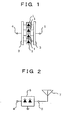
- Fig. 1 is a diagram showing a photodiode according to Embodiment 1 of the present invention.
- a plurality of photodiode elements 1 are arranged to form a photodiode array.
- a modulated light that has been input to a light input terminal 4 is branched by an optical branching filter circuit 2, and then input to the plurality of photodiode elements 1.
- Electric signals that have been detected by the photodiode elements 1 are combined together by an electric power combining circuit 3, and output from an electric output terminal 5.
- transmission paths of the light which is branched by the optical branching filter circuit 2 and input to the plurality of photodiode elements 1 are substantially identical in the length with each other as compared with the order of the wavelength of the modulated microwave over all of the paths.
- the electric signals that have been detected by the plurality of photodiode elements 1 are combined in electric power at the substantially same phase, and output from the electric output terminal 5. For that reason, the electric powers that are output from the respective photodiode elements 1 are efficiently combined together, thereby enabling a large electric power to be obtained.
- an RF current I PD of the current signals that are output from the photodiodes is represented by the following Expression 1.
- I PD ⁇ ⁇ I CW ⁇ m 2
- ⁇ is a quantum efficiency
- P cw is an input light power (a mean value of the modulated light power)
- m is a modulation degree.
- the RF electric power P PD that is obtained when the output current is connected to the output circuit having an impedance Z o is represented by the following Expression 2.
- the electric power of the RF electric output that is output from the photodiodes increases in proportion to the second power of the power of the light that is input to the photodiodes. This means that the electric output power can be remarkably increased as the light that is input to the photodiodes is increased.
- the photodiode array shown in Fig. 1 when the plurality of photodiode elements 1 are used, the respective photodiode elements 1 are prevented from being saturated even if the high-power light is input. For that reason, the large output RF electric power can be obtained. Also, the input light power is increased, thereby making it possible to obtain the output RF electric power larger than the input light power.
- the photodiode array shown in Fig. 1 has the advantage in that the large output power can be readily obtained without any necessity to match the delay time or match the output impedances of the respective elements as in the conventional traveling wave photodiode.
- the output electric signal power P PD is in proportion to the second power of a mean value P CW of the input modulated light power through Expression 2. Therefore, the output electric signal power P PD is always made larger than the mean value P CW of the input modulated light power when the mean value P CW of the input modulated light power is increased to be a specific value or more, from the above expression.
- Fig. 2 is a diagram showing an optical microwave transmission receiver according to Embodiment 2 of the present invention.
- a photodiode array 6 having the same configuration as that in Embodiment 1 shown in Fig. 1 is input with a light modulated signal from the light input terminal 4.
- the light modulated signal is detected by the photodiode array 6 and output from the electric output terminal 5 as the RF electric signal.
- the RF electric signal is input to an antenna 7 and radiated toward a space as the electromagnetic wave from the antenna 7.
- the electric signal that is output from the photodiode array 6 is connected directly to the antenna 7 without being input to the amplifier circuit such as an amplifier.
- the amplifier circuit required up to now is not required with the results that not only the device can be downsized, but also it is unnecessary to supply a required electric power to the amplifier circuit, to thereby reduce the power consumption.
- the electric power line that supplies the electric power to the amplifier circuit is not required, there is advantage in that there is no electromagnetic interference that occurs through the electric power line, and the low electromagnetic interference characteristic inherent to the optical fiber radio communication can be obtained.
- Fig. 2 shows a case in which the output of the photodiode array 6 is connected directly to the antenna 7.
- a passive circuit such as a filter or a branching filter can be inserted between the photodiode array 6 and the antenna 7.
- a branching such as a branching filter or a circulator can be disposed to add a circuit for a signal that is received from the antenna 7.
- this case can obtain the advantages of the present invention.
- Fig. 3 is a diagram showing a photodiode array according to Embodiment 3 of the present invention.
- the photodiode array 6 shown in Fig. 3 detects, as in Embodiments 1 and 2, a light modulation signal that is input from the light input terminal 4, and outputs the light modulation signal from the electric output terminal 5 as the RF electric signal.
- the photodiode array 6 shown in Fig. 3 is connected with an electric power supply photodiode 8 via a bias.
- the electric power supply photodiode 8 constitutes electric power converting means for converting the light that has been input to an electric power supply light input terminal 9 by the optical fiber into an electric energy to supply the converted electric energy to the photodiode array 6 as a bias power supply.
- the power of the photodiode itself can be supplied by light, and the photodiode that does not require at all an internal power supply or the electric power supply from the external is obtained. For that reason, there can be obtained a high-power photodiode that does not suffer at all from a problem with the size or weight of the power supply circuit or the electric power line, or a problem with the electromagnetic interference.
- Fig. 4 is a diagram showing a photodiode array according to Embodiment 4 of the present invention.
- the photodiode array 6 shown in Fig. 4 is the same configuration as that in Embodiment 1 shown in Fig. 1, and inputs a light modulation signal from the light input terminal 4.
- the light modulation signal is detected by the photodiode array 6, and output from the electric output terminal 5 as an RF electric signal.
- the electric energy that has been converted by the electric power supply photodiode 8 is supplied as the bias power supply and operates, as in Embodiment 3 shown in Fig. 3.
- the electric energy that is generated by the electric power supply photodiode 8 is temporarily accumulated in an accumulator 10 as accumulating means, and thereafter supplied to the photodiode array 6 as the bias power supply.
- the stable bias power supply can be supplied to the photodiode array 6, thereby making it possible to obtain the photodiode array that stably operates.
- the above embodiment shows a case in which the electric power supply photodiode 8 is used in order to obtain the electric power energy that is supplied to the photodiode array 6.
- the present invention is not limited to the above-mentioned configuration, and the electric power energy can be obtained by a solar cell instead of the photodiode.
- the photodiode array 6 that operates only with the aid of light can be obtained.
- the optical microwave transmission system receiver when the above-mentioned photodiode array 6 is applied to the optical microwave transmission system receiver, there is advantage in that the optical microwave transmission system receiver that is downsized, low in the power consumption, and extremely small in the electromagnetic interference can be obtained.
Landscapes
- Optical Communication System (AREA)
- Light Receiving Elements (AREA)
Abstract
Description
- The present invention relates to a photodiode array and an optical microwave transmission system receiver in which a plurality of photodiodes are connected in parallel to each other, thereby enabling a large electric power to be output.
- A photodiode has been widely employed as a photodetector that operates at high speed in an optical transmission device. Similarly, in an optical fiber radio communication device, the photodiode is essential as a key device. The optical fiber radio communication device is a transmission device having various advantages by which the transmission of a broad band and high capacity is enabled, various processor circuits can be downsized because the wavelength of light is short, a transmission loss is very low, and an electromagnetic interference is extremely reduced.
- In the optical fiber radio communication device, light is modulated according to an RF electric signal and transmitted, and the modulated light is detected by a photodiode, to thereby reproduce an original RF electric signal. The reproduced RF electric signal is transmitted to a succeeding processor circuit or radiated toward a space by means of an antenna.
- In general, an electric signal that is output from the photodiode is very weak. For that reason, when the electric signal that is extracted from the photodiode is transmitted to a circuit at a post-stage, it is necessary to amplify the signal with the aid of an amplifier circuit such as amplifier. For example, even in a case where the signal that has been transmitted through the optical fiber radio communication is radiated toward the space from the antenna, it is necessary to provide an electric power for radiating the electric signal toward the space after the electric signal has been detected by the photodiode, so the electric signal needs to be amplified by means of an amplifier circuit.
- However, a power supply is required in an amplifier circuit such as an amplifier involving a power consumption. In addition, a space for the amplifier circuit is required, so it is difficult to downsize the device. Further, an electric power line that supplies an electric power is required, and an electromagnetic interference occurs due to an electromagnetic field from the electric power line, thereby making it impossible to sufficiently utilize the features of the optical fiber radio communication device with no electromagnetic interference.
- As a method of increasing the electric power of an output electric signal from a photodiode, there has been proposed a traveling wave photodiode (for example, refer to Patent Document 1). This inputs a light to a plurality of photodiodes with a delay time bits by bits, and extracts output electric signals gradually with a delay time so as to cancel the delay time that has been given previously. However, in this method, since it is necessary to perfectly match those delay times with each other, and the impedance matching at the time of combining the electric powers is difficult, the output electric power that is actually obtained is not yet limited under the existing circumstances.
- Patent Document 1:
WO 2003-516641 - As described above, in the conventional photodiode of this type, the output electric signal is very weak, so an amplifier circuit is required at a post-stage. There are disadvantages such as the upsized device, the increased power consumption, or the deteriorated non-electromagnetic interference.
- The present invention has been made to solve the above-mentioned problems, and an object of the present invention is to provide a photodiode array that is capable of outputting an electric signal with a large electric power. Another object of the present invention is to provide an optical microwave transmission system receiver that supplies an electric power with the aid of an optical fiber and does not require the electric power line from the external.
- A photodiode array according to the present invention is characterized by branching an input modulation light, inputting the branched modulation lights to a plurality of photodiode elements, connecting electric output terminals of the plurality of photodiode elements in parallel to each other, and extracting a combined electric output.
- Further, an optical microwave transmission system receiver according to the present invention is characterized in that the electric output terminal of the photodiode array is connected to an antenna without an intermediation of an amplifier circuit.
- Still further, an photodiode array according to the present invention is characterized by further including: converting means for converting a light signal that is transmitted through an optical fiber into an electric energy to supply the photodiode array with the electric energy as a bias power supply.
- Yet further, an photodiode array according to the present invention is characterized by further including: accumulating means for accumulating the electric energy that has been converted by the converting means to supply the photodiode array with the accumulated electric energy as a bias power supply.
- In addition, the optical microwave transmission system receiver according to the present invention is characterized in that the photodiode array is used therein, and there is no electric power line from the external.
- According to the present invention, there can be obtained a photodiode array that is capable of outputting the electric signal with high power, and also there can be obtained an optical microwave transmission system receiver that supplies an electric power with the aid of the optical fiber and does not require the electric power line from the external at all.
-
- Fig. 1 is a diagram showing a photodiode array according to
Embodiment 1 of the present invention. - Fig. 2 is a diagram showing an optical microwave transmission system receiver according to
Embodiment 2 of the present invention. - Fig. 3 is a diagram showing a photodiode array according to
Embodiment 3 of the present invention. - Fig. 4 is a diagram showing a photodiode array according to
Embodiment 4 of the present invention. - Fig. 1 is a diagram showing a photodiode according to
Embodiment 1 of the present invention. As shown in Fig. 1, a plurality ofphotodiode elements 1 are arranged to form a photodiode array. A modulated light that has been input to alight input terminal 4 is branched by an opticalbranching filter circuit 2, and then input to the plurality ofphotodiode elements 1. Electric signals that have been detected by thephotodiode elements 1 are combined together by an electricpower combining circuit 3, and output from anelectric output terminal 5. - Referring to Fig. 1, transmission paths of the light which is branched by the optical
branching filter circuit 2 and input to the plurality ofphotodiode elements 1 are substantially identical in the length with each other as compared with the order of the wavelength of the modulated microwave over all of the paths. - Accordingly, the electric signals that have been detected by the plurality of
photodiode elements 1 are combined in electric power at the substantially same phase, and output from theelectric output terminal 5. For that reason, the electric powers that are output from therespective photodiode elements 1 are efficiently combined together, thereby enabling a large electric power to be obtained. - In general, when the photodiodes are not saturated, an RF current IPD of the current signals that are output from the photodiodes is represented by the
following Expression 1.
- In this expression, η is a quantum efficiency, Pcw is an input light power (a mean value of the modulated light power), and m is a modulation degree. The RF electric power PPD that is obtained when the output current is connected to the output circuit having an impedance Zo is represented by the following
Expression 2.
- Accordingly, the electric power of the RF electric output that is output from the photodiodes increases in proportion to the second power of the power of the light that is input to the photodiodes. This means that the electric output power can be remarkably increased as the light that is input to the photodiodes is increased.
- In the photodiode array shown in Fig. 1, when the plurality of
photodiode elements 1 are used, therespective photodiode elements 1 are prevented from being saturated even if the high-power light is input. For that reason, the large output RF electric power can be obtained. Also, the input light power is increased, thereby making it possible to obtain the output RF electric power larger than the input light power. In addition, the photodiode array shown in Fig. 1 has the advantage in that the large output power can be readily obtained without any necessity to match the delay time or match the output impedances of the respective elements as in the conventional traveling wave photodiode. - In other words, the output electric signal power PPD is in proportion to the second power of a mean value PCW of the input modulated light power through
Expression 2. Therefore, the output electric signal power PPD is always made larger than the mean value PCW of the input modulated light power when the mean value PCW of the input modulated light power is increased to be a specific value or more, from the above expression. - However, in the conventional photodiode, when the mean value PCW of the modulated light power is increased, the photo diodes are saturated, and
Expression 2 is not satisfied. For that reason, it is actually difficult to make the output electric signal power PPD larger than the power value PCW of the modulated light power. - In the photodiode array shown in Fig. 1, since a plurality of
photodiode elements 1 are connected in parallel,Expression 2 is satisfied as it is even if the mean value PCW of the modulated light power is made larger without saturating therespective photodiode elements 1. Accordingly, it is possible to make the output electric signal power PPD larger than the mean value PCW of the input modulated light power. - Fig. 2 is a diagram showing an optical microwave transmission receiver according to
Embodiment 2 of the present invention.
In the optical microwave transmission receiver shown in Fig. 2, aphotodiode array 6 having the same configuration as that inEmbodiment 1 shown in Fig. 1 is input with a light modulated signal from thelight input terminal 4. The light modulated signal is detected by thephotodiode array 6 and output from theelectric output terminal 5 as the RF electric signal. In addition, the RF electric signal is input to an antenna 7 and radiated toward a space as the electromagnetic wave from the antenna 7. - In the optical microwave transmission receiver shown in Fig. 2, the electric signal that is output from the
photodiode array 6 is connected directly to the antenna 7 without being input to the amplifier circuit such as an amplifier. The reason is that the electric signal can be radiated directly from the antenna 7 since the electric power of the electric signal that is output from thephotodiode array 6 is sufficiently large, unlike the conventional art. For that reason, the amplifier circuit required up to now is not required with the results that not only the device can be downsized, but also it is unnecessary to supply a required electric power to the amplifier circuit, to thereby reduce the power consumption. Also, since the electric power line that supplies the electric power to the amplifier circuit is not required, there is advantage in that there is no electromagnetic interference that occurs through the electric power line, and the low electromagnetic interference characteristic inherent to the optical fiber radio communication can be obtained. - Fig. 2 shows a case in which the output of the
photodiode array 6 is connected directly to the antenna 7. However, the present invention is not limited to this configuration, but a passive circuit such as a filter or a branching filter can be inserted between thephotodiode array 6 and the antenna 7. Also, a branching such as a branching filter or a circulator can be disposed to add a circuit for a signal that is received from the antenna 7. Similarly, this case can obtain the advantages of the present invention. - Fig. 3 is a diagram showing a photodiode array according to
Embodiment 3 of the present invention. Thephotodiode array 6 shown in Fig. 3 detects, as inEmbodiments light input terminal 4, and outputs the light modulation signal from theelectric output terminal 5 as the RF electric signal. In addition, thephotodiode array 6 shown in Fig. 3 is connected with an electricpower supply photodiode 8 via a bias. - The electric
power supply photodiode 8 constitutes electric power converting means for converting the light that has been input to an electric power supply light input terminal 9 by the optical fiber into an electric energy to supply the converted electric energy to thephotodiode array 6 as a bias power supply. - For that reason, the power of the photodiode itself can be supplied by light, and the photodiode that does not require at all an internal power supply or the electric power supply from the external is obtained. For that reason, there can be obtained a high-power photodiode that does not suffer at all from a problem with the size or weight of the power supply circuit or the electric power line, or a problem with the electromagnetic interference.
- Fig. 4 is a diagram showing a photodiode array according to
Embodiment 4 of the present invention. Thephotodiode array 6 shown in Fig. 4 is the same configuration as that inEmbodiment 1 shown in Fig. 1, and inputs a light modulation signal from thelight input terminal 4. The light modulation signal is detected by thephotodiode array 6, and output from theelectric output terminal 5 as an RF electric signal. - Also, the electric energy that has been converted by the electric
power supply photodiode 8 is supplied as the bias power supply and operates, as inEmbodiment 3 shown in Fig. 3. In this case, the electric energy that is generated by the electricpower supply photodiode 8 is temporarily accumulated in an accumulator 10 as accumulating means, and thereafter supplied to thephotodiode array 6 as the bias power supply. - For that reason, even if the magnitude of the electric power of the light that is input to the electric
power supply photodiode 8 varies, the stable bias power supply can be supplied to thephotodiode array 6, thereby making it possible to obtain the photodiode array that stably operates. - The above embodiment shows a case in which the electric
power supply photodiode 8 is used in order to obtain the electric power energy that is supplied to thephotodiode array 6. However, the present invention is not limited to the above-mentioned configuration, and the electric power energy can be obtained by a solar cell instead of the photodiode. Similarly, in this case, thephotodiode array 6 that operates only with the aid of light can be obtained. - Also, when the above-mentioned
photodiode array 6 is applied to the optical microwave transmission system receiver, there is advantage in that the optical microwave transmission system receiver that is downsized, low in the power consumption, and extremely small in the electromagnetic interference can be obtained.
Claims (5)
- A photodiode array characterized by branching an input modulation light, inputting the branched modulation lights to a plurality of photodiode elements, connecting electric output terminals of the plurality of photodiode elements in parallel to each other, and extracting a combined electric output.
- An optical microwave transmission system receiver characterized in that the electric output terminal of the photodiode array according to claim 1 is connected to an antenna without an intermediation of an amplifier circuit.
- A photodiode array according to claim 1 characterized by further comprising: converting means for converting a light signal that is transmitted through an optical fiber into an electric energy to supply the electric energy as a bias power supply.
- A photodiode array according to claim 3 characterized by further comprising: accumulating means for accumulating the electric energy that has been converted by the converting means to supply the accumulated electric energy as a bias power supply.
- An optical microwave transmission system receiver characterized by using the photodiode array according to claim 3 or 4.
Applications Claiming Priority (1)
| Application Number | Priority Date | Filing Date | Title |
|---|---|---|---|
| PCT/JP2005/008295 WO2006120723A1 (en) | 2005-05-02 | 2005-05-02 | Photodiode array and optical microwave transmission system receiver |
Publications (3)
| Publication Number | Publication Date |
|---|---|
| EP1879236A1 true EP1879236A1 (en) | 2008-01-16 |
| EP1879236A4 EP1879236A4 (en) | 2013-01-09 |
| EP1879236B1 EP1879236B1 (en) | 2016-09-28 |
Family
ID=37396247
Family Applications (1)
| Application Number | Title | Priority Date | Filing Date |
|---|---|---|---|
| EP05737217.9A Expired - Lifetime EP1879236B1 (en) | 2005-05-02 | 2005-05-02 | Photodiode array and optical microwave transmission system receiver |
Country Status (4)
| Country | Link |
|---|---|
| US (1) | US7723666B2 (en) |
| EP (1) | EP1879236B1 (en) |
| JP (1) | JP4675961B2 (en) |
| WO (1) | WO2006120723A1 (en) |
Families Citing this family (2)
| Publication number | Priority date | Publication date | Assignee | Title |
|---|---|---|---|---|
| US7547150B2 (en) * | 2007-03-09 | 2009-06-16 | Corning Cable Systems, Llc | Optically addressed RFID elements |
| JP7469705B2 (en) * | 2020-09-14 | 2024-04-17 | 日本電信電話株式会社 | Optical power receiving device, communication device, and optical power receiving method |
Family Cites Families (12)
| Publication number | Priority date | Publication date | Assignee | Title |
|---|---|---|---|---|
| US5029306A (en) * | 1989-08-10 | 1991-07-02 | The Boeing Company | Optically fed module for phased-array antennas |
| US5001336A (en) * | 1989-12-11 | 1991-03-19 | The Boeing Company | Optical signal summing device |
| JPH08331061A (en) | 1995-05-31 | 1996-12-13 | Fuji Electric Co Ltd | Optical signal transmission device |
| JPH11154762A (en) * | 1997-11-20 | 1999-06-08 | Tokin Corp | Photovoltaic device |
| JP3465630B2 (en) | 1999-06-02 | 2003-11-10 | 株式会社村田製作所 | Antenna duplexer and communication device |
| JP2001068717A (en) | 1999-08-25 | 2001-03-16 | Nippon Telegr & Teleph Corp <Ntt> | Traveling-wave semiconductor photodetector |
| US6418248B1 (en) | 1999-12-07 | 2002-07-09 | Hrl Laboratories, Llc | Traveling-wave photodetector |
| JP2001189488A (en) | 1999-12-27 | 2001-07-10 | Toshiba Corp | Integrated optical semiconductor device |
| JP2004328903A (en) * | 2003-04-24 | 2004-11-18 | Seiko Instruments Inc | Optically-driven micro-actuator |
| DE102004003993A1 (en) * | 2003-08-12 | 2005-03-17 | Leica Microsystems Heidelberg Gmbh | Device for detecting photons of a light beam |
| US8204381B2 (en) * | 2003-12-30 | 2012-06-19 | Intel Corporation | Broadband radio transceiver with optical transform |
| JP4221716B2 (en) * | 2004-03-04 | 2009-02-12 | 横河電機株式会社 | Optical logic element |
-
2005
- 2005-05-02 EP EP05737217.9A patent/EP1879236B1/en not_active Expired - Lifetime
- 2005-05-02 WO PCT/JP2005/008295 patent/WO2006120723A1/en not_active Ceased
- 2005-05-02 US US11/884,205 patent/US7723666B2/en not_active Expired - Fee Related
- 2005-05-02 JP JP2007526716A patent/JP4675961B2/en not_active Expired - Fee Related
Also Published As
| Publication number | Publication date |
|---|---|
| WO2006120723A1 (en) | 2006-11-16 |
| US20090121118A1 (en) | 2009-05-14 |
| JPWO2006120723A1 (en) | 2008-12-18 |
| JP4675961B2 (en) | 2011-04-27 |
| EP1879236A4 (en) | 2013-01-09 |
| US7723666B2 (en) | 2010-05-25 |
| EP1879236B1 (en) | 2016-09-28 |
Similar Documents
| Publication | Publication Date | Title |
|---|---|---|
| TW586277B (en) | Remotely locatable RF power amplification system | |
| CN112532325B (en) | Multi-dimensional multiplexing photon terahertz communication system | |
| KR102503881B1 (en) | Terahertz signal transmission apparatus and terahertz signal transmission method using the same | |
| CN106230516B (en) | Radar communication based on microwave photon fights integral system | |
| CN103117803A (en) | Space-borne microwave and laser communication link integrating system and application method | |
| US20260009672A1 (en) | Distributed acoustic sensing system based on optical neural network and all-optical integration method | |
| Souza et al. | Performance of an optically powered radio-over-fiber system exploiting raman amplification | |
| CN115079139B (en) | Photon time-stretching coherent radar chip | |
| EP1879236A1 (en) | Photodiode array and optical microwave transmission system receiver | |
| CN105846899A (en) | Broadband radio frequency signal optical fiber transmission system | |
| CN113608227B (en) | Photon-assisted radar frequency mixing and direct wave self-interference cancellation integrated device and method | |
| KR101325247B1 (en) | Method and apparatus for generating terahertz continuous wave | |
| CN113391268A (en) | Microwave photon frequency measurement realization method and system | |
| CN100568783C (en) | Bidirectional transmission device and signal transmission method of millimeter wave optical fiber transmission system based on insertion pilot method | |
| Singh et al. | Electronic-photonic millimeter-wave sensing element based on monolithically integrated LNA and triple-cavity ring modulator | |
| Niehenke et al. | An optical link for W-band transmit/receive applications | |
| Esman et al. | Photonics for microwave generation, transmission, and processing | |
| CN116094602B (en) | A spaceborne laser communication terminal and its signal processing method | |
| CN119209171B (en) | Integrated photoelectric oscillator | |
| Wakatsuki et al. | High-speed photodiode and optical receiver technologies | |
| Smith et al. | A broadband integrated photonic-antenna interface for multiservice millimeter-wave fiber-wireless applications | |
| JP3093338B2 (en) | Fiber optic link | |
| Umezawa et al. | Dual Band Millimeter-Wave Integrated Photoreceiver | |
| Singh et al. | RF-CMOS Electronic-Photonic Sensing Elements for Millimeter-wave Front-end Systems-on-Chip: Enabling mm-wave Array Scaling/Disaggregation for Radar and Extreme Massive MIMO | |
| Konkol et al. | High-Power Photonic Phased Array Antennas |
Legal Events
| Date | Code | Title | Description |
|---|---|---|---|
| PUAI | Public reference made under article 153(3) epc to a published international application that has entered the european phase |
Free format text: ORIGINAL CODE: 0009012 |
|
| 17P | Request for examination filed |
Effective date: 20070717 |
|
| AK | Designated contracting states |
Kind code of ref document: A1 Designated state(s): FR GB |
|
| DAX | Request for extension of the european patent (deleted) | ||
| RBV | Designated contracting states (corrected) |
Designated state(s): FR GB |
|
| A4 | Supplementary search report drawn up and despatched |
Effective date: 20121211 |
|
| RIC1 | Information provided on ipc code assigned before grant |
Ipc: H01L 31/10 20060101AFI20121205BHEP |
|
| 17Q | First examination report despatched |
Effective date: 20130408 |
|
| GRAP | Despatch of communication of intention to grant a patent |
Free format text: ORIGINAL CODE: EPIDOSNIGR1 |
|
| RIC1 | Information provided on ipc code assigned before grant |
Ipc: H04B 10/80 20130101AFI20160405BHEP Ipc: H01L 31/101 20060101ALI20160405BHEP |
|
| INTG | Intention to grant announced |
Effective date: 20160506 |
|
| RIN1 | Information on inventor provided before grant (corrected) |
Inventor name: NAGATSUKA, TSUTOMU C/O MITSUBISHI DENKI K.K. Inventor name: ISHIMURA, EITARO C/O MITSUBISHI DENKI K.K. Inventor name: HIRANO, YOSHIHITO C/O MITSUBISHI DENKI K.K. Inventor name: ISHII, RYUJI C/O MITSUBISHI DENKI K.K. Inventor name: AOYAGI, TOSHITAKA C/O MITSUBISHI DENKI K.K. Inventor name: SATO, MASAHITO C/O MITSUBISHI DENKI K.K. Inventor name: AKIYAMA, TOMOHIRO C/O MITSUBISHI DENKI K.K. |
|
| GRAS | Grant fee paid |
Free format text: ORIGINAL CODE: EPIDOSNIGR3 |
|
| GRAA | (expected) grant |
Free format text: ORIGINAL CODE: 0009210 |
|
| AK | Designated contracting states |
Kind code of ref document: B1 Designated state(s): FR GB |
|
| REG | Reference to a national code |
Ref country code: GB Ref legal event code: FG4D |
|
| REG | Reference to a national code |
Ref country code: FR Ref legal event code: PLFP Year of fee payment: 13 |
|
| PLBE | No opposition filed within time limit |
Free format text: ORIGINAL CODE: 0009261 |
|
| STAA | Information on the status of an ep patent application or granted ep patent |
Free format text: STATUS: NO OPPOSITION FILED WITHIN TIME LIMIT |
|
| 26N | No opposition filed |
Effective date: 20170629 |
|
| REG | Reference to a national code |
Ref country code: FR Ref legal event code: PLFP Year of fee payment: 14 |
|
| PGFP | Annual fee paid to national office [announced via postgrant information from national office to epo] |
Ref country code: GB Payment date: 20180329 Year of fee payment: 14 |
|
| REG | Reference to a national code |
Ref country code: GB Ref legal event code: 746 Effective date: 20190117 |
|
| PGFP | Annual fee paid to national office [announced via postgrant information from national office to epo] |
Ref country code: FR Payment date: 20190410 Year of fee payment: 15 |
|
| GBPC | Gb: european patent ceased through non-payment of renewal fee |
Effective date: 20190502 |
|
| PG25 | Lapsed in a contracting state [announced via postgrant information from national office to epo] |
Ref country code: GB Free format text: LAPSE BECAUSE OF NON-PAYMENT OF DUE FEES Effective date: 20190502 |
|
| PG25 | Lapsed in a contracting state [announced via postgrant information from national office to epo] |
Ref country code: FR Free format text: LAPSE BECAUSE OF NON-PAYMENT OF DUE FEES Effective date: 20200531 |