EP1876600A1 - Control integrated circuit of a charge pump - Google Patents
Control integrated circuit of a charge pump Download PDFInfo
- Publication number
- EP1876600A1 EP1876600A1 EP06425465A EP06425465A EP1876600A1 EP 1876600 A1 EP1876600 A1 EP 1876600A1 EP 06425465 A EP06425465 A EP 06425465A EP 06425465 A EP06425465 A EP 06425465A EP 1876600 A1 EP1876600 A1 EP 1876600A1
- Authority
- EP
- European Patent Office
- Prior art keywords
- value
- charge pump
- voltage
- integrated circuit
- vout
- Prior art date
- Legal status (The legal status is an assumption and is not a legal conclusion. Google has not performed a legal analysis and makes no representation as to the accuracy of the status listed.)
- Granted
Links
Images



Classifications
-
- G—PHYSICS
- G11—INFORMATION STORAGE
- G11C—STATIC STORES
- G11C5/00—Details of stores covered by group G11C11/00
- G11C5/14—Power supply arrangements, e.g. power down, chip selection or deselection, layout of wirings or power grids, or multiple supply levels
- G11C5/145—Applications of charge pumps; Boosted voltage circuits; Clamp circuits therefor
-
- G—PHYSICS
- G11—INFORMATION STORAGE
- G11C—STATIC STORES
- G11C16/00—Erasable programmable read-only memories
- G11C16/02—Erasable programmable read-only memories electrically programmable
- G11C16/06—Auxiliary circuits, e.g. for writing into memory
- G11C16/10—Programming or data input circuits
- G11C16/12—Programming voltage switching circuits
Definitions
- the present invention relates to an integrated control circuit for a charge pump.
- a typical initial wiring diagram is shown in figure 1; a charge pump 1 generates an output voltage Vout that is sent to a comparator 2.
- the latter compares the voltage Vout with a voltage Vreg, i.e. the desired regulating voltage that is generated from a known and extremely stable reference voltage, for example a BandGap circuit. If Vout>Vreg the comparator 2 sends a logic signal Von to a control circuit 3, having a clock input pulse CLOCK, that blocks transmission of the CLOCK pulses to a phase generator 4 suitable for supplying the charge pump 1.
- the charge pump 1 starts to discharge until the voltage Vout becomes less than the voltage Vreg.
- the charge pump 1 if it is a vacuum pump, is switched off in order not to dissipate power unnecessarily; in the presence of a charge that requires current, the circuit lets the clock pulses pass so as to compensate for the decrease in output voltage Vout due to the delivered charge.
- the circuit comprises a resistive divider formed by the series of two resistances Rup and Rdown arranged between Vout and ground GND.
- the voltage Vr at the heads of the resistance Rdown is sampled and compared with a reference voltage Vbg supplied by a bandgap circuit by means of a comparator 5.
- the signal at the comparator output is the signal Von that allows or does not allow the passage of the clock pulses CLOCK from the circuit 3 to the phase generator 4.
- two capacitors Cup and Cdown are shown arranged at the heads of the respective resistances Rup and Rdown and necessary for compensating parasitic capacity.
- the regulating voltage obtained as an average value arises from Vout Vbg*(1+Rup/Rdown).
- the circuit disclosed in figures 1 and 2 is used both for the charge pump used in the reading operations of the EEPROM memories and for the charge pump used in the writing operations thereof.
- the output voltage of the charge pump is carried on the memory cells in ramp mode so as not to risk the breakage of the oxide layers of the memory cells.
- the ramp generator charges a capacitor with a direct current to obtain a linear increase.
- FIG 3 there is shown a typical diagram of the regulation of the charge pump with a ramp generating circuit used for the EEPROM cells.
- the ramp generating circuit comprises an operational amplifier 6 having the input voltage Vbg on the inverting terminal and the voltage Vbot on the non-inverting terminal; the output of the operational amplifier 6 controls a transistor PMOS M1 having the source terminal connected to the output voltage Vout from the charge pump 3 of the circuit in figure 1.
- the drain terminal LS of the transistor M1 is connected to a capacitor C1 having the other terminal connected to the voltage Vbot at the heads of a current generator Ic connected to ground GND.
- the node LS is charged at a constant tilt equal to Ic/C1; by modulating the current the ascent speed of the voltage is varied appropriately.
- the node LS controls a first plurality of transistors identical to the plurality of transistors suitable for selecting the memory cells; each selection transistor has the voltage LS on the gate terminal whilst the voltage on the source terminal of each transistor of the first plurality is the same as the ramp voltage Vramp decreased of the threshold voltage of the transistor. In this way, coupling of the voltage Vramp and the voltage actually present on the memory cells are assured.
- the regulating node controlled directly is the node VP0 and the output voltage Vout of the charge pump is controlled indirectly through the transistors 125 that, through the coupling with those of the latch part of the memory cells and with the selection transistors of the memory cells, replicate exactly the programming and deletion path.
- a voltage drop may be generated on the selection transistors that distances the voltage level Vramp from the expected value.
- the copy of the latch and selection transistors are a waste of space.
- the object of the present invention is to provide an integrated control circuit for a charge pump that overcomes the aforementioned drawbacks.
- an integrated control circuit for a charge pump comprising a first device suitable for regulating the output voltage of the charge pump, characterised in that it comprises a second device suitable for increasing the output voltage from the charge pump with a set ramp and means suitable for activating said first device and providing it with a first value of a supply signal in a first period of time and suitable for activating said second device and for providing it with a second value of the supply signal that is greater than the first value in a second period of time after the first in such a way that the output voltage of the charge pump ascends a ramp from a first value to a second value greater than the first value, said second value being fixed by the reactivation of the first device.
- the circuit in figure 4 is suitable for regulating the output voltage Vout from a charge pump.
- the dimension of the NMOS transistor N2 is N times greater than the dimension of the transistor N1 so as to produce a current Ireg at a value selected on the basis of the value of the voltage Vout.
- the circuit branch comprising the transistor N2 also comprises a resistance R connected to the source terminal of the transistor N2 and to the voltage Vout.
- the output voltage of the charge pump Vout depends exclusively on the bandgap voltage Vbg, which is a voltage that is stable with respect to temperature and voltage variations; each variation of a physical or technological nature to the value of the resistances is insignificant as the resistances appear in the form of a ratio.
- the transistors P1 and P2 are part of a block 112.
- Another transistor block 113 comprising a PMOS mirror, enables a current Iramp to be taken to a current mirror M10-M11 that enables the current Iramp to be mirrored on a circuit branch comprising a capacitor C11 connected to the voltage Vout and to the drain terminal of the transistor M11.
- the voltage Vramp on the drain terminal of the transistor M11 is an input to the non-inverting terminal of an operational amplifier 11 having the voltage Vbg on the inverting terminal.
- the capacitor C11 is charged with a direct current Iramp provided by the mirror M10-M11. The voltage increases on a ramp given by Iramp/C.
- FIG 6 there is shown the circuit according to the invention that comprises the circuits of figures 4 and 5 where the outputs Reg12 and Reg1 of the respective amplifiers 11 and 12 are inputs to an OR gate 13 having the output signal Reg13; said signal is an inlet signal to the charge pump 1 that provides the output voltage Vout.
- the circuit according to the invention preferably comprises a logic circuitry 111 that acts on the blocks 112 and 113 formed respectively by PMOS transistors, that are suitable for carrying the current to the mirrors M10-M11 and N1-N2, to activate them and change the current to be taken to the ramp generator in figure 5 and to the regulator in figure 4.
- the operation of the circuit is as follows and is visible in figure 9.
- phase B the circuitry 111 activates the ramp generator by means of a precharge phase in which the node Vramp is taken to the value Vbg.
- the charge pump used in the case of EEPROM memories is of the reconfigurable type, i.e. it is made to operate with identical modules arranged parallel with low voltage levels, for example for reading the memory cells, or arranged in series when on the other hand a high voltage level is required, i.e. in the case of programming or deletion.
- a high voltage level is required, i.e. in the case of programming or deletion.
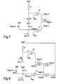
- the circuit arrangement comprises a PMOS transistor M15 having the source terminal connected to a supply voltage Vdd and the drain terminal connected to the voltage Vramp; by switching on the capacitive branch during the discharge of the capacitor C11 the latter is forced to evolve into a ramp.
- the ramp generator modulates through the output of the comparator 11 the descent of the voltage Vout.
- the transistor M15 has to have dimensions such as to ensure a certain tilt of the descent ramp in conditions of maximum charge. In this way, constant discharge time is ensured as the charge varies.
- the circuit in figure 8 differs from the circuit in figure 7 through the addition of a filter 20-21.
- the filter comprises a first AND gate 20 having the input signals Reg12 and the negated signal Vdisch, where Vdisch is the discharge voltage of the transistor M15.
- the output signal from the AND gate 20 is the input signal to the OR gate.
- An AND gate 21 has the input signals Reg11 and Vdisch and the output pilots a transistor M16 the drain terminal of which is connected to the voltage Vout whilst the source terminal is connected to ground. Said filter is necessary so that the signal Reg11 does not interfere with the information provided by the capacitive branch.
Landscapes
- Engineering & Computer Science (AREA)
- Power Engineering (AREA)
- Dc-Dc Converters (AREA)
- Read Only Memory (AREA)
Abstract
Description
- The present invention relates to an integrated control circuit for a charge pump.
- In EEPROM memories it is necessary that the high voltage levels of the order of 12 or 15 V that are generated by the charge pump for the programming and deletion operations are maintained at a virtually constant value whatever current delivery is required (the so-called driving capability), which is normally of the order of dozens of microamperes. This enables a stable and known output voltage to be available that cannot moreover exceed the limits set by the dielectric strength of the oxides, i.e. of the oxides of the transistors and of the capacitors, with the risk of damaging them permanently, i.e. producing perforations.
- A typical initial wiring diagram is shown in figure 1; a
charge pump 1 generates an output voltage Vout that is sent to acomparator 2. The latter compares the voltage Vout with a voltage Vreg, i.e. the desired regulating voltage that is generated from a known and extremely stable reference voltage, for example a BandGap circuit. If Vout>Vreg thecomparator 2 sends a logic signal Von to acontrol circuit 3, having a clock input pulse CLOCK, that blocks transmission of the CLOCK pulses to aphase generator 4 suitable for supplying thecharge pump 1. Thus thecharge pump 1 starts to discharge until the voltage Vout becomes less than the voltage Vreg. By means of said feedback a dynamic equilibrium is reached that determines the steady state Vout=Vreg. Once the regulating condition has been reached, thecharge pump 1, if it is a vacuum pump, is switched off in order not to dissipate power unnecessarily; in the presence of a charge that requires current, the circuit lets the clock pulses pass so as to compensate for the decrease in output voltage Vout due to the delivered charge. - In order to obtain the signal Von, a circuit is used that is shown in figure 2. The circuit comprises a resistive divider formed by the series of two resistances Rup and Rdown arranged between Vout and ground GND. The voltage Vr at the heads of the resistance Rdown is sampled and compared with a reference voltage Vbg supplied by a bandgap circuit by means of a
comparator 5. The signal at the comparator output is the signal Von that allows or does not allow the passage of the clock pulses CLOCK from thecircuit 3 to thephase generator 4. In figure 2 two capacitors Cup and Cdown are shown arranged at the heads of the respective resistances Rup and Rdown and necessary for compensating parasitic capacity. - The regulating voltage obtained as an average value arises from Vout=Vbg*(1+Rup/Rdown). The circuit disclosed in figures 1 and 2 is used both for the charge pump used in the reading operations of the EEPROM memories and for the charge pump used in the writing operations thereof.
- The output voltage of the charge pump is carried on the memory cells in ramp mode so as not to risk the breakage of the oxide layers of the memory cells. Normally the ramp generator charges a capacitor with a direct current to obtain a linear increase. In figure 3 there is shown a typical diagram of the regulation of the charge pump with a ramp generating circuit used for the EEPROM cells. The ramp generating circuit comprises an
operational amplifier 6 having the input voltage Vbg on the inverting terminal and the voltage Vbot on the non-inverting terminal; the output of theoperational amplifier 6 controls a transistor PMOS M1 having the source terminal connected to the output voltage Vout from thecharge pump 3 of the circuit in figure 1. The drain terminal LS of the transistor M1 is connected to a capacitor C1 having the other terminal connected to the voltage Vbot at the heads of a current generator Ic connected to ground GND. The node LS is charged at a constant tilt equal to Ic/C1; by modulating the current the ascent speed of the voltage is varied appropriately. - The node LS controls a first plurality of transistors identical to the plurality of transistors suitable for selecting the memory cells; each selection transistor has the voltage LS on the gate terminal whilst the voltage on the source terminal of each transistor of the first plurality is the same as the ramp voltage Vramp decreased of the threshold voltage of the transistor. In this way, coupling of the voltage Vramp and the voltage actually present on the memory cells are assured. In the diagram in figure 3 it is shown that the regulating node controlled directly is the node VP0 and the output voltage Vout of the charge pump is controlled indirectly through the
transistors 125 that, through the coupling with those of the latch part of the memory cells and with the selection transistors of the memory cells, replicate exactly the programming and deletion path. As said transistors that are a copy of the latch part and of the selection transistors are in the ramp generator, by regulating the node VP0 also the voltage Vramp is regulated, as VP0 is the maximum value of Vramp except for decoupling between the paths of the voltages in play. - Nevertheless, during, for example, the phase of programming the memory cells, a voltage drop may be generated on the selection transistors that distances the voltage level Vramp from the expected value.
- Furthermore, the copy of the latch and selection transistors are a waste of space.
- In view of the disclosed prior art, the object of the present invention is to provide an integrated control circuit for a charge pump that overcomes the aforementioned drawbacks.
- According to the present invention, this object is achieved by means of an integrated control circuit for a charge pump, said integrated circuit comprising a first device suitable for regulating the output voltage of the charge pump, characterised in that it comprises a second device suitable for increasing the output voltage from the charge pump with a set ramp and means suitable for activating said first device and providing it with a first value of a supply signal in a first period of time and suitable for activating said second device and for providing it with a second value of the supply signal that is greater than the first value in a second period of time after the first in such a way that the output voltage of the charge pump ascends a ramp from a first value to a second value greater than the first value, said second value being fixed by the reactivation of the first device.
- The features and advantages of the present invention will be clear from the following detailed description of a practical embodiment illustrated by way of non-limitative example in the attached drawings, in which:
- figure 1 is a diagram of a regulating system according to the prior art;
- figure 2 shows a circuit for obtaining a signal present in the circuit in figure 1;
- figure 3 there is shown a typical initial diagram of the ramp generating circuit used for the EEPROM cells;
- figure 4 shows a part of the integrated control circuit of a charge pump according to an embodiment of the present invention;
- figure 5 shows another part of the integrated control circuit of a charge pump according to an embodiment of the present invention;
- figure 6 shows the integrated control circuit of a charge pump according to an embodiment of the present invention;
- figure 7 shows an integrated control circuit of a charge pump according to a variation of the embodiment of the present invention;
- figure 8 shows an integrated control circuit of a charge pump according to another version of the embodiment of the present invention;
- figure 9 shows an operating simulation of the control circuit in figure 6.
- With reference to figure 4 there is shown a part of the integrated control circuit for a charge pump according to the present invention. The circuit in figure 4 is suitable for regulating the output voltage Vout from a charge pump. The circuit in figure 4 comprises a
first circuit block 10 comprising anoperational amplifier 11 at the inverting terminal of which there is present the voltage Vbg and at the non-inverting terminal of which there is present the voltage Vbgref at the heads of a resistance Rvbg arranged between the ground GND and the drain terminal of a PMOS transistor P1 having the source terminal connected to a reference voltage Vdd and the gate terminal connected to the output voltage Vpref from theoperational amplifier 11; in this way there is obtained a current Ivbgref=Vbg/Rvbg that by means of another PMOS transistor P2, which is mirror-connected to the transistor P1, is taken to another transistor N1 forming part of a mirror N1, N2. The dimension of the NMOS transistor N2 is N times greater than the dimension of the transistor N1 so as to produce a current Ireg at a value selected on the basis of the value of the voltage Vout. The circuit branch comprising the transistor N2 also comprises a resistance R connected to the source terminal of the transistor N2 and to the voltage Vout. Anoperational amplifier 12 makes the voltage VR=Vbg; as Vout=Vbg+R*Ireg and Ireg=N*Ivbg=N*Vbg/Rvbg, there is obtained Vout=Vbg*(1+RN/Rvbg), i.e. the output voltage of the charge pump Vout depends exclusively on the bandgap voltage Vbg, which is a voltage that is stable with respect to temperature and voltage variations; each variation of a physical or technological nature to the value of the resistances is insignificant as the resistances appear in the form of a ratio. The transistors P1 and P2 are part of ablock 112. - In order to obtain a voltage ramp it is necessary to use another circuit, as shown in figure 5. Another
transistor block 113, comprising a PMOS mirror, enables a current Iramp to be taken to a current mirror M10-M11 that enables the current Iramp to be mirrored on a circuit branch comprising a capacitor C11 connected to the voltage Vout and to the drain terminal of the transistor M11. The voltage Vramp on the drain terminal of the transistor M11 is an input to the non-inverting terminal of anoperational amplifier 11 having the voltage Vbg on the inverting terminal. The capacitor C11 is charged with a direct current Iramp provided by the mirror M10-M11. The voltage increases on a ramp given by Iramp/C. - In figure 6 there is shown the circuit according to the invention that comprises the circuits of figures 4 and 5 where the outputs Reg12 and Reg1 of the
respective amplifiers OR gate 13 having the output signal Reg13; said signal is an inlet signal to thecharge pump 1 that provides the output voltage Vout. The circuit according to the invention preferably comprises alogic circuitry 111 that acts on theblocks - In the initial phase A when the charge pump is at the lower regulating level Vlow polarized by means of an appropriate of value Ireg set by the
circuitry 111, the current Iramp is nil; in this condition VR=Vbg, Reg13=Reg12, Vramp=0 and Reg11=0. - Subsequently, in phase B, the
circuitry 111 activates the ramp generator by means of a precharge phase in which the node Vramp is taken to the value Vbg. - Subsequently, in the phase C, the
circuitry 111 takes the current Ireg to a value that is compatible with the upper regulating value Vhigh, and in this case the capacitor branch is active and after a transition Vramp=Vbg is obtained whilst Vr<<Vbg as the regulating voltage is below the final value. In this phase, Reg11=Reg13 and Reg12=0. - Subsequently, in the phase D, when the voltage Vr becomes the same as the voltage Vbg, the voltage Vramp is discharged to ground and Reg12=Reg13 is obtained. The capacitive branch switches off and only the non-capacitive branch controls the charge pump.
- The charge pump used in the case of EEPROM memories is of the reconfigurable type, i.e. it is made to operate with identical modules arranged parallel with low voltage levels, for example for reading the memory cells, or arranged in series when on the other hand a high voltage level is required, i.e. in the case of programming or deletion. In order for the reconfiguration after the formation of a voltage ramp and the subsequent discharge to be effective, i.e. so that the pump starts operating again with the modules arranged parallel rapidly without load dispersal, it is necessary for the pump to remain active during the discharge.
- This involves having to dimension with attention the discharge current, which has to be greater than driving capability, but not excessively so as not to have a discharge that is so fast as not to allow redistribution of the charges.
- In figures 7 and 8 there are circuit alternatives comprising the circuit in figure 6 with two different circuit arrangements for discharging capacity.
- In figure 7 the circuit arrangement comprises a PMOS transistor M15 having the source terminal connected to a supply voltage Vdd and the drain terminal connected to the voltage Vramp; by switching on the capacitive branch during the discharge of the capacitor C11 the latter is forced to evolve into a ramp. In fact if the PMOS transistor M15 is controlled by the signal Reg11, the ramp generator modulates through the output of the
comparator 11 the descent of the voltage Vout. The transistor M15 has to have dimensions such as to ensure a certain tilt of the descent ramp in conditions of maximum charge. In this way, constant discharge time is ensured as the charge varies. - The circuit in figure 8 differs from the circuit in figure 7 through the addition of a filter 20-21. The filter comprises a first AND
gate 20 having the input signals Reg12 and the negated signal Vdisch, where Vdisch is the discharge voltage of the transistor M15. The output signal from the ANDgate 20 is the input signal to the OR gate. An ANDgate 21 has the input signals Reg11 and Vdisch and the output pilots a transistor M16 the drain terminal of which is connected to the voltage Vout whilst the source terminal is connected to ground. Said filter is necessary so that the signal Reg11 does not interfere with the information provided by the capacitive branch.
Claims (10)
- Integrated control circuit for a charge pump (1), said integrated circuit comprising a first device suitable for regulating the output voltage (Vout) of the charge pump (1), characterised in that it comprises a second device suitable for increasing the output voltage (Vout) from the charge pump with a set ramp and means (111) suitable for activating said first device and providing it with a first value of a supply signal (Ireg) in a first period of time (A) and suitable for activating said second device and for providing it with a second value (Iramp) of the supply signal that is greater than the first value in a second period of time (C) after the first in such a way that the output voltage of the charge pump ascends a ramp from a first value (Vlow) to a second value (Vhigh) that is greater than the first value, said second value being fixed by the reactivation of the first device.
- Integrated circuit according to claim 1, characterised in that said supply signal is a current
- Integrated circuit according to claim 2, characterised in that said first device comprises a resistance (R) coupled with the output voltage (Vout) of the charge pump (1) and with the terminal of a comparator (12) having at the other terminal a reference voltage (Vbg), said resistance being traversed by the supply signal (Ireg).
- Integrated circuit according to claim 3, characterised in that said second device comprises a capacity (C11) coupled with the output voltage (Vout) of the charge pump (1) and with the terminal of a comparator (11) having at the other terminal said reference voltage (Vbg), said capacity (C11) being charged by the supply signal (Iramp).
- Integrated circuit according to claim 4, characterised in that said first period of time (A, B) comprises a first subperiod (A) wherein the voltage at the heads of the comparator (12) of the first device is made the same and a second subperiod (B) wherein the voltage at the heads of the comparator (11) of the second device is made the same.
- Integrated circuit according to claim 5, characterised in that it comprises an OR gate (13) having as inputs (Reg11, Reg12) the outputs of the comparators (11, 12) of the first and of the second device and the output (Reg13) of said OR gate being the input to the charge pump (1).
- Integrated circuit according to claim 5, characterised in that it comprises a ramp discharge circuit for the capacity (C11) of the second device.
- Integrated circuit according to claim 7, characterised in that said ramp discharge circuit comprises a transistor (M15) coupled with the capacity (C11), connected to the further supply signal (Vdd) and driven by the output signal (Reg11) from the comparator of the second device.
- Integrated circuit according to claim 8, characterised in that it comprises means (20, 21, M16) suitable for filtering the output signal from the comparator of the first device to prevent it interfering with the output signal from the comparator of the second device.
- Controlling method of the output voltage (Vout) from a charge pump (1) comprising setting a first value (Vlow) at said output voltage (Vout) and the ramp ascent with a preset ramp from said first value (Vlow) to a second value (Vhigh) greater than the first value.
Priority Applications (3)
| Application Number | Priority Date | Filing Date | Title |
|---|---|---|---|
| DE602006009091T DE602006009091D1 (en) | 2006-07-06 | 2006-07-06 | Integrated control circuit of a charge pump |
| EP06425465A EP1876600B1 (en) | 2006-07-06 | 2006-07-06 | Control integrated circuit of a charge pump |
| US11/771,157 US7602230B2 (en) | 2006-07-06 | 2007-06-29 | Control integrated circuit for a charge pump |
Applications Claiming Priority (1)
| Application Number | Priority Date | Filing Date | Title |
|---|---|---|---|
| EP06425465A EP1876600B1 (en) | 2006-07-06 | 2006-07-06 | Control integrated circuit of a charge pump |
Publications (2)
| Publication Number | Publication Date |
|---|---|
| EP1876600A1 true EP1876600A1 (en) | 2008-01-09 |
| EP1876600B1 EP1876600B1 (en) | 2009-09-09 |
Family
ID=37650653
Family Applications (1)
| Application Number | Title | Priority Date | Filing Date |
|---|---|---|---|
| EP06425465A Active EP1876600B1 (en) | 2006-07-06 | 2006-07-06 | Control integrated circuit of a charge pump |
Country Status (3)
| Country | Link |
|---|---|
| US (1) | US7602230B2 (en) |
| EP (1) | EP1876600B1 (en) |
| DE (1) | DE602006009091D1 (en) |
Families Citing this family (8)
| Publication number | Priority date | Publication date | Assignee | Title |
|---|---|---|---|---|
| US7872518B2 (en) * | 2008-07-31 | 2011-01-18 | Infineon Technologies Ag | Circuit and method for detecting, whether a voltage difference between two voltages is below a desired voltage difference, and protection circuit |
| US8336927B2 (en) | 2008-08-15 | 2012-12-25 | Luke Liang | Tilt latch with cantilevered angular extension |
| US8220846B2 (en) | 2008-08-15 | 2012-07-17 | Vision Industries Group, Inc. | Latch for tiltable sash windows |
| US8120411B1 (en) * | 2009-07-31 | 2012-02-21 | Altera Corporation | Charge pump with ramp rate control |
| EP2299576B1 (en) * | 2009-09-18 | 2014-06-18 | STMicroelectronics Srl | Low consumption voltage regulator for a high voltage charge pump, voltage regulation method, and memory device provided with said voltage regulator |
| US9088280B2 (en) | 2013-10-30 | 2015-07-21 | Freescale Semiconductor, Inc. | Body bias control circuit |
| US9929643B2 (en) | 2016-03-31 | 2018-03-27 | Nxp B.V. | Charge pump circuit and method for operating a charge pump circuit |
| CN108305659B (en) * | 2018-02-27 | 2020-08-25 | 上海贝岭股份有限公司 | Slope control circuit of erasing voltage of nonvolatile memory and nonvolatile memory |
Citations (3)
| Publication number | Priority date | Publication date | Assignee | Title |
|---|---|---|---|---|
| US6320796B1 (en) * | 2000-11-10 | 2001-11-20 | Marvell International, Ltd. | Variable slope charge pump control |
| WO2002003389A1 (en) | 2000-06-30 | 2002-01-10 | Intel Corporation | Inductive charge pump circuit for providing voltages useful for flash memory and other applications |
| US20060133149A1 (en) | 2004-12-20 | 2006-06-22 | Samsung Electronics Co., Ltd. | Methods and circuits for generating a high voltage and related semiconductor memory devices |
Family Cites Families (3)
| Publication number | Priority date | Publication date | Assignee | Title |
|---|---|---|---|---|
| US5268871A (en) * | 1991-10-03 | 1993-12-07 | International Business Machines Corporation | Power supply tracking regulator for a memory array |
| JP3943790B2 (en) * | 2000-02-24 | 2007-07-11 | 株式会社東芝 | Negative potential detection circuit and semiconductor memory device provided with the negative potential detection circuit |
| ITVA20020020A1 (en) * | 2002-03-04 | 2003-09-04 | St Microelectronics Srl | REGULATOR SYSTEM OF THE VOLTAGE PRODUCED BY A CHARGE PUMP |
-
2006
- 2006-07-06 DE DE602006009091T patent/DE602006009091D1/en active Active
- 2006-07-06 EP EP06425465A patent/EP1876600B1/en active Active
-
2007
- 2007-06-29 US US11/771,157 patent/US7602230B2/en active Active
Patent Citations (3)
| Publication number | Priority date | Publication date | Assignee | Title |
|---|---|---|---|---|
| WO2002003389A1 (en) | 2000-06-30 | 2002-01-10 | Intel Corporation | Inductive charge pump circuit for providing voltages useful for flash memory and other applications |
| US6320796B1 (en) * | 2000-11-10 | 2001-11-20 | Marvell International, Ltd. | Variable slope charge pump control |
| US20060133149A1 (en) | 2004-12-20 | 2006-06-22 | Samsung Electronics Co., Ltd. | Methods and circuits for generating a high voltage and related semiconductor memory devices |
Also Published As
| Publication number | Publication date |
|---|---|
| EP1876600B1 (en) | 2009-09-09 |
| US20080007321A1 (en) | 2008-01-10 |
| US7602230B2 (en) | 2009-10-13 |
| DE602006009091D1 (en) | 2009-10-22 |
Similar Documents
| Publication | Publication Date | Title |
|---|---|---|
| US7602230B2 (en) | Control integrated circuit for a charge pump | |
| JP4288434B2 (en) | High voltage generation circuit | |
| US7579902B2 (en) | Charge pump for generation of multiple output-voltage levels | |
| EP0350462B1 (en) | Regulation of the output voltage of a voltage multiplier | |
| CN101364118B (en) | Regulator and high voltage generator | |
| US8098089B2 (en) | Voltage booster | |
| KR100299254B1 (en) | Voltage supplies for flash memory | |
| US20090115494A1 (en) | Charge pump warm-up current reduction | |
| US9614439B2 (en) | Semiconductor device | |
| KR101579838B1 (en) | Apparatus using a stabilized driving voltage and display system using the same | |
| US7176747B2 (en) | Multi-level high voltage generator | |
| US20080143401A1 (en) | Charge pump circuit | |
| KR101504587B1 (en) | A negative power supply voltage generating circuit and a semiconductor integrated circuit including the same | |
| WO2009076137A1 (en) | Diode connected regulation of charge pumps | |
| US8120411B1 (en) | Charge pump with ramp rate control | |
| CN114253333B (en) | Voltage stabilizing device | |
| CN105515370A (en) | Charge pump circuit and memory | |
| EP2299576B1 (en) | Low consumption voltage regulator for a high voltage charge pump, voltage regulation method, and memory device provided with said voltage regulator | |
| JPH0567965B2 (en) | ||
| JPH088697A (en) | Voltage limiting circuit with hysteresis comparator | |
| CN111211682A (en) | Charge pump circuit with improved discharge and corresponding discharge method | |
| KR100963549B1 (en) | Power supply control circuit, power supply device and control method thereof | |
| EP1149383B1 (en) | Trimmable reference generator | |
| EP1892600B1 (en) | Voltage regulator for non-volatile memories implemented with low-voltage transistors | |
| US6861895B1 (en) | High voltage regulation circuit to minimize voltage overshoot |
Legal Events
| Date | Code | Title | Description |
|---|---|---|---|
| PUAI | Public reference made under article 153(3) epc to a published international application that has entered the european phase |
Free format text: ORIGINAL CODE: 0009012 |
|
| AK | Designated contracting states |
Kind code of ref document: A1 Designated state(s): AT BE BG CH CY CZ DE DK EE ES FI FR GB GR HU IE IS IT LI LT LU LV MC NL PL PT RO SE SI SK TR |
|
| AX | Request for extension of the european patent |
Extension state: AL BA HR MK YU |
|
| 17P | Request for examination filed |
Effective date: 20080623 |
|
| 17Q | First examination report despatched |
Effective date: 20080728 |
|
| AKX | Designation fees paid |
Designated state(s): DE FR GB IT |
|
| GRAP | Despatch of communication of intention to grant a patent |
Free format text: ORIGINAL CODE: EPIDOSNIGR1 |
|
| GRAS | Grant fee paid |
Free format text: ORIGINAL CODE: EPIDOSNIGR3 |
|
| GRAA | (expected) grant |
Free format text: ORIGINAL CODE: 0009210 |
|
| AK | Designated contracting states |
Kind code of ref document: B1 Designated state(s): DE FR GB IT |
|
| REG | Reference to a national code |
Ref country code: GB Ref legal event code: FG4D |
|
| REF | Corresponds to: |
Ref document number: 602006009091 Country of ref document: DE Date of ref document: 20091022 Kind code of ref document: P |
|
| RAP2 | Party data changed (patent owner data changed or rights of a patent transferred) |
Owner name: STMICROELECTRONICS SRL |
|
| PLBE | No opposition filed within time limit |
Free format text: ORIGINAL CODE: 0009261 |
|
| STAA | Information on the status of an ep patent application or granted ep patent |
Free format text: STATUS: NO OPPOSITION FILED WITHIN TIME LIMIT |
|
| 26N | No opposition filed |
Effective date: 20100610 |
|
| GBPC | Gb: european patent ceased through non-payment of renewal fee |
Effective date: 20100706 |
|
| PG25 | Lapsed in a contracting state [announced via postgrant information from national office to epo] |
Ref country code: GB Free format text: LAPSE BECAUSE OF NON-PAYMENT OF DUE FEES Effective date: 20100706 |
|
| REG | Reference to a national code |
Ref country code: FR Ref legal event code: PLFP Year of fee payment: 11 |
|
| REG | Reference to a national code |
Ref country code: FR Ref legal event code: PLFP Year of fee payment: 12 |
|
| REG | Reference to a national code |
Ref country code: DE Ref legal event code: R082 Ref document number: 602006009091 Country of ref document: DE Representative=s name: SCHMITT-NILSON SCHRAUD WAIBEL WOHLFROM PATENTA, DE |
|
| REG | Reference to a national code |
Ref country code: FR Ref legal event code: PLFP Year of fee payment: 13 |
|
| PGFP | Annual fee paid to national office [announced via postgrant information from national office to epo] |
Ref country code: FR Payment date: 20180621 Year of fee payment: 13 Ref country code: IT Payment date: 20180620 Year of fee payment: 13 |
|
| PG25 | Lapsed in a contracting state [announced via postgrant information from national office to epo] |
Ref country code: FR Free format text: LAPSE BECAUSE OF NON-PAYMENT OF DUE FEES Effective date: 20190731 |
|
| PG25 | Lapsed in a contracting state [announced via postgrant information from national office to epo] |
Ref country code: IT Free format text: LAPSE BECAUSE OF NON-PAYMENT OF DUE FEES Effective date: 20190706 |
|
| PGFP | Annual fee paid to national office [announced via postgrant information from national office to epo] |
Ref country code: DE Payment date: 20250620 Year of fee payment: 20 |