EP1871011A1 - Noise canceler - Google Patents
Noise canceler Download PDFInfo
- Publication number
- EP1871011A1 EP1871011A1 EP06731421A EP06731421A EP1871011A1 EP 1871011 A1 EP1871011 A1 EP 1871011A1 EP 06731421 A EP06731421 A EP 06731421A EP 06731421 A EP06731421 A EP 06731421A EP 1871011 A1 EP1871011 A1 EP 1871011A1
- Authority
- EP
- European Patent Office
- Prior art keywords
- noise
- signal
- circuit
- result
- detection
- Prior art date
- Legal status (The legal status is an assumption and is not a legal conclusion. Google has not performed a legal analysis and makes no representation as to the accuracy of the status listed.)
- Withdrawn
Links
- 238000001514 detection method Methods 0.000 claims abstract description 99
- 238000012937 correction Methods 0.000 claims description 14
- 230000008030 elimination Effects 0.000 claims description 13
- 238000003379 elimination reaction Methods 0.000 claims description 13
- 230000003321 amplification Effects 0.000 abstract description 61
- 238000003199 nucleic acid amplification method Methods 0.000 abstract description 61
- 238000007493 shaping process Methods 0.000 abstract description 17
- 238000007781 pre-processing Methods 0.000 description 10
- 230000000903 blocking effect Effects 0.000 description 8
- 238000012805 post-processing Methods 0.000 description 8
- 238000011156 evaluation Methods 0.000 description 7
- 230000035945 sensitivity Effects 0.000 description 7
- 230000007274 generation of a signal involved in cell-cell signaling Effects 0.000 description 6
- 238000000034 method Methods 0.000 description 6
- 238000012545 processing Methods 0.000 description 6
- 230000010355 oscillation Effects 0.000 description 5
- 230000002093 peripheral effect Effects 0.000 description 5
- 238000002474 experimental method Methods 0.000 description 4
- 238000004088 simulation Methods 0.000 description 4
- 238000006243 chemical reaction Methods 0.000 description 2
- 230000004075 alteration Effects 0.000 description 1
- 238000004364 calculation method Methods 0.000 description 1
- 230000007774 longterm Effects 0.000 description 1
Images


Classifications
-
- H—ELECTRICITY
- H04—ELECTRIC COMMUNICATION TECHNIQUE
- H04B—TRANSMISSION
- H04B15/00—Suppression or limitation of noise or interference
- H04B15/005—Reducing noise, e.g. humm, from the supply
-
- H—ELECTRICITY
- H04—ELECTRIC COMMUNICATION TECHNIQUE
- H04B—TRANSMISSION
- H04B1/00—Details of transmission systems, not covered by a single one of groups H04B3/00 - H04B13/00; Details of transmission systems not characterised by the medium used for transmission
- H04B1/06—Receivers
- H04B1/16—Circuits
- H04B1/1646—Circuits adapted for the reception of stereophonic signals
- H04B1/1661—Reduction of noise by manipulation of the baseband composite stereophonic signal or the decoded left and right channels
Definitions
- the present invention relates to a noise canceller which eliminates a noise component included in an input signal.
- the signal receiving device of which a radio receiver may be taken as a representative example.
- this type of receiving device in particular, one which is mounted in a vehicle such as an automobile or the like can easily be influenced by noise which contains a high frequency component, such as ignition noise or the like. Because of this, it is generally practiced to provide a noise canceller which eliminates such noise including a high frequency component, so as to maintain the quality of the audio and so on (refer to Patent Document #1; in the following this will be termed the "prior art example").
- this receiving device 90 comprises (a) an antenna 1 which receives radio waves from externally, (b) a signal pre-processing unit 91 (hereinafter also termed “a front stage circuit") which processes the signals induced in the antenna 1, (c) a noise canceller 92 which eliminates a noise component in the signal which has been processed by the signal pre-processing unit 91, and (d) a signal post-processing unit 93 (hereinafter also termed "a rear stage circuit”) which processes the signal in which noise has thus been eliminated by the noise canceller 92.
- a signal pre-processing unit 91 hereinafter also termed "a front stage circuit” which processes the signals induced in the antenna 1
- a noise canceller 92 which eliminates a noise component in the signal which has been processed by the signal pre-processing unit 91
- a signal post-processing unit 93 hereinafter also termed "a rear stage circuit" which processes the signal in which noise has thus been eliminated by the noise canceller 92.
- the receiving device 90 is a radio receiver
- a high frequency (HF) amplification circuit for amplifying the broadcast signal induced in the antenna 1
- a mixer unit for converting the frequency of this signal which has been amplified by the above high frequency amplification circuit to an intermediate frequency (MF)
- an intermediate frequency amplification circuit for amplifying this intermediate frequency signal
- a detection circuit which performs detection based upon this intermediate frequency signal which has thus been amplified, and the like.
- a low frequency (LF) amplification circuit and a speaker are included in the signal post-processing unit 93.
- the noise canceller 92 comprises (i) a signal line noise detection (SLND) circuit 96 which detects a noise component in the input signal from the signal pre-processing unit 91, (ii) an amplification circuit 97 which amplifies the noise signal detected by the signal line noise detection circuit 96, (iii) a waveform shaping circuit 98 which outputs a gate control signal whose level changes according to whether or not the result of amplification by the amplification circuit 92 is greater than or equal to a predetermined magnitude, and (iv) a gate circuit 99 which controls whether or not the signal from the signal pre-processing unit 91 is outputted just as it is or not, according to the level of the gate control signal from the waveform shaping circuit 98.
- SLND signal line noise detection
- the signal line noise detection circuit 96 is built to include a high pass filter, since it is required to eliminate the high frequency noise component in the noise canceller 92.
- the waveform shaping circuit 98 includes a rectification circuit which rectifies the result of amplification by the amplification circuit 97, and a comparison circuit which decides whether or not the level of the rectified signal which is the result of rectification by the rectification circuit is greater than or equal to a reference voltage.
- the gate control signal goes to the gate blocking level in periods in which the amplitude of the high frequency component in the input signal from the signal pre-processing unit 91 is large, while the gate control signal goes to gate open level the gate control signal goes to the gate open level in periods in which the amplitude of the high frequency component in the input signal from the signal pre-processing unit 91 is small. It should be understood that a technique has also been proposed in which, in order reliably to eliminate noise in pulse form, the periods in which the gate control signal goes to the gate blocking level are changed according to the conditions of reception of the broadcast waves (refer to Patent Document #1).
- the gate circuit 99 includes a sample and hold circuit, and, along with outputting the signal from the signal pre-processing unit 91 just as it is without alteration when the gate control signal is at the gate open level, also is adapted, when the gate control signal is at the gate blocking level, continuously to output the signal level from the signal pre-processing unit 91 directly before the gate control signal went to the gate blocking level. It should be understood that a technique has also been proposed in which change in the level of the signal from the signal pre-processing unit 91 while the gate control signal is at the gate blocking level is forecast by the gate circuit, and a signal which indicates the forecast change is outputted (refer to Patent Document #2).
- Patent Document #1 Japanese Laid-Open Patent Publication H8-56168
- Patent Document #2 Japanese Laid-Open Patent Publication 2003-69435
- the techniques of the above described prior art examples are ones which perform elimination of noise components based upon the input signal to the noise canceller, and which excel from the point of view of performing elimination of noise components in pulse form in a simple manner.
- the noise component which is superimposed upon the input signal to the noise canceller is not limited to being a noise component in pulse form; for example, when the receiving device is a radio receiver, sometimes it is not possible to distinguish between the modulation component and the noise component in the broadcast wave.
- the present invention has been conceived in consideration of the circumstances described above, and it takes it as its object to provide a noise canceller which can eliminate the noise component in the input signal in a logical manner.
- the noise canceller of the present invention is a noise canceller which eliminates a noise component included in an input signal comprising: a signal line noise detection means which detects a component included in said input signal which is estimated as being noise; a noise environment detection means which detects the operational state of at least one of electrical devices which could constitute a cause for superimposition of noise upon said input signal; a correction means which corrects the result of detection by said signal line noise detection means, using the result of detection by said noise environment detection means; and a noise elimination means which eliminates a noise component included in an input signal, based upon the result of correction by said correction means.
- the signal line noise detection means detects a component included in the input signal to the noise canceller which is estimated as being noise.
- the noise environment detection means detects the operational state of electrical devices which could constitute a cause for superimposition of noise upon said input signal, for example of the electrical devices which are arranged adjacent to the receiving device.
- the correction means corrects the result of detection by the signal line noise detection means, using the result of detection by the noise environment detection means.
- the noise elimination means eliminates a noise component included in the input signal, based upon the result of correction by said correction means obtained in this manner. As a result, noise elimination is performed while changing the noise cancellation sensitivity according to the result of detection of the noise environment, i.e. of the operational state of the electrical device which is provided adjacent to the receiving device.
- said noise environment detection means may be adapted to detect noise upon a power supply line for supply of electrical power for the operation of said electrical device; and said noise environment detection means may also be adapted to detect change of an electrical current flowing in a power supply line for supply of electrical power for the operation of said electrical device.
- the correction means may be adapted to perform weighted addition of the result of detection by said noise environment detection means and the result of detection by said signal line noise detection means.
- the noise environment detection means may be adapted to detect whether or not each of said electrical devices is powered up.
- the correction means may be adapted to add amounts corresponding to those ones among said electrical devices which are powered up, to the result of detection by said signal line noise detection means.
- Fig. 1 there is shown the configuration of an onboard radio receiver 10 which is equipped with a noise canceller according to the first embodiment of the present invention, and the configuration of certain devices peripheral to the radio receiver 10 is also shown.
- a DC power supply device 81 (a battery or the like) and various items of electrical equipment 82 1 , 82 2 , ... which are electrical devices are disposed peripheral to this radio receiver.
- This radio receiver 10 comprises: (a) an antenna; (b) a radio frequency amplification unit 2 which amplifies a signal induced in the antenna 1; (c) a tuning unit 9 for the user to perform channel tuning; (d) a local oscillation unit 8 which oscillates to produce a signal of a frequency corresponding to the result of channel tuning in the tuning unit 9; and (e) a mixer unit 3 which mixes together the result of amplification by the radio frequency amplification unit 2 and the signal generated by the local oscillation unit 8.
- frequency conversion from the signal at the frequency of the broadcast wave to a signal at an intermediate frequency is performed by the local oscillation unit 8 and the mixer unit 3.
- the radio receiver 10 comprises: (f) an intermediate frequency amplification unit 4 which amplifies the intermediate frequency signal from the mixer unit 3; and (g) a demodulation unit 5 which performs detection (AM detection or FM detection) of the signal from the intermediate frequency amplification unit 4
- the intermediate frequency also amplification unit 4 includes an amplitude limitation circuit (a limiter).
- this radio receiver 10 comprises: (h) a power supply line noise detection circuit (PLND) 12P which detects noise voltage fluctuation upon the power supply line; and (i) a noise canceller main unit 11 which eliminates the noise component included in the signal detected by the demodulation unit 5 while referring to the result of detection by the power supply line noise detection circuit 12P.
- the power supply line noise detection circuit 12P is disposed adjacent to a terminal of the DC power supply device 81 which supplies electrical power for operation.
- the noise canceller 19 (refer to Fig. 2) consists of the power supply noise detection circuit 12P and the noise canceller main unit 11. The configuration of this noise canceller 19 will be described in detail hereinafter.
- this radio receiver 10 comprises: (j) a signal post-processing unit 6 which processes the output signal from the noise canceller main unit 11. If the radio receiver 10 is an FM stereo receiver, then this signal post-processing unit 6 comprises a stereo demodulation circuit, a de-emphasis circuit, a low frequency amplification circuit, speakers, and the like. Furthermore, if the radio receiver 10 is an FM monaural receiver, then this signal post-processing unit 6 comprises a de-emphasis circuit, a low frequency amplification circuit, a speaker, and the like. Moreover, if the radio receiver 10 is an AM receiver, then this signal post-processing unit 6 comprises a low frequency amplification circuit, a speaker, and the like.
- the power supply line noise detection circuit 12P comprises a high pass filter. This is due to the fact that the power supply line noise which is generated in accompaniment with the operation of the electrical equipment items 82 1 , 82 2 , ... is high frequency noise. It should be understood that it is supposed that the power supply line noise which is due to the operation of the radio receiver 10 is quite low. Furthermore, if it is decided that there is a correlation between the magnitude of the component in some specified frequency band of the power supply line noise, and the magnitude of the noise component included in the signal which is the result of detection by the demodulation unit 5, then it is desirable for the power supply line noise detection circuit 12P to include a band pass filter which passes through a signal of that specified frequency band.
- the noise canceller main unit 11 comprises: (i) a signal line noise detection circuit 12N which detects a component in the input signal from the demodulation unit 5 which it estimates to be noise; and (ii) an amplification circuit 13N which amplifies the result of detection by this signal line noise detection circuit 12N.
- this signal line noise detection circuit 12N and amplification circuit 13N are constructed in a manner which is similar to that of the signal line noise detection circuit 96 and the amplification circuit 97 of the prior art example described above. It should be understood that it will be supposed that the signal amplification ratio of the amplification circuit 13N is K 0 .
- the noise canceller main unit 11 comprises: (iii) an amplification circuit 13P which amplifies the power supply line noise signal which has been detected by the power supply line noise detection circuit 12P; and (iv) an addition circuit 14 which adds together the output signal from the amplification circuit 13N and the output signal from the amplification circuit 13P.
- an amplification circuit 13P which amplifies the power supply line noise signal which has been detected by the power supply line noise detection circuit 12P
- an addition circuit 14 which adds together the output signal from the amplification circuit 13N and the output signal from the amplification circuit 13P.
- the ratio between the amplification ratio K 1 and the signal amplification ratio K 0 of the above described amplification circuit 13N is determined by experiment or simulation or the like, from the point of view of elimination of the noise component by the entire noise canceller 19 in a logical manner.
- the noise canceller main unit 11 comprises: (v) a waveform shaping circuit 15 which changes the level of the gate control signal and outputs it, according as to whether or not the result of addition by the addition circuit 14 is greater than or equal to a predetermined magnitude; and (vi) a gate circuit 16 which controls whether or not the signal from the demodulation unit 5 is outputted just as it is, according to the level of the gate control signal from the waveform shaping circuit 15.
- this waveform shaping circuit 15 and gate circuit 16 are constructed in a manner which is similar to that of the waveform shaping circuit 98 and gate circuit 99 of the prior art example described above.
- the intermediate frequency signal which has been obtained in this manner is detected by the demodulation unit 5, after having been amplified by the intermediate frequency amplification unit 4. And the signal which is the result of this detection by the demodulation unit 5 is inputted to the noise canceller main unit 11.
- the noise voltage in the power supply line is detected by the power supply line noise detection circuit 12P.
- the result of amplification by the amplification circuit 13P is presumably small, since the result of detection by the power supply line noise detection circuit 12P is quite small.
- the result of the addition by the addition circuit 14 is almost equal to the result of detection by the signal line noise detection circuit 12N and amplification by the amplification circuit 13N. Due to this, if none of the items of electrical equipment 82 1 , 82 2 , ... is operating, then elimination of the noise component is performed by this noise canceller 19 with a similar noise cancellation sensitivity to that in the case of the prior art example described above.
- connection of at least one of the items of electrical equipment 82 1 , 82 2 , ... to the electrical power is commenced, then, when this item of electrical equipment 82 1 , 82 2 , ... which has been connected to the electrical power operates, a power supply line noise will be generated corresponding to the mode of operation thereof.
- the voltage change of the power supply line noise created in this manner is detected by the power supply line noise detection circuit 12P, and is amplified by the amplification circuit 13P.
- the result of this amplification by the amplification circuit 13P is added by the addition circuit 14 to the result of amplification by the amplification circuit 13N after detection by the signal line noise detection circuit 12N.
- the result of addition by the addition circuit 14 is a value which takes into consideration the operation of the item or item of electrical equipment 82 1 , 82 2 , ..., which could become a source of noise mixed into the signal from the radio receiver 10 (in particular, into the signal from the antenna 1).
- the waveform shaping circuit 15 After rectification of the result of addition obtained in this manner, the waveform shaping circuit 15 compares together the level of this rectification result and a reference voltage. If the level of the result of rectification is less than the reference voltage, then the waveform shaping circuit 15 outputs a gate control signal which is set to the gate open level. On the other hand, if the level of the result of rectification is greater than or equal to the reference voltage, then the waveform shaping circuit 15 outputs a gate control signal which is set to the gate blocking level.
- the gate circuit 16 determines the mode of the output signal to the signal post-processing unit 6 according to the level of the gate control signal which is outputted in this manner from the waveform shaping circuit 15. In other words, if the gate control signal is at the gate open level, then the gate circuit 16 outputs the signal from the demodulation unit 5 just as it is. Furthermore, if the gate control signal is at the gate blocking level, then the gate circuit 16 continues to output the signal level from the demodulation unit 5 directly before the gate control signal went to the gate blocking level.
- the signal line noise detection circuit 12N detects the estimated noise component included in the input signal to the noise canceller main unit 11.
- the power supply line noise detection circuit 12P detects the power supply line noise voltage.
- This power supply line noise voltage reflects the so called noise environment due to the operational state of the various items of electrical equipment 82 1 , 82 2 , ... which can constitute sources of noise mixed into the signal from the antenna 1 and so on, and by extension reflects the probability of superimposition of noise upon the output signal from the demodulation unit 5.
- the result of detection by the signal line noise detection circuit 12N and the result of detection by the power supply line noise detection circuit 12P, which have been obtained in this manner, are added together with weightings by the amplification circuits 13N and 13P and the addition circuit 14.
- the noise component which is included in the input signal to the noise canceller main unit 11 is eliminated by the operation of the gate circuit 16, according to the level of the gate control signal generated by the waveform shaping circuit 15 based upon the above result.
- the noise cancellation sensitivity by the noise canceller 19 is changed according to the result of detection of the noise environment by the power supply line noise detection circuit 12P. Accordingly, with the noise canceller 19 of this embodiment, it is possible to eliminate the noise component in the input signal in a logical manner.
- the noise environment in the input signal to the noise canceller 19 is detected by detecting the noise voltage upon the power supply line
- the amplification ratio of the amplification circuit 13P would be determined by experiment or by simulation or the like, just as in the case of the first embodiment described above.
- the amplification circuit 13P was arranged for the amplification circuit 13P to be arranged within the noise canceller main unit 11, if it is easy for noise to become mixed into the signal path from the power supply line noise detection circuit 12P to the amplification circuit 13P, then it is desirable to provide a configuration in which the amplification circuit 13P is arranged as closely approached to the power supply line noise detection circuit 12P.
- Fig. 3 schematically shows the configuration of an onboard radio receiver 20 which incorporates a noise canceller 29 according to a second embodiment of the present invention, and also shows the configuration peripheral to this radio received 20.
- this radio receiver 20 differs only in the aspect that it comprises a noise canceller 29, instead of the noise canceller 19.
- the electrical equipment which is disposed in the vicinity of the radio receiver 20 differs from that in the case of the first embodiment in the aspect that it consists of items of electrical equipment 83 1 , 83 2 , ..., each of which notifies the noise canceller 29 of the fact that it is being powered (hereinafter this will be also termed "powered-up notification").
- this noise canceller 29 differs in the aspect that, instead of the power supply line noise detection circuit 12P and the amplification circuit 13P, it comprises a reception circuit 21 which receives a powered-up notification from each of the items of electrical equipment 83 1 , 83 2 , ..., and a noise environment evaluation circuit 22.
- This noise environment evaluation circuit 22 comprises: (i) a weighted addition circuit 23 which, along with allocating a weighting determined in advance to each of the items of electrical equipment which has issued a powered-up notification based upon the result of reception by the reception circuit 21, also allocates a weighting of zero to each of these items of electrical equipment which has not issued a powered-up notification, and adds these weighted values all together; and (ii) a voltage signal generation circuit 24 which generates a voltage signal corresponding to the result of addition by the weighted addition circuit 23.
- the weightings which are allocated by the weighted addition circuit 23 to each of the items of electrical equipment 83 1 , 83 2 , ... are determined in relation to the amounts of noise superimposed upon the signal output from the demodulation unit 5 due to the operation of the corresponding one of the items of electrical equipment 83 1 , 83 2 , ..., based upon experiment or simulation. Furthermore, the conversion coefficient in the voltage signal generation circuit 24 from the result of addition by the weighted addition circuit 23 to its output voltage value is determined by experiment or simulation or the like, from the point of view of elimination of the noise component by the entire noise canceller 29 in a logical manner. It should be understood that, if none of the items of electrical equipment 83 1 , 83 2 , ... issues a powered-up notification, so that the result of addition by the weighted addition circuit 23 is zero, then it is arranged for a voltage signal of 0 V to be outputted from the voltage signal generation circuit 24.
- a signal which has been induced in the antenna 1 due to reception of a broadcast wave or the like is mixed with a local oscillation signal by the mixer unit, after having been amplified by the radio frequency amplification unit 2, and is thereby frequency converted to an intermediate frequency.
- the intermediate frequency signal which has been obtained in this manner is detected by the demodulation unit 5, after having been amplified by the intermediate frequency amplification unit 4.
- the signal which results from this detection by the demodulation unit 5 is inputted to the noise canceller 29.
- the power up notifications from each one of the items of electrical equipment 83 1 , 83 2 , ... which is powered up are supplied to the noise canceller 29.
- the reception circuit 21 which is provided before the noise environment evaluation circuit 22 receives these powered-up notifications.
- the results of reception by the reception circuit 21 are received by the weighted addition circuit 23.
- the result of addition by the weighted addition circuit 23 as described above is zero, a voltage signal of 0 V is outputted from the voltage signal generation circuit 24.
- the result of addition by the addition circuit 14 becomes the same as the result of detection by the signal line noise detection circuit 12N and amplification by the amplification circuit 13N; and accordingly, due to this, just as in the case of the first embodiment described above, if none of the items of electrical equipment 83 1 , 83 2 , ... is powered up, then elimination of the noise component is performed by this noise canceller 29 with a similar noise cancellation sensitivity to that in the case of the prior art example described above.
- the voltage signal which is outputted from the voltage signal generation circuit 24 is added by the addition circuit 14 to the result of amplification by the amplification circuit 13N after detection by the signal line noise detection circuit 12N.
- the result of addition by the addition circuit 14 is a value which takes into consideration the operation of the item or item of electrical equipment 82 1 , 82 2 , ..., which could become a source of noise mixed into the signal from the radio receiver 10 (in particular, into the signal from the antenna 1).
- waveform shaping is performed by the waveform shaping circuit 15, and is inputted to the gate circuit 16 as a gate control signal.
- the gate circuit 16 determines the mode of the output signal to the signal post-processing unit 6 according to the level of the gate control signal, in a manner similar to the case in the first embodiment.
- the noise environment evaluation circuit 22 receives a powered-up notification from each of the items of electrical equipment 83 1 , 83 2 , ..., and generates a voltage signal of a voltage value which reflects the noise environment due to those items of electrical equipment which are powered up.
- the voltage signal which is obtained in this manner is added by the addition circuit 14 to the result of detection by the signal line noise detection circuit 12n and amplification by the amplification circuit 13N.
- the noise component included in the input signal to the noise canceller 29 is eliminated, due to the operation of the gate circuit 16 corresponding to the level of a gate control signal which is generated by the waveform shaping circuit 15 based upon this result.
- the noise cancellation sensitivity by the noise canceller 29 is changed according to the result of evaluation by the noise environment evaluation circuit 22. Accordingly, with the noise canceller 29 of this embodiment, it is possible to eliminate the noise component in the input signal in a logical manner.
Landscapes
- Engineering & Computer Science (AREA)
- Computer Networks & Wireless Communication (AREA)
- Signal Processing (AREA)
- Noise Elimination (AREA)
Abstract
A signal line noise detection circuit 12N detects a component included in an input signal to a noise canceller 19 which is estimated as being noise. At the same time as this detection, a power supply noise detection circuit 12P detects power supply line noise which reflects the state of operation of items of electrical equipment which could constitute a source of nose mixed in with an antenna signal etc. The result of detection by the signal line noise detection circuit 12N and the result of detection by the power supply line noise detection circuit 12P, obtained in this manner, are added together with weightings by amplification circuits 13N and 13P and an addition circuit 14. The noise component included in the input signal to the noise canceller 19 is eliminated by the operation of a gate circuit 16, according to the level of a gate control signal which is generated by a waveform shaping circuit 15 based upon the result of this weighted addition.
Description
- The present invention relates to a noise canceller which eliminates a noise component included in an input signal.
- From the past one type of signal processing device which has been widely used is the signal receiving device, of which a radio receiver may be taken as a representative example. Among this type of receiving device, in particular, one which is mounted in a vehicle such as an automobile or the like can easily be influenced by noise which contains a high frequency component, such as ignition noise or the like. Because of this, it is generally practiced to provide a noise canceller which eliminates such noise including a high frequency component, so as to maintain the quality of the audio and so on (refer to
Patent Document # 1; in the following this will be termed the "prior art example"). - The configuration of a
receiving device 90 which is an example of this type of prior art is schematically shown in Fig. 5. As shown in Fig. 5, thisreceiving device 90 comprises (a) anantenna 1 which receives radio waves from externally, (b) a signal pre-processing unit 91 (hereinafter also termed "a front stage circuit") which processes the signals induced in theantenna 1, (c) anoise canceller 92 which eliminates a noise component in the signal which has been processed by the signal pre-processingunit 91, and (d) a signal post-processing unit 93 (hereinafter also termed "a rear stage circuit") which processes the signal in which noise has thus been eliminated by thenoise canceller 92. - Here, if the
receiving device 90 is a radio receiver, there are included in the signal pre-processing unit 91 a high frequency (HF) amplification circuit for amplifying the broadcast signal induced in theantenna 1, a mixer unit for converting the frequency of this signal which has been amplified by the above high frequency amplification circuit to an intermediate frequency (MF), an intermediate frequency amplification circuit for amplifying this intermediate frequency signal, a detection circuit which performs detection based upon this intermediate frequency signal which has thus been amplified, and the like. Furthermore, a low frequency (LF) amplification circuit and a speaker are included in thesignal post-processing unit 93. - As shown in Fig. 6, the
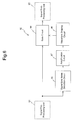
noise canceller 92 comprises (i) a signal line noise detection (SLND)circuit 96 which detects a noise component in the input signal from the signal pre-processingunit 91, (ii) anamplification circuit 97 which amplifies the noise signal detected by the signal linenoise detection circuit 96, (iii) awaveform shaping circuit 98 which outputs a gate control signal whose level changes according to whether or not the result of amplification by theamplification circuit 92 is greater than or equal to a predetermined magnitude, and (iv) agate circuit 99 which controls whether or not the signal from the signal pre-processingunit 91 is outputted just as it is or not, according to the level of the gate control signal from thewaveform shaping circuit 98. - Here, if the
receiving device 90 is a radio receiver, then the signal linenoise detection circuit 96 is built to include a high pass filter, since it is required to eliminate the high frequency noise component in thenoise canceller 92. Furthermore, thewaveform shaping circuit 98 includes a rectification circuit which rectifies the result of amplification by theamplification circuit 97, and a comparison circuit which decides whether or not the level of the rectified signal which is the result of rectification by the rectification circuit is greater than or equal to a reference voltage. Due to this, the gate control signal goes to the gate blocking level in periods in which the amplitude of the high frequency component in the input signal from the signal pre-processingunit 91 is large, while the gate control signal goes to gate open level the gate control signal goes to the gate open level in periods in which the amplitude of the high frequency component in the input signal from the signal pre-processingunit 91 is small. It should be understood that a technique has also been proposed in which, in order reliably to eliminate noise in pulse form, the periods in which the gate control signal goes to the gate blocking level are changed according to the conditions of reception of the broadcast waves (refer to Patent Document #1). - Moreover the
gate circuit 99 includes a sample and hold circuit, and, along with outputting the signal from the signal pre-processingunit 91 just as it is without alteration when the gate control signal is at the gate open level, also is adapted, when the gate control signal is at the gate blocking level, continuously to output the signal level from the signal pre-processingunit 91 directly before the gate control signal went to the gate blocking level. It should be understood that a technique has also been proposed in which change in the level of the signal from the signal pre-processingunit 91 while the gate control signal is at the gate blocking level is forecast by the gate circuit, and a signal which indicates the forecast change is outputted (refer to Patent Document #2). - Patent Document #1:
Japanese Laid-Open Patent Publication H8-56168
Patent Document #2:Japanese Laid-Open Patent Publication 2003-69435 - The techniques of the above described prior art examples are ones which perform elimination of noise components based upon the input signal to the noise canceller, and which excel from the point of view of performing elimination of noise components in pulse form in a simple manner. However, the noise component which is superimposed upon the input signal to the noise canceller is not limited to being a noise component in pulse form; for example, when the receiving device is a radio receiver, sometimes it is not possible to distinguish between the modulation component and the noise component in the broadcast wave.
- Furthermore, in the case of an onboard radio receiver or the like, there is a tendency towards increase of the types and the number of electrical equipment disposed around the receiver, which are electrically operated devices, and accordingly the amount of noise originating in the operation of this electrical equipment also tends to increase. In order to cope with this tendency, it has been considered to lower the reference voltage of the
waveform shaping circuit 98 of the above describednoise canceller 92, or the like, so as to increase the noise cancellation sensitivity of thenoise canceller 92. However, if the noise cancellation sensitivity is simply increased, then the rate of occurrence is increased of the state of affairs in which a component which properly ought to be passed through thenoise canceller 92, such as the modulation component in the broadcast wave and so on, also comes to be eliminated, which is undesirable. - The present invention has been conceived in consideration of the circumstances described above, and it takes it as its object to provide a noise canceller which can eliminate the noise component in the input signal in a logical manner.
- The noise canceller of the present invention is a noise canceller which eliminates a noise component included in an input signal comprising: a signal line noise detection means which detects a component included in said input signal which is estimated as being noise; a noise environment detection means which detects the operational state of at least one of electrical devices which could constitute a cause for superimposition of noise upon said input signal; a correction means which corrects the result of detection by said signal line noise detection means, using the result of detection by said noise environment detection means; and a noise elimination means which eliminates a noise component included in an input signal, based upon the result of correction by said correction means.
- With this noise canceller, the signal line noise detection means detects a component included in the input signal to the noise canceller which is estimated as being noise. At the same time as this detection of a component which is estimated as being noise, the noise environment detection means detects the operational state of electrical devices which could constitute a cause for superimposition of noise upon said input signal, for example of the electrical devices which are arranged adjacent to the receiving device. The correction means corrects the result of detection by the signal line noise detection means, using the result of detection by the noise environment detection means. Moreover, the noise elimination means eliminates a noise component included in the input signal, based upon the result of correction by said correction means obtained in this manner. As a result, noise elimination is performed while changing the noise cancellation sensitivity according to the result of detection of the noise environment, i.e. of the operational state of the electrical device which is provided adjacent to the receiving device.
- With the noise canceller of the present invention, said noise environment detection means may be adapted to detect noise upon a power supply line for supply of electrical power for the operation of said electrical device; and said noise environment detection means may also be adapted to detect change of an electrical current flowing in a power supply line for supply of electrical power for the operation of said electrical device. Here, the correction means may be adapted to perform weighted addition of the result of detection by said noise environment detection means and the result of detection by said signal line noise detection means.
- Furthermore, with the noise canceller of the present invention, the noise environment detection means may be adapted to detect whether or not each of said electrical devices is powered up. And here, the correction means may be adapted to add amounts corresponding to those ones among said electrical devices which are powered up, to the result of detection by said signal line noise detection means.
-
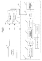
- Fig. 1 is a figure schematically showing the configuration of a radio receiver which incorporates a noise canceller according to a first embodiment of the present invention, also showing the configuration peripheral thereto;
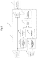
- Fig. 2 is a figure for explanation of the configuration of the noise canceller of Fig. 1;
- Fig. 3 is a figure schematically showing the configuration of a radio receiver which incorporates a noise canceller according to a second embodiment of the present invention, also showing the configuration peripheral thereto;
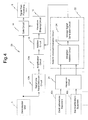
- Fig. 4 is a figure for explanation of the configuration of the noise canceller of Fig. 3;
- Fig. 5 is a figure schematically showing the configuration of an example of a receiving device according to the prior art; and
- Fig. 6 is a figure for explanation of the configuration of the prior art noise canceller of Fig. 5.
- In the following, a first embodiment of the present invention will be explained with reference principally to Figs. 1 and 2.
- In Fig. 1, there is shown the configuration of an
onboard radio receiver 10 which is equipped with a noise canceller according to the first embodiment of the present invention, and the configuration of certain devices peripheral to theradio receiver 10 is also shown. As shown in Fig. 1, a DC power supply device 81 (a battery or the like) and various items of electrical equipment 821, 822, ... which are electrical devices are disposed peripheral to this radio receiver. - This
radio receiver 10 comprises: (a) an antenna; (b) a radiofrequency amplification unit 2 which amplifies a signal induced in theantenna 1; (c) atuning unit 9 for the user to perform channel tuning; (d) alocal oscillation unit 8 which oscillates to produce a signal of a frequency corresponding to the result of channel tuning in thetuning unit 9; and (e) a mixer unit 3 which mixes together the result of amplification by the radiofrequency amplification unit 2 and the signal generated by thelocal oscillation unit 8. Here, frequency conversion from the signal at the frequency of the broadcast wave to a signal at an intermediate frequency is performed by thelocal oscillation unit 8 and the mixer unit 3. - Furthermore, the
radio receiver 10 comprises: (f) an intermediatefrequency amplification unit 4 which amplifies the intermediate frequency signal from the mixer unit 3; and (g) ademodulation unit 5 which performs detection (AM detection or FM detection) of the signal from the intermediatefrequency amplification unit 4 It should be understood that, if thisradio receiver 10 is an FM radio receiver, the intermediate frequency alsoamplification unit 4 includes an amplitude limitation circuit (a limiter). - Yet further, this
radio receiver 10 comprises: (h) a power supply line noise detection circuit (PLND) 12P which detects noise voltage fluctuation upon the power supply line; and (i) a noise cancellermain unit 11 which eliminates the noise component included in the signal detected by thedemodulation unit 5 while referring to the result of detection by the power supply linenoise detection circuit 12P. Here, the power supply linenoise detection circuit 12P is disposed adjacent to a terminal of the DCpower supply device 81 which supplies electrical power for operation. It should be understood that the noise canceller 19 (refer to Fig. 2) consists of the power supplynoise detection circuit 12P and the noise cancellermain unit 11. The configuration of thisnoise canceller 19 will be described in detail hereinafter. - Even further, this
radio receiver 10 comprises: (j) asignal post-processing unit 6 which processes the output signal from the noise cancellermain unit 11. If theradio receiver 10 is an FM stereo receiver, then thissignal post-processing unit 6 comprises a stereo demodulation circuit, a de-emphasis circuit, a low frequency amplification circuit, speakers, and the like. Furthermore, if theradio receiver 10 is an FM monaural receiver, then thissignal post-processing unit 6 comprises a de-emphasis circuit, a low frequency amplification circuit, a speaker, and the like. Moreover, if theradio receiver 10 is an AM receiver, then thissignal post-processing unit 6 comprises a low frequency amplification circuit, a speaker, and the like. - The power supply line
noise detection circuit 12P comprises a high pass filter. This is due to the fact that the power supply line noise which is generated in accompaniment with the operation of the electrical equipment items 821, 822, ... is high frequency noise. It should be understood that it is supposed that the power supply line noise which is due to the operation of theradio receiver 10 is quite low. Furthermore, if it is decided that there is a correlation between the magnitude of the component in some specified frequency band of the power supply line noise, and the magnitude of the noise component included in the signal which is the result of detection by thedemodulation unit 5, then it is desirable for the power supply linenoise detection circuit 12P to include a band pass filter which passes through a signal of that specified frequency band. - As shown in Fig. 2, the noise canceller
main unit 11 comprises: (i) a signal linenoise detection circuit 12N which detects a component in the input signal from thedemodulation unit 5 which it estimates to be noise; and (ii) anamplification circuit 13N which amplifies the result of detection by this signal linenoise detection circuit 12N. Here, this signal linenoise detection circuit 12N andamplification circuit 13N are constructed in a manner which is similar to that of the signal linenoise detection circuit 96 and theamplification circuit 97 of the prior art example described above. It should be understood that it will be supposed that the signal amplification ratio of theamplification circuit 13N is K0. - Furthermore, the noise canceller
main unit 11 comprises: (iii) anamplification circuit 13P which amplifies the power supply line noise signal which has been detected by the power supply linenoise detection circuit 12P; and (iv) anaddition circuit 14 which adds together the output signal from theamplification circuit 13N and the output signal from theamplification circuit 13P. Here if there is a possibility that, due to the addition calculation by theaddition circuit 14, accidental mutual cancellation between the output signal from theamplification circuit 13N and the output signal from theamplification circuit 13P may occur in the long term, then it is desirable for theamplification circuit 13P to include a rectification circuit which rectifies the result of its amplification. It should be understood that the ratio between the amplification ratio K1 and the signal amplification ratio K0 of the above describedamplification circuit 13N is determined by experiment or simulation or the like, from the point of view of elimination of the noise component by theentire noise canceller 19 in a logical manner. - Furthermore, the noise canceller
main unit 11 comprises: (v) awaveform shaping circuit 15 which changes the level of the gate control signal and outputs it, according as to whether or not the result of addition by theaddition circuit 14 is greater than or equal to a predetermined magnitude; and (vi) agate circuit 16 which controls whether or not the signal from thedemodulation unit 5 is outputted just as it is, according to the level of the gate control signal from thewaveform shaping circuit 15. Here, thiswaveform shaping circuit 15 andgate circuit 16 are constructed in a manner which is similar to that of thewaveform shaping circuit 98 andgate circuit 99 of the prior art example described above. - Next, the signal processing performed by the
radio receiver 10 having the configuration described above will be explained, with emphasis being principally directed upon the operation of elimination of the noise component by thenoise canceller 19. - The signal which is induced in the
antenna 1 by the received broadcast waves and the like, after being amplified by the radiofrequency amplification unit 2, is mixed with the local oscillation signal by the mixer unit 3 and is frequency converted to an intermediate frequency. The intermediate frequency signal which has been obtained in this manner is detected by thedemodulation unit 5, after having been amplified by the intermediatefrequency amplification unit 4. And the signal which is the result of this detection by thedemodulation unit 5 is inputted to the noise cancellermain unit 11. - In parallel with the processing of the signal induced in the
antenna 1 in this manner, the noise voltage in the power supply line is detected by the power supply linenoise detection circuit 12P. Here, if none of the items of electrical equipment 821, 822, ... is connected to electrical power so that none of these items of electrical equipment 821, 822, ... is operating, then the result of amplification by theamplification circuit 13P is presumably small, since the result of detection by the power supply linenoise detection circuit 12P is quite small. As a result, the result of the addition by theaddition circuit 14 is almost equal to the result of detection by the signal linenoise detection circuit 12N and amplification by theamplification circuit 13N. Due to this, if none of the items of electrical equipment 821, 822, ... is operating, then elimination of the noise component is performed by this noise canceller 19 with a similar noise cancellation sensitivity to that in the case of the prior art example described above. - If connection of at least one of the items of electrical equipment 821, 822, ... to the electrical power is commenced, then, when this item of electrical equipment 821, 822, ... which has been connected to the electrical power operates, a power supply line noise will be generated corresponding to the mode of operation thereof. The voltage change of the power supply line noise created in this manner is detected by the power supply line
noise detection circuit 12P, and is amplified by theamplification circuit 13P. The result of this amplification by theamplification circuit 13P is added by theaddition circuit 14 to the result of amplification by theamplification circuit 13N after detection by the signal linenoise detection circuit 12N. In other words, the result of addition by theaddition circuit 14 is a value which takes into consideration the operation of the item or item of electrical equipment 821, 822, ..., which could become a source of noise mixed into the signal from the radio receiver 10 (in particular, into the signal from the antenna 1). - After rectification of the result of addition obtained in this manner, the
waveform shaping circuit 15 compares together the level of this rectification result and a reference voltage. If the level of the result of rectification is less than the reference voltage, then thewaveform shaping circuit 15 outputs a gate control signal which is set to the gate open level. On the other hand, if the level of the result of rectification is greater than or equal to the reference voltage, then thewaveform shaping circuit 15 outputs a gate control signal which is set to the gate blocking level. - The
gate circuit 16 determines the mode of the output signal to thesignal post-processing unit 6 according to the level of the gate control signal which is outputted in this manner from thewaveform shaping circuit 15. In other words, if the gate control signal is at the gate open level, then thegate circuit 16 outputs the signal from thedemodulation unit 5 just as it is. Furthermore, if the gate control signal is at the gate blocking level, then thegate circuit 16 continues to output the signal level from thedemodulation unit 5 directly before the gate control signal went to the gate blocking level. - As explained above, with the
noise canceller 19 of this embodiment, the signal linenoise detection circuit 12N detects the estimated noise component included in the input signal to the noise cancellermain unit 11. At the same time as this estimated noise component is being detected, the power supply linenoise detection circuit 12P detects the power supply line noise voltage. This power supply line noise voltage reflects the so called noise environment due to the operational state of the various items of electrical equipment 821, 822, ... which can constitute sources of noise mixed into the signal from theantenna 1 and so on, and by extension reflects the probability of superimposition of noise upon the output signal from thedemodulation unit 5. - The result of detection by the signal line
noise detection circuit 12N and the result of detection by the power supply linenoise detection circuit 12P, which have been obtained in this manner, are added together with weightings by theamplification circuits addition circuit 14. The noise component which is included in the input signal to the noise cancellermain unit 11 is eliminated by the operation of thegate circuit 16, according to the level of the gate control signal generated by thewaveform shaping circuit 15 based upon the above result. - In other words, the noise cancellation sensitivity by the
noise canceller 19 is changed according to the result of detection of the noise environment by the power supply linenoise detection circuit 12P. Accordingly, with thenoise canceller 19 of this embodiment, it is possible to eliminate the noise component in the input signal in a logical manner. - It should be understood that although, in the first embodiment described above, the noise environment in the input signal to the
noise canceller 19 is detected by detecting the noise voltage upon the power supply line, it would also be possible to arrange to perform this detection by detecting change of the current flow amount flowing out from the DCpower supply device 81. In this case, it would be sufficient to insert a low resistance in the power supply line from the DCpower supply device 81, and to input the voltage generated between the two ends of this low resistance to theamplification circuit 13P described above. It should be understood that in this case, from the point of view of elimination of the noise component by theentire noise canceller 19 in a logical manner, the amplification ratio of theamplification circuit 13P would be determined by experiment or by simulation or the like, just as in the case of the first embodiment described above. - Furthermore although, in the above described first embodiment, it was arranged for the
amplification circuit 13P to be arranged within the noise cancellermain unit 11, if it is easy for noise to become mixed into the signal path from the power supply linenoise detection circuit 12P to theamplification circuit 13P, then it is desirable to provide a configuration in which theamplification circuit 13P is arranged as closely approached to the power supply linenoise detection circuit 12P. - In the following, a second embodiment of the present invention will be explained with reference principally to Figs. 3 and 4. It should be understood that, in the following explanation, to elements which are the same as or equivalent to ones of the first embodiment described above, the same reference symbols will be affixed, and duplicated explanation will be omitted.
- Fig. 3 schematically shows the configuration of an
onboard radio receiver 20 which incorporates anoise canceller 29 according to a second embodiment of the present invention, and also shows the configuration peripheral to this radio received 20. As shown in Fig. 3, as compared to theradio receiver 10 described above, thisradio receiver 20 differs only in the aspect that it comprises anoise canceller 29, instead of thenoise canceller 19. Furthermore, the electrical equipment which is disposed in the vicinity of theradio receiver 20 differs from that in the case of the first embodiment in the aspect that it consists of items of electrical equipment 831, 832, ..., each of which notifies thenoise canceller 29 of the fact that it is being powered (hereinafter this will be also termed "powered-up notification"). - As shown in Fig. 4, as compared to the
noise canceller 19 described above, thisnoise canceller 29 differs in the aspect that, instead of the power supply linenoise detection circuit 12P and theamplification circuit 13P, it comprises areception circuit 21 which receives a powered-up notification from each of the items of electrical equipment 831, 832, ..., and a noiseenvironment evaluation circuit 22. This noiseenvironment evaluation circuit 22 comprises: (i) aweighted addition circuit 23 which, along with allocating a weighting determined in advance to each of the items of electrical equipment which has issued a powered-up notification based upon the result of reception by thereception circuit 21, also allocates a weighting of zero to each of these items of electrical equipment which has not issued a powered-up notification, and adds these weighted values all together; and (ii) a voltagesignal generation circuit 24 which generates a voltage signal corresponding to the result of addition by theweighted addition circuit 23. - Here, the weightings which are allocated by the
weighted addition circuit 23 to each of the items of electrical equipment 831, 832, ... are determined in relation to the amounts of noise superimposed upon the signal output from thedemodulation unit 5 due to the operation of the corresponding one of the items of electrical equipment 831, 832, ..., based upon experiment or simulation. Furthermore, the conversion coefficient in the voltagesignal generation circuit 24 from the result of addition by theweighted addition circuit 23 to its output voltage value is determined by experiment or simulation or the like, from the point of view of elimination of the noise component by theentire noise canceller 29 in a logical manner. It should be understood that, if none of the items of electrical equipment 831, 832, ... issues a powered-up notification, so that the result of addition by theweighted addition circuit 23 is zero, then it is arranged for a voltage signal of 0 V to be outputted from the voltagesignal generation circuit 24. - Next, the signal processing performed by the
radio receiver 20 having the configuration described above will be explained, with emphasis being principally directed upon the operation of elimination of the noise component by thenoise canceller 29. - In a manner similar to the case with the first embodiment, a signal which has been induced in the
antenna 1 due to reception of a broadcast wave or the like is mixed with a local oscillation signal by the mixer unit, after having been amplified by the radiofrequency amplification unit 2, and is thereby frequency converted to an intermediate frequency. The intermediate frequency signal which has been obtained in this manner is detected by thedemodulation unit 5, after having been amplified by the intermediatefrequency amplification unit 4. The signal which results from this detection by thedemodulation unit 5 is inputted to thenoise canceller 29. - In parallel with the processing in this manner of the signal which has been induced in the
antenna 1, the power up notifications from each one of the items of electrical equipment 831, 832, ... which is powered up are supplied to thenoise canceller 29. In thenoise canceller 29, thereception circuit 21 which is provided before the noiseenvironment evaluation circuit 22 receives these powered-up notifications. The results of reception by thereception circuit 21 are received by theweighted addition circuit 23. Here, if none of the items of electrical equipment 831, 832, ... is powered up, so that no such powered-up notifications are present, then, since the result of addition by theweighted addition circuit 23 as described above is zero, a voltage signal of 0 V is outputted from the voltagesignal generation circuit 24. As a result, the result of addition by theaddition circuit 14 becomes the same as the result of detection by the signal linenoise detection circuit 12N and amplification by theamplification circuit 13N; and accordingly, due to this, just as in the case of the first embodiment described above, if none of the items of electrical equipment 831, 832, ... is powered up, then elimination of the noise component is performed by this noise canceller 29 with a similar noise cancellation sensitivity to that in the case of the prior art example described above. - If connection of at least one of the items of electrical equipment 821, 822, ... to the electrical power is commenced, then, when this at least one item of electrical equipment 821, 822, ... which has been connected to the electrical power operates, a powered-up notification is issued from this at least one item of electrical equipment 821, 822, .... In this case, after a weighting which is determined in advance has been allocated by the
weighted addition circuit 23 to each of the items of electrical equipment which is powered up in the manner described above, these values are then all added together. A voltage signal of a voltage value which corresponds to the result of this addition by theweighted addition circuit 23 is generated by the voltagesignal generation circuit 24. The voltage signal which is outputted from the voltagesignal generation circuit 24 is added by theaddition circuit 14 to the result of amplification by theamplification circuit 13N after detection by the signal linenoise detection circuit 12N. In other words, the result of addition by theaddition circuit 14 is a value which takes into consideration the operation of the item or item of electrical equipment 821, 822, ..., which could become a source of noise mixed into the signal from the radio receiver 10 (in particular, into the signal from the antenna 1). - In a similar manner to the case for the result of addition by the
addition circuit 14 in the first embodiment, waveform shaping is performed by thewaveform shaping circuit 15, and is inputted to thegate circuit 16 as a gate control signal. Thegate circuit 16 determines the mode of the output signal to thesignal post-processing unit 6 according to the level of the gate control signal, in a manner similar to the case in the first embodiment. - As explained above, with the
noise canceller 29 of this embodiment, the noiseenvironment evaluation circuit 22 receives a powered-up notification from each of the items of electrical equipment 831, 832, ..., and generates a voltage signal of a voltage value which reflects the noise environment due to those items of electrical equipment which are powered up. The voltage signal which is obtained in this manner is added by theaddition circuit 14 to the result of detection by the signal line noise detection circuit 12n and amplification by theamplification circuit 13N. The noise component included in the input signal to thenoise canceller 29 is eliminated, due to the operation of thegate circuit 16 corresponding to the level of a gate control signal which is generated by thewaveform shaping circuit 15 based upon this result. - In other words, the noise cancellation sensitivity by the
noise canceller 29 is changed according to the result of evaluation by the noiseenvironment evaluation circuit 22. Accordingly, with thenoise canceller 29 of this embodiment, it is possible to eliminate the noise component in the input signal in a logical manner. - It should be understood that, in the second embodiment described above, it was arranged to issue a powered-up notification from each of the items of electrical equipment 831, 832, .... By contrast it would also be possible, along with disposing various items of electronic equipment 821, 822, ... in the vicinity of the
radio receiver 20 in a similar manner to the case in the first embodiment, also to arrange to detect whether each of these items of electrical equipment 821, 822, ... is powered up or not, by detecting the electrical current which is flowing from the DCpower supply device 81 to each of these items of electrical equipment 821, 822. - Furthermore, in the second embodiment described above, it was arranged for digitally weighed addition to be performed by the noise
environment evaluation circuit 22, and for a voltage corresponding to the result of this addition to be generated using some type of digital-analog converter (DAC). By contrast, it would also be possible to arrange, along with generating a voltage signal of a specific voltage value for each of the items of electrical equipment 831, 832, ... if that item of electrical equipment 831, 832, ... has issued a powered-up notification, also to output the result of adding together these voltage signals to theaddition circuit 14. - It should be understood that, although in the first and second embodiments described above the present invention was applied to a noise canceller mounted to an onboard radio receiver, of course it would also be possible to apply the present invention to a noise canceller which is mounted to some other type of signal processing device.
Claims (7)
- A noise canceller which eliminates a noise component included in an input signal comprising:a signal line noise detection means which detects a component included in said input signal which is estimated as being noise;a noise environment detection means which detects the operational state of at least one of electrical devices which could constitute a cause for superimposition of noise upon said input signal;a correction means which corrects the result of detection by said signal line noise detection means, using the result of detection by said noise environment detection means; anda noise elimination means which eliminates a noise component included in an input signal, based upon the result of correction by said correction means.
- A noise canceller as described in Claim 1, wherein
said noise environment detection means detects noise upon a power supply line for supply of electrical power for the operation of said electrical device. - A noise canceller as described in Claim 2, wherein
said correction means performs weighted addition of the result of detection by said noise environment detection means and the result of detection by said signal line noise detection means. - A noise canceller as described in Claim 1, wherein
said noise environment detection means detects change of an electrical current flowing in a power supply line for supply of electrical power for the operation of said electrical device. - A noise canceller as described in Claim 4, wherein
said correction means performs weighted addition of the result of detection by said noise environment detection means and the result of detection by said signal line noise detection means. - A noise canceller as described in Claim 1, wherein
said noise environment detection means detects whether or not each of said electrical devices1 is powered up. - A noise canceller as described in Claim 6, wherein
said correction means adds amounts corresponding to those ones among said electrical devices which are powered up, to the result of detection by said signal line noise detection means.
Applications Claiming Priority (2)
| Application Number | Priority Date | Filing Date | Title |
|---|---|---|---|
| JP2005117589 | 2005-04-14 | ||
| PCT/JP2006/307474 WO2006112280A1 (en) | 2005-04-14 | 2006-04-07 | Noise canceler |
Publications (1)
| Publication Number | Publication Date |
|---|---|
| EP1871011A1 true EP1871011A1 (en) | 2007-12-26 |
Family
ID=37115006
Family Applications (1)
| Application Number | Title | Priority Date | Filing Date |
|---|---|---|---|
| EP06731421A Withdrawn EP1871011A1 (en) | 2005-04-14 | 2006-04-07 | Noise canceler |
Country Status (3)
| Country | Link |
|---|---|
| EP (1) | EP1871011A1 (en) |
| JP (1) | JP4177437B2 (en) |
| WO (1) | WO2006112280A1 (en) |
Cited By (3)
| Publication number | Priority date | Publication date | Assignee | Title |
|---|---|---|---|---|
| US20100244817A1 (en) * | 2009-03-25 | 2010-09-30 | Aisan Kogyo Kabushiki Kaisha | Resolver |
| US9100081B2 (en) | 2010-03-18 | 2015-08-04 | Panasonic Intellectual Property Management Co., Ltd. | Radio reception device for vehicle and noise cancellation method |
| EP3637800A1 (en) * | 2018-10-12 | 2020-04-15 | Oticon A/s | Noise reduction method and system |
Families Citing this family (1)
| Publication number | Priority date | Publication date | Assignee | Title |
|---|---|---|---|---|
| JP2010245749A (en) * | 2009-04-03 | 2010-10-28 | Panasonic Corp | Noise canceling unit and high frequency receiving unit using the same |
Family Cites Families (3)
| Publication number | Priority date | Publication date | Assignee | Title |
|---|---|---|---|---|
| JP2760240B2 (en) * | 1992-03-11 | 1998-05-28 | 松下電器産業株式会社 | Noise suppression device |
| JP3010465B2 (en) * | 1994-10-14 | 2000-02-21 | 松下電器産業株式会社 | Noise suppression device |
| JPH08335915A (en) * | 1995-06-08 | 1996-12-17 | Matsushita Electric Ind Co Ltd | Electromagnetic interference removal method |
-
2006
- 2006-04-07 WO PCT/JP2006/307474 patent/WO2006112280A1/en not_active Ceased
- 2006-04-07 EP EP06731421A patent/EP1871011A1/en not_active Withdrawn
- 2006-04-07 JP JP2007521185A patent/JP4177437B2/en not_active Expired - Fee Related
Non-Patent Citations (1)
| Title |
|---|
| See references of WO2006112280A1 * |
Cited By (7)
| Publication number | Priority date | Publication date | Assignee | Title |
|---|---|---|---|---|
| US20100244817A1 (en) * | 2009-03-25 | 2010-09-30 | Aisan Kogyo Kabushiki Kaisha | Resolver |
| US9100081B2 (en) | 2010-03-18 | 2015-08-04 | Panasonic Intellectual Property Management Co., Ltd. | Radio reception device for vehicle and noise cancellation method |
| EP3637800A1 (en) * | 2018-10-12 | 2020-04-15 | Oticon A/s | Noise reduction method and system |
| US11178480B2 (en) | 2018-10-12 | 2021-11-16 | Oticon A/S | Noise reduction method and system |
| US11849275B2 (en) | 2018-10-12 | 2023-12-19 | Oticon A/S | Noise reduction method and system |
| EP4346129A3 (en) * | 2018-10-12 | 2024-09-25 | Oticon A/s | Noise reduction method and system |
| US12273678B2 (en) | 2018-10-12 | 2025-04-08 | Oticon A/S | Noise reduction method and system |
Also Published As
| Publication number | Publication date |
|---|---|
| WO2006112280A1 (en) | 2006-10-26 |
| JPWO2006112280A1 (en) | 2008-12-11 |
| JP4177437B2 (en) | 2008-11-05 |
Similar Documents
| Publication | Publication Date | Title |
|---|---|---|
| US6327313B1 (en) | Method and apparatus for DC offset correction | |
| US7317774B2 (en) | Systems and methods for reducing harmonic interference effects in analog to digital conversion | |
| US7885628B2 (en) | FM tuner | |
| US9100081B2 (en) | Radio reception device for vehicle and noise cancellation method | |
| US7486941B2 (en) | Method and apparatus for dynamic gain and phase compensations | |
| CN102163978A (en) | Broadcast receiving apparatus and method of determining presence of noise performed by broadcast receiving apparatus | |
| GB2315966A (en) | Received signal strength detecting circuit | |
| US20040176056A1 (en) | Single-tone detection and adaptive gain control for direct-conversion receivers | |
| US20090298454A1 (en) | Receiver | |
| US20080279393A1 (en) | Noise Eliminating Circuit | |
| WO2006106788A1 (en) | Reducing apparatus and method, and receiving apparatus | |
| JP4177437B2 (en) | Noise canceller | |
| US9698802B2 (en) | Method for amplifying an echo signal suitable for vehicle surroundings detection and device for carrying out the method | |
| US20080096511A1 (en) | Method and apparatus for minimizing noise on a power supply line of a mobile radio | |
| JP5074279B2 (en) | Signal processing device | |
| US7072617B1 (en) | System and method for suppression of RFI interference | |
| US7049884B2 (en) | Demodulation arrangement for a radio signal | |
| US6700443B2 (en) | Reduction of sensitivity of an amplifier to an offset voltage | |
| EP1865609A1 (en) | Signal attenuating circuit | |
| CN100559723C (en) | Receiving module and receiving unit using the receiving module | |
| JP3570378B2 (en) | Noise removal device and audio device | |
| EP1968202B1 (en) | Reception sensitivity determining apparatus | |
| JP4693667B2 (en) | Unwanted wave detector | |
| US20090124228A1 (en) | Intermodulation disturbance detecting unit | |
| JPH1041840A (en) | Receiver |
Legal Events
| Date | Code | Title | Description |
|---|---|---|---|
| PUAI | Public reference made under article 153(3) epc to a published international application that has entered the european phase |
Free format text: ORIGINAL CODE: 0009012 |
|
| 17P | Request for examination filed |
Effective date: 20071105 |
|
| AK | Designated contracting states |
Kind code of ref document: A1 Designated state(s): AT BE BG CH CY CZ DE DK EE ES FI FR GB GR HU IE IS IT LI LT LU LV MC NL PL PT RO SE SI SK TR |
|
| DAX | Request for extension of the european patent (deleted) | ||
| RAP1 | Party data changed (applicant data changed or rights of an application transferred) |
Owner name: PIONEER CORPORATION |
|
| STAA | Information on the status of an ep patent application or granted ep patent |
Free format text: STATUS: THE APPLICATION IS DEEMED TO BE WITHDRAWN |
|
| 18D | Application deemed to be withdrawn |
Effective date: 20121101 |