EP1865761A2 - Electronic appliance - Google Patents
Electronic appliance Download PDFInfo
- Publication number
- EP1865761A2 EP1865761A2 EP07010993A EP07010993A EP1865761A2 EP 1865761 A2 EP1865761 A2 EP 1865761A2 EP 07010993 A EP07010993 A EP 07010993A EP 07010993 A EP07010993 A EP 07010993A EP 1865761 A2 EP1865761 A2 EP 1865761A2
- Authority
- EP
- European Patent Office
- Prior art keywords
- antistatic paint
- electrically conductive
- static electricity
- protective panel
- painted
- Prior art date
- Legal status (The legal status is an assumption and is not a legal conclusion. Google has not performed a legal analysis and makes no representation as to the accuracy of the status listed.)
- Granted
Links
- 239000003973 paint Substances 0.000 claims abstract description 111
- 230000001681 protective effect Effects 0.000 claims abstract description 68
- 230000005611 electricity Effects 0.000 claims abstract description 57
- 230000003068 static effect Effects 0.000 claims abstract description 57
- 239000000126 substance Substances 0.000 claims description 36
- 239000002184 metal Substances 0.000 claims description 21
- 238000007599 discharging Methods 0.000 claims description 2
- 230000001413 cellular effect Effects 0.000 abstract description 20
- 239000004973 liquid crystal related substance Substances 0.000 abstract description 15
- 208000028659 discharge Diseases 0.000 description 21
- 238000004040 coloring Methods 0.000 description 13
- 239000000843 powder Substances 0.000 description 11
- 230000000694 effects Effects 0.000 description 4
- 238000010422 painting Methods 0.000 description 4
- OKTJSMMVPCPJKN-UHFFFAOYSA-N Carbon Chemical compound [C] OKTJSMMVPCPJKN-UHFFFAOYSA-N 0.000 description 2
- 239000004925 Acrylic resin Substances 0.000 description 1
- 229920000178 Acrylic resin Polymers 0.000 description 1
- 229910052799 carbon Inorganic materials 0.000 description 1
- 230000015556 catabolic process Effects 0.000 description 1
- 238000005401 electroluminescence Methods 0.000 description 1
- 238000005516 engineering process Methods 0.000 description 1
- 229910002804 graphite Inorganic materials 0.000 description 1
- 239000010439 graphite Substances 0.000 description 1
- 238000012986 modification Methods 0.000 description 1
- 230000004048 modification Effects 0.000 description 1
- 229920001690 polydopamine Polymers 0.000 description 1
Images


Classifications
-
- H—ELECTRICITY
- H05—ELECTRIC TECHNIQUES NOT OTHERWISE PROVIDED FOR
- H05K—PRINTED CIRCUITS; CASINGS OR CONSTRUCTIONAL DETAILS OF ELECTRIC APPARATUS; MANUFACTURE OF ASSEMBLAGES OF ELECTRICAL COMPONENTS
- H05K9/00—Screening of apparatus or components against electric or magnetic fields
- H05K9/0067—Devices for protecting against damage from electrostatic discharge
-
- H—ELECTRICITY
- H05—ELECTRIC TECHNIQUES NOT OTHERWISE PROVIDED FOR
- H05K—PRINTED CIRCUITS; CASINGS OR CONSTRUCTIONAL DETAILS OF ELECTRIC APPARATUS; MANUFACTURE OF ASSEMBLAGES OF ELECTRICAL COMPONENTS
- H05K9/00—Screening of apparatus or components against electric or magnetic fields
- H05K9/0073—Shielding materials
- H05K9/0079—Electrostatic discharge protection, e.g. ESD treated surface for rapid dissipation of charges
-
- Y—GENERAL TAGGING OF NEW TECHNOLOGICAL DEVELOPMENTS; GENERAL TAGGING OF CROSS-SECTIONAL TECHNOLOGIES SPANNING OVER SEVERAL SECTIONS OF THE IPC; TECHNICAL SUBJECTS COVERED BY FORMER USPC CROSS-REFERENCE ART COLLECTIONS [XRACs] AND DIGESTS
- Y10—TECHNICAL SUBJECTS COVERED BY FORMER USPC
- Y10T—TECHNICAL SUBJECTS COVERED BY FORMER US CLASSIFICATION
- Y10T428/00—Stock material or miscellaneous articles
- Y10T428/24—Structurally defined web or sheet [e.g., overall dimension, etc.]
- Y10T428/24802—Discontinuous or differential coating, impregnation or bond [e.g., artwork, printing, retouched photograph, etc.]
- Y10T428/24893—Discontinuous or differential coating, impregnation or bond [e.g., artwork, printing, retouched photograph, etc.] including particulate material
- Y10T428/24909—Free metal or mineral containing
-
- Y—GENERAL TAGGING OF NEW TECHNOLOGICAL DEVELOPMENTS; GENERAL TAGGING OF CROSS-SECTIONAL TECHNOLOGIES SPANNING OVER SEVERAL SECTIONS OF THE IPC; TECHNICAL SUBJECTS COVERED BY FORMER USPC CROSS-REFERENCE ART COLLECTIONS [XRACs] AND DIGESTS
- Y10—TECHNICAL SUBJECTS COVERED BY FORMER USPC
- Y10T—TECHNICAL SUBJECTS COVERED BY FORMER US CLASSIFICATION
- Y10T428/00—Stock material or miscellaneous articles
- Y10T428/25—Web or sheet containing structurally defined element or component and including a second component containing structurally defined particles
Definitions
- the present invention relates to electronic appliances, and more particularly to electronic appliances that are so structured as to be resistant to static electricity.
- an electronic appliance such as a cellular phone or PDA (personal digital assistant)
- PDA personal digital assistant
- static electricity that builds up as the appliance is used is applied to it and enters its casing through a gap or the like in it
- the static electricity conducts to electronic components mounted on a circuit board inside the appliance, and may cause malfunctioning of electronic circuits and breakdown of electronic components.
- protective components such as diodes and resistors are fitted on the circuit board for protection against static electricity.
- this conventional mode of protecting against static electricity involves fitting extra protective components, and thus has the disadvantage of increasing the number of electronic components mounted on a circuit board.
- JP-A-H11-185991 proposes an electronic appliance comprising a circuit board having electronic components mounted thereon and a display panel, wherein a transparent electrically conductive sheet is laid over the surface of the display panel, and this transparent electrically conductive sheet is connected to a grounded portion of the circuit board with an electrically conductive member such as a coil spring. This makes it possible to achieve protection against static electricity without increasing the number of electronic components mounted on the circuit board.
- JP-A-S61-292879 proposes an electronic appliance wherein a pattern of electrically conductive ink is printed on the surface of a panel member formed of plastic, and the printed pattern is electrically connected to a metal chassis or the like. This too makes it possible to achieve protection against static electricity without increasing the number of electronic components mounted on a circuit board.
- the electronic appliance proposed in JP-A-H11-185991 mentioned above requires that a transparent electrically conductive sheet be laid over the display panel, and thus requires an extra space corresponding to the thickness of the transparent electrically conductive sheet inside the appliance. This makes it more difficult to secure a space in which to mount components inside the appliance, and thus makes it more difficult to make the appliance compact and slim.
- the transparent electrically conductive sheet laid over the display panel certainly offers the effect of shielding off noise generated from around the display panel, using a transparent electrically conductive sheet in a wireless communication appliance such as a cellular phone that generates radiowaves has, exactly because of the shielding effect of the sheet, the disadvantage of changing the wireless communication characteristics of the appliance.
- An object of the present invention is to provide an electronic appliance that permits protection of election components against static electricity with a minimum change in the wireless communication characteristics of the appliance and that achieves it with a minimum increase in the number of electronic components mounted on a base board to permit the appliance to be made compact and slim.
- an electronic appliance is provided with: a base board having electronic components mounted thereon; and a painted member painted with an antistatic paint that discharges static electricity but is electrically non-conductive.
- the electronic appliance according to the first aspect of the invention thanks to the above-described painted member painted with the antistatic paint that discharges static electricity, in a case where part of the painted member painted with the antistatic paint is connected to a grounded portion, static electricity that builds up during use can be diverted across the part of the painted member painted with the antistatic paint to the grounded portion.
- static electricity that builds up during use can be prevented from conducting to electronic components on the base board.
- the electronic components mounted on the base board can be protected from static electricity, and thus, the painted member painted with the antistatic paint helps achieve protection against static electricity in the appliance.
- the antistatic paint since the antistatic paint is electrically non-conductive, it does not exert, even in a case where the part painted with the antistatic paint is connected to a grounded portion, a shielding effect as exerted by a transparent electrically conductive sheet or an electrically conductive paint such as an electrically conductive ink. This helps minimize the change in the wireless communication specifications of the appliance. Hence, even in a wireless communication appliance such as a cellular phone that generates radiowaves, the painted member painted with the antistatic paint helps achieve protection against static electricity in the appliance.
- the painted member painted with the antistatic paint helps achieve protection against static electricity without requiring mounting of extra protective components (electronic components) such as diodes and resistors on the base board. This helps minimize the increase in the number of electronic components mounted on the base board, and thus helps secure a sufficiently large component mounting area on the base board.
- the painted member painted with the antistatic paint that discharges static electricity helps achieve protection against static electricity in the appliance with a paint that can be made thinner than a sheet member such as a transparent electrically conductive sheet. This makes it easy to secure inside the appliance a space in which to mount components, and thus permits the appliance to be made compact and slim.
- the electronic appliance according to the first aspect of the invention described above may be further provided with: a display panel for displaying information; and a protective panel for protecting the display panel.
- the painted member is, for example, the protective panel painted with the antistatic paint.
- the electronic appliance is an electrically conductive member that is grounded.
- the protective panel has formed thereon a discharge path for preferentially discharging static electricity.
- the discharge path is connected to or placed close to the electrically conductive member.
- the antistatic paint contains an electrically insulating base substance and an electrically conductive substance, and the antistatic paint is made electrically non-conductive as a result of the electrically conductive substance being discontinuously dispersed in the electrically insulating base substance.
- the antistatic paint can be made electrically non-conductive but simultaneously capable of passing static electricity by secondary discharge.
- the electrically insulating base substance is present between discontinuous parts of the electrically conductive substance, and this makes electrical conduction impossible; here, even though the electrically insulating base substance is embedded in the electrically conductive substance, so long as different parts of the electrically conductive substance are close enough together, static electricity passes by secondary discharge.
- the antistatic paint contains the highest possible content of the electrically conductive substance within the range in which the antistatic paint remains electrically non-conductive.
- the electrically conductive substance is a metal substance.
- the protective panel has the inner surface thereof painted with the antistatic paint.
- the protective panel can be fitted to the appliance such that the part of the former painted with the antistatic paint is located inside the latter.
- the part can easily be connected to or placed close to the electrically conductive member that is grounded.
- the user can be prevented from touching the part painted with the antistatic paint, and thus the paint can be prevented from being removed as a result of the user touching the part painted with the antistatic paint.
- the base board may have a grounded portion so that the electrically conductive member is grounded by being connected to or placed close to the grounded portion of the base board.
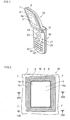
- Fig. 1 is an overall perspective view of a cellular phone according to a first embodiment of the invention
- Fig. 1 is an overall perspective view of a cellular phone according to a first embodiment of the invention.
- Fig. 2 is a schematic plan view of a display portion of the cellular phone according to the first embodiment of the invention.
- Fig. 3 is a cross-sectional view along line 100-100 in Fig. 2.
- Fig. 4 is a cross-sectional view of a protective panel along line 200-200 in Fig. 2.
- Fig. 5 is a conceptual cross-sectional view of an antistatic paint film in the cellular phone according to the first embodiment of the invention.
- the cellular phone according to the first embodiment is composed of a display portion 50 and an operation portion 60 that are foldably coupled together with a hinge portion 70.
- On the operation portion 60 are arranged a power key 21 for turning the power on and off, a plurality of numerical keys 22 for entering telephone numbers etc., a plurality of operation keys 23, and a cross key 24.
- On the display portion 50 is arranged a liquid crystal display panel 5 for displaying character-based information such as telephone numbers as well as image-based information.
- the display portion 50 is provided with a top casing 1, a bottom casing 2, a circuit board 4 having electronic components 3 mounted thereon, the liquid crystal display panel 5, and a protective panel 6.
- the circuit board 4 is one example of what is called “base board” in the present invention
- the liquid crystal display panel 5 is one example of what is called “display panel” in the present invention.
- the top casing 1 has an opening 1a, and has a recess 1b around the opening 1a.
- a plurality of (four) through holes 1c into which metal screws 7 are inserted, are formed at predetermined intervals.
- a recess 1d is formed with a diameter larger than the head of the screws 7.
- bosses 2a are formed each having a screw hole.
- through holes 4a are formed through which the screws 7 is inserted.
- the metal screws 7 are one example of what is called “electrically conductive member" in the present invention.
- the liquid crystal display panel 5 is arranged on the top side of the circuit board 4, in an area facing the opening 1a in the top casing 1.
- the protective panel 6 is fitted, which is formed of transparent acrylic resin.
- the protective panel 6 is fitted in the recess 1b in the top casing 1, and serves to protect the display surface of the liquid crystal display panel 5.
- the protective panel 6 is fitted on the top casing 1 such that the front surface (facing outward) of the protective panel 6 is substantially flush with the outer surface of the top casing 1.
- a frame-shaped sponge member 8 is fitted between the protective panel 6 and the liquid crystal display panel 5. The sponge member 8 prevents entry of foreign matter between the liquid crystal display panel 5 and the protective panel 6.
- the top casing 1, the circuit board 4, and the bottom casing 2 are put together in this order, and the screws 7 inserted through the through holes 1c in the top casing 1 are put through the through holes 4a in the circuit board 4 and fixed to the bosses 2a on the bottom casing 2.
- the recesses 1d around the through holes 1c in the top casing 1 are so formed that the heads of the screws 7 protrude from the floor surface of the recess 1b around the opening 1a.
- grounded portions 4b are formed that are kept at the ground-side potential of the supplied electric power.
- the grounded portions 4b make contact with or come close to the screws 7, and thereby permit the screws 7 to be grounded.
- a panel coloring paint film 9 for giving the protective panel 6 a desired color and an antistatic paint film 10 for protection against static electricity is formed on the surface of the protective panel 6 .
- the panel coloring paint film 9 is formed by painting a panel coloring paint that gives the protective panel 6 the color thereof.
- the antistatic paint film 10 is formed by painting an antistatic paint that lets static electricity pass across it but is electrically non-conductive.
- used as the antistatic paint is a paint for metallic coloring, such as a mirror ink.
- the antistatic paint has a metal powder 10b, as an electrically conductive substance, discontinuously dispersed in an electrically non-conductive base substance 10a.
- the electrically non-conductive base substance 10a is present between dispersed parts of the metal powder 10b.
- dispersed parts of the metal powder 10b remain close enough together to pass (discharge) static electricity by secondary discharge.
- the antistatic paint contains the highest possible content of the metal powder 10b within the range in which the antistatic paint remains electrically non-conductive.
- the panel coloring paint film 9 is formed over a predetermined area on the surface of the protective panel 6, excluding where a display window 6a (unpainted portion) is located to permit what is displayed on the liquid crystal display panel 5 to be viewed.
- the antistatic paint film 10 is formed over that predetermined area on the top surface of the panel coloring paint film 9. The antistatic paint film 10 thus forms a discharge path across which static electricity preferentially passes (is discharged).
- the panel coloring paint film 9 and the antistatic paint film 10 are formed on the inner surface (facing the inside of the appliance) of the protective panel 6.
- the heads of the screws 7 protruding from the floor surface of the recess 1b around the opening 1a make contact with or come close to the antistatic paint film 10 on the protective panel 6.
- the antistatic paint film 10 is simply located close to the heads of the screws 7, static electricity can be passed, by secondary discharge, to the screws 7, which are grounded.
- the antistatic paint film 10 on the protective panel 6 and the heads of the grounded screws 7 are kept in contact with or close to each other.
- static electricity that builds up during use can be diverted across the antistatic paint film 10 formed on the protective panel 6 via the metal screws 7 to the grounded portions 4b of the circuit board 4.
- static electricity can be prevented from conducting to the electronic components 3 on the circuit board 4.
- the electronic components 3 mounted on the circuit board 4 can be protected from static electricity.
- the antistatic paint film 10 is formed by painting the surface of the protective panel 6 with an antistatic paint that is electrically non-conductive.
- the antistatic paint film 10 on the protective panel 6 does not act as a shield as does a transparent electrically conductive sheet or an electrically conductive paint such as an electrically conductive ink. This helps minimize the change in the wireless communication specifications of the appliance.
- fitting it with the protective panel 6 having the antistatic paint film 10 formed thereon helps achieve protection against static electricity in the appliance.
- the antistatic paint contains, as an electrically conductive substance, the highest possible content of the metal powder 10b within the range in which the antistatic paint remains electrically non-conductive. This helps make the distances between discontinuous parts of the metal powder 10b dispersed in the base substance 10a as small as possible, and thus helps make secondary discharge of static electricity between discontinuous parts of the metal powder 10b easier.
- static electricity can easily be passed across the antistatic paint film 10 formed on the surface of the protective panel 6.
- it can easily be diverted via the screws 7, which are in contact with or close to the antistatic paint film 10, to the grounded portions 4b of the circuit board 4.
- the antistatic paint film 10 on the surface of the protective panel 6, it is possible to achieve protection against static electricity without a need to mount extra protective components (electronic components 3) such as diodes and resistors on the circuit board 4. This helps minimize the increase in the number of electronic components 3 mounted on the circuit board 4, and helps secure a sufficient mounting area on the circuit board 4.
- the protective panel 6 painted with the antistatic paint helps achieve protection against static electricity in the appliance with a paint that can be made thinner than a sheet member such as a transparent electrically conductive sheet. This makes it easy to secure inside the appliance a space in which to mount components, and thus permits the appliance to be made compact and slim.
- Fig. 6 is a schematic plan view of a display portion of a cellular phone according to a second embodiment of the invention.
- Fig. 7 is a cross-sectional view along line 300-300 in Fig. 6.
- metal coil springs 34 are used in the display portion 150.
- the structure here is the same as in the first embodiment described above, and therefore no overlapping explanations will be repeated.
- the top casing 31, the circuit board 33, and the bottom casing 32 are put together in this order.
- the top casing 31 has an opening 31 a, and has a recess 31b around the opening 31a.
- through holes 31c are formed vertically (in the direction of the thickness of the top casing 31).
- a grounded portion 33a is provided that is kept at the ground-side potential of the supplied electric power.
- the coil springs 34 are inserted into the through holes 31c in the top casing 31.
- the length of the coil springs 34 is greater than the depth of the through holes 31c, and thus, when the coil springs 34 are inserted into the through holes 31 c, the former protrude out of the latter.
- the coil springs 34 at one end thereof, make contact with the antistatic paint film 10 on the protective panel 6, and in addition the coil springs 34, at the other end thereof, make contact with the grounded portion 33a of the circuit board 33. That is, in the second embodiment, the antistatic paint film 10 on the protective panel 6 and the grounded portion 33a of the circuit board 33 are connected together by the coil springs 34.
- the coil springs 34 instead of the screws 7 (see Fig. 3), are used to connect the antistatic paint film 10 on the protective panel 6 and the grounded portion 33a of the circuit board 33 together. Accordingly, on the bottom casing 32, no bosses 2a (see Fig. 3) are formed that have screw holes to permit the screws 7 to be fixed thereto.
- the antistatic paint film 10 on the protective panel 6 and the grounded portion 33a of the circuit board 33 are connected together by the coil springs 34 so that static electricity that builds up during use is diverted across the antistatic paint film 10 on the protective panel 6 to the grounded portion 33a of the circuit board 33.
- static electricity is prevented from conducting to the electronic components 3 on the circuit board 33.
- the circuit board 4 is one example of what is called “base board” in the present invention
- the coil springs 34 are one example of what is called “electrically conductive member" in the present invention.
- the first and second embodiments described above deal with examples where the invention is applied to a cellular phone, this is in no way intended to limit the application of the invention; the invention may also be applied to electronic appliances other than a cellular phone, such as PHS (personal handy-phone system) phones, PDAs, and electronic still camera.
- PHS personal handy-phone system
- the electronic appliances to which the invention is applied may or may not be portable.
- the first and second embodiments described above deal with examples where an antistatic paint is applied to the surface of a protective panel, this is in no way intended to limit how the application is practiced; instead, the antistatic paint may be applied to any member other than a protective panel, such as the casing.
- the first and second embodiments described above deal with examples where an antistatic paint is applied to a protective panel for protecting the surface of a liquid crystal display panel, this is in no way intended to limit how the application is practiced; instead, the antistatic paint may be applied to any member other than a protective panel for protecting a liquid crystal display panel. In that case, the invention can be applied to an electronic appliance that has no display panel.
- any display panel other than a liquid crystal display panel may be used, such as an LED (light-emitting diode) display, an EL (electroluminescence) display, a PDP (plasma display panel), and a CRT (cathode ray tube).
- LED light-emitting diode
- EL electroluminescence
- PDP plasma display panel
- CRT cathode ray tube
- any antistatic paint may be used that contains less than the highest possible content of a metal powder within the range in which the antistatic paint remains electrically non-conductive, so long as the antistatic paint discharges static electricity but is electrically non-conductive.
- the content of a metal powder in the antistatic paint be higher than the content of an electric conductive substance in a panel coloring paint that gives a protective panel the color thereof.
- any antistatic paint may be used that contains any other electrically conductive substance such as graphite or carbon.
- an antistatic paint film may be given the same color as a panel coloring paint film so that the antistatic paint film is formed directly on the surface of a protective panel without forming a panel coloring paint film thereon.
- an antistatic paint film is formed in a predetermined area on a panel coloring paint film formed on the surface of a protective panel, this is in no way intended to limit how the application is practiced; instead, an antistatic paint film may be formed all over except in a display window in a protective panel.
- first and second embodiments described above deal with examples where an antistatic paint film on a protective panel and a grounded portion of a circuit board are connected together with screws and coil springs, respectively, this is in no way intended to limit how the application is practiced; instead, they may be connected together with any electrically conductive member other than screws or coil springs.
- a contact spring may be, at one end, soldered to a circuit board and, at the other end, placed in contact with an antistatic paint film on a protective panel so that the antistatic paint film on the protective panel and a ground portion of the circuit board are connected together.
- first and second embodiments described above deal with examples where a grounded portion that is kept at the ground-side potential of a supplied electric power is provided on a circuit board, this is in no way intended to limit how the application is practiced; instead, a grounded portion may be provided elsewhere than on a circuit board.
- the second embodiment deals with an example where coil springs are kept in contact with an antistatic paint film on a protective panel and also with a grounded portion of a circuit board, this is in no way intended to limit how the application is practiced; instead, coil springs may be simply placed close to an antistatic paint film and to a grounded portion.
Landscapes
- Engineering & Computer Science (AREA)
- Microelectronics & Electronic Packaging (AREA)
- Elimination Of Static Electricity (AREA)
- Devices For Indicating Variable Information By Combining Individual Elements (AREA)
Abstract
Description
- The present invention relates to electronic appliances, and more particularly to electronic appliances that are so structured as to be resistant to static electricity.
- In an electronic appliance such as a cellular phone or PDA (personal digital assistant), when static electricity that builds up as the appliance is used is applied to it and enters its casing through a gap or the like in it, the static electricity conducts to electronic components mounted on a circuit board inside the appliance, and may cause malfunctioning of electronic circuits and breakdown of electronic components. To prevent this, conventionally, protective components such as diodes and resistors are fitted on the circuit board for protection against static electricity.
- Inconveniently, this conventional mode of protecting against static electricity involves fitting extra protective components, and thus has the disadvantage of increasing the number of electronic components mounted on a circuit board.
- Under this background, there have conventionally been proposed electronic appliances that can be protected against static electricity without increasing the number of electronic components mounted on a circuit board. Examples of such electronic appliances are disclosed in, for example,
JP-A-H11-185991 JP-A-S61-292879 -
JP-A-H11-185991 - On the other hand,
JP-A-S61-292879 - These conventional technologies, however, have the following disadvantages. The electronic appliance proposed in
JP-A-H11-185991 JP-A-H11-185991 - On the other hand, with the electronic appliance proposed in
JP-A-S61-292879 JP-A-H11-185991 - An object of the present invention is to provide an electronic appliance that permits protection of election components against static electricity with a minimum change in the wireless communication characteristics of the appliance and that achieves it with a minimum increase in the number of electronic components mounted on a base board to permit the appliance to be made compact and slim.
- To achieve the above object, according to a first aspect of the invention, an electronic appliance is provided with: a base board having electronic components mounted thereon; and a painted member painted with an antistatic paint that discharges static electricity but is electrically non-conductive.
- In the electronic appliance according to the first aspect of the invention, thanks to the above-described painted member painted with the antistatic paint that discharges static electricity, in a case where part of the painted member painted with the antistatic paint is connected to a grounded portion, static electricity that builds up during use can be diverted across the part of the painted member painted with the antistatic paint to the grounded portion. Thus, static electricity that builds up during use can be prevented from conducting to electronic components on the base board. In this way, the electronic components mounted on the base board can be protected from static electricity, and thus, the painted member painted with the antistatic paint helps achieve protection against static electricity in the appliance. In addition, since the antistatic paint is electrically non-conductive, it does not exert, even in a case where the part painted with the antistatic paint is connected to a grounded portion, a shielding effect as exerted by a transparent electrically conductive sheet or an electrically conductive paint such as an electrically conductive ink. This helps minimize the change in the wireless communication specifications of the appliance. Hence, even in a wireless communication appliance such as a cellular phone that generates radiowaves, the painted member painted with the antistatic paint helps achieve protection against static electricity in the appliance.
- Moreover, in the electronic appliance according to the first aspect of the invention, the painted member painted with the antistatic paint helps achieve protection against static electricity without requiring mounting of extra protective components (electronic components) such as diodes and resistors on the base board. This helps minimize the increase in the number of electronic components mounted on the base board, and thus helps secure a sufficiently large component mounting area on the base board. In addition, the painted member painted with the antistatic paint that discharges static electricity helps achieve protection against static electricity in the appliance with a paint that can be made thinner than a sheet member such as a transparent electrically conductive sheet. This makes it easy to secure inside the appliance a space in which to mount components, and thus permits the appliance to be made compact and slim.
- The electronic appliance according to the first aspect of the invention described above may be further provided with: a display panel for displaying information; and a protective panel for protecting the display panel. Moreover, the painted member is, for example, the protective panel painted with the antistatic paint.
- In this case, preferably, the electronic appliance is an electrically conductive member that is grounded. Moreover, as a result of the protective panel being painted with the antistatic paint, the protective panel has formed thereon a discharge path for preferentially discharging static electricity. Furthermore, the discharge path is connected to or placed close to the electrically conductive member. With this structure, static electricity that builds up during use can be diverted across the discharge path formed on the protective panel via the electrically conductive member to a grounded portion. Thus, static electricity can easily be prevented from conducting to electronic components on the base board. In this way, the electronic components mounted on the base board can easily be protected against static electricity. Even in a case where the discharge path is placed close to the electrically conductive member, static electricity can be passed, by secondary discharge, across the discharge path to the electrically conductive member. In a case where the discharge path is connected to the electrically conductive member, static electricity can naturally be passed across the discharge path to the electrically conductive member.
- In the above-described structure including the protective panel, preferably, the antistatic paint contains an electrically insulating base substance and an electrically conductive substance, and the antistatic paint is made electrically non-conductive as a result of the electrically conductive substance being discontinuously dispersed in the electrically insulating base substance. With this structure, the antistatic paint can be made electrically non-conductive but simultaneously capable of passing static electricity by secondary discharge. Specifically, with the electrically conductive substance discontinuously dispersed in the electrically insulating base substance, the electrically insulating base substance is present between discontinuous parts of the electrically conductive substance, and this makes electrical conduction impossible; here, even though the electrically insulating base substance is embedded in the electrically conductive substance, so long as different parts of the electrically conductive substance are close enough together, static electricity passes by secondary discharge.
- In this case, preferably, the antistatic paint contains the highest possible content of the electrically conductive substance within the range in which the antistatic paint remains electrically non-conductive. With this structure, the distances between different parts of the electrically conductive substance in the base substance can be made smaller, and this makes secondary discharge of static electricity between different parts of the electrically conductive substance easier. Thus, static electricity can easily be passed across the part of the protective panel painted with the antistatic paint. Hence, static electricity that builds up during use can easily be diverted to a grounded portion.
- In the above-described structure in which the antistatic paint contains an electrically conductive substance, preferably, the electrically conductive substance is a metal substance. With this structure, between different parts of the metal substance that are discontinuously dispersed in the base substance, static electricity can easily be discharged by secondary discharge. Thus, static electricity can easily be passed across the part painted with the antistatic paint.
- In the above-described structure including the protective panel, preferably, the protective panel has the inner surface thereof painted with the antistatic paint. With this structure, the protective panel can be fitted to the appliance such that the part of the former painted with the antistatic paint is located inside the latter. Thus, the part can easily be connected to or placed close to the electrically conductive member that is grounded. In addition, the user can be prevented from touching the part painted with the antistatic paint, and thus the paint can be prevented from being removed as a result of the user touching the part painted with the antistatic paint.
- In the above-described structure including the electrically conductive member that is grounded, the base board may have a grounded portion so that the electrically conductive member is grounded by being connected to or placed close to the grounded portion of the base board.
- Fig. 1 is an overall perspective view of a cellular phone according to a first embodiment of the invention;
- Fig. 2 is a schematic plan view of a display portion of the cellular phone according to the first embodiment of the invention;
- Fig. 3 is a cross-sectional view along line 100-100 in Fig. 2;
- Fig. 4 is a cross-sectional view of a protective panel along line 200-200 in Fig. 2;
- Fig. 5 is a conceptual cross-sectional view of an antistatic paint film in the cellular phone according to the first embodiment of the invention;
- Fig. 6 is a schematic plan view of a display portion of a cellular phone according to a second embodiment of the invention; and
- Fig. 7 is a cross-sectional view along line 300-300 in Fig. 6.
- Hereinafter, the present invention will be described specifically by way of embodiments with reference to the accompanying drawings. The first and second embodiments presented below both deal with cases in which the invention is applied to a cellular phone as an example of an electronic appliance.
- First Embodiment: Fig. 1 is an overall perspective view of a cellular phone according to a first embodiment of the invention. Fig. 2 is a schematic plan view of a display portion of the cellular phone according to the first embodiment of the invention. Fig. 3 is a cross-sectional view along line 100-100 in Fig. 2. Fig. 4 is a cross-sectional view of a protective panel along line 200-200 in Fig. 2. Fig. 5 is a conceptual cross-sectional view of an antistatic paint film in the cellular phone according to the first embodiment of the invention. Now, with reference to Figs. 1 to 5, the cellular phone according to the first embodiment of the invention will be described.
- As shown in Fig. 1, the cellular phone according to the first embodiment is composed of a
display portion 50 and anoperation portion 60 that are foldably coupled together with ahinge portion 70. On theoperation portion 60 are arranged apower key 21 for turning the power on and off, a plurality ofnumerical keys 22 for entering telephone numbers etc., a plurality ofoperation keys 23, and across key 24. On thedisplay portion 50 is arranged a liquidcrystal display panel 5 for displaying character-based information such as telephone numbers as well as image-based information. - As shown in Figs. 2 and 3, the
display portion 50 is provided with atop casing 1, abottom casing 2, acircuit board 4 havingelectronic components 3 mounted thereon, the liquidcrystal display panel 5, and aprotective panel 6. Here, thecircuit board 4 is one example of what is called "base board" in the present invention, and the liquidcrystal display panel 5 is one example of what is called "display panel" in the present invention. - As shown in Figs. 2 and 3, the
top casing 1 has anopening 1a, and has arecess 1b around theopening 1a. In therecess 1b, a plurality of (four) throughholes 1c, into whichmetal screws 7 are inserted, are formed at predetermined intervals. Around each of the throughholes 1c, arecess 1d is formed with a diameter larger than the head of thescrews 7. On thebottom casing 2, at positions that face the throughholes 1c in thetop casing 1 when the top andbottom casings bosses 2a are formed each having a screw hole. In thecircuit board 4 having theelectronic components 3 mounted thereon, throughholes 4a are formed through which thescrews 7 is inserted. Here, themetal screws 7 are one example of what is called "electrically conductive member" in the present invention. - As shown in Fig. 3, the liquid
crystal display panel 5 is arranged on the top side of thecircuit board 4, in an area facing theopening 1a in thetop casing 1. Above the liquidcrystal display panel 5, theprotective panel 6 is fitted, which is formed of transparent acrylic resin. Theprotective panel 6 is fitted in therecess 1b in thetop casing 1, and serves to protect the display surface of the liquidcrystal display panel 5. Theprotective panel 6 is fitted on thetop casing 1 such that the front surface (facing outward) of theprotective panel 6 is substantially flush with the outer surface of thetop casing 1. Between theprotective panel 6 and the liquidcrystal display panel 5, a frame-shapedsponge member 8 is fitted. Thesponge member 8 prevents entry of foreign matter between the liquidcrystal display panel 5 and theprotective panel 6. - The
top casing 1, thecircuit board 4, and thebottom casing 2 are put together in this order, and thescrews 7 inserted through the throughholes 1c in thetop casing 1 are put through the throughholes 4a in thecircuit board 4 and fixed to thebosses 2a on thebottom casing 2. Here, therecesses 1d around the throughholes 1c in thetop casing 1 are so formed that the heads of thescrews 7 protrude from the floor surface of therecess 1b around theopening 1a. - In the first embodiment, on the inner circumferential surfaces of the through
holes 4a in thecircuit board 4, groundedportions 4b are formed that are kept at the ground-side potential of the supplied electric power. Thus, with thescrews 7 put through the throughholes 4a in thecircuit board 4, the groundedportions 4b make contact with or come close to thescrews 7, and thereby permit thescrews 7 to be grounded. - As shown in Figs. 3 and 4, in the first embodiment, on the surface of the
protective panel 6 is formed, in order going away therefrom, a panelcoloring paint film 9 for giving theprotective panel 6 a desired color and anantistatic paint film 10 for protection against static electricity. The panelcoloring paint film 9 is formed by painting a panel coloring paint that gives theprotective panel 6 the color thereof. Theantistatic paint film 10 is formed by painting an antistatic paint that lets static electricity pass across it but is electrically non-conductive. In the first embodiment, used as the antistatic paint is a paint for metallic coloring, such as a mirror ink. - As shown in Fig. 5, the antistatic paint has a
metal powder 10b, as an electrically conductive substance, discontinuously dispersed in an electricallynon-conductive base substance 10a. Thus, the electricallynon-conductive base substance 10a is present between dispersed parts of themetal powder 10b. This gives the antistatic paint so high a resistance that theantistatic paint film 10 formed by painting it is electrically non-conductive. On the other hand, in thebase substance 10a, dispersed parts of themetal powder 10b remain close enough together to pass (discharge) static electricity by secondary discharge. The antistatic paint contains the highest possible content of themetal powder 10b within the range in which the antistatic paint remains electrically non-conductive. - As shown in Figs. 2 and 4, in the first embodiment, the panel
coloring paint film 9 is formed over a predetermined area on the surface of theprotective panel 6, excluding where adisplay window 6a (unpainted portion) is located to permit what is displayed on the liquidcrystal display panel 5 to be viewed. Theantistatic paint film 10 is formed over that predetermined area on the top surface of the panelcoloring paint film 9. Theantistatic paint film 10 thus forms a discharge path across which static electricity preferentially passes (is discharged). - As shown in Fig. 3, in the first embodiment, the panel
coloring paint film 9 and theantistatic paint film 10 are formed on the inner surface (facing the inside of the appliance) of theprotective panel 6. Thus, when theprotective panel 6 is fitted to thetop casing 1, the heads of thescrews 7 protruding from the floor surface of therecess 1b around theopening 1a make contact with or come close to theantistatic paint film 10 on theprotective panel 6. Even in a case where theantistatic paint film 10 is simply located close to the heads of thescrews 7, static electricity can be passed, by secondary discharge, to thescrews 7, which are grounded. - As described above, in the first embodiment, the
antistatic paint film 10 on theprotective panel 6 and the heads of the groundedscrews 7 are kept in contact with or close to each other. Thus, static electricity that builds up during use can be diverted across theantistatic paint film 10 formed on theprotective panel 6 via themetal screws 7 to the groundedportions 4b of thecircuit board 4. In this way, static electricity can be prevented from conducting to theelectronic components 3 on thecircuit board 4. Thus, even if static electricity is applied to theprotective panel 6, theelectronic components 3 mounted on thecircuit board 4 can be protected from static electricity. - In the first embodiment, the
antistatic paint film 10 is formed by painting the surface of theprotective panel 6 with an antistatic paint that is electrically non-conductive. Thus, theantistatic paint film 10 on theprotective panel 6 does not act as a shield as does a transparent electrically conductive sheet or an electrically conductive paint such as an electrically conductive ink. This helps minimize the change in the wireless communication specifications of the appliance. Hence, even in a wireless communication appliance such as a cellular phone that generates radiowaves, fitting it with theprotective panel 6 having theantistatic paint film 10 formed thereon helps achieve protection against static electricity in the appliance. - In the first embodiment, the antistatic paint contains, as an electrically conductive substance, the highest possible content of the
metal powder 10b within the range in which the antistatic paint remains electrically non-conductive. This helps make the distances between discontinuous parts of themetal powder 10b dispersed in thebase substance 10a as small as possible, and thus helps make secondary discharge of static electricity between discontinuous parts of themetal powder 10b easier. Thus, static electricity can easily be passed across theantistatic paint film 10 formed on the surface of theprotective panel 6. Hence, even if static electricity builds up during use, it can easily be diverted via thescrews 7, which are in contact with or close to theantistatic paint film 10, to the groundedportions 4b of thecircuit board 4. - In the first embodiment, by forming the
antistatic paint film 10 on the surface of theprotective panel 6, it is possible to achieve protection against static electricity without a need to mount extra protective components (electronic components 3) such as diodes and resistors on thecircuit board 4. This helps minimize the increase in the number ofelectronic components 3 mounted on thecircuit board 4, and helps secure a sufficient mounting area on thecircuit board 4. - In the first embodiment, the
protective panel 6 painted with the antistatic paint helps achieve protection against static electricity in the appliance with a paint that can be made thinner than a sheet member such as a transparent electrically conductive sheet. This makes it easy to secure inside the appliance a space in which to mount components, and thus permits the appliance to be made compact and slim. - Second Embodiment: Fig. 6 is a schematic plan view of a display portion of a cellular phone according to a second embodiment of the invention. Fig. 7 is a cross-sectional view along line 300-300 in Fig. 6. Now, with reference to Figs. 6 and 7, the second embodiment will be described, which differs from the first embodiment described above in that, instead of the metal screws 7 (see Fig. 3), metal coil springs 34 are used in the
display portion 150. Except for thetop casing 31, thebottom casing 32, thecircuit board 33, and the coil springs 34, the structure here is the same as in the first embodiment described above, and therefore no overlapping explanations will be repeated. - As shown in Fig. 7, in the cellular phone according to the second embodiment, the
top casing 31, thecircuit board 33, and thebottom casing 32 are put together in this order. As shown in Figs. 6 and 7, as in the first embodiment, thetop casing 31 has anopening 31 a, and has arecess 31b around theopening 31a. As shown in Fig. 7, at predetermined positions in therecess 31b, throughholes 31c are formed vertically (in the direction of the thickness of the top casing 31). In an area on thecircuit board 33 that faces the throughholes 31c in thetop casing 31 when the former is fitted to the latter, a groundedportion 33a is provided that is kept at the ground-side potential of the supplied electric power. - Into the through
holes 31c in thetop casing 31, the coil springs 34 are inserted. The length of the coil springs 34 is greater than the depth of the throughholes 31c, and thus, when the coil springs 34 are inserted into the throughholes 31 c, the former protrude out of the latter. Thus, when theprotective panel 6 having theantistatic paint film 10 formed on the inner surface thereof is fitted to thetop casing 31, the coil springs 34, at one end thereof, make contact with theantistatic paint film 10 on theprotective panel 6, and in addition the coil springs 34, at the other end thereof, make contact with the groundedportion 33a of thecircuit board 33. That is, in the second embodiment, theantistatic paint film 10 on theprotective panel 6 and the groundedportion 33a of thecircuit board 33 are connected together by the coil springs 34. - In the second embodiment, as distinct from the first embodiment, the coil springs 34, instead of the screws 7 (see Fig. 3), are used to connect the
antistatic paint film 10 on theprotective panel 6 and the groundedportion 33a of thecircuit board 33 together. Accordingly, on thebottom casing 32, nobosses 2a (see Fig. 3) are formed that have screw holes to permit thescrews 7 to be fixed thereto. - As described above, in the second embodiment, the
antistatic paint film 10 on theprotective panel 6 and the groundedportion 33a of thecircuit board 33 are connected together by the coil springs 34 so that static electricity that builds up during use is diverted across theantistatic paint film 10 on theprotective panel 6 to the groundedportion 33a of thecircuit board 33. Thus, static electricity is prevented from conducting to theelectronic components 3 on thecircuit board 33. Hence, even if static electricity is applied to theprotective panel 6, theelectronic components 3 mounted on thecircuit board 33 are protected from static electricity. Here, thecircuit board 4 is one example of what is called "base board" in the present invention, and the coil springs 34 are one example of what is called "electrically conductive member" in the present invention. - The other benefits of the second embodiment are the same as those of the first embodiment described previously.
- It should be understood that all the embodiments specifically described in the present specification are merely examples of, and therefore in no way intended to limit, how the present invention is practiced. The scope of the present invention should be defined in accordance with the appended claims rather than the embodiments presented above, and should be understood to cover any modifications and variations made within the spirit and scope equivalent to those of claims.
- For example, although the first and second embodiments described above deal with examples where the invention is applied to a cellular phone, this is in no way intended to limit the application of the invention; the invention may also be applied to electronic appliances other than a cellular phone, such as PHS (personal handy-phone system) phones, PDAs, and electronic still camera. The electronic appliances to which the invention is applied may or may not be portable.
- Although the first and second embodiments described above deal with examples where an antistatic paint is applied to the surface of a protective panel, this is in no way intended to limit how the application is practiced; instead, the antistatic paint may be applied to any member other than a protective panel, such as the casing.
- Although the first and second embodiments described above deal with examples where an antistatic paint is applied to a protective panel for protecting the surface of a liquid crystal display panel, this is in no way intended to limit how the application is practiced; instead, the antistatic paint may be applied to any member other than a protective panel for protecting a liquid crystal display panel. In that case, the invention can be applied to an electronic appliance that has no display panel.
- Although the first and second embodiments described above deal with examples where a liquid crystal display panel is used as one example of a display panel, this is in no way intended to limit how the application is practiced; instead, any display panel other than a liquid crystal display panel may be used, such as an LED (light-emitting diode) display, an EL (electroluminescence) display, a PDP (plasma display panel), and a CRT (cathode ray tube).
- Although the first and second embodiments described above deal with examples where an antistatic paint is used that contains the highest possible content of a metal powder within the range in which the antistatic paint remains electrically non-conductive, this is in no way intended to limit how the application is practiced; instead, any antistatic paint may be used that contains less than the highest possible content of a metal powder within the range in which the antistatic paint remains electrically non-conductive, so long as the antistatic paint discharges static electricity but is electrically non-conductive. In that case, it is preferable that the content of a metal powder in the antistatic paint be higher than the content of an electric conductive substance in a panel coloring paint that gives a protective panel the color thereof.
- Although the first and second embodiments described above deal with examples where an antistatic paint is used that contains a metal powder as an electrically conductive substance, this is in no way intended to limit how the application is practiced; instead, any antistatic paint may be used that contains any other electrically conductive substance such as graphite or carbon.
- Although the first and second embodiments described above deal with examples where a panel coloring paint film is formed on the surface of a protective panel and an antistatic paint film is formed over the surface of the panel coloring paint film, this is in no way intended to limit how the application is practiced; instead, an antistatic paint film may be given the same color as a panel coloring paint film so that the antistatic paint film is formed directly on the surface of a protective panel without forming a panel coloring paint film thereon.
- Although the first and second embodiments described above deal with examples where an antistatic paint film is formed in a predetermined area on a panel coloring paint film formed on the surface of a protective panel, this is in no way intended to limit how the application is practiced; instead, an antistatic paint film may be formed all over except in a display window in a protective panel.
- Although the first and second embodiments described above deal with examples where an antistatic paint is applied on the inner surface of a protective panel, this is in no way intended to limit how the application is practiced; instead, an antistatic paint may be applied on the outer surface of a protective panel.
- Although the first and second embodiments described above deal with examples where an antistatic paint film on a protective panel and a grounded portion of a circuit board are connected together with screws and coil springs, respectively, this is in no way intended to limit how the application is practiced; instead, they may be connected together with any electrically conductive member other than screws or coil springs. For example, a contact spring may be, at one end, soldered to a circuit board and, at the other end, placed in contact with an antistatic paint film on a protective panel so that the antistatic paint film on the protective panel and a ground portion of the circuit board are connected together.
- Although the first and second embodiments described above deal with examples where a grounded portion that is kept at the ground-side potential of a supplied electric power is provided on a circuit board, this is in no way intended to limit how the application is practiced; instead, a grounded portion may be provided elsewhere than on a circuit board.
- Although the second embodiment deals with an example where coil springs are kept in contact with an antistatic paint film on a protective panel and also with a grounded portion of a circuit board, this is in no way intended to limit how the application is practiced; instead, coil springs may be simply placed close to an antistatic paint film and to a grounded portion.
Claims (8)
- An electronic appliance having
electronic components (3) and
a base board (4) on which the electronic components (3) are mounted,
characterized by
a painted member (6) painted with an antistatic paint that discharges static electricity but is electrically non-conductive. - The electronic appliance according to claim 1,
characterized by
a display panel (5) for displaying information and
a protective panel (6) for protecting the display panel,
wherein the painted member (6) is the protective panel (6) painted with the antistatic paint. - The electronic appliance according to claim 2,
characterized by
an electrically conductive member (7) that is grounded,
wherein
as a result of the protective panel (6) being painted with the antistatic paint, the protective panel has formed thereon a discharge path for preferentially discharging static electricity, and
the discharge path is connected to or placed close to the electrically conductive member (7). - The electronic appliance according to claim 2 or 3,
characterized in
that the antistatic paint comprises an electrically insulating base substance (10a) and an electrically conductive substance (10b), and
that the antistatic paint is made electrically non-conductive as a result of the electrically conductive substance (10b) being discontinuously dispersed in the electrically insulating base substance (10a). - The electronic appliance according to claim 4,
characterized in that the antistatic paint contains a highest possible content of the electrically conductive substance (10b) within a range in which the antistatic paint remains electrically non-conductive. - The electronic appliance according to claim 4 or 5,
characterized in that the electrically conductive substance (10b) is a metal substance (10b). - The electronic appliance according to any one of claims 2 to 6,
characterized in that the protective panel (6) has an inner surface thereof painted with the antistatic paint. - The electronic appliance according to any one of claims 3 to 7,
characterized in
that the base board (4) has a grounded portion (4b), and
that the electrically conductive member (7) is grounded by being connected to or placed close to the grounded portion (4b) of the base board (4).
Applications Claiming Priority (1)
| Application Number | Priority Date | Filing Date | Title |
|---|---|---|---|
| JP2006156855A JP2007328922A (en) | 2006-06-06 | 2006-06-06 | Electronics |
Publications (3)
| Publication Number | Publication Date |
|---|---|
| EP1865761A2 true EP1865761A2 (en) | 2007-12-12 |
| EP1865761A3 EP1865761A3 (en) | 2009-11-25 |
| EP1865761B1 EP1865761B1 (en) | 2012-05-16 |
Family
ID=38508776
Family Applications (1)
| Application Number | Title | Priority Date | Filing Date |
|---|---|---|---|
| EP07010993A Ceased EP1865761B1 (en) | 2006-06-06 | 2007-06-04 | Electronic appliance |
Country Status (4)
| Country | Link |
|---|---|
| US (1) | US20070292666A1 (en) |
| EP (1) | EP1865761B1 (en) |
| JP (1) | JP2007328922A (en) |
| CN (1) | CN101087490B (en) |
Cited By (1)
| Publication number | Priority date | Publication date | Assignee | Title |
|---|---|---|---|---|
| EP2336820A1 (en) * | 2009-11-06 | 2011-06-22 | Sony Ericsson Mobile Communications AB | Electronic device and flat display module |
Families Citing this family (10)
| Publication number | Priority date | Publication date | Assignee | Title |
|---|---|---|---|---|
| JP5429472B2 (en) * | 2009-09-28 | 2014-02-26 | 株式会社ノーリツ | Operating device |
| JP5590403B2 (en) * | 2011-01-27 | 2014-09-17 | 日本精機株式会社 | Liquid crystal display |
| JP5725341B2 (en) * | 2011-04-21 | 2015-05-27 | アイシン精機株式会社 | Electronics |
| US20150222311A1 (en) * | 2012-08-27 | 2015-08-06 | Motorola Solutions ,Inc. | Housing for electrostatic discharge protection of a portable communication device |
| CN105097847B (en) | 2015-09-15 | 2018-10-23 | 京东方科技集团股份有限公司 | A kind of array substrate, display panel and display device |
| CN105319751B (en) | 2015-10-21 | 2019-12-03 | 京东方科技集团股份有限公司 | a display device |
| CN105848394B (en) * | 2016-05-18 | 2017-08-18 | 京东方科技集团股份有限公司 | Display device and preparation method thereof |
| US12023748B2 (en) | 2019-05-01 | 2024-07-02 | Milwaukee Electric Tool Corporation | Static discharge mitigation of power tools |
| CN110148592B (en) * | 2019-05-21 | 2020-12-11 | 上海天马有机发光显示技术有限公司 | A display panel and a display device including the same |
| CN115551161A (en) * | 2022-09-28 | 2022-12-30 | 深圳市兆驰股份有限公司 | Electrostatic discharge device and automatic suction screen equipment |
Citations (1)
| Publication number | Priority date | Publication date | Assignee | Title |
|---|---|---|---|---|
| EP1422271A1 (en) | 2002-11-19 | 2004-05-26 | Cryospace l'air liquide aerospatiale | Materials for electrostatic protection and their uses |
Family Cites Families (8)
| Publication number | Priority date | Publication date | Assignee | Title |
|---|---|---|---|---|
| US5180615A (en) * | 1989-12-13 | 1993-01-19 | W.R. Grace & Co.-Conn. | Metallized bag for static protection of electronic components |
| US5175033A (en) * | 1990-06-22 | 1992-12-29 | W. R. Grace & Co.-Conn. | Metallized bag with improved interlayer adhesion for static protection of electronic components |
| JPH0824227B2 (en) * | 1990-10-20 | 1996-03-06 | 富士通株式会社 | Case structure |
| US5373101A (en) * | 1991-05-03 | 1994-12-13 | Motorola, Inc. | Electrical interconnect apparatus |
| US5504133A (en) * | 1993-10-05 | 1996-04-02 | Mitsubishi Materials Corporation | Composition for forming conductive films |
| JPH09111135A (en) * | 1995-10-23 | 1997-04-28 | Mitsubishi Materials Corp | Conductive polymer composition |
| JPH11185991A (en) * | 1997-12-25 | 1999-07-09 | Casio Comput Co Ltd | Electronics |
| US6790396B2 (en) * | 2001-08-29 | 2004-09-14 | Nokia Corporation | Method of making illuminated covers |
-
2006
- 2006-06-06 JP JP2006156855A patent/JP2007328922A/en active Pending
-
2007
- 2007-06-01 US US11/806,625 patent/US20070292666A1/en not_active Abandoned
- 2007-06-04 EP EP07010993A patent/EP1865761B1/en not_active Ceased
- 2007-06-05 CN CN2007101088683A patent/CN101087490B/en not_active Expired - Fee Related
Patent Citations (1)
| Publication number | Priority date | Publication date | Assignee | Title |
|---|---|---|---|---|
| EP1422271A1 (en) | 2002-11-19 | 2004-05-26 | Cryospace l'air liquide aerospatiale | Materials for electrostatic protection and their uses |
Cited By (2)
| Publication number | Priority date | Publication date | Assignee | Title |
|---|---|---|---|---|
| EP2336820A1 (en) * | 2009-11-06 | 2011-06-22 | Sony Ericsson Mobile Communications AB | Electronic device and flat display module |
| US8355762B2 (en) | 2009-11-06 | 2013-01-15 | Sony Mobile Communications Ab | Electronic device and flat display module |
Also Published As
| Publication number | Publication date |
|---|---|
| CN101087490B (en) | 2011-05-25 |
| US20070292666A1 (en) | 2007-12-20 |
| JP2007328922A (en) | 2007-12-20 |
| EP1865761A3 (en) | 2009-11-25 |
| CN101087490A (en) | 2007-12-12 |
| EP1865761B1 (en) | 2012-05-16 |
Similar Documents
| Publication | Publication Date | Title |
|---|---|---|
| EP1865761B1 (en) | Electronic appliance | |
| US7554624B2 (en) | Electronic device with protection panel, protection panel, and method of fabricating protection panels | |
| CN104704513B (en) | Interface and communication device | |
| EP2773083B1 (en) | Fixation of the battery with a metal plate to the housing of an electronic device | |
| FI108186B (en) | Display frame with integrated ESD protection, and a user interface structure | |
| RU99121193A (en) | ELECTROSTATIC DISCHARGE PROTECTION IN PORTABLE COMMUNICATION DEVICE | |
| EP1328068A1 (en) | A grounding device for a portable radio terminal | |
| CN1909568B (en) | Mobile terminal having camera | |
| US20080259542A1 (en) | Plasma display | |
| EP1592208B1 (en) | Electrostatic preventing apparatus of mobile terminal and method thereof | |
| US8285335B2 (en) | Case having display window and mobile terminal having the case | |
| US6816384B2 (en) | Handheld device with electrostatic discharge protection | |
| US20070230156A1 (en) | Electromagnetic shielding device | |
| JP5814837B2 (en) | Design board and touch panel input display device | |
| US20070242445A1 (en) | El Sheet Keypad | |
| TWI581194B (en) | Electronic device and physiological character identify module | |
| US20120262889A1 (en) | Electromagnetic shielding cover | |
| US20090167680A1 (en) | Electronic Apparatus | |
| KR101362514B1 (en) | Electrostatic discharge apparatus for touch key | |
| CN208623738U (en) | Protective case, casing and the mobile terminal of mobile terminal | |
| EP1787161B1 (en) | Esd protection for lcd panels and the like | |
| CN223219123U (en) | A protective shell and a tactile connector thereof | |
| KR100513043B1 (en) | Electrostatic discharge structure for a mobile communication terminal | |
| US9372510B2 (en) | Information terminal provided with structure which prevents erroneous operation of electrostatic inputting device | |
| KR100533159B1 (en) | Grounding sheet to prevent electrostatic discharge |
Legal Events
| Date | Code | Title | Description |
|---|---|---|---|
| PUAI | Public reference made under article 153(3) epc to a published international application that has entered the european phase |
Free format text: ORIGINAL CODE: 0009012 |
|
| AK | Designated contracting states |
Kind code of ref document: A2 Designated state(s): AT BE BG CH CY CZ DE DK EE ES FI FR GB GR HU IE IS IT LI LT LU LV MC MT NL PL PT RO SE SI SK TR |
|
| AX | Request for extension of the european patent |
Extension state: AL BA HR MK YU |
|
| PUAL | Search report despatched |
Free format text: ORIGINAL CODE: 0009013 |
|
| AK | Designated contracting states |
Kind code of ref document: A3 Designated state(s): AT BE BG CH CY CZ DE DK EE ES FI FR GB GR HU IE IS IT LI LT LU LV MC MT NL PL PT RO SE SI SK TR |
|
| AX | Request for extension of the european patent |
Extension state: AL BA HR MK RS |
|
| 17P | Request for examination filed |
Effective date: 20100317 |
|
| AKX | Designation fees paid |
Designated state(s): DE GB |
|
| 17Q | First examination report despatched |
Effective date: 20101222 |
|
| GRAP | Despatch of communication of intention to grant a patent |
Free format text: ORIGINAL CODE: EPIDOSNIGR1 |
|
| GRAS | Grant fee paid |
Free format text: ORIGINAL CODE: EPIDOSNIGR3 |
|
| GRAA | (expected) grant |
Free format text: ORIGINAL CODE: 0009210 |
|
| AK | Designated contracting states |
Kind code of ref document: B1 Designated state(s): DE GB |
|
| REG | Reference to a national code |
Ref country code: GB Ref legal event code: FG4D |
|
| REG | Reference to a national code |
Ref country code: DE Ref legal event code: R096 Ref document number: 602007022566 Country of ref document: DE Effective date: 20120719 |
|
| PLBE | No opposition filed within time limit |
Free format text: ORIGINAL CODE: 0009261 |
|
| STAA | Information on the status of an ep patent application or granted ep patent |
Free format text: STATUS: NO OPPOSITION FILED WITHIN TIME LIMIT |
|
| 26N | No opposition filed |
Effective date: 20130219 |
|
| REG | Reference to a national code |
Ref country code: DE Ref legal event code: R097 Ref document number: 602007022566 Country of ref document: DE Effective date: 20130219 |
|
| PGFP | Annual fee paid to national office [announced via postgrant information from national office to epo] |
Ref country code: GB Payment date: 20140604 Year of fee payment: 8 |
|
| PGFP | Annual fee paid to national office [announced via postgrant information from national office to epo] |
Ref country code: DE Payment date: 20140528 Year of fee payment: 8 |
|
| REG | Reference to a national code |
Ref country code: DE Ref legal event code: R119 Ref document number: 602007022566 Country of ref document: DE |
|
| GBPC | Gb: european patent ceased through non-payment of renewal fee |
Effective date: 20150604 |
|
| PG25 | Lapsed in a contracting state [announced via postgrant information from national office to epo] |
Ref country code: DE Free format text: LAPSE BECAUSE OF NON-PAYMENT OF DUE FEES Effective date: 20160101 Ref country code: GB Free format text: LAPSE BECAUSE OF NON-PAYMENT OF DUE FEES Effective date: 20150604 |