EP1865355A1 - Image forming method and microscope device - Google Patents
Image forming method and microscope device Download PDFInfo
- Publication number
- EP1865355A1 EP1865355A1 EP06729532A EP06729532A EP1865355A1 EP 1865355 A1 EP1865355 A1 EP 1865355A1 EP 06729532 A EP06729532 A EP 06729532A EP 06729532 A EP06729532 A EP 06729532A EP 1865355 A1 EP1865355 A1 EP 1865355A1
- Authority
- EP
- European Patent Office
- Prior art keywords
- sample
- images
- image
- light
- illuminating light
- Prior art date
- Legal status (The legal status is an assumption and is not a legal conclusion. Google has not performed a legal analysis and makes no representation as to the accuracy of the status listed.)
- Granted
Links
Images
Classifications
-
- G—PHYSICS
- G02—OPTICS
- G02B—OPTICAL ELEMENTS, SYSTEMS OR APPARATUS
- G02B21/00—Microscopes
- G02B21/06—Means for illuminating specimens
-
- G—PHYSICS
- G02—OPTICS
- G02B—OPTICAL ELEMENTS, SYSTEMS OR APPARATUS
- G02B21/00—Microscopes
- G02B21/36—Microscopes arranged for photographic purposes or projection purposes or digital imaging or video purposes including associated control and data processing arrangements
- G02B21/365—Control or image processing arrangements for digital or video microscopes
- G02B21/367—Control or image processing arrangements for digital or video microscopes providing an output produced by processing a plurality of individual source images, e.g. image tiling, montage, composite images, depth sectioning, image comparison
-
- G—PHYSICS
- G02—OPTICS
- G02B—OPTICAL ELEMENTS, SYSTEMS OR APPARATUS
- G02B27/00—Optical systems or apparatus not provided for by any of the groups G02B1/00 - G02B26/00, G02B30/00
- G02B27/58—Optics for apodization or superresolution; Optical synthetic aperture systems
Definitions
- the present invention relates to an image forming method and a microscope device.
- the resolution of an optical microscope is determined by the numerical aperture and wavelength of the objective lens.
- the only method for increasing the resolution is to shorten the wavelength or increase the numerical aperture.
- an optical signal that is output from a photodetector contains noise components of dark current noise, thermal noise, and shot noise. If the image pickup environment is constant, dark current noise is noise which does not depend on other conditions, and which shows a variation in the vicinity of a substantially constant value.
- Thermal noise is a noise component that depends on the image pickup environment and image pickup conditions.
- Shot noise is noise which is not greatly affected by the image pickup environment or image pickup conditions, but which greatly depends on the signal strength.
- the picked-up image always contains noise components that depend on the signal strength and noise components that do not depend on the signal strength; especially in picked-up images of samples that are not bright, both of these noise components have a relative magnitude that cannot be ignored. Accordingly, without proper removal of the noise components, practically sufficient image recovery is difficult. Consequently, in order to accomplish the pickup of a bright image in microscopic observation at a high magnification, it is necessary to increase the light density on the sample by increasing the intensity of the light source or the like. On the other hand, this leads to the problem of considerable damage to the sample.
- the present invention provides an image forming method in which a sample is illuminated by spatially modulated illuminating light, light from the sample illuminated by this illuminating light is focused as an image, and a sample image is created by image calculation processing from the image thus acquired, wherein more images than the spatially modulated components of the illuminating light on the sample are acquired, and a sample image is created by applying the method of least squares to the plurality of images that are picked up.
- the present invention provides a microscope device comprising a light source, an illumination optical system that illuminates the sample with light from this light source, a diffraction grating that is disposed in a position in the illumination optical system that is optically conjugate with the sample, a modulating device that modulates the diffraction grating, and that illuminates the sample with spatially modulated light, an image pickup means that picks up spatially modulated sample images from the sample, and an image forming device that forms an image of the sample by applying the method of least squares to more images than the spatially modulated components of the illuminating light on the sample, which are picked up by the image pickup means.
- Figure 1 shows an example of the construction of a microscope that modulates the phase of the illuminating light.
- the illumination optical system is constructed from a lamp light source 1, a collector lens 2, a relay lens 3, an opening diaphragm 4, a field lens 5, a diffraction grating 6, a condenser lens 7, a return mirror 8 disposed in a pupil-conjugate position, a relay lens 9, a visual field diaphragm 10, a second objective lens 11, and a half-mirror 12.
- the diffraction grating 6 is a diffraction grating having a one-dimensional transmissivity distribution in the direction perpendicular to the plane of the page; this diffraction grating generates diffracted light indicated by the broken line.
- the diffraction grating have a narrow period in a range that allows projection of modulated illuminating light onto the sample in order to obtain a high spatial resolution.
- a phase diffraction grating having a light path difference of 1/2 wavelength with respect to the wavelength of the light source is desirable as the diffraction grating.
- the ⁇ first-order light is separated by the diffraction grating 6 so that the respective light beams pass through the peripheral portions of the field lens 7, and the + first-order light and - first-order light form respective spots in positions on the peripheral portions of the return mirror.
- the opening aperture 4 is adjusted so that there is no overlapping of the ⁇ first-order light on the return mirror 8. In cases where monochromatic light is utilized as the light source, there is no overlapping of the ⁇ first-order light; in such a case, therefore, this opening aperture may be omitted.
- the ⁇ first-order light deflected by the return mirror 8 passes through the edge portions of the pupil plane 14 of the objective lens, and the light beams interfere with each other in the vicinity of the sample 15, so that illumination is performed with illuminating light having a fringe structure.
- N images are acquired while the period is accurately shifted by 1/N in the direction perpendicular to the respective grating patterns by a diffraction grating driving device (not shown in the figures).
- N is 4 or greater, and is preferably as large as possible.
- An image of the sample is formed by calculating the plurality of acquired images by the calculating means 19. The contents of the calculations will be shown next.
- a microscope optical system having a point image intensity distribution P r (x) when illumination having a certain intensity distribution is applied to the sample O r (x), the diffracted light in the sample is subjected to spatial modulation.
- sinusoidal illumination having a single spatial frequency component K three modulated components, i.e., a zero-order component and ⁇ first-order components, are obtained as spatially modulated components.
- the quantity in real space is expressed by the attachment of a subscript r
- the quantity in fractional space is expressed by the attachment of a subscript k.
- the Fourier transform P k (k) of P r (x) expresses the transfer function of the optical system (OTF: optical transfer function).
- the most reasonable O k (k + 1K) can be determined by applying the method of least squares to the N > 3 images described above.
- O k (k + 1K) can be determined.
- O k (k + 1K) can also be determined simply by dividing O k (k + 1K)P k (k) by P k (k); however, it is desirable to use a publicly known method that is not susceptible to the effects of noise, such as a Wiener filter.
- the images obtained as a result have a high resolution only in the one-dimensional direction in which spatial modulation is performed; however, a microscope which has a high two-dimensional resolution can be constructed by varying the direction in which spatial modulation is performed to at least two directions, and performing processing similar to the one-dimensional processing for these respective directions.
- a microscope having a high resolution in two directions can be constructed by constructing simultaneous equations by the method of least squares in two dimensions for spatially modulated images in at least two directions, and solving these equations.
- the problem is to determine seven unknowns by processing three or more images in structured illumination phases for spatial modulation in three directions. This is a state in which there is more data than unknowns.
- O kd (k + 1K)P k (k) cannot be uniquely determined without using the method of least squares. Accordingly, the method describe above is extremely effective in improving the two-dimensional resolution by varying the direction of one-dimensional modulation.
- Figure 1 shows an example of the construction of a microscope in which the phase of the illuminating light is modulated.
- the illumination optical system is constructed from a lamp light source 1, a collector lens 2, a relay lens 3, an opening diaphragm 4, a filed lens 5, a diffraction grating 6, a condenser lens 7, a return mirror 8 disposed in a pupil-conjugate position, a relay lens 9, a visual field diaphragm 10, a second objective lens 11, and a half-mirror 12.
- the diffraction grating 6 is a diffraction grating having a sinusoidal transmissivity distribution proceeding directly in the plane perpendicular to the optical axis. It is sufficient if the diffraction grating 6 has diffraction patterns in two directions in the plane perpendicular to the optical axis. It is not absolutely necessary that these patterns be orthogonal; however, since the calculation processing in such a case is simple, it is desirable that the patterns be orthogonal.
- This diffraction grating generates diffracted light indicated by a broken line by means of a grating in the direction perpendicular to the plane of the page. Furthermore, diffracted light (not shown in the figures) that passes vertically through the plane of the page is generated by a grating oriented in the plane of the page.
- the diffraction gratings have a narrow period in the range that allows the modulated illuminating light to be projected onto the sample. Accordingly, what must be taken into account in the diffracted light is only the ⁇ first-order light. It is desirable that the periods of the gratings in the two directions be the same; however, in cases where there is no problem if the resolution is different in the two directions, the periods in the two directions may be different.
- phase diffraction gratings which are such that the light path difference is 1/2 wavelength with respect to the wavelength of the light source are desirable.
- illumination with inclined light can be performed on a grating having a period in the vicinity of the image focusing limit, in which the transmissivity is modulated, or a light blocking plate can be disposed in a plane that is conjugate with the pupil of the objective lens so that only ⁇ first-order light can pass through a diffraction grating having a period that allows focusing of the diffraction of ⁇ first-order light as an image.
- the ⁇ first-order light is separated by the diffraction grating 6 so that the respective light beams] pass through the peripheral portions of the field lens 7, and the + first-order light and - first-order light form respective spots in positions on the peripheral portions of the return mirror.
- the opening aperture 4 is adjusted so that there is no overlapping of the ⁇ first-order light on the return mirror 8. In cases where monochromatic light is utilized as the light source, there is no overlapping of the ⁇ first-order light; in such a case, therefore, this opening aperture may be omitted.
- the ⁇ first-order light deflected by the return mirror 8 passes through the edge portions of the pupil plane 14 of the objective lens, and the light beams] interfere with each other in the vicinity of the sample 15, so that illumination is performed with illuminating light having a fringe structure.
- the image pickup device 17 Since the diffraction grating comprises gratings in two directly proceeding directions, the surface of the sample is illuminated with grating patterns in two directly proceeding directions. Images are acquired while the position is accurately shifted by 1/N of the period in the directions of the respective grating patterns by a diffraction grating driving device not shown in the figures.
- N images are first acquired while the position is shifted by 1/N at a time in the direction of one grating (this is taken as the Y direction).
- the position is shifted by 1/N in the direction of the other grating (this is taken as the X direction), and N images are then acquired while the position is shifted by 1/N at a time in the Y direction.
- this is repeated, so that N 2 images are acquired by shifting the position N times in the X direction as well.
- An image of the sample is formed by calculation applied to the plurality of picked-up images by the calculation means 19.
- the method described in the previous example may be applied by being expanded to two dimensions.
Landscapes
- Physics & Mathematics (AREA)
- General Physics & Mathematics (AREA)
- Optics & Photonics (AREA)
- Chemical & Material Sciences (AREA)
- Analytical Chemistry (AREA)
- Engineering & Computer Science (AREA)
- Multimedia (AREA)
- Computer Vision & Pattern Recognition (AREA)
- Microscoopes, Condenser (AREA)
Abstract
Description
- The present invention relates to an image forming method and a microscope device.
- The resolution of an optical microscope is determined by the numerical aperture and wavelength of the objective lens. Generally, it has been considered that the only method for increasing the resolution is to shorten the wavelength or increase the numerical aperture. Meanwhile, there is a demand to observe samples at a resolution higher than that determined by the numerical aperture and wavelength.
- One technique for meeting this demand is a technique called "grating super-resolution" indicated by W. Lukosz in "Optical systems with resolving powers exceeding the classical limit. II," Journal of the Optical Society of America, Vol. 37, No. 7 (1967). In this method, an optical microscope with a high resolution is constructed in which a sample image is spatially modulated by a diffraction grating placed in the vicinity of the object of observation, the spatial frequency component that cannot pass through a focusing optical system that is present between the sample and an image pickup element is conducted to the image pickup element, and this component is demodulated by the diffraction grating in the vicinity of the image pickup element. As Lukosz himself recognizes, this is not realistic; as a more realistic microscope construction, however, there is the microscope construction introduced by (for example) J. T. Frohn et al., in "True optical resolution beyond the Rayleigh limit achieved by standing wave illumination," PNAS, Vol. 97, No. 13.
- With regard to this microscope construction and image processing, for example, a method is described in
Japanese Laid-Open Patent Application No. H11-242189 Japanese Laid-Open Patent Application No. H11-242189 - However, in the demodulation method described in
Japanese Laid-Open Patent Application No. H11-242189 - Generally, an optical signal that is output from a photodetector contains noise components of dark current noise, thermal noise, and shot noise. If the image pickup environment is constant, dark current noise is noise which does not depend on other conditions, and which shows a variation in the vicinity of a substantially constant value. Thermal noise is a noise component that depends on the image pickup environment and image pickup conditions. Shot noise is noise which is not greatly affected by the image pickup environment or image pickup conditions, but which greatly depends on the signal strength.
- The picked-up image always contains noise components that depend on the signal strength and noise components that do not depend on the signal strength; especially in picked-up images of samples that are not bright, both of these noise components have a relative magnitude that cannot be ignored. Accordingly, without proper removal of the noise components, practically sufficient image recovery is difficult. Consequently, in order to accomplish the pickup of a bright image in microscopic observation at a high magnification, it is necessary to increase the light density on the sample by increasing the intensity of the light source or the like. On the other hand, this leads to the problem of considerable damage to the sample.
- In a structured illumination microscopic technique, as is also described in
Japanese Laid-Open Patent Application No. H11-242189 - It is an object of the present invention to obtain images that have a high resolution, in which the noise component is lowered.
- The present invention provides an image forming method in which a sample is illuminated by spatially modulated illuminating light, light from the sample illuminated by this illuminating light is focused as an image, and a sample image is created by image calculation processing from the image thus acquired, wherein more images than the spatially modulated components of the illuminating light on the sample are acquired, and a sample image is created by applying the method of least squares to the plurality of images that are picked up.
- Furthermore, the present invention provides a microscope device comprising a light source, an illumination optical system that illuminates the sample with light from this light source, a diffraction grating that is disposed in a position in the illumination optical system that is optically conjugate with the sample, a modulating device that modulates the diffraction grating, and that illuminates the sample with spatially modulated light, an image pickup means that picks up spatially modulated sample images from the sample, and an image forming device that forms an image of the sample by applying the method of least squares to more images than the spatially modulated components of the illuminating light on the sample, which are picked up by the image pickup means.
-
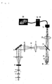
- [Figure 1] Figure 1 is an overall schematic diagram of the microscope device described in a first working configuration.
- Figure 1 shows an example of the construction of a microscope that modulates the phase of the illuminating light. In order from the light source, the illumination optical system is constructed from a
lamp light source 1, acollector lens 2, arelay lens 3, an opening diaphragm 4, afield lens 5, a diffraction grating 6, a condenser lens 7, areturn mirror 8 disposed in a pupil-conjugate position, arelay lens 9, avisual field diaphragm 10, a secondobjective lens 11, and a half-mirror 12. - The diffraction grating 6 is a diffraction grating having a one-dimensional transmissivity distribution in the direction perpendicular to the plane of the page; this diffraction grating generates diffracted light indicated by the broken line. In this technique, for reasons that will be described later, it is desirable that the diffraction grating have a narrow period in a range that allows projection of modulated illuminating light onto the sample in order to obtain a high spatial resolution.
- A phase diffraction grating having a light path difference of 1/2 wavelength with respect to the wavelength of the light source is desirable as the diffraction grating. However, it is sufficient if sufficiently narrow sinusoidal illumination can be performed on the sample; accordingly, for example, illumination with inclined light can be performed on a grating having a period in the vicinity of the image focusing limit, in which the transmissivity is modulated, or a light blocking plate can be disposed in a plane that is conjugate with the pupil of the objective lens so that only ± first-order light can pass through a diffraction grating having a period that allows focusing of the diffraction of ± first-order light as an image.
- The ± first-order light is separated by the diffraction grating 6 so that the respective light beams pass through the peripheral portions of the field lens 7, and the + first-order light and - first-order light form respective spots in positions on the peripheral portions of the return mirror. Here, the opening aperture 4 is adjusted so that there is no overlapping of the ± first-order light on the
return mirror 8. In cases where monochromatic light is utilized as the light source, there is no overlapping of the ± first-order light; in such a case, therefore, this opening aperture may be omitted. - The ± first-order light deflected by the
return mirror 8 passes through the edge portions of thepupil plane 14 of the objective lens, and the light beams interfere with each other in the vicinity of thesample 15, so that illumination is performed with illuminating light having a fringe structure. - Photography is performed by the
image pickup device 17. N images are acquired while the period is accurately shifted by 1/N in the direction perpendicular to the respective grating patterns by a diffraction grating driving device (not shown in the figures). However, N is 4 or greater, and is preferably as large as possible. - An image of the sample is formed by calculating the plurality of acquired images by the calculating means 19. The contents of the calculations will be shown next.
- In a microscope optical system having a point image intensity distribution Pr(x), when illumination having a certain intensity distribution is applied to the sample Or(x), the diffracted light in the sample is subjected to spatial modulation. In the case of sinusoidal illumination having a single spatial frequency component K, three modulated components, i.e., a zero-order component and ± first-order components, are obtained as spatially modulated components.
If this spatial modulation is expressed as
then the sample images subjected to spatial modulation can be expressed as follows:
Here, * indicates convolution integration. - Below, the quantity in real space is expressed by the attachment of a subscript r, and the quantity in fractional space is expressed by the attachment of a subscript k.
- If Equation (1) is subjected to a Fourier transform, and expressed in wave number space, we obtain the following:]

Here, the Fourier transform Pk(k) of Pr(x) expresses the transfer function of the optical system (OTF: optical transfer function). - Ok(k - K) and Ok(k + K) corresponding to 1 = -1 and 1 = 1 in Equation (2) mean that the spatial frequency component of the sample is shifted by the spatial frequency K of the illumination, so that even in the case of a microscope optical system in which only the spatial frequency component Pk(k) can be acquired, the high spatial frequency component of the sample can be acquired. Accordingly, it is desirable that the period of the illumination pattern be as short as possible in a range that allows focusing by this microscope optical system.
- When image pickup is performed while shifting the grating as described above, N images having the same modulation frequency and modulation amplitude, and having only a different modulation phase φ, are obtained. In this case, if the structured illumination phase of the jth image is expressed as φj, then the intensity Ikj(k) of the jth image signal is as follows:

Accordingly, N equations are obtained. - In these equations, Ok(k + 1K), (1 = -1, 0, 1) are unknowns; accordingly, these can be solved at N = 3, but if noise is contained in the picked-up images Ikj(k), the effect of this noise will cause the results obtained to be inaccurate. In cases where noise is thus contained in the observed quantities, as many images are picked up as possible, and it was discovered that the method of least squares is useful as a method for deriving values that are close to the true values from the unknowns.
- Accordingly, the most reasonable Ok(k + 1K) can be determined by applying the method of least squares to the N > 3 images described above.
- In concrete terms, setting blj = mlexp(iφj), Ok(k +1K)Pk(k) is determined by solving

- Since the signal is subjected to (as it were) averaging by the method of least squares processing described above, Ok(k +1K)Pk(k) in which the effect of noise superimposed on the original image is suppressed to a low value can be determined.
- Since Pk(k) is known, or can be measured beforehand, Ok(k + 1K) can be determined. Here, Ok(k + 1K) can also be determined simply by dividing Ok(k + 1K)Pk(k) by Pk(k); however, it is desirable to use a publicly known method that is not susceptible to the effects of noise, such as a Wiener filter.
- The detectable range of Pk(k) of a microscope optical system in a case where illumination that does not have an intensity distribution is applied is k = -2NA/λ to 2NA/λ with respect to the light wavelength λ and NA of the objective lens. Consequently, for 1= -1, 0, 1, Ok(k + 1K) obtained as described above contains the information of k = -2NA/λ - K to 2NA/λ - K, k = 2NA/λ to 2NA/λ, and k = -2NA/λ + K to 2NA/λ + K. Accordingly, Ok(k + 1K) overall contains information from k = -2NA/λ - K to 2NA/λ + K, so that microscopic images having a high resolution can be obtained by redefining this as Ok(k), performing a Fourier transform, and returning this to real space information Or(x).
- The images obtained as a result have a high resolution only in the one-dimensional direction in which spatial modulation is performed; however, a microscope which has a high two-dimensional resolution can be constructed by varying the direction in which spatial modulation is performed to at least two directions, and performing processing similar to the one-dimensional processing for these respective directions.
- Alternatively, a microscope having a high resolution in two directions can be constructed by constructing simultaneous equations by the method of least squares in two dimensions for spatially modulated images in at least two directions, and solving these equations.
- In concrete terms, for example, in cases where spatial modulation is performed in three directions, Okd(k + 1K)Pk(k) is an unknown for the three directions d = 1, 2, 3; accordingly, these may be determined. However, since the three zero-order diffraction components Ok1(k)Pk(k), Ok2(k)Pk(k) and Ok3(k)Pk(k) are in common here, there are seven simultaneous equations, and if the number of images in the respective modulation directions is Nd (d = 1, 2, 3), then we obtain the following:

The zero-order modulation component Ok(k)Pk(k) and the ± first-order components Okd(k ± K)Pk(k) for the three directions can be determined by solving these. - In this case, the problem is to determine seven unknowns by processing three or more images in structured illumination phases for spatial modulation in three directions. This is a state in which there is more data than unknowns.
- In such a case, Okd(k + 1K)Pk(k) cannot be uniquely determined without using the method of least squares. Accordingly, the method describe above is extremely effective in improving the two-dimensional resolution by varying the direction of one-dimensional modulation.
- Figure 1 shows an example of the construction of a microscope in which the phase of the illuminating light is modulated. In order from the light source, the illumination optical system is constructed from a lamp
light source 1, acollector lens 2, arelay lens 3, an opening diaphragm 4, a filedlens 5, adiffraction grating 6, a condenser lens 7, areturn mirror 8 disposed in a pupil-conjugate position, arelay lens 9, avisual field diaphragm 10, a secondobjective lens 11, and a half-mirror 12. - The
diffraction grating 6 is a diffraction grating having a sinusoidal transmissivity distribution proceeding directly in the plane perpendicular to the optical axis. It is sufficient if thediffraction grating 6 has diffraction patterns in two directions in the plane perpendicular to the optical axis. It is not absolutely necessary that these patterns be orthogonal; however, since the calculation processing in such a case is simple, it is desirable that the patterns be orthogonal. - This diffraction grating generates diffracted light indicated by a broken line by means of a grating in the direction perpendicular to the plane of the page. Furthermore, diffracted light (not shown in the figures) that passes vertically through the plane of the page is generated by a grating oriented in the plane of the page. In order to obtain a high spatial resolution by means of the present technique, it is desirable that the diffraction gratings have a narrow period in the range that allows the modulated illuminating light to be projected onto the sample. Accordingly, what must be taken into account in the diffracted light is only the ± first-order light. It is desirable that the periods of the gratings in the two directions be the same; however, in cases where there is no problem if the resolution is different in the two directions, the periods in the two directions may be different.
- It is necessary that the zero-order light components of the diffraction gratings be sufficiently small. Accordingly, phase diffraction gratings which are such that the light path difference is 1/2 wavelength with respect to the wavelength of the light source are desirable. However, it is sufficient if sufficiently narrow sinusoidal illumination can be performed with respect to the sample; accordingly, for example, illumination with inclined light can be performed on a grating having a period in the vicinity of the image focusing limit, in which the transmissivity is modulated, or a light blocking plate can be disposed in a plane that is conjugate with the pupil of the objective lens so that only ± first-order light can pass through a diffraction grating having a period that allows focusing of the diffraction of ± first-order light as an image.
- The ± first-order light is separated by the
diffraction grating 6 so that the respective light beams] pass through the peripheral portions of the field lens 7, and the + first-order light and - first-order light form respective spots in positions on the peripheral portions of the return mirror. Here, the opening aperture 4 is adjusted so that there is no overlapping of the ± first-order light on thereturn mirror 8. In cases where monochromatic light is utilized as the light source, there is no overlapping of the ± first-order light; in such a case, therefore, this opening aperture may be omitted. - The ± first-order light deflected by the
return mirror 8 passes through the edge portions of thepupil plane 14 of the objective lens, and the light beams] interfere with each other in the vicinity of thesample 15, so that illumination is performed with illuminating light having a fringe structure. - Photography is performed by the
image pickup device 17. Since the diffraction grating comprises gratings in two directly proceeding directions, the surface of the sample is illuminated with grating patterns in two directly proceeding directions. Images are acquired while the position is accurately shifted by 1/N of the period in the directions of the respective grating patterns by a diffraction grating driving device not shown in the figures. - Specifically, N images are first acquired while the position is shifted by 1/N at a time in the direction of one grating (this is taken as the Y direction). Next, the position is shifted by 1/N in the direction of the other grating (this is taken as the X direction), and N images are then acquired while the position is shifted by 1/N at a time in the Y direction. Subsequently, this is repeated, so that N2 images are acquired by shifting the position N times in the X direction as well.
- When image pickup is performed while shifting the grating as described above, N images of the same phase in one grating pattern can be acquired ; however, these images have a different modulation amplitude as a result of the other grating pattern. Specifically, where the x and y directions are the respective directions of the grating patterns described above, the structured illumination intensity Iri is generally written as follows:

Accordingly, if shifting is performed in the x direction so that φx = 0, ..., 2πj/N, ..., 2π(N - 1)/N, the illumination amplitude in the y direction at a specified x has a value that is proportional to cos(2πj/N). That is, images that have a different modulation amplitude are obtained. - An image of the sample is formed by calculation applied to the plurality of picked-up images by the calculation means 19. With regard to the calculation processing, the method described in the previous example may be applied by being expanded to two dimensions.
Claims (7)
- An image forming method in which a sample is illuminated with spatially modulated illuminating light,
light from the sample illuminated by the illuminating light is focused as an image, and a sample image is formed by image calculation processing from the acquired image, wherein
more images than the spatially modulated components of the illuminating light on the sample are acquired, and a sample image is formed by applying the method of least squares to the plurality of picked-up images. - The image forming method according to Claim 1, wherein the plurality of images are acquired while varying the phase of the illuminating light pattern on the sample.
- The image forming method according to Claim 1, wherein the plurality of images are acquired while varying the modulation amplitude of the illuminating light on the sample.
- A microscope device comprising:a light source;an illumination optical system which illuminates a sample with light from the light source;a diffraction grating which is disposed in a position that is optically conjugate with the sample in the illumination optical system;a modulation device which modulates the diffraction grating, and which illuminates the sample with spatially modulated light;an image pickup means which picks up spatially modulated sample images from the sample; andan image forming device which forms an image of the sample by applying the method of least squares to more images than the spatially modulated components of the illuminating light on the sample, which are picked up by the image pickup means.
- The microscope device according to Claim 4, wherein the image pickup means picks up a plurality of images in which the phase of the illuminating light pattern on the sample is varied.
- The microscope device according to Claim 4, wherein the image pickup means picks up a plurality of images in which the modulation amplitude of the illuminating light on the sample is varied.
- The microscope device according to Claim 4, wherein
the diffraction grating has grating patterns in two directions in the plane perpendicular to the optical axis, and
the modulation device moves the diffraction grating in the directions respectively perpendicular to these two directions.
Applications Claiming Priority (3)
| Application Number | Priority Date | Filing Date | Title |
|---|---|---|---|
| JP2005096920 | 2005-03-30 | ||
| JP2005293658 | 2005-10-06 | ||
| PCT/JP2006/305564 WO2006109448A1 (en) | 2005-03-30 | 2006-03-20 | Image forming method and microscope device |
Publications (3)
| Publication Number | Publication Date |
|---|---|
| EP1865355A1 true EP1865355A1 (en) | 2007-12-12 |
| EP1865355A4 EP1865355A4 (en) | 2009-06-24 |
| EP1865355B1 EP1865355B1 (en) | 2013-03-06 |
Family
ID=37086739
Family Applications (1)
| Application Number | Title | Priority Date | Filing Date |
|---|---|---|---|
| EP06729532A Expired - Lifetime EP1865355B1 (en) | 2005-03-30 | 2006-03-20 | Image forming method and microscope device |
Country Status (4)
| Country | Link |
|---|---|
| US (1) | US8115806B2 (en) |
| EP (1) | EP1865355B1 (en) |
| JP (1) | JP4123305B2 (en) |
| WO (1) | WO2006109448A1 (en) |
Cited By (1)
| Publication number | Priority date | Publication date | Assignee | Title |
|---|---|---|---|---|
| EP2806262A4 (en) * | 2012-01-18 | 2015-09-23 | Nikon Corp | STRUCTURED LIGHTING DEVICE, LIGHTED MICROSCOPE STRUCTURED DEVICE, AND STRUCTURED LIGHTING METHOD |
Families Citing this family (21)
| Publication number | Priority date | Publication date | Assignee | Title |
|---|---|---|---|---|
| FR2922658B1 (en) * | 2007-10-18 | 2011-02-04 | Centre Nat Rech Scient | STRUCTURED ILLUMINATION SYSTEM OF A SAMPLE |
| EP2610662B1 (en) * | 2010-08-25 | 2018-04-04 | Nikon Corporation | Microscope optical assembly and microscope system |
| JP5594429B2 (en) | 2011-05-06 | 2014-09-24 | 株式会社ニコン | Structured illumination microscope and structured illumination observation method |
| WO2013001805A1 (en) | 2011-06-29 | 2013-01-03 | 株式会社ニコン | Structured illumination optical system and structured illumination microscope device |
| WO2013011680A1 (en) | 2011-07-15 | 2013-01-24 | 株式会社ニコン | Structured illumination device, structured illumination microscope, and structured illumination method |
| JP5562919B2 (en) | 2011-09-30 | 2014-07-30 | オリンパス株式会社 | Super-resolution observation device |
| WO2013130681A1 (en) * | 2012-02-27 | 2013-09-06 | Integrated Medical Systems International, Inc. | Systems and methods for identifying optical material |
| WO2015008415A1 (en) | 2013-07-17 | 2015-01-22 | 株式会社ニコン | Structured illumination device and structured illumination microscope device |
| JP6351951B2 (en) * | 2013-10-22 | 2018-07-04 | 浜松ホトニクス株式会社 | Total reflection light irradiation device |
| EP3081976B1 (en) | 2013-12-12 | 2022-06-15 | Nikon Corporation | Structured illumination microscope, structured illumination method and program |
| JP6260691B2 (en) | 2014-04-25 | 2018-01-17 | 株式会社ニコン | Structured illumination microscope apparatus and structured illumination observation method |
| JP6635052B2 (en) * | 2015-02-05 | 2020-01-22 | 株式会社ニコン | Structured illumination microscope and observation method |
| WO2016151665A1 (en) * | 2015-03-20 | 2016-09-29 | 株式会社ニコン | Structured illumination microscope, observation method, and image processing program |
| US10989661B2 (en) * | 2015-05-01 | 2021-04-27 | The Board Of Regents Of The University Of Texas System | Uniform and scalable light-sheets generated by extended focusing |
| WO2016199179A1 (en) | 2015-06-08 | 2016-12-15 | 株式会社ニコン | Structured illumination microscope system, method, and program |
| JP6645506B2 (en) | 2015-10-19 | 2020-02-14 | 株式会社ニコン | Structured illumination microscope, observation method, and microscope control program |
| WO2017180680A1 (en) | 2016-04-12 | 2017-10-19 | The Board Of Regents Of The University Of Texas System | LIGHT-SHEET MICROSCOPE WITH PARALLELIZED 3D lMAGE ACQUISITION |
| US11378544B2 (en) | 2018-01-08 | 2022-07-05 | Illumina, Inc. | High-throughput sequencing with semiconductor-based detection |
| KR102370055B1 (en) | 2018-01-08 | 2022-03-03 | 일루미나, 인코포레이티드 | Systems and devices for high-throughput sequencing with semiconductor-based detection |
| NL2020621B1 (en) * | 2018-01-08 | 2019-07-15 | Illumina Inc | Multiplexing of an active sensor detector using structured illumination |
| JP7572033B2 (en) * | 2020-10-23 | 2024-10-23 | 株式会社リガク | Imaging X-ray microscope |
Family Cites Families (4)
| Publication number | Priority date | Publication date | Assignee | Title |
|---|---|---|---|---|
| JPH08149458A (en) | 1994-11-18 | 1996-06-07 | Sony Corp | Video processing device |
| US5943133A (en) * | 1996-12-04 | 1999-08-24 | The Research Foundation Of City College Of New York | System and method for performing selected optical measurements on a sample using a diffraction grating |
| JPH11242189A (en) * | 1997-12-25 | 1999-09-07 | Olympus Optical Co Ltd | Image forming method, image forming apparatus |
| JP4729812B2 (en) * | 2001-06-27 | 2011-07-20 | ソニー株式会社 | Image processing apparatus and method, recording medium, and program |
-
2006
- 2006-03-20 EP EP06729532A patent/EP1865355B1/en not_active Expired - Lifetime
- 2006-03-20 US US11/886,847 patent/US8115806B2/en active Active
- 2006-03-20 WO PCT/JP2006/305564 patent/WO2006109448A1/en not_active Ceased
- 2006-03-20 JP JP2007512446A patent/JP4123305B2/en not_active Expired - Lifetime
Cited By (2)
| Publication number | Priority date | Publication date | Assignee | Title |
|---|---|---|---|---|
| EP2806262A4 (en) * | 2012-01-18 | 2015-09-23 | Nikon Corp | STRUCTURED LIGHTING DEVICE, LIGHTED MICROSCOPE STRUCTURED DEVICE, AND STRUCTURED LIGHTING METHOD |
| US10802259B2 (en) | 2012-01-18 | 2020-10-13 | Nikon Corporation | Structured illuminating apparatus, structured illuminating microscopy apparatus, and structured illuminating method |
Also Published As
| Publication number | Publication date |
|---|---|
| EP1865355B1 (en) | 2013-03-06 |
| JPWO2006109448A1 (en) | 2008-10-16 |
| JP4123305B2 (en) | 2008-07-23 |
| US8115806B2 (en) | 2012-02-14 |
| EP1865355A4 (en) | 2009-06-24 |
| WO2006109448A1 (en) | 2006-10-19 |
| US20100141750A1 (en) | 2010-06-10 |
Similar Documents
| Publication | Publication Date | Title |
|---|---|---|
| EP1865355B1 (en) | Image forming method and microscope device | |
| US8081378B2 (en) | Microscope | |
| US6239909B1 (en) | Image-forming method and image-forming apparatus | |
| US10712270B2 (en) | Digital holographic microscope | |
| EP3081976B1 (en) | Structured illumination microscope, structured illumination method and program | |
| EP2437095B1 (en) | Sample observation device for generating super resolution image | |
| JP5357329B2 (en) | Observation device | |
| EP2329324B1 (en) | Method to investigate nano-sized objects using holographic microscopy | |
| US10754139B2 (en) | Three-dimensional position information acquiring method and three-dimensional position information acquiring apparatus | |
| JP2009098215A (en) | Microscope device and method for calculating phase change amount in microscope device. | |
| US7002695B2 (en) | Dual-spot phase-sensitive detection | |
| US20250013026A1 (en) | Multi-focal light-sheet structured illumination fluorescence microscopy system | |
| JP4978470B2 (en) | Microscope apparatus and observation method | |
| JP7090334B2 (en) | Optical distance measuring device | |
| Cogswell et al. | High-resolution confocal transmission microscope, Part I: system design | |
| WO2003034010A1 (en) | Phase determination of a radiation wavefield | |
| CN114137713A (en) | Real-time quantitative phase imaging method and system for unmarked thick sample | |
| EP3901684A1 (en) | Optical fluorescence microscope and method for the obtaining of optical fluorescence microscopy images | |
| JPH05188327A (en) | Differential phase image observation device | |
| JP2022118395A (en) | Optical measuring device and data operation method of optical measuring device | |
| Ishiwata et al. | Quantitative phase analysis in retardation-modulated differential interference contrast (RM-DIC) microscope | |
| Young | Holography and Image Processing |
Legal Events
| Date | Code | Title | Description |
|---|---|---|---|
| PUAI | Public reference made under article 153(3) epc to a published international application that has entered the european phase |
Free format text: ORIGINAL CODE: 0009012 |
|
| 17P | Request for examination filed |
Effective date: 20070910 |
|
| AK | Designated contracting states |
Kind code of ref document: A1 Designated state(s): AT BE BG CH CY CZ DE DK EE ES FI FR GB GR HU IE IS IT LI LT LU LV MC NL PL PT RO SE SI SK TR |
|
| DAX | Request for extension of the european patent (deleted) | ||
| A4 | Supplementary search report drawn up and despatched |
Effective date: 20090528 |
|
| 17Q | First examination report despatched |
Effective date: 20090902 |
|
| RAP1 | Party data changed (applicant data changed or rights of an application transferred) |
Owner name: NIKON CORPORATION |
|
| GRAP | Despatch of communication of intention to grant a patent |
Free format text: ORIGINAL CODE: EPIDOSNIGR1 |
|
| GRAP | Despatch of communication of intention to grant a patent |
Free format text: ORIGINAL CODE: EPIDOSNIGR1 |
|
| GRAS | Grant fee paid |
Free format text: ORIGINAL CODE: EPIDOSNIGR3 |
|
| GRAA | (expected) grant |
Free format text: ORIGINAL CODE: 0009210 |
|
| AK | Designated contracting states |
Kind code of ref document: B1 Designated state(s): AT BE BG CH CY CZ DE DK EE ES FI FR GB GR HU IE IS IT LI LT LU LV MC NL PL PT RO SE SI SK TR |
|
| REG | Reference to a national code |
Ref country code: GB Ref legal event code: FG4D |
|
| REG | Reference to a national code |
Ref country code: AT Ref legal event code: REF Ref document number: 599953 Country of ref document: AT Kind code of ref document: T Effective date: 20130315 Ref country code: CH Ref legal event code: EP |
|
| REG | Reference to a national code |
Ref country code: IE Ref legal event code: FG4D |
|
| REG | Reference to a national code |
Ref country code: DE Ref legal event code: R096 Ref document number: 602006034903 Country of ref document: DE Effective date: 20130502 |
|
| REG | Reference to a national code |
Ref country code: AT Ref legal event code: MK05 Ref document number: 599953 Country of ref document: AT Kind code of ref document: T Effective date: 20130306 |
|
| PG25 | Lapsed in a contracting state [announced via postgrant information from national office to epo] |
Ref country code: ES Free format text: LAPSE BECAUSE OF FAILURE TO SUBMIT A TRANSLATION OF THE DESCRIPTION OR TO PAY THE FEE WITHIN THE PRESCRIBED TIME-LIMIT Effective date: 20130617 Ref country code: BG Free format text: LAPSE BECAUSE OF FAILURE TO SUBMIT A TRANSLATION OF THE DESCRIPTION OR TO PAY THE FEE WITHIN THE PRESCRIBED TIME-LIMIT Effective date: 20130606 Ref country code: AT Free format text: LAPSE BECAUSE OF FAILURE TO SUBMIT A TRANSLATION OF THE DESCRIPTION OR TO PAY THE FEE WITHIN THE PRESCRIBED TIME-LIMIT Effective date: 20130306 Ref country code: SE Free format text: LAPSE BECAUSE OF FAILURE TO SUBMIT A TRANSLATION OF THE DESCRIPTION OR TO PAY THE FEE WITHIN THE PRESCRIBED TIME-LIMIT Effective date: 20130306 Ref country code: LT Free format text: LAPSE BECAUSE OF FAILURE TO SUBMIT A TRANSLATION OF THE DESCRIPTION OR TO PAY THE FEE WITHIN THE PRESCRIBED TIME-LIMIT Effective date: 20130306 |
|
| REG | Reference to a national code |
Ref country code: NL Ref legal event code: VDEP Effective date: 20130306 |
|
| REG | Reference to a national code |
Ref country code: LT Ref legal event code: MG4D |
|
| PG25 | Lapsed in a contracting state [announced via postgrant information from national office to epo] |
Ref country code: GR Free format text: LAPSE BECAUSE OF FAILURE TO SUBMIT A TRANSLATION OF THE DESCRIPTION OR TO PAY THE FEE WITHIN THE PRESCRIBED TIME-LIMIT Effective date: 20130607 Ref country code: LV Free format text: LAPSE BECAUSE OF FAILURE TO SUBMIT A TRANSLATION OF THE DESCRIPTION OR TO PAY THE FEE WITHIN THE PRESCRIBED TIME-LIMIT Effective date: 20130306 Ref country code: FI Free format text: LAPSE BECAUSE OF FAILURE TO SUBMIT A TRANSLATION OF THE DESCRIPTION OR TO PAY THE FEE WITHIN THE PRESCRIBED TIME-LIMIT Effective date: 20130306 Ref country code: SI Free format text: LAPSE BECAUSE OF FAILURE TO SUBMIT A TRANSLATION OF THE DESCRIPTION OR TO PAY THE FEE WITHIN THE PRESCRIBED TIME-LIMIT Effective date: 20130306 |
|
| PG25 | Lapsed in a contracting state [announced via postgrant information from national office to epo] |
Ref country code: BE Free format text: LAPSE BECAUSE OF FAILURE TO SUBMIT A TRANSLATION OF THE DESCRIPTION OR TO PAY THE FEE WITHIN THE PRESCRIBED TIME-LIMIT Effective date: 20130306 |
|
| PG25 | Lapsed in a contracting state [announced via postgrant information from national office to epo] |
Ref country code: RO Free format text: LAPSE BECAUSE OF FAILURE TO SUBMIT A TRANSLATION OF THE DESCRIPTION OR TO PAY THE FEE WITHIN THE PRESCRIBED TIME-LIMIT Effective date: 20130306 Ref country code: PT Free format text: LAPSE BECAUSE OF FAILURE TO SUBMIT A TRANSLATION OF THE DESCRIPTION OR TO PAY THE FEE WITHIN THE PRESCRIBED TIME-LIMIT Effective date: 20130708 Ref country code: EE Free format text: LAPSE BECAUSE OF FAILURE TO SUBMIT A TRANSLATION OF THE DESCRIPTION OR TO PAY THE FEE WITHIN THE PRESCRIBED TIME-LIMIT Effective date: 20130306 Ref country code: CZ Free format text: LAPSE BECAUSE OF FAILURE TO SUBMIT A TRANSLATION OF THE DESCRIPTION OR TO PAY THE FEE WITHIN THE PRESCRIBED TIME-LIMIT Effective date: 20130306 Ref country code: IS Free format text: LAPSE BECAUSE OF FAILURE TO SUBMIT A TRANSLATION OF THE DESCRIPTION OR TO PAY THE FEE WITHIN THE PRESCRIBED TIME-LIMIT Effective date: 20130706 Ref country code: NL Free format text: LAPSE BECAUSE OF FAILURE TO SUBMIT A TRANSLATION OF THE DESCRIPTION OR TO PAY THE FEE WITHIN THE PRESCRIBED TIME-LIMIT Effective date: 20130306 Ref country code: SK Free format text: LAPSE BECAUSE OF FAILURE TO SUBMIT A TRANSLATION OF THE DESCRIPTION OR TO PAY THE FEE WITHIN THE PRESCRIBED TIME-LIMIT Effective date: 20130306 Ref country code: MC Free format text: LAPSE BECAUSE OF NON-PAYMENT OF DUE FEES Effective date: 20130331 |
|
| REG | Reference to a national code |
Ref country code: CH Ref legal event code: PL |
|
| PG25 | Lapsed in a contracting state [announced via postgrant information from national office to epo] |
Ref country code: CY Free format text: LAPSE BECAUSE OF FAILURE TO SUBMIT A TRANSLATION OF THE DESCRIPTION OR TO PAY THE FEE WITHIN THE PRESCRIBED TIME-LIMIT Effective date: 20130306 Ref country code: PL Free format text: LAPSE BECAUSE OF FAILURE TO SUBMIT A TRANSLATION OF THE DESCRIPTION OR TO PAY THE FEE WITHIN THE PRESCRIBED TIME-LIMIT Effective date: 20130306 |
|
| REG | Reference to a national code |
Ref country code: IE Ref legal event code: MM4A |
|
| PLBE | No opposition filed within time limit |
Free format text: ORIGINAL CODE: 0009261 |
|
| STAA | Information on the status of an ep patent application or granted ep patent |
Free format text: STATUS: NO OPPOSITION FILED WITHIN TIME LIMIT |
|
| PG25 | Lapsed in a contracting state [announced via postgrant information from national office to epo] |
Ref country code: IE Free format text: LAPSE BECAUSE OF NON-PAYMENT OF DUE FEES Effective date: 20130320 Ref country code: LI Free format text: LAPSE BECAUSE OF NON-PAYMENT OF DUE FEES Effective date: 20130331 Ref country code: DK Free format text: LAPSE BECAUSE OF FAILURE TO SUBMIT A TRANSLATION OF THE DESCRIPTION OR TO PAY THE FEE WITHIN THE PRESCRIBED TIME-LIMIT Effective date: 20130306 Ref country code: CH Free format text: LAPSE BECAUSE OF NON-PAYMENT OF DUE FEES Effective date: 20130331 |
|
| 26N | No opposition filed |
Effective date: 20131209 |
|
| GBPC | Gb: european patent ceased through non-payment of renewal fee |
Effective date: 20130606 |
|
| PG25 | Lapsed in a contracting state [announced via postgrant information from national office to epo] |
Ref country code: IT Free format text: LAPSE BECAUSE OF FAILURE TO SUBMIT A TRANSLATION OF THE DESCRIPTION OR TO PAY THE FEE WITHIN THE PRESCRIBED TIME-LIMIT Effective date: 20130306 |
|
| REG | Reference to a national code |
Ref country code: DE Ref legal event code: R097 Ref document number: 602006034903 Country of ref document: DE Effective date: 20131209 |
|
| PG25 | Lapsed in a contracting state [announced via postgrant information from national office to epo] |
Ref country code: GB Free format text: LAPSE BECAUSE OF NON-PAYMENT OF DUE FEES Effective date: 20130606 |
|
| PG25 | Lapsed in a contracting state [announced via postgrant information from national office to epo] |
Ref country code: TR Free format text: LAPSE BECAUSE OF FAILURE TO SUBMIT A TRANSLATION OF THE DESCRIPTION OR TO PAY THE FEE WITHIN THE PRESCRIBED TIME-LIMIT Effective date: 20130306 |
|
| PG25 | Lapsed in a contracting state [announced via postgrant information from national office to epo] |
Ref country code: LU Free format text: LAPSE BECAUSE OF NON-PAYMENT OF DUE FEES Effective date: 20130320 Ref country code: HU Free format text: LAPSE BECAUSE OF FAILURE TO SUBMIT A TRANSLATION OF THE DESCRIPTION OR TO PAY THE FEE WITHIN THE PRESCRIBED TIME-LIMIT; INVALID AB INITIO Effective date: 20060320 |
|
| PG25 | Lapsed in a contracting state [announced via postgrant information from national office to epo] |
Ref country code: FR Free format text: LAPSE BECAUSE OF NON-PAYMENT OF DUE FEES Effective date: 20130331 |
|
| P01 | Opt-out of the competence of the unified patent court (upc) registered |
Effective date: 20230517 |
|
| PGFP | Annual fee paid to national office [announced via postgrant information from national office to epo] |
Ref country code: DE Payment date: 20250128 Year of fee payment: 20 |
|
| REG | Reference to a national code |
Ref country code: DE Ref legal event code: R071 Ref document number: 602006034903 Country of ref document: DE |