EP1863176A1 - Procédé et appareil pour joint torique à diode active intégrée et commutation électrique souple - Google Patents
Procédé et appareil pour joint torique à diode active intégrée et commutation électrique souple Download PDFInfo
- Publication number
- EP1863176A1 EP1863176A1 EP07108000A EP07108000A EP1863176A1 EP 1863176 A1 EP1863176 A1 EP 1863176A1 EP 07108000 A EP07108000 A EP 07108000A EP 07108000 A EP07108000 A EP 07108000A EP 1863176 A1 EP1863176 A1 EP 1863176A1
- Authority
- EP
- European Patent Office
- Prior art keywords
- power supply
- switch module
- module
- input
- parameter relating
- Prior art date
- Legal status (The legal status is an assumption and is not a legal conclusion. Google has not performed a legal analysis and makes no representation as to the accuracy of the status listed.)
- Withdrawn
Links
Images


Classifications
-
- H—ELECTRICITY
- H02—GENERATION; CONVERSION OR DISTRIBUTION OF ELECTRIC POWER
- H02J—CIRCUIT ARRANGEMENTS OR SYSTEMS FOR SUPPLYING OR DISTRIBUTING ELECTRIC POWER; SYSTEMS FOR STORING ELECTRIC ENERGY
- H02J1/00—Circuit arrangements for dc mains or dc distribution networks
- H02J1/10—Parallel operation of dc sources
-
- H—ELECTRICITY
- H02—GENERATION; CONVERSION OR DISTRIBUTION OF ELECTRIC POWER
- H02J—CIRCUIT ARRANGEMENTS OR SYSTEMS FOR SUPPLYING OR DISTRIBUTING ELECTRIC POWER; SYSTEMS FOR STORING ELECTRIC ENERGY
- H02J1/00—Circuit arrangements for dc mains or dc distribution networks
- H02J1/001—Hot plugging or unplugging of load or power modules to or from power distribution networks
-
- H—ELECTRICITY
- H03—ELECTRONIC CIRCUITRY
- H03K—PULSE TECHNIQUE
- H03K17/00—Electronic switching or gating, i.e. not by contact-making and –breaking
- H03K17/16—Modifications for eliminating interference voltages or currents
- H03K17/161—Modifications for eliminating interference voltages or currents in field-effect transistor switches
-
- H—ELECTRICITY
- H03—ELECTRONIC CIRCUITRY
- H03K—PULSE TECHNIQUE
- H03K17/00—Electronic switching or gating, i.e. not by contact-making and –breaking
- H03K17/30—Modifications for providing a predetermined threshold before switching
- H03K17/302—Modifications for providing a predetermined threshold before switching in field-effect transistor switches
-
- H—ELECTRICITY
- H03—ELECTRONIC CIRCUITRY
- H03K—PULSE TECHNIQUE
- H03K17/00—Electronic switching or gating, i.e. not by contact-making and –breaking
- H03K17/51—Electronic switching or gating, i.e. not by contact-making and –breaking characterised by the components used
- H03K17/56—Electronic switching or gating, i.e. not by contact-making and –breaking characterised by the components used by the use, as active elements, of semiconductor devices
- H03K17/687—Electronic switching or gating, i.e. not by contact-making and –breaking characterised by the components used by the use, as active elements, of semiconductor devices the devices being field-effect transistors
- H03K17/6871—Electronic switching or gating, i.e. not by contact-making and –breaking characterised by the components used by the use, as active elements, of semiconductor devices the devices being field-effect transistors the output circuit comprising more than one controlled field-effect transistor
- H03K17/6872—Electronic switching or gating, i.e. not by contact-making and –breaking characterised by the components used by the use, as active elements, of semiconductor devices the devices being field-effect transistors the output circuit comprising more than one controlled field-effect transistor using complementary field-effect transistors
-
- H—ELECTRICITY
- H03—ELECTRONIC CIRCUITRY
- H03K—PULSE TECHNIQUE
- H03K17/00—Electronic switching or gating, i.e. not by contact-making and –breaking
- H03K17/51—Electronic switching or gating, i.e. not by contact-making and –breaking characterised by the components used
- H03K17/56—Electronic switching or gating, i.e. not by contact-making and –breaking characterised by the components used by the use, as active elements, of semiconductor devices
- H03K17/687—Electronic switching or gating, i.e. not by contact-making and –breaking characterised by the components used by the use, as active elements, of semiconductor devices the devices being field-effect transistors
- H03K17/6877—Electronic switching or gating, i.e. not by contact-making and –breaking characterised by the components used by the use, as active elements, of semiconductor devices the devices being field-effect transistors the control circuit comprising active elements different from those used in the output circuit
-
- H—ELECTRICITY
- H02—GENERATION; CONVERSION OR DISTRIBUTION OF ELECTRIC POWER
- H02J—CIRCUIT ARRANGEMENTS OR SYSTEMS FOR SUPPLYING OR DISTRIBUTING ELECTRIC POWER; SYSTEMS FOR STORING ELECTRIC ENERGY
- H02J2310/00—The network for supplying or distributing electric power characterised by its spatial reach or by the load
- H02J2310/40—The network being an on-board power network, i.e. within a vehicle
-
- Y—GENERAL TAGGING OF NEW TECHNOLOGICAL DEVELOPMENTS; GENERAL TAGGING OF CROSS-SECTIONAL TECHNOLOGIES SPANNING OVER SEVERAL SECTIONS OF THE IPC; TECHNICAL SUBJECTS COVERED BY FORMER USPC CROSS-REFERENCE ART COLLECTIONS [XRACs] AND DIGESTS
- Y02—TECHNOLOGIES OR APPLICATIONS FOR MITIGATION OR ADAPTATION AGAINST CLIMATE CHANGE
- Y02T—CLIMATE CHANGE MITIGATION TECHNOLOGIES RELATED TO TRANSPORTATION
- Y02T50/00—Aeronautics or air transport
- Y02T50/50—On board measures aiming to increase energy efficiency
Definitions
- the present invention relates to electric power systems, and more particularly to a method and apparatus for connection of multiple power supply inputs, and for soft-switching during hot swap of modules for AC and DC electric power systems.
- Electric systems used in complex environments such as aerospace systems, more electric aircraft systems, industrial environments, vehicles, etc., include a large number of electric modules.
- Various electric modules may need to be extracted and replaced with other modules, to change functionality or to replace modules that exhibit faults.
- Hot swap, hot-plug, and hot-dock are terms used interchangeably to refer to the process of safely inserting or removing cards, PC boards, cables, and/or modules from a host system without removing power.
- the goal of hot swap is to insert or remove modules without disturbing, damaging, or degrading up/down-stream adjacent line replaceable modules/ subsystems, to increase system availability, reduce down time, simplify system repair, and allow for system maintenance/upgrade without interrupting service to other loads.
- Electric modules included in environments such as aerospace systems, more electric aircraft systems, industrial environments, vehicles, etc. may be connected to multiple power supply voltage inputs, and extract one voltage output to be used by the modules.
- the multiple power supply voltage inputs are also connected or disconnected from the host system, or from the removable electrical modules, without removing power.
- hot swap can cause severe electrical, mechanical, thermal and operational problems in an electrical system.
- pulling a board/module out while there is current passing through the module connectors, or inserting a board/module with all bulk/bypass capacitors at zero volts can introduce severe electrical voltage/ current transients which may adversely impact reliability and lead to safety consequences.
- Current chopping introduces Ldi / dt variations (where L is inductance of a load, for example) leading to very large voltage transients which are a major safety concern for maintenance people, as large voltage transients can cause high voltage electrical shock.
- Typical/ conventional methods use passive diode-ORing systems to connect multiple power supply voltage inputs to a supply bus for replaceable modules. Such passive diode-ORing systems result in excessive power losses and voltage drops. Significant voltage drops, particularly when preferred paths of power consumption from AC and DC sources are required, are a major problem. Current chopping occurring during insertion or extraction of modules is a major contributor to excessive voltage/current transients that stress and damage individual components and reduce the Mean Time Between Failure (MTBF) for the host system and for the removable modules.
- MTBF Mean Time Between Failure
- a disclosed embodiment of the application addresses these and other issues by utilizing a method and apparatus for integrated active-diode-ORing and soft power switching.
- the method and apparatus achieve proper connection of multiple power supply voltage inputs to realize a fault tolerant power supply bus for replaceable modules.
- the method and apparatus provide soft power-up/down capability during hot swap of modules for AC and DC electric power systems.
- the method and apparatus provide a single power bus from multiple power supply inputs, with minimum voltage drop, improved efficiency, and no looses in passive diodes.
- the method and apparatus provide integrated soft-switching that reduces turn-on in-rush current during board/module insertion and further eliminates current-chopping during interruption of current in inductive circuits.
- the method and apparatus can be used for both low and high power systems.
- an apparatus for power supply input connection comprises: a first switch module connected to a first power supply input; a first controller module connected to the first power supply input and to a secondary power connection, wherein said first controller module puts the first switch module in a first operating state when a parameter relating to the first power supply input is larger than a parameter relating to the secondary power connection, and puts the first switch module in a second operating state when the parameter relating to the first power supply input is smaller than the parameter relating to the secondary power connection; and a first driver module connected to the first controller module and to the first switch module, wherein the first driver module modifies a parameter relating to a drive characteristic of the first switch module.
- an apparatus for power supply input connection comprises: a first switch module connected to a first power supply input, the first switch module including a first field effect transistor; a first controller module connected to the first power supply input and to a secondary power connection, wherein the first controller module puts the first switch module in a first operating state when a parameter relating to the first power supply input is larger than a parameter relating to the secondary power connection, and puts the first switch module in a second operating state when the parameter relating to the first power supply input is smaller than the parameter relating to the secondary power connection; a first driver module connected to the first controller module and to the first switch module, wherein the first driver module modifies a parameter relating to a drive characteristic of the first switch module; and a first resistor connected to a body diode of the first field effect transistor, wherein the first resistor and the body diode of the first field effect transistor are connected in series between the first power supply input and the secondary power connection.
- a method for connection of power supply inputs comprises: providing a first power supply voltage input, a second power supply voltage input, and an output; isolating the first power supply voltage input from the output with a first switch module, the first switch module including a first gate; isolating the second power supply voltage input from the output with a second switch module, the second switch module including a second gate; and controlling the first switch module and the second switch module, the controlling step including turning the first switch module on when a voltage of the first power supply voltage input is larger than a voltage of the second power supply voltage input, turning the first switch module off when the voltage of the first power supply voltage input is smaller than the voltage of the second power supply voltage input, turning the second switch module on when a voltage of the second power supply voltage input is larger than a voltage of the first power supply voltage input, turning the second switch module off when the voltage of the second power supply voltage input is smaller than the voltage of the first power supply voltage input, modifying a parameter relating to a gate drive characteristic of the
- FIG. 1 is a general block diagram of an electrical system including a system for active-diode-ORing and soft power switching according to an embodiment of the present invention
- FIG. 2 is a block diagram of an electrical configuration containing a system for active-diode-ORing and soft power switching according to an embodiment of the present invention illustrated in FIG. 1;
- FIG. 3A is a typical/ conventional block diagram showing an electrical configuration containing a diode ORing system consisting of schottky diodes;
- FIG. 3B is a typical/ conventional block diagram showing an electrical configuration containing an active ORing circuit with one FET without driver;
- FIG. 3C is a graph for load transfer between input sources for the electrical configuration containing an active ORing circuit with one FET without driver illustrated in FIG. 3B;
- FIG. 4A is a block diagram of an electrical configuration containing an active ORing circuit with one FET with a driver according to an embodiment of the present invention
- FIG. 4B is a graph for load transfer between input sources for the electrical configuration containing an active ORing circuit with one FET with a driver according to an embodiment of the present invention illustrated in FIG. 4A;
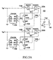
- FIG. 5A is a block diagram of an electrical configuration containing an active ORing circuit with two FETs with a driver according to a second embodiment of the present invention
- FIGS. 5B and 5C are graphs for signals and load transfers between input sources for the electrical configuration containing an active ORing circuit with two FETs with a driver according to a second embodiment of the present invention illustrated in FIG. 5A;
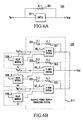
- FIG. 6A is a typical/ conventional general block diagram illustrating a circuit for soft-start of a source and load
- FIG. 6B is a block diagram of an electrical system incorporating soft start/stop into a multiple input/output power supply system using an active ORing circuit according to a third embodiment of the present invention.
- FIG. 7 illustrates an exemplary implementation for a block diagram of an electrical system incorporating soft start/stop into a multiple input/output power supply system using an active ORing circuit according to a third embodiment of the present invention illustrated in FIG. 6B;
- FIG. 8 illustrates another exemplary implementation for a block diagram of an electrical system incorporating soft start/stop into a multiple input/output power supply system using an active ORing circuit according to a third embodiment of the present invention illustrated in FIG. 6B;
- FIG. 9A is a graph of electrical parameters obtained when an LRM including the combined active ORing and soft-start circuit illustrated in FIG. 8 is plugged into a live PSM output;
- FIG. 9B is a graph of electrical parameters obtained when an LRM without an active ORing and soft-start circuit is plugged into a live PSM output;
- FIG. 9C is a graph of electrical parameters obtained when an LRM without an active ORing and soft-start circuit is unplugged from a live PSM.
- FIG. 9D is a graph of electrical parameters obtained when an LRM including the combined active ORing and soft-start circuit illustrated in FIG. 8 is unplugged from a live PSM output.
- FIG. 1 is a general block diagram of an electrical system including a system for active-diode-ORing and soft power switching according to an embodiment of the present invention.
- the electrical system 100 illustrated in FIG. I includes the following components: power source modules/ backplane 50_1, 50_2, 50_3; a multiple power supply connecting system 89; and electrical systems 60. Operation of the electrical system 100 in FIG. 1 will become apparent from the following discussion.
- Electrical system 100 may be associated with an aircraft, a more electric aircraft, a ship, a laboratory facility, an industrial environment, etc.
- the power source modules/ backplane 50_1, 50_2, 50_3 provide electrical energy in electrical system 100.
- the power source modules/ backplane 50_1, 50_2, 50_3 may include AC and DC power supplies, electrical components such as transformers, inductances, resistances, etc.
- the power source modules/ backplane 50_1, 50_2, 50_3 may provide high DC or AC voltages or low DC or AC voltages to electrical systems 60 through multiple power supply connecting system 89.
- Power inputs Vin1, Vin2, and Vin3 from power source modules/ backplane 50_1, 50_2, 50_3 are combined and integrated in multiple power supply connecting system 89, which outputs one voltage output Vout to electrical systems 60.
- Multiple power supply connecting system 89 includes three ORing systems 90_1, 90_2 and 90_3.
- ORing systems 90_1, 90_2 and 90_3 are integrated active-diode-OR circuits and realize a fault tolerant power supply bus for the electrical systems 60.
- Electrical systems 60 may include various electrical systems, such as systems on an aircraft or ship, navigation systems, cabin systems, air conditioning systems, etc., systems in an industrial facility such as electrical equipment and tools, etc.
- Electrical systems 60 may include DC and AC loads, which are electric circuits using DC and AC power that enable functioning of various services onboard a vehicle or aircraft, in a complex environment such as a laboratory facility, etc.
- Services using AC and DC power may be an electric motor, an automatic braking system, a lighting system of a vehicle, a piece of industrial equipment, etc.
- Electrical systems 60 may be replaceable modules that can be disconnected from electrical system 100, or inserted into electrical system 100. ORing systems 90_1, 90_2 and 90_3 provide soft power-up/down capability for electrical systems 60 during hot swap of electrical systems 60.
- ORing systems 90_1, 90_2 and 90_3 and electrical systems 60 may together be included in a replaceable module, so that ORing systems 90_1. 90_2 and 90_3 together with electrical systems 60 can be removed from or inserted into electrical system 100.
- ORing systems 90_1, 90_2 and 90_3 provide soft power-up/down capability for a replaceable module that includes electrical systems 60 and ORing systems 90_ 1, 90_2 and 90_3, during hot swap of the replaceable module from or into electrical system 100.
- Electrical systems 60 may be circuits/ devices included in replaceable module such as an AC or DC Line Replaceable Module (LRM), a card, a PC board, etc. Electrical systems 60 may be part of a high voltage AC or DC LRM. Electrical systems 60 may be included in a replaceable module with on-board Solid State Switching Devices (SSSDs). Electrical systems 60 may be included in a high voltage Solid State AC or DC replaceable module switch, referred to in the industry as a Solid State Remote Power Controller (SSPC).
- SSPC Solid State Remote Power Controller
- LRM Light-State-Ren-sote-Controller
- AC-SSPC-LRM AC Solid-State-Ren-sote-Controller
- DC-SSPC-LRM DC Solid-State-Remote-Controller
- Solid State AC and DC switches can be used with a wide range of powers, from a few Watts to hundreds of K Watts.
- LRMs including AC and DC Solid State Switching Devices (SSSDs) may manage high voltage AC and DC powers and loads, and may control the flow of electrical power to internal and external circuitry/loads, to achieve proper protection based on i 2 ⁇ t (instantaneous overcorrect protection for large currents and proportionally time-delayed overload protection for smaller currents) to protect the SSSDs or the wiring system.
- SSSDs Solid State Switching Devices
- Power source modules/ backplane 50_1, 50_2, 50_3 may provide various voltages to electrical systems 60 included in an LRM.
- Such voltages may be various AC voltages such as, for example, 115V or 230V or higher, with fixed frequencies (such as, for example, 50/60 Hz or 400Hz), or variable frequencies (such as, for example 360-800Hz for aerospace applications), or DC voltages such as, for example, 28V or 270V.
- the power of AC and DC LRMs may depend on the number of channels, as well as current rating and voltage of each channel. For example, an AC LRM for the Airbus A380 aircraft has 8 channels.
- AC and DC LRM boards are currently being deployed in aerospace and industry, and are poised to eventually replace traditional electromechanical AC/DC circuit breakers or relays, to reduce the overall system cost and weight, and improve reliability. Emerging Solid State AC and DC switches are poised to have widespread use in both commercial and military aerospace applications and general industry, for a few Watts to hundreds of KW power applications.
- AC and DC SSPC LRM cards do not include integrated active diode ORing circuits for soft power-up/down capability, and circuit breakers or relays which could be turned-off before initiating a hot swap of a failed LRM with one or more SSPC devices failed short. Hence, conventional hot swap is not properly designed for such LRM/ boards.
- ORing systems 90_1, 90_2 and 90_3 provide soft power-up/down capability for electrical systems 60 during hot swap of electrical systems 60, and protect components of electrical system 100 during hot swap insertion or removal of electrical systems 60 under normal or faulty modes of operation for high voltage DC and AC systems without the need to disconnect power.
- ORing systems 90_1, 90_2 and 90_3 are circuits with a combined function of active OR (low forward voltage drop and low reverse leakage) and soft-start/stop; provide integrated soft-switching to reduce turn-on in-rush current during board insertion; eliminate current-chopping during interruption of current in inductive circuits; contribute to safe and reliable insertion and removal of different types of LRMs during hot swap, without disturbing, damaging, or degrading up/down-stream adjacent LRMs and subsystems of electrical system 100; help high voltage AC and DC load management LRMs to control the flow of electrical power to internal and external circuitry/loads and achieve proper protection of SSSDs or the wiring system; provide a single power bus from multiple power supply input with minimized voltage drop and improved efficiency; help to safely insert a board/module when the board is not electrically initialized, and to safely pull a board-out while there is current passing through connectors; help provide hot swap protection beyond local boundaries of the replaceable modules; help mitigate hot swap effects, so that various bus activities and other operations taking place
- FIG. 1 Although three power supply voltage inputs are shown in FIG. 1, more than three or less than three power supply voltage inputs can be connected through multiple power supply connecting system 89, with each power supply voltage inputs connecting to its own ORing system inside multiple power supply connecting system 89.
- FIG. 2 is a block diagram of an electrical configuration containing a system for active-diode-ORing and soft power switching according to an embodiment of the present invention illustrated in FIG. 1.
- the electrical system illustrated in FIG. 2 includes two ORing systems 90_1 and 90_2.
- ORing system 90_1 includes a controller module 145_1, a switch module 143_1, and a driver module 160_1.
- ORing system 90_2 includes a controller module 145_2, a switch module 143_2, and a driver module 160_2.
- Controller module 145_1 is connected to a first power supply input Vin1, and controller module 145_2 is connected to a second power supply input Vin2. Controller module 145_1 controls the switch module 143_1 through the driver module 160_1, which modifies the drive capability of switch module 143_1. For example, driver module 160_1 may provide current gain to reduce the driver impedance and speed the charging and discharging of a capacitance, when switch module 143_1 includes a capacitor such as the capacitor of a MOSFET gate.
- Controller module 145_1 turns on the switch module 143_1 when Vin1>Vc, and turns off the switch module 143_1 when Vin1 ⁇ Vc, or vice versa.
- controller module 145_2 turns on the switch module 143_2 when Vin2>Vc, and turns off the switch module 143_2 when Vin2 ⁇ Vc, or vice versa.
- the output resistor and capacitor pick up electrical parameters, such as current or voltage, from switch modules 143_1 and 143_2.
- switch module 143_1 or 143_2 may be on or off, transmitting electrical parameters such as current or voltage to the output resistor and capacitor.
- FIG. 3A is a typical/ conventional block diagram showing an electrical configuration containing a diode ORing system consisting of schottky diodes.
- a diode ORing system consisting of schottky diodes.
- three schottky diodes 131A, 131B, and 131C are used to obtain a voltage output Vout for an LRM, from three voltage inputs Vin1, Vin2, and Vin3.
- the three channels with inputs Vin1, Vin2, and Vin3 are OR-ed with three 30BQ015 schottky diode rectifiers, to generate the power source Vout for an individual LRM.
- the 30BQO 15 schottky diode rectifier is described in the Datasheet of 30BQ015 Schottky Rectifier from International Rectifier, which is herein incorporated by reference.
- the circuit in FIG. 3A does not offer advantages such as inrush current control and negative clamping, for hot swap of LRMs.
- a circuit such as the circuit shown in FIG. 3A is used in Gen2.0 of A380 SEPDS (Secondary Electrical Power Distribution System) design, AC and DC LRM, GW, and GFI cards, which are getting power from three different channels out of two Power Supply Modules (PSMs).
- SEPDS Simple Electrical Power Distribution System
- AC and DC LRM AC and DC LRM
- GW Gateway
- GFI cards which are getting power from three different channels out of two Power Supply Modules (PSMs).
- PSMs Power Supply Modules
- FIG. 3B is a typical/ conventional block diagram showing an electrical configuration containing an active ORing circuit with one FET without driver.
- the electrical configuration 101 in FIG. 3B is a circuit for an active ORing configuration with one FET without a driver, with two channels of input Vin1 and Vin2.
- the ORing circuit in FIG. 3B uses an LTC4412HV controller in ThinSOT from Linear Technology (elements 145A and 145B) for each input channel.
- the LTC4412HV controller is described in the Datasheet of LTC4412HV, 36V, Low Loss PowerPath TM Controller in ThinSOT from Linear Technology, which is herein incorporated by reference.
- Each channel input also includes a P-channel HEXFET ® Power MOSFET (elements 143A and 143B), which is described in the Datasheet of IRLML6401 from International Rectifier, which is herein incorporated by reference.
- LTC4412HV provides the benefits of a wide operating temperature range of -40°C to 125°C and a small package of SOT23-6 (ThinSOTTM). Because LTC4412HV is a P-channel MOSFET controller, no charge pump is required, which is good when dealing with electromagnetic interference (EMI) effects.
- EMI electromagnetic interference
- One drawback of the LTC4412HV controller is that the driving capability is low. Typically, the GATE pin can sink 50uA and source only 2.5uA.
- FIG. 3C is a graph for load transfer between input sources for the electrical configuration containing an active ORing circuit with one FET without a driver illustrated in FIG. 3B.
- the graph in FIG. 3C was obtain for exemplary values for load resistance 149 and capacitance 147, chosen according to configurations associated with AC and DC LRM configurations receiving the output Vout.
- the load resistance 149 had a value of 6 ⁇
- the capacitance 147 had a value of 80uF.
- the input voltage Vin 1 was 5.3V nominal
- the input voltage Vin2 was 5.1V nominal.
- FIG. 3C illustrates the load transfer from 5.3V to 5.1V with one FET without a driver.
- the waveforms in FIG. 3C show the transfer between the two input sources Vin1 and Vin2. Initially, Vin1 is 5.3V, and Vin2 is 5.1V. When both Vin1 and Vin2 are on at 5.3V and 5.1V respectively, since Vin1 is higher than Vin2, Vg1 is low (switch 143A is ON) and Vg2 is high (switch 143B is OFF).
- Ch1 in FIG. 3C is the waveform of Vin1.
- Ch4 is the waveform of Vg1
- Ch2 is the waveform of Vg2.
- the output voltage Vout is shown in Ch3.
- Vin1 which was initially 5.3V, is next turned off by, for example, a 1K resistor to ground. Vin2 remains connected to a 5.1V supply.
- Vin1 When Vin1 is turned off which happens at about after 2 divisions in the time scale in FIG. 3C, Vg2 (Ch2) quickly changes to low by dropping to zero, which turns switch 143B ON.
- Vg1 (Ch4) also changes to high (switch 143A is OFF).
- FIG. 4A is a block diagram of an electrical configuration containing an active ORing circuit with one FET with a driver according to an embodiment of the present invention.
- the electrical configuration 102 in FIG. 4A has improved gate drive.
- FIG. 4A is a design improvement to the circuit in FIG. 3B.
- the driver 160A_1 shown in the block in dashed lines connects to FET 143A.
- the driver 160B_1 shown in the second block in dashed lines connects to FET 143B.
- the drivers 160A_I and 160B_1 in the dashed boxes show the design improvement over the typical/ conventional design of FIG. 3B.
- the active ORing circuit with one FET with driver in FIG. 4A has two input channels. Each input channel has a controller (elements 145A and 145B), a P-channel MOSFET (elements 143A and 143B), and drivers 160A_1 and 160B_1.
- the drivers 160A_1 and 160B_1 are totem-pole drivers composed of a pair of NPN and PNP transistors (totem-pole with 161A and 163A for one channel, and totem-pole with 161B and 163B for the second channel).
- the P-channel MOSFETS (elements 143A and 143B) are switch modules as illustrated in FIG. 2.
- the controllers may be LTC4412HV controllers in ThinSOT from Linear Technology. Other controllers may also be used. Any ORing controller can be used for elements 145A and 145B.
- the P-channel MOSFET (elements 143A and 1438) may be an IRLML6401 P-channel HEXFET ® Power MOSFET. Other P-channel MOSFETs may also be used; in fact any P-channel MOSFETs can be used.
- the totem-pole driver composed of the pair of NPN (161A) and PNP (163A) transistors inserted between the controller 145A and the MOSFET 143A improves the gate drive capability.
- the totem-pole driver composed of the pair ofNPN (161B) and PNP (163B) transistors inserted between the controller 145B and the MOSFET 143B improves the gate drive capability.
- the BC847 may be chosen for the NPN transistors 161A and 161B, with the BC847 described in the Datasheet of BC847 Small Signal NPN Transistors from ST Microelectronics, which is herein incorporated by reference. Other NPN transistors may also be used.
- the BC857 may be chosen for the PNP transistors 163A and 163B, with the BC857 described in the Datasheet of BC857 Small Signal PNP Transistors from ST Microelectronics, which is herein incorporated by reference. Other PNP transistors may also be used.
- FIG. 4B is a graph for load transfer between input sources for the electrical configuration 102 containing the improved design of the active ORing circuit with one FET with a driver according to an embodiment of the present invention illustrated in FIG. 4A.
- the graph in FIG. 4B was obtain for exemplary values for load resistance 149 and capacitance 147, chosen according to configurations associated with AC and DC LRM configurations receiving the output Vout.
- the load resistance 149 had a value of 6 ⁇
- the capacitance 147 had a value of 80uF.
- the input voltage Vin 1 was 5.3V nominal
- the input voltage Vin2 was 5.1V nominal.
- the waveforms in FIG. 4B are obtained from same test performed for FIG. 3C, namely FIG. 4B illustrates the load transfer from 5.3V to 5.1V.
- Vin1 is 5.3V
- Vin2 is 5.1V
- Vin1 is next turned off, while Vin2 remains connected to the 5.1V supply.
- Vg1 (Ch2), Vg2 (Ch4), and Vout (Ch3) are recorded.
- Significant improvement in gate rise time is achieved with the external driver circuits 160A_1 and 160B_1.
- the rise time of the gate signal Vg2 (Ch4) in Fig. 4B is reduced to about 20us, which is much smaller than the value of 2ms for Vg2 in Fig. 3C.
- the turn off of Vg2 in FIG. 4B also happens at some time earlier than the turn on of Vg1 in FIG. 4B. Hence, backfeeding is completely avoided with the circuit in FIG. 4A.
- the circuit in FIG. 4A has improved gate drive compared to the circuit in FIG. 3B.
- One drawback of the circuit in FIG. 4A is that when the switch (143A or 143B) is turned off, the gate-to-source voltage is not completely 0.
- the minimum gate-to-source voltage threshold can be -0.4V.
- FIG. 5A is a block diagram of an electrical configuration containing an active ORing circuit with two FETs with driver according to a second embodiment of the present invention.
- the electrical configuration in FIG. 5A is a complete active ORing circuit with two channels.
- the driver 160A_1 shown in the block in dashed lines connects to FETs 143A and 205A.
- the driver 160B_1 shown in the second block in dashed lines connects to FETs 143B and 205B.
- the active ORing circuit in FIG. 5A has two input channels, but more input channels can be connected together.
- Each input channel has a controller (elements 145A and 145B), a switch (P-channel MOSFETs 143A and 205A, and P-channel MOSFETs 143B and 205B respectively), and a driver (160A_1 and 160B_1).
- Drivers 160A_1 and 160B_1 are totem-pole drivers composed of a pair of NPN and PNP transistors (totem-pole with 161A and 163A for one channel, and totem-pole with 161 Band 163B for the second channel).
- the controller may be a LTC4412HV controller in ThinSOT from Linear Technology. Other controllers may also be used. Any ORing controller can be used for elements 145A and 145B.
- the P-channel MOSFETs (elements 143A, 143B, 205A, and 205B) may be IRLML6401 P-channel HEXFET ® Power MOSFETs. Other P-channel MOSFETs may also be used; in fact any P-channel MOSFETs can be used.
- the NPN transistors (elements 161A and 161B) may be BC847 transistors. Other NPN transistors may also be used.
- the PNP transistors (elements 163A and 163B) may be BC857 transistors. Other PNP transistors may also be used.
- the second FET 205A prevents the switch of the first channel from entering linear region.
- the second FET 205B prevents the switch of the second channel from entering linear region.
- the second FET 205A (and similarly 205B) is placed back-to-back in series with the original FET 143A (similarly for 143B).
- the body diode voltage drop cancels out the effect of Vbe in the drive circuit.
- FIGS. 5B and 5C are graphs for signals and load transfers between input sources for the electrical configuration 103 containing an active ORing circuit with two FETs with driver according to an embodiment of the present invention illustrated in FIG. 5A.
- FIGS. 5B and 5C were obtain for exemplary values for load resistance 149 and capacitance 147, chosen according to configurations associated with AC and DC LRM configurations receiving the output Vout.
- the load resistance 149 had a value of 6 ⁇
- the capacitance 147 had a value of 80uF.
- the input voltage Vin1 was 5.3V nominal
- the input voltage Vin2 was 5.1V nominal.
- FIG. 5B illustrates the load transfer from 5.3V to 5.1 V for the active ORing circuit in FIG. 5A.
- Ch1 is Vin 1
- Ch2 is Vg1
- Ch3 is Vout
- Ch4 is Vg2.
- FIG. 5C illustrates the load transfer from 5.1 V to 5.3V for the active ORing circuit in FIG. 5A.
- Ch1 is Vin 1
- Ch2 is Vg1
- Ch3 is the output
- Ch4 is Vg2.
- FIG. 6A is a typical/ conventional general block diagram illustrating a circuit for soft-start of a load.
- the electrical system 104 in FIG. 6A includes a resistor R_1 in parallel with a switch 91. By connecting resistor R_1 between source and load, soft-start is achieved.
- the switch block 91 will be turned on to short the resistor R_1 after an output capacitor connected at the output is charged.
- FIG. 6B is a block diagram of an electrical system incorporating soft start/stop into a multiple input/output power supply system using an active ORing circuit according to a third embodiment of the present invention.
- FIG. 6B is an improvement on the typical/ conventional circuit shown in FIG. 6A. obtained by incorporating soft start/stop into a multiple input/output power supply system using an active ORing circuit.
- the multiple power supply connecting system 311 shown in the dashed lines is the design improvement over the typical/ conventional circuit shown in FIG. 6A.
- the electrical system 105 in FIG. 6B includes an integrated active ORing circuit with soft-start/stop features for multi-channel inputs.
- the first channel uses an ORing system 90_1, a delay module 338_1, a diode D_1, and resistor R_1 in series with the diode D_1, with both R_1 and D_1 in parallel with ORing system 90_1.
- the second channel uses an ORing system 90_2, a delay module 338_2, a diode D_2, and resistor R_2 in series with the diode D_2, with both R_2 and D_2 in parallel with ORing system 90_2.
- the third channel uses an ORing system 90_3, a delay module 338_3, a diode D_3, and resistor R_3 in series with the diode D_3, with both R_3 and D_3 in parallel with ORing system 90_3.
- each power supply voltage input can be connected through multiple power supply connecting system 311, with each power supply voltage input connecting to its own ORing system with a diode and a resistor, inside multiple power supply connecting system 311.
- FIG. 7 illustrates an exemplary implementation for a block diagram of an electrical system incorporating soft start/stop into a multiple input/output power supply system using an active ORing circuit according to a third embodiment of the present invention illustrated in FIG. 6B.
- FIG. 7 shows an exemplary circuit that implements the block diagram of FIG. 6B.
- the three dashed boxes in FIG. 7 are a driver 160A, a delay module 338A, and soft start/stop block 340 including a diode and a resistor.
- the driver 160A, the delay module 338A, and the soft start/stop block 340 represent improvements over typical/ conventional circuits.
- the soft-start capability can be combined into the active oring circuit of FIG. 5A.
- the combined active ORing and soft-start circuit in FIG. 7 illustrates one input channel for a source.
- a plurality of input channels such as the one illustrated in FIG. 7 can be connected in parallel to create a multi-channel input.
- the input channel in FIG. 7 has a controller (element 145), a switch including a P-channel MOSFET (element 143) and a second P-channel MOSFET (element 205), a driver 160A, a soft start/stop block 340, and a delay module 338A.
- the driver 160A includes a totem-pole driver composed of a pair of NPN and PNP transistors (totem-pole with 161 and 163).
- the delay module 338A includes a capacitor Cx (element 355) and a resistor Rx (element 357) connected at the source side.
- the soft start/stop block 340 includes a resistor R1 (element 351) and a diode D1 (element 353) connected between source and load for soft-start capability.
- the value of Rx and Cx can be chosen such that the controller (element 145) is enabled after the output capacitor is charged.
- the controller may be a LTC44I2HV controller in ThinSOT from Linear Technology. Other controllers may also be used. Any ORing controller can be used for element 145.
- the P-channel MOSFETs (elements 143 and 205) may be IRLML6401 P-channel HEXFET ® Power MOSFETs. Other P-channel MOSFETs may also be used; in fact any P-channel MOSFETs can be used.
- the NPN transistor (element 161) may be a BC847 transistor. Other NPN transistors may also be used.
- the PNP transistor (elements 163) may be a BC857 transistor. Other PNP transistors may also be used.
- the MOSFETs 143 and 205 in FIG. 7 operate in switch mode, which leads to a higher efficiency, lower power dissipation, and optimized MOSFET selection.
- the hot swap is achieved by the parallel diode and resistor path through soft start/stop block 340, together with the delay circuit 338A for the gate signal.
- the delay module 338A holds the MOSFETs off.
- the output voltage is charged up through the parallel diode and resistor path of soft start/stop block 340.
- the MOSFETs are turned to bypass the diode and resistor D1 and R1.
- the delay and the parallel resistor R1 can be adjusted according to different applications.
- the design in EIG. 7 does not rely on MOSFET properties, and provides flexibility.
- FIG. 8 illustrates another exemplary implementation for a block diagram of an electrical system incorporating soft start/stop into a multiple input/output power supply system using an active ORing circuit according to a third embodiment of the present invention illustrated in FIG. 6B.
- FIG. 8 shows further design improvement to the circuit of FIG. 7.
- the circuit in FIG. 8 is more efficient, as it eliminates the discrete diode D1 from the circuit in FIG. 7, and uses the body diode of one of the MOSFETs (MOSFET 143) instead, to achieve soft-start.
- the three dashed boxes in FIG. 8 are a driver 164A, a delay module 338A, and a soft start/stop switch block 341.
- the circuit in FIG. 8 illustrates one input channel for a source.
- a plurality of input channels such as the one illustrated in FIG. 8 can be connected in parallel to create a multi-channel input.
- the input channel in FIG. 8 has a controller (element 145), a soft start/stop switch block 341 including a P-channel MOSFET (element 143), a second P-channel MOSFET (element 205), and a resistor R1 I (element 351), the driver 160A, and the delay module 338A.
- the driver 160A includes a totem-pole driver composed of a pair of NPN and PNP transistors (totem-pole with 161 and 163).
- the delay module 338A includes a capacitor Cx (element 355) and a resistor Rx (element 357) connected at the source side. The value of Rx and Cx may be chosen such that the controller (element 145) is enabled after the output capacitor is charged.
- the controller may be a LTC4412HV controller in ThinSOT from Linear Technology. Other controllers may also be used. Any ORing controller can be used for element 145.
- the P-channel MOSFETs (elements 143 and 205) may be IRLML6401 P-channel HEXFET ® Power MOSFETs. Other P-channel MOSFETs may also be used; in fact any P-channel MOSFETs can be used.
- the NPN transistor (element 161) may be a BC847 transistor. Other NPN transistors may also be used.
- the PNP transistor (elements 163) may be a BC857 transistor. Other PNP transistors may also be used.
- the MOSFETs 143 and 205 in FIG. 8 operate in switch mode, which leads to a higher efficiency, lower power dissipation, and optimized MOSFET selection.
- the hot swap is achieved by the parallel diode and resistor path through soft start/stop switch block 341, together with the delay circuit 338A for the gate signal.
- the delay module 338A holds the MOSFETs off.
- the output voltage is charged up through the parallel diode and resistor path of soft start/stop switch block 341.
- the MOSFETs are turned to bypass the resistor R1.
- the delay and the parallel resistor R1 can be adjusted according to different applications.
- the design in FIG. 8 does not rely on MOSFET properties, and provides flexibility.
- FIG. 9A is a graph of electrical parameters obtained when an LRM including the combined active ORing and soil-start circuit illustrated in FIG. 8 is plugged into a live PSM output.
- the modified LRM is obtained by replacing schottky diodes in DC LRM as illustrated in FIG. 3A. with the combined active ORing and soft-start circuit illustrated in FIG. 8.
- Ch1 in FIG. 9A shows the input current waveform (2A/div). The peak inrush current is about 2.8A.
- Ch3 shows the output voltage, which rises gradually with overshoot.
- Ch2 is the input voltage.
- FIG. 9B is a graph of electrical parameters obtained when an original LRM that does not include an active ORing and soft-start circuit (as illustrated in FIG. 3A) is plugged into a live PSM output.
- Ch1 shows the input current waveform.
- the peak inrush current in this case is about 6A (2A/div).
- Ch2 shows the output voltage, which overshoots and undershoots around the final value.
- Ch3 is the input voltage, which is 28V, for a Line replaceable Module that includes the circuit in FIG. 3A, Ch3 voltage is measured using a 50:1 differential probe.
- FIG. 9C is a graph of electrical parameters obtained when an original LRM without an active ORing and soft-start circuit (as in FIG. 3A) is unplugged from a live PSM.
- Ch1 shows the input current.
- Ch2 shows the input voltage.
- Ch3 shows the output voltage. Sharp voltage spikes can be seen on Ch2 and Ch3.
- FIG. 9D is a graph of electrical parameters obtained when a modified LRM including the combined active ORing and soft-start circuit illustrated in FIG. 8 is unplugged from a live PSM output.
- Ch1 shows the input current.
- Ch2 shows the input voltage.
- Ch3 shows the output voltage.
- the sharp spikes that appeared in FIG. 9C are removed in the configuration of FIG. 9D, which shows that a successful soft stop has been achieved in FIG. 9D with the circuit from FIG. 8.
- the graphs in FIGS. 9A, 9B, 9C and 9D were obtain for values for resistances, capacitance and the other electronic elements chosen according to configurations associated with AC and DC LRM configurations receiving the output Vout.
- the active diode ORing systems presented in FIGS. 1, 2, and all figures from 4A to 9D properly connect multiple power supply voltage inputs to realize a fault tolerant power supply bus for LRMs; provide usage of an active ORing controller to achieve both active ORing and hot swap functions; avoid excessive power losses and voltage drops; control in-rush OR current chopping, and transient voltages/ currents, during LRM hot swap insertion/extraction from a host system; avoid excessive voltage/current transients which stress/damage individual components and reduce MTBF; realize integrated active-diode-OR circuits that also provide soft power-up/down capability; provide a single power bus from multiple power supply input with minimum voltage drop and improved efficiency (no looses in the passive diodes); provide integrated soft-switching that reduces turn-on in-rush current during board insertion and further eliminates current-chopping during interruption of current in inductive circuits; provide methods to add/incorporate design improvement into active diode-OR circuits to achieve a better performance and at the same time provide a
- the active diode ORing systems presented in FIGS. 1, 2, and all figures from 4A to 9D can be used with a variety of modules, including Line Replaceable Modules for AC and DC electric power systems which include AC/DC SSPC LRMs, Power Supply Modules, Digital Controller Boards/LRMs, etc.
- the active diode ORing systems presented in FIGS. 1, 2, and all figures from 4A to 9D can be included in the hot swap systems presented in the co-pending non-provisional application titled "Method and Apparatus for Hot Swap of Line Replaceable Modules for AC and DC Electric Power Systems ", the entire contents of which are hereby incorporated by reference.
- the active diode ORing systems presented in FIGS. 1, 2, and all figures from 4A to 9D effectively reduce turn-on in-rush current transients (during board/module insertion) and eliminate current-chopping which would otherwise require complete shut-down of the larger electrical system before any hot swap of a board/ module can be achieved.
- the active diode ORing systems presented in FIGS. 1, 2, and all figures from 4A to 9D are particularly useful in hot swap of high voltage modules.
- the active diode ORing systems presented in FIGS. 1, 2, and all figures from 4A to 9D can be implemented for hot swap at the level of basic hot swap, at the level of full hot swap, and at the level of highly available hot swap.
Applications Claiming Priority (1)
| Application Number | Priority Date | Filing Date | Title |
|---|---|---|---|
| US11/434,245 US7466573B2 (en) | 2006-05-16 | 2006-05-16 | Method and apparatus for integrated active-diode-ORing and soft power switching |
Publications (1)
| Publication Number | Publication Date |
|---|---|
| EP1863176A1 true EP1863176A1 (fr) | 2007-12-05 |
Family
ID=38476230
Family Applications (1)
| Application Number | Title | Priority Date | Filing Date |
|---|---|---|---|
| EP07108000A Withdrawn EP1863176A1 (fr) | 2006-05-16 | 2007-05-11 | Procédé et appareil pour joint torique à diode active intégrée et commutation électrique souple |
Country Status (2)
| Country | Link |
|---|---|
| US (1) | US7466573B2 (fr) |
| EP (1) | EP1863176A1 (fr) |
Cited By (3)
| Publication number | Priority date | Publication date | Assignee | Title |
|---|---|---|---|---|
| WO2016033013A1 (fr) * | 2014-08-25 | 2016-03-03 | Master Lock Company Llc | Circuits et procédés ayant recours à des éléments de batterie distincts et parallèles |
| EP3913783A1 (fr) | 2020-05-20 | 2021-11-24 | Tallinn University of Technology | Convertisseurs universels dc-dc/ac |
| WO2022073883A1 (fr) * | 2020-10-05 | 2022-04-14 | Weidmüller Interface GmbH & Co. KG | Dispositif d'alimentation électrique et procédé de contrôle d'un transistor à effet de champ d'un tel dispositif d'alimentation électrique |
Families Citing this family (50)
| Publication number | Priority date | Publication date | Assignee | Title |
|---|---|---|---|---|
| US7554796B2 (en) * | 2006-01-20 | 2009-06-30 | Adc Telecommunications, Inc. | Modular power distribution system and methods |
| US7755215B2 (en) * | 2007-04-27 | 2010-07-13 | Dell Products, Lp | Method and circuit to output adaptive drive voltages within information handling systems |
| US8031498B2 (en) * | 2007-07-05 | 2011-10-04 | Infineon Technologies Austria Ag | Active diode |
| US20090039855A1 (en) * | 2007-08-06 | 2009-02-12 | Utstarcom, Inc. | Scientific method to accurately regulate point of load power distribution using remote sense connection point switchover |
| DE102007039835A1 (de) * | 2007-08-23 | 2009-02-26 | Robert Bosch Gmbh | Steuergerät und Verfahren zur Ansteuerung von Personenschutzmitteln für ein Fahrzeug |
| DE102007062955B4 (de) * | 2007-12-21 | 2011-06-01 | Catem Develec Gmbh & Co. Kg | Schaltung zur Spannungsstabilisierung eines Bordnetzes |
| US7724487B2 (en) * | 2008-07-10 | 2010-05-25 | International Business Machines Corporation | Apparatus, system, and method for lossless reverse voltage protection |
| US8067856B2 (en) * | 2008-09-04 | 2011-11-29 | Intel Corporation | Power management system |
| US8546977B2 (en) * | 2009-04-22 | 2013-10-01 | Lsi Corporation | Voltage based switching of a power supply system current |
| US9831670B2 (en) * | 2009-04-30 | 2017-11-28 | Hewlett Packard Enterprise Development Lp | Power supply system having a redundant supply that remains online while sourcing no power |
| US8259427B2 (en) * | 2009-09-04 | 2012-09-04 | Freescale Semiconductor, Inc. | Power transistor circuit |
| US8519686B2 (en) * | 2010-05-19 | 2013-08-27 | Hamilton Sundstrand Corporation | SSPC for soft start of DC link capacitor |
| US8395873B2 (en) | 2010-06-09 | 2013-03-12 | Hamilton Sundstrand Corporation | SSPC with dual fault detectors |
| US20120007426A1 (en) * | 2010-07-08 | 2012-01-12 | Thompson Steve A | Multiple DC power generation systems common load coupler |
| US8493008B2 (en) * | 2011-01-18 | 2013-07-23 | Dynamotors, Inc. | HVAC adjustment module |
| TWI408867B (zh) * | 2011-01-26 | 2013-09-11 | Aopen Inc | 電源分配裝置及電源分配電路 |
| US8772966B1 (en) * | 2011-05-18 | 2014-07-08 | Applied Micro Circuits Corporation | System and method for selecting a power supply source |
| US8941264B2 (en) * | 2011-06-20 | 2015-01-27 | Bae Systems Information And Electronic Systems Integration Inc. | Apparatus for bi-directional power switching in low voltage vehicle power distribution systems |
| JP5899491B2 (ja) * | 2011-06-23 | 2016-04-06 | パナソニックIpマネジメント株式会社 | 電源識別装置および電源識別方法 |
| US9270113B2 (en) * | 2012-08-27 | 2016-02-23 | Hamilton Sundstrand Corporation | Power distribution cabinet |
| US9331522B2 (en) * | 2013-08-29 | 2016-05-03 | Etasis Electronics Corporation | Backup power supplying device having programmable current-balancing control |
| CN103616148B (zh) * | 2013-10-18 | 2015-11-18 | 中国电子科技集团公司第十研究所 | 分解获取电子模块集成安装架内lrm振动试验条件的方法 |
| US9735614B2 (en) * | 2014-05-18 | 2017-08-15 | Nxp Usa, Inc. | Supply-switching system |
| US9716385B2 (en) | 2014-06-16 | 2017-07-25 | Hamilton Sundstrand Corporation | Solid STTE power controller with parallel MOSFET load sharing |
| US10333302B2 (en) * | 2014-06-30 | 2019-06-25 | Skyworks Solutions, Inc. | Circuits, devices and methods for selecting voltage sources |
| WO2016085460A1 (fr) * | 2014-11-25 | 2016-06-02 | Hewlett Packard Enterprise Development Lp | Commutateur entre une première source d'alimentation et une deuxième source d'alimentation |
| US9467065B2 (en) * | 2014-12-30 | 2016-10-11 | General Electric Company | Method and apparatus for controlling a multilevel soft switching power converter |
| US9444363B1 (en) * | 2015-02-24 | 2016-09-13 | Infineon Technologies Austria Ag | Circuit arrangement with a rectifier circuit |
| US9742131B2 (en) * | 2015-06-09 | 2017-08-22 | O2Micro, Inc. | Power transfer systems |
| CN204905985U (zh) * | 2015-06-11 | 2015-12-23 | 中兴通讯股份有限公司 | 一种oring控制电路和电源系统 |
| US20170033793A1 (en) * | 2015-07-31 | 2017-02-02 | Texas Instruments Incorporated | Millivolt power harvesting fet controller |
| US10128833B2 (en) | 2015-07-31 | 2018-11-13 | Texas Instruments Incorporated | Millivolt power harvesting FET controller |
| KR102406818B1 (ko) * | 2015-09-02 | 2022-06-10 | 삼성전자주식회사 | 전력 회로 |
| US10020651B2 (en) * | 2015-09-18 | 2018-07-10 | Hamilton Sundstrand Corporation | Systems and methods for dissipating transient voltages in electrical systems |
| EP3176896B1 (fr) * | 2015-12-04 | 2019-10-30 | HS Elektronik Systeme GmbH | Systèmes de transmission et de distribution d'énergie |
| EP3179591A1 (fr) * | 2015-12-11 | 2017-06-14 | HS Elektronik Systeme GmbH | Commande de puissance à l'état solide |
| US11114855B2 (en) | 2016-05-24 | 2021-09-07 | Solaredge Technologies Ltd. | Load management in hybrid electrical systems |
| US10153603B1 (en) | 2016-06-22 | 2018-12-11 | EMC IP Holding Company LLC | Adapter system |
| US10235322B1 (en) * | 2016-06-22 | 2019-03-19 | EMC IP Holding Company LLC | Hot-swappable adapter system for non-hot-swappable expansion cards |
| US10381822B2 (en) | 2016-12-12 | 2019-08-13 | Google Llc | Oring control using low voltage device for high voltage DC rack |
| TWI678856B (zh) * | 2018-10-01 | 2019-12-01 | 和碩聯合科技股份有限公司 | 電子裝置及其電源傳輸電路 |
| US10778086B1 (en) * | 2019-06-13 | 2020-09-15 | Quanta Computer Inc. | Power-switching circuit with soft-start circuit |
| US11011908B2 (en) * | 2019-08-06 | 2021-05-18 | Hamilton Sunstrand Corporation | System and method for adding a high voltage DC source to a power bus |
| TWM595928U (zh) * | 2020-02-18 | 2020-05-21 | 力智電子股份有限公司 | 電源開關電路 |
| US11128132B2 (en) * | 2020-02-25 | 2021-09-21 | Hamilton Sundstrand Corporation | Current balancing |
| US11300986B2 (en) | 2020-02-25 | 2022-04-12 | Hamilton Sundstrand Corporation | Current balancing |
| KR20220037280A (ko) * | 2020-09-17 | 2022-03-24 | 삼성전자주식회사 | 전력 제공 방법 및 이를 이용하는 전자 장치 |
| EP4044386A1 (fr) * | 2021-02-12 | 2022-08-17 | Hamilton Sundstrand Corporation | Équilibrage de courant |
| CN113629835A (zh) * | 2021-07-16 | 2021-11-09 | 国网浙江省电力有限公司湖州供电公司 | 一种船舶动力电池大功率充电系统 |
| CN114442715B (zh) * | 2021-12-29 | 2023-08-18 | 中国航空工业集团公司西安航空计算技术研究所 | 一种28v或开路的离散量输出电路 |
Citations (4)
| Publication number | Priority date | Publication date | Assignee | Title |
|---|---|---|---|---|
| US5945816A (en) * | 1998-04-21 | 1999-08-31 | Alcatel Network Systems, Inc. | Self-biased power isolator system |
| US6130813A (en) * | 1999-01-11 | 2000-10-10 | Dell U.S.A., L.P. | Protection circuit for electronic devices |
| WO2004025801A1 (fr) * | 2002-09-16 | 2004-03-25 | Scanpower | Circuit d'execution de l'operation ou |
| US6891425B1 (en) * | 2003-05-09 | 2005-05-10 | Maxim Integrated Products, Inc. | Low voltage or'ing circuits and methods with zero recovery time |
Family Cites Families (29)
| Publication number | Priority date | Publication date | Assignee | Title |
|---|---|---|---|---|
| JP3036438B2 (ja) | 1996-07-31 | 2000-04-24 | 日本電気株式会社 | アナログスイッチ回路 |
| US5881251A (en) | 1996-10-10 | 1999-03-09 | Bay Networks, Inc. | Hot swap control circuit |
| US5996035A (en) | 1998-05-22 | 1999-11-30 | International Business Machines Corporation | Hot-plug voltage and power management control using detected connection status |
| US6121693A (en) | 1998-08-20 | 2000-09-19 | Cisco Technology, Inc. | Distributed power system |
| US6232676B1 (en) | 1998-12-31 | 2001-05-15 | Intel Corporation | Safety power on/off switching for hot pluggable cards |
| US6522515B1 (en) | 1999-01-08 | 2003-02-18 | Littelfuse, Inc. | Data and power connector port |
| US6301133B1 (en) | 1999-04-07 | 2001-10-09 | Astec International Limited | Power supply system with ORing element and control circuit |
| AT408494B (de) * | 1999-04-14 | 2001-12-27 | Siemens Ag Oesterreich | Schutzschaltung für ein elektronisches gerät |
| US6353523B1 (en) | 1999-06-11 | 2002-03-05 | Actil Ltd | Hot-swap protection circuitry |
| US6526466B1 (en) | 1999-11-12 | 2003-02-25 | Xilinx, Inc. | Method and system for PLD swapping |
| US6462926B1 (en) | 1999-12-15 | 2002-10-08 | Nortel Networks Limited | Low loss diode-oring circuit |
| US6574695B1 (en) | 2000-01-06 | 2003-06-03 | Sun Microsystems, Inc. | System and method for providing hot swap capability using existing circuits and drivers with minimal changes |
| ATE300805T1 (de) | 2000-01-28 | 2005-08-15 | Ericsson Inc | Vereinfachte implementierung der parallelschaltung von synchrongleichrichter- modulen |
| US6704825B1 (en) | 2000-06-30 | 2004-03-09 | Intel Corporation | Hot swap system |
| US6400203B1 (en) | 2000-08-07 | 2002-06-04 | Maxim Integrated Products, Inc. | Hot swap current limit circuits and methods |
| US6654843B1 (en) | 2000-10-12 | 2003-11-25 | Hewlett-Packard Development Company, L.P. | Hot swapping |
| US6636919B1 (en) | 2000-10-16 | 2003-10-21 | Motorola, Inc. | Method for host protection during hot swap in a bridged, pipelined network |
| TW475749U (en) | 2000-10-23 | 2002-02-01 | Delta Electronics Inc | Fan plate with fast-plugging/unplugging fan body |
| US6447309B1 (en) | 2000-12-12 | 2002-09-10 | Sun Microsystems, Inc. | Suppressing power bus bouncing in a hot-swappable system |
| WO2002067279A2 (fr) | 2000-12-22 | 2002-08-29 | Ixys Corporation | Circuit de protection pendant des evenements de remplacement a chaud |
| US6362608B1 (en) * | 2001-02-01 | 2002-03-26 | Maxim Integrated Products, Inc. | Multi-phase switching converters and methods |
| US6985341B2 (en) | 2001-04-24 | 2006-01-10 | Vlt, Inc. | Components having actively controlled circuit elements |
| US6810458B1 (en) | 2002-03-01 | 2004-10-26 | Xilinx, Inc. | Method and circuit for hot swap protection |
| US6836103B2 (en) * | 2002-06-28 | 2004-12-28 | Microsemi Corporation | Method and apparatus for dithering auto-synchronization of a multiphase switching power converter |
| US6693478B1 (en) | 2002-08-09 | 2004-02-17 | Texas Instruments Incorporated | System and method for implementing soft power up |
| US6850048B2 (en) | 2003-05-02 | 2005-02-01 | Potentia Semiconductor, Inc. | Power supply controller |
| US7038433B2 (en) | 2003-08-19 | 2006-05-02 | International Rectifier Corporation | Active ORing controller for redundant power systems |
| TW589791B (en) * | 2003-09-04 | 2004-06-01 | Micro Star Int Co Ltd | Synchronous parallel voltage conversion device |
| JP2005295794A (ja) | 2004-03-31 | 2005-10-20 | Matsushita Electric Ind Co Ltd | アクティブダイオード |
-
2006
- 2006-05-16 US US11/434,245 patent/US7466573B2/en not_active Expired - Fee Related
-
2007
- 2007-05-11 EP EP07108000A patent/EP1863176A1/fr not_active Withdrawn
Patent Citations (4)
| Publication number | Priority date | Publication date | Assignee | Title |
|---|---|---|---|---|
| US5945816A (en) * | 1998-04-21 | 1999-08-31 | Alcatel Network Systems, Inc. | Self-biased power isolator system |
| US6130813A (en) * | 1999-01-11 | 2000-10-10 | Dell U.S.A., L.P. | Protection circuit for electronic devices |
| WO2004025801A1 (fr) * | 2002-09-16 | 2004-03-25 | Scanpower | Circuit d'execution de l'operation ou |
| US6891425B1 (en) * | 2003-05-09 | 2005-05-10 | Maxim Integrated Products, Inc. | Low voltage or'ing circuits and methods with zero recovery time |
Cited By (5)
| Publication number | Priority date | Publication date | Assignee | Title |
|---|---|---|---|---|
| WO2016033013A1 (fr) * | 2014-08-25 | 2016-03-03 | Master Lock Company Llc | Circuits et procédés ayant recours à des éléments de batterie distincts et parallèles |
| US9806551B2 (en) | 2014-08-25 | 2017-10-31 | Master Lock Company Llc | Circuits and methods for using parallel separate battery cells |
| EP3913783A1 (fr) | 2020-05-20 | 2021-11-24 | Tallinn University of Technology | Convertisseurs universels dc-dc/ac |
| WO2022073883A1 (fr) * | 2020-10-05 | 2022-04-14 | Weidmüller Interface GmbH & Co. KG | Dispositif d'alimentation électrique et procédé de contrôle d'un transistor à effet de champ d'un tel dispositif d'alimentation électrique |
| TWI800923B (zh) * | 2020-10-05 | 2023-05-01 | 德商懷德米勒界面兩合有限公司 | 電力供應裝置以及用於檢查此類電力供應裝置的場效電晶體之方法 |
Also Published As
| Publication number | Publication date |
|---|---|
| US20070268726A1 (en) | 2007-11-22 |
| US7466573B2 (en) | 2008-12-16 |
Similar Documents
| Publication | Publication Date | Title |
|---|---|---|
| US7466573B2 (en) | Method and apparatus for integrated active-diode-ORing and soft power switching | |
| US7884495B2 (en) | Method and apparatus for hot swap of line replaceable modules for AC and DC electric power systems | |
| CN108781521B (zh) | 用于模块化配电的方法和设备 | |
| EP2704280B1 (fr) | Armoire de distribution d'énergie | |
| CN102047560B (zh) | 具有过压保护的输出驱动器 | |
| US20110310647A1 (en) | Redundant parallel non-isolated input converters | |
| US7371091B2 (en) | Method and apparatus for integrated hot swap connector pins for AC and DC electric power systems | |
| CN101192053A (zh) | 模块化设备中热插拔模块的上电方法及热插拔控制电路 | |
| CN102739216A (zh) | 通信设备的线卡热插拔上电控制装置及方法 | |
| US8879216B2 (en) | Circuit arrangement for a control device | |
| EP2645203B1 (fr) | Système et procédé d'atténuation de chute de tension dans un circuit à courant continu | |
| CA2998811A1 (fr) | Appareil convertisseur employant des circuits de decharge actives a la source | |
| CN105226808A (zh) | 航空机载电子产品智能应急供电二次电源 | |
| US11381076B2 (en) | AC controlled relay drive circuit | |
| US20060226705A1 (en) | Hot insertion and extraction of power supply module | |
| CN110603699B (zh) | 具有用于使电容器放电的电流消耗电路的电气系统、相关的机动车辆和方法 | |
| CN216929587U (zh) | 一种反向电压保护电路及总线收发器 | |
| CN110543208B (zh) | 电源和功率级集成电路、悬臂式三轴稳定跟踪平台系统 | |
| CN110603700B (zh) | 用于使电容器放电的电气电路、包含该放电电路的电气系统和机动车辆 | |
| US10701798B2 (en) | Systems and apparatuses for power electronics with high current carrying conductors | |
| US20230182586A1 (en) | Direct current fast charger system with low standby power | |
| CN214045437U (zh) | 一种升压电路与空调器 | |
| CN220673618U (zh) | 防电流倒灌电路、主板和电子设备 | |
| CN105322502B (zh) | 过电压保护电路、过电压保护方法以及栅极驱动集成电路 | |
| CN111740397B (zh) | 用于操作配电系统的方法和设备 |
Legal Events
| Date | Code | Title | Description |
|---|---|---|---|
| PUAI | Public reference made under article 153(3) epc to a published international application that has entered the european phase |
Free format text: ORIGINAL CODE: 0009012 |
|
| AK | Designated contracting states |
Kind code of ref document: A1 Designated state(s): AT BE BG CH CY CZ DE DK EE ES FI FR GB GR HU IE IS IT LI LT LU LV MC MT NL PL PT RO SE SI SK TR |
|
| AX | Request for extension of the european patent |
Extension state: AL BA HR MK YU |
|
| 17P | Request for examination filed |
Effective date: 20080325 |
|
| 17Q | First examination report despatched |
Effective date: 20080424 |
|
| AKX | Designation fees paid |
Designated state(s): DE FR GB |
|
| STAA | Information on the status of an ep patent application or granted ep patent |
Free format text: STATUS: THE APPLICATION IS DEEMED TO BE WITHDRAWN |
|
| 18D | Application deemed to be withdrawn |
Effective date: 20091201 |