EP1863127A1 - Digital signal receiver including wideband tunable antenna device - Google Patents
Digital signal receiver including wideband tunable antenna device Download PDFInfo
- Publication number
- EP1863127A1 EP1863127A1 EP07010380A EP07010380A EP1863127A1 EP 1863127 A1 EP1863127 A1 EP 1863127A1 EP 07010380 A EP07010380 A EP 07010380A EP 07010380 A EP07010380 A EP 07010380A EP 1863127 A1 EP1863127 A1 EP 1863127A1
- Authority
- EP
- European Patent Office
- Prior art keywords
- antenna device
- digital
- signal
- tuning voltage
- reception
- Prior art date
- Legal status (The legal status is an assumption and is not a legal conclusion. Google has not performed a legal analysis and makes no representation as to the accuracy of the status listed.)
- Withdrawn
Links
- 239000004020 conductor Substances 0.000 claims abstract description 24
- 230000005855 radiation Effects 0.000 claims abstract description 24
- 239000000969 carrier Substances 0.000 claims description 16
- 238000001514 detection method Methods 0.000 abstract description 16
- 238000010586 diagram Methods 0.000 description 13
- 238000000034 method Methods 0.000 description 5
- 238000006243 chemical reaction Methods 0.000 description 3
- 238000000605 extraction Methods 0.000 description 2
- 230000005540 biological transmission Effects 0.000 description 1
- 239000003989 dielectric material Substances 0.000 description 1
- 230000004069 differentiation Effects 0.000 description 1
- 230000001747 exhibiting effect Effects 0.000 description 1
- 239000000284 extract Substances 0.000 description 1
- 239000000696 magnetic material Substances 0.000 description 1
Images



Classifications
-
- H—ELECTRICITY
- H01—ELECTRIC ELEMENTS
- H01Q—ANTENNAS, i.e. RADIO AERIALS
- H01Q23/00—Antennas with active circuits or circuit elements integrated within them or attached to them
-
- H—ELECTRICITY
- H03—ELECTRONIC CIRCUITRY
- H03J—TUNING RESONANT CIRCUITS; SELECTING RESONANT CIRCUITS
- H03J3/00—Continuous tuning
- H03J3/02—Details
- H03J3/16—Tuning without displacement of reactive element, e.g. by varying permeability
- H03J3/18—Tuning without displacement of reactive element, e.g. by varying permeability by discharge tube or semiconductor device simulating variable reactance
- H03J3/185—Tuning without displacement of reactive element, e.g. by varying permeability by discharge tube or semiconductor device simulating variable reactance with varactors, i.e. voltage variable reactive diodes
-
- H—ELECTRICITY
- H03—ELECTRONIC CIRCUITRY
- H03J—TUNING RESONANT CIRCUITS; SELECTING RESONANT CIRCUITS
- H03J3/00—Continuous tuning
- H03J3/20—Continuous tuning of single resonant circuit by varying inductance only or capacitance only
-
- H—ELECTRICITY
- H03—ELECTRONIC CIRCUITRY
- H03J—TUNING RESONANT CIRCUITS; SELECTING RESONANT CIRCUITS
- H03J2200/00—Indexing scheme relating to tuning resonant circuits and selecting resonant circuits
- H03J2200/06—Tuning of antenna
-
- H—ELECTRICITY
- H04—ELECTRIC COMMUNICATION TECHNIQUE
- H04N—PICTORIAL COMMUNICATION, e.g. TELEVISION
- H04N5/00—Details of television systems
- H04N5/44—Receiver circuitry for the reception of television signals according to analogue transmission standards
- H04N5/50—Tuning indicators; Automatic tuning control
Definitions
- the present invention relates to a digital signal receiver including an antenna device tunable over a wide range of frequencies.
- An antenna device that contains radiation conductors and variable capacitance elements coupled to the radiation conductors and that is tunable over a wide range of frequencies is available (for example, see Japanese Unexamined Patent Application Publication No. 2004-328285 ).
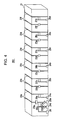
- Fig. 4 is a conceptual diagram showing an antenna device described in Japanese Unexamined Patent Application Publication No. 2004-328285 .
- a rectangular column-shaped base member 21 made of a dielectric material or a magnetic material, for example, six band-shaped radiation conductors 22a to 22f are divided and wound.
- Fig. 5 is an equivalent circuit diagram of the antenna device shown in Fig. 4.
- the radiation conductor 22a is connected between the varactor diodes 23a and 23b, and the radiation conductor 22b is connected between the varactor diodes 23b and 23c.
- the varactor diode 23f is connected between the radiation conductors 22e and 22f.
- the varactors are arranged such that adjacent varactors have opposite polarities.
- the radiation conductor 22a is connected between anodes of the varactor diodes 23a and 23b, which are located on a feed end side.
- the radiation conductor 22b is connected between cathodes of the varactor diodes 23b and 23c.
- the radiation conductor 22c is connected between anodes of the varactor diodes 23c and 23d.
- the radiation conductor 22d is connected between cathodes of the varactor diodes 23d and 23e.
- the radiation conductor 22e is connected between anodes of the varactor diodes 23e and 23f.
- the radiation conductor 22f connected to the cathode of the varactor diode 23f serves as a discharge end.
- the above-mentioned varactor diodes 23 are provided on a side of the base member 21.
- first electrodes 24a to 24c for grounding the anodes of the varactor diodes 23 and second electrodes 25a to 25d for applying tuning voltages to the cathodes of the varactor diodes are formed on the side of the base member 21.
- Substantially central parts of the radiation conductors 22a, 22c, and 22e are connected to the first electrodes 24a, 24b, and 24c through resistors 26a, 26b, and 26c, respectively.
- a substantially central part of the cathode of the varactor diode 23a and substantially central parts of the radiation conductors 22b, 22d, and 22f are connected to the second electrodes 25a to 25d through resistors 27a, 27b, 27c, and 27d, respectively.
- the above-mentioned resistors 26 and 27 are also provided on the side of the base member 21.
- a third electrode 28 for supplying a signal and a first electrode 24d for grounding are also formed on the side of the base member 21.
- the cathode of the varactor diode 23a which is located on the feed end side, is connected to the third electrode 28 though an impedance-matching circuit 30.
- the impedance-matching circuit 30 includes an inductance element 30a, which is connected between the cathode of the varactor diode 23a and the third electrode 28, and a capacitance element 30b, which is connected between the third electrode 28 and the first electrode 24d.
- the inductance element 30a and the capacitance element 30b are also provided on the side of the base member 21.
- the inductance element 30a is not necessarily provided. If the inductance element 30a is not provided, the cathode of the varactor diode located on the feed end side can be directly connected to the third electrode 28.
- Fig. 6 is a schematic block diagram showing a receiver including an antenna device 200 configured as described above.
- An RF signal output from the antenna device 200 is input to a digital tuner unit 201.
- the digital tuner unit 201 performs frequency conversion of the RF signal, and tunes the signal into a reception channel.
- the digital tuner unit 201 inputs a digital reception signal in the reception channel to a demodulation circuit 202.
- the demodulation circuit 202 demodulates the digital reception signal and supplies demodulated data to an application processor 203 provided at the subsequent stage.
- the demodulation circuit 202 also generates a tuning voltage Vtune corresponding to a reception channel designated by an external device, and applies the tuning voltage Vtune to the second electrodes 25a to 25d of the antenna device 200.
- Resonance frequency characteristics and SWR characteristics of the antenna device 200 configured as described above are shown in Figs. 7A and 7B, respectively.
- the resonance frequency of the antenna device 200 increases as the tuning voltage Vtune applied to the second electrodes 25a to 25d increases.
- the antenna device 200 exhibits narrow band-pass characteristics at resonance frequencies (fl to fh), and the narrow band-pass characteristics are shifted by the tuning voltage Vtune.
- a broadcasting band covers a range between 470 MHz and 770 MHz
- a broadcasting band (a range between 470 MHz and 770 MHz) is divided into a plurality of resonance frequencies (narrow band-pass characteristics) and received, a wide range of frequencies can be received at an antenna having a relatively small size.
- tuning voltages applied for achieving resonance frequencies of respective reception channels and the respective reception channels have a one-to-one relationship.
- the demodulation circuit 202 When a broadcasting signal is received, the demodulation circuit 202 generates a tuning voltage Vtune corresponding to a reception channel, and applies the generated tuning voltage Vtune as a preset voltage to the second electrodes 25a to 25d.
- the antenna device 200 has a resonance frequency corresponding to the tuning voltage Vtune, thus being capable of receiving a reception signal in the reception channel.
- a tuning voltage Vtune applied for a reception channel from the demodulation circuit 202 to the antenna device 200 is a fixed voltage set in advance, when a resonance frequency is shifted due to a change in usage or environment of the antenna device 200, reception quality is deteriorated.
- Vtune V1
- the signal level of a demodulated reception signal exhibits a shape in which the right shoulder drops, as shown in Fig. 8B. If the signal level of a reception signal is distorted and exhibits a shape in which the right shoulder drops or the left shoulder drops, a problem may occur in that a playback image played back by the application processor 203 on the basis of the reception signal is stopped or playback sound is distorted.
- the present invention provides a digital signal receiver that is capable of correcting a shift of a resonance frequency and improving reception quality even when the resonance frequency is shifted from a desired position due to a change in usage or environment of an antenna device.
- a digital signal receiver includes an antenna device including a resonance circuit formed by a radiation conductor and a variable capacitance element coupled to the radiation conductor and resonating at a resonance frequency corresponding to a tuning voltage supplied to the variable capacitance element; a digital tuner unit connected at a subsequent stage of the antenna device and receiving a digital signal in a reception channel having a predetermined bandwidth; a demodulation unit demodulating a digital reception signal that has been subjected to multicarrier modulation output from the digital tuner unit; antenna tuning control means for supplying to the antenna device a tuning voltage corresponding to the reception channel; and correction means for detecting levels of a plurality of carriers in the bandwidth of the reception channel and for correcting the tuning voltage so as to reduce a level difference between the carriers to a predetermined value or less.
- the digital signal is a digital television signal
- the plurality of carriers are carriers of a spread pilot signal.
- the shift of the resonance frequency can be corrected, thus achieving an improvement in reception quality.
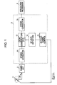
- Fig. 1 is a functional block diagram showing a digital signal receiver according to an embodiment of the present invention.
- the digital signal receiver according to this embodiment includes an antenna device 1 tunable over a wide range of frequencies, a digital tuner unit 2 performing frequency conversion of an RF signal, which is a reception signal output from the antenna device 1, tuning the signal into a reception channel, and outputting a digital reception signal, and a demodulation circuit 3 demodulating the digital reception signal output from the digital tuner unit 2.
- the digital signal receiver outputs the demodulated digital signal to an application processor 4 provided at the subsequent stage.
- the antenna device 1 contains radiation conductors and variable capacitance elements coupled to the radiation conductors.
- the antenna device 1 is capable of resonating with respect to a reception signal.
- the antenna device 1 can be configured similarly to the antenna device 200 shown in Figs. 4 and 5.
- the antenna device 1 has the same configuration as the above-described antenna device 200, and the configuration of the antenna device 1 will be described using the reference numerals shown in Figs. 4 and 5 in an appropriate manner.
- the demodulation circuit 3 includes a symbol extraction unit 11 extracting symbols from a digital reception signal, an orthogonal frequency-division multiplexing (OFDM) demodulation unit 12 demodulating extracted symbol data by performing FFT (fast Fourier transform) processing, and an error correction unit 13 correcting demodulated data obtained by OFDM demodulation.
- OFDM orthogonal frequency-division multiplexing
- the demodulation circuit 3 includes an SP level detection unit 14 serving as correction means having a function of correcting a tuning voltage so as to reduce a level difference between a plurality of carriers in the bandwidth of a reception signal to a predetermined value or less and an antenna tuning control unit 15 correcting a tuning voltage set in advance so as to correspond to the reception signal using a correction amount designated by the SP level detection unit 14 and outputting the corrected tuning voltage.
- an SP level detection unit 14 serving as correction means having a function of correcting a tuning voltage so as to reduce a level difference between a plurality of carriers in the bandwidth of a reception signal to a predetermined value or less
- an antenna tuning control unit 15 correcting a tuning voltage set in advance so as to correspond to the reception signal using a correction amount designated by the SP level detection unit 14 and outputting the corrected tuning voltage.
- a modulation method for transmission data for example, Japanese integrated services of digital broadcasting-terrestrial (ISDB-T)
- ISDB-T Japanese integrated services of digital broadcasting-terrestrial
- a pilot signal hereinafter, referred to as a "spread pilot signal SP" is arranged for each twelve carriers.
- the inclination of signal level of spread pilot signals SP exhibits a shape in which the right shoulder drops.
- demodulated multicarriers exhibit a shape in which the left shoulder drops
- the inclination of spread pilot signals SP exhibits a shape in which the left shoulder drops.
- the inclination of signal level of spread pilot signals SP indicates that the current resonance frequency is shifted from the original frequency.
- the direction of the inclination of signal level of spread pilot signals SP indicates that the direction toward which the resonance frequency is shifted from the original frequency fl.
- the polarity of the obtained difference D indicates an inclination direction
- the value obtained by dividing the absolute value of the difference D by a pilot interval (P1-P2) indicates the width of a shift, which is the magnitude of inclination.
- the SP level detection unit 14 calculates a correction amount ⁇ V so that uniform signal levels of the spread pilot signals SP can be achieved over the bandwidth of the reception channel. That is, a difference D between spread pilot signals SP is compared with a threshold, and a correction amount that allows the difference D to be reduced to the threshold or less is determined.
- the antenna device 1 exhibits narrow-band characteristics in which a resonance frequency (f1- ⁇ ), which is shifted from the desired resonance frequency fl, serves as a center frequency, and an RF reception signal received in accordance with the narrow-band characteristics is output from a discharge end (the radiation conductor 22f) to the digital tuner unit 2.
- the digital tuner unit 2 performs frequency conversion for the RF reception signal to be converted into an intermediate-frequency signal.
- the digital tuner unit 2 also tunes the signal into a reception channel, and outputs a digital reception signal including a signal component shifted from the reception channel by the predetermined amount.
- the symbol extraction unit 11 extracts symbols from the digital reception signal, and the OFDM demodulation unit 12 performs OFDM demodulation.
- Demodulated data obtained here exhibits frequency characteristics exhibiting a shape in which the right shoulder drops, as shown in Fig. 2B.
- the SP level detection unit 14 calculates a difference D on the basis of signal levels of a plurality of spread pilot signals SP set in advance. On the basis of the calculated difference D, the SP level detection unit 14 calculates a correction amount ⁇ V that achieves uniform signal level at least in the bandwidth of the reception channel, and reports the correction amount ⁇ V to the antenna tuning control unit 15.
- Vtune V1 + correction amount ⁇ V
- the signal level of demodulated data obtained by OFDM demodulation by the OFDM demodulation unit 12 exhibits a flat shape, as shown in Fig. 3B.
- the difference D calculated by the SP level detection unit 14 is smaller than or equal to the threshold.
- the SP level detection unit 14 maintains the current tuning voltage Vtune, and does not perform further correction.
- the inclination of signal levels is detected on the basis of a difference D between a plurality of spread pilot signals SP, and a tuning voltage Vtune is corrected using a correction amount ⁇ V, which allows the difference D between the spread pilot signals SP to be reduced to the threshold or less.
- a correction amount ⁇ V which allows the difference D between the spread pilot signals SP to be reduced to the threshold or less.
- the inclination of signal levels is detected on the basis of a difference between a plurality of spread pilot signals SP in the above description, spread pilot signals SP are not necessarily used in the present invention.
- Information or other carriers such as control carriers, may be used.
- detection of the inclination of signal levels is not necessarily performed using a difference method.
- the inclination of signal levels may be detected using any other detection principles, such as differentiation or detection.
- the present invention is applicable to a digital signal receiver presetting a tuning voltage suitable for a reception channel for an antenna device.
Landscapes
- Input Circuits Of Receivers And Coupling Of Receivers And Audio Equipment (AREA)
- Superheterodyne Receivers (AREA)
Abstract
Description
- This application claims benefit of the
Japanese Patent Application No. 2006-147697 filed on May 29, 2006 - The present invention relates to a digital signal receiver including an antenna device tunable over a wide range of frequencies.
- An antenna device that contains radiation conductors and variable capacitance elements coupled to the radiation conductors and that is tunable over a wide range of frequencies is available (for example, see
Japanese Unexamined Patent Application Publication No. 2004-328285 - Fig. 4 is a conceptual diagram showing an antenna device described in
Japanese Unexamined Patent Application Publication No. 2004-328285 shaped base member 21 made of a dielectric material or a magnetic material, for example, six band-shaped radiation conductors 22a to 22f are divided and wound. Theradiation conductors 22a to 22f andvaractor diodes 23a to 23f, which are variable capacitance elements and whose number is equal to the number of radiation conductors, are disposed alternately and connected in series. - Fig. 5 is an equivalent circuit diagram of the antenna device shown in Fig. 4. The
radiation conductor 22a is connected between thevaractor diodes radiation conductor 22b is connected between thevaractor diodes varactor diode 23f is connected between theradiation conductors radiation conductor 22a is connected between anodes of thevaractor diodes radiation conductor 22b is connected between cathodes of thevaractor diodes radiation conductor 22c is connected between anodes of thevaractor diodes radiation conductor 22d is connected between cathodes of thevaractor diodes radiation conductor 22e is connected between anodes of thevaractor diodes radiation conductor 22f connected to the cathode of thevaractor diode 23f serves as a discharge end. The above-mentioned varactor diodes 23 are provided on a side of thebase member 21. - In addition, on the side of the
base member 21,first electrodes 24a to 24c for grounding the anodes of the varactor diodes 23 andsecond electrodes 25a to 25d for applying tuning voltages to the cathodes of the varactor diodes are formed. Substantially central parts of theradiation conductors first electrodes resistors varactor diode 23a and substantially central parts of theradiation conductors second electrodes 25a to 25d throughresistors base member 21. - A
third electrode 28 for supplying a signal and afirst electrode 24d for grounding are also formed on the side of thebase member 21. The cathode of thevaractor diode 23a, which is located on the feed end side, is connected to thethird electrode 28 though an impedance-matchingcircuit 30. The impedance-matchingcircuit 30 includes aninductance element 30a, which is connected between the cathode of thevaractor diode 23a and thethird electrode 28, and acapacitance element 30b, which is connected between thethird electrode 28 and thefirst electrode 24d. Theinductance element 30a and thecapacitance element 30b are also provided on the side of thebase member 21. Theinductance element 30a is not necessarily provided. If theinductance element 30a is not provided, the cathode of the varactor diode located on the feed end side can be directly connected to thethird electrode 28. - Fig. 6 is a schematic block diagram showing a receiver including an
antenna device 200 configured as described above. An RF signal output from theantenna device 200 is input to adigital tuner unit 201. Thedigital tuner unit 201 performs frequency conversion of the RF signal, and tunes the signal into a reception channel. Thedigital tuner unit 201 inputs a digital reception signal in the reception channel to ademodulation circuit 202. Thedemodulation circuit 202 demodulates the digital reception signal and supplies demodulated data to anapplication processor 203 provided at the subsequent stage. Thedemodulation circuit 202 also generates a tuning voltage Vtune corresponding to a reception channel designated by an external device, and applies the tuning voltage Vtune to thesecond electrodes 25a to 25d of theantenna device 200. - Resonance frequency characteristics and SWR characteristics of the
antenna device 200 configured as described above are shown in Figs. 7A and 7B, respectively. As shown in Fig. 7A, the resonance frequency of theantenna device 200 increases as the tuning voltage Vtune applied to thesecond electrodes 25a to 25d increases. In addition, as shown in Fig. 7B, theantenna device 200 exhibits narrow band-pass characteristics at resonance frequencies (fl to fh), and the narrow band-pass characteristics are shifted by the tuning voltage Vtune. - When wideband terrestrial digital broadcasting (in Japan, a broadcasting band covers a range between 470 MHz and 770 MHz) is received, if a broadcasting band (a range between 470 MHz and 770 MHz) is divided into a plurality of resonance frequencies (narrow band-pass characteristics) and received, a wide range of frequencies can be received at an antenna having a relatively small size. For example, the resonance frequency fl of the
antenna device 200 when the minimum tuning voltage, Vtune = V1, is applied is set to the lowest frequency (470 MHz) of the broadcasting band, the resonance frequency fh of theantenna device 200 when the maximum tuning voltage, Vtune = Vh, is applied is set to the highest frequency (770 MHz) of the broadcasting band, and tuning voltages applied for achieving resonance frequencies of respective reception channels and the respective reception channels have a one-to-one relationship. When a broadcasting signal is received, thedemodulation circuit 202 generates a tuning voltage Vtune corresponding to a reception channel, and applies the generated tuning voltage Vtune as a preset voltage to thesecond electrodes 25a to 25d. Theantenna device 200 has a resonance frequency corresponding to the tuning voltage Vtune, thus being capable of receiving a reception signal in the reception channel. - However, in the above-mentioned receiver of the related art, since a tuning voltage Vtune applied for a reception channel from the
demodulation circuit 202 to theantenna device 200 is a fixed voltage set in advance, when a resonance frequency is shifted due to a change in usage or environment of theantenna device 200, reception quality is deteriorated. - Fig. 8A shows a state in which an actual resonance frequency is shifted from a desired resonance frequency fl when a tuning voltage, Vtune = V1, is applied. For example, when the resonance frequency is shifted toward lower frequencies from the desired resonance frequency fl, the signal level of a demodulated reception signal exhibits a shape in which the right shoulder drops, as shown in Fig. 8B. If the signal level of a reception signal is distorted and exhibits a shape in which the right shoulder drops or the left shoulder drops, a problem may occur in that a playback image played back by the
application processor 203 on the basis of the reception signal is stopped or playback sound is distorted. - The present invention provides a digital signal receiver that is capable of correcting a shift of a resonance frequency and improving reception quality even when the resonance frequency is shifted from a desired position due to a change in usage or environment of an antenna device.
- A digital signal receiver according to an aspect of the present invention includes an antenna device including a resonance circuit formed by a radiation conductor and a variable capacitance element coupled to the radiation conductor and resonating at a resonance frequency corresponding to a tuning voltage supplied to the variable capacitance element; a digital tuner unit connected at a subsequent stage of the antenna device and receiving a digital signal in a reception channel having a predetermined bandwidth; a demodulation unit demodulating a digital reception signal that has been subjected to multicarrier modulation output from the digital tuner unit; antenna tuning control means for supplying to the antenna device a tuning voltage corresponding to the reception channel; and correction means for detecting levels of a plurality of carriers in the bandwidth of the reception channel and for correcting the tuning voltage so as to reduce a level difference between the carriers to a predetermined value or less.
- With this configuration, levels of a plurality of carriers in the bandwidth of a reception channel are detected, and a tuning voltage is corrected so as to reduce a level difference between the carriers to a predetermined value or less. Thus, even when a resonance frequency is shifted due to a change in usage or environment of the antenna device, the shift of the resonance frequency can be corrected, thus achieving an improvement in reception quality.
- In addition, in the digital signal receiver, the digital signal is a digital television signal, and the plurality of carriers are carriers of a spread pilot signal.
- Accordingly, even when a resonance frequency is shifted due to a change in usage or environment of an antenna device, the shift of the resonance frequency can be corrected, thus achieving an improvement in reception quality.
-
- Fig. 1 is a functional block diagram showing a digital signal receiver according to an embodiment of the present invention;
- Fig. 2A is a waveform chart showing a state of signal level of multicarriers in which spread pilot signals are arranged;
- Fig. 2B is a frequency characteristic diagram showing a state of signal level after OFDM demodulation is performed for the multicarriers shown in Fig. 2A;
- Fig. 3A illustrates a state of a corrected resonance frequency;
- Fig. 3B is a frequency characteristic diagram showing a state of signal level after OFDM demodulation is performed for a reception channel received at the resonance frequency shown in Fig. 3A;
- Fig. 4 is a schematic diagram showing an antenna device of the related art;
- Fig. 5 is an equivalent circuit diagram of the antenna device shown in Fig. 4;
- Fig. 6 is a functional block diagram showing a digital signal receiver of the related art;
- Fig. 7A is a characteristic diagram showing the relationship between a tuning voltage applied to the antenna device and a resonance frequency;
- Fig. 7B is an SWR characteristic diagram showing the relationship between a resonance frequency and the SWR;
- Fig. 8A illustrates SWR characteristics when a resonance frequency is shifted from the original position; and
- Fig. 8B is a frequency characteristic diagram showing a state of signal level after OFDM demodulation is performed for a reception channel received at the resonance frequency shown in Fig. 8A.
- Embodiments of the present invention will be described with reference to the attached drawings.
- Fig. 1 is a functional block diagram showing a digital signal receiver according to an embodiment of the present invention. As shown in Fig. 1, the digital signal receiver according to this embodiment includes an antenna device 1 tunable over a wide range of frequencies, a
digital tuner unit 2 performing frequency conversion of an RF signal, which is a reception signal output from the antenna device 1, tuning the signal into a reception channel, and outputting a digital reception signal, and ademodulation circuit 3 demodulating the digital reception signal output from thedigital tuner unit 2. The digital signal receiver outputs the demodulated digital signal to an application processor 4 provided at the subsequent stage. - The antenna device 1 contains radiation conductors and variable capacitance elements coupled to the radiation conductors. The antenna device 1 is capable of resonating with respect to a reception signal. The antenna device 1 can be configured similarly to the
antenna device 200 shown in Figs. 4 and 5. In this embodiment, the antenna device 1 has the same configuration as the above-describedantenna device 200, and the configuration of the antenna device 1 will be described using the reference numerals shown in Figs. 4 and 5 in an appropriate manner. - The
demodulation circuit 3 includes asymbol extraction unit 11 extracting symbols from a digital reception signal, an orthogonal frequency-division multiplexing (OFDM)demodulation unit 12 demodulating extracted symbol data by performing FFT (fast Fourier transform) processing, and anerror correction unit 13 correcting demodulated data obtained by OFDM demodulation. In addition, in this embodiment, thedemodulation circuit 3 includes an SPlevel detection unit 14 serving as correction means having a function of correcting a tuning voltage so as to reduce a level difference between a plurality of carriers in the bandwidth of a reception signal to a predetermined value or less and an antennatuning control unit 15 correcting a tuning voltage set in advance so as to correspond to the reception signal using a correction amount designated by the SPlevel detection unit 14 and outputting the corrected tuning voltage. - The relationship between the inclination of reception signal level and a shift from a desired resonance frequency will be described with reference to Figs. 2A and 2B. In the current terrestrial digital television broadcasting (for example, Japanese integrated services of digital broadcasting-terrestrial (ISDB-T)), an OFDM modulation method, which is one of multicarrier modulation methods, is adopted as a modulation method for transmission data. In this method, 5617 carriers are used as modulation carriers, and a pilot signal (hereinafter, referred to as a "spread pilot signal SP") is arranged for each twelve carriers.
- For example, if a resonance frequency set by the tuning voltage, Vtune = V1, is shifted toward lower frequencies from the original frequency fl (see Fig. 8A), multicarriers in the bandwidth of a reception channel exhibit a shape in which the right shoulder drops, as shown in Fig. 2A, and the signal level of a demodulated reception channel also exhibits a shape in which the right shoulder drops, as shown in Fig. 2B.
- When attention is focused on spread pilot signals SP that are substantially uniformly spread over the multicarriers, it is clear that, similarly to the inclination of all the multicarriers, the inclination of signal level of spread pilot signals SP exhibits a shape in which the right shoulder drops. When the resonance frequency of the antenna device 1 is shifted toward higher frequencies from the original frequency f1, demodulated multicarriers exhibit a shape in which the left shoulder drops, and similarly to the inclination of all the multicarriers, the inclination of spread pilot signals SP exhibits a shape in which the left shoulder drops. The inclination of signal level of spread pilot signals SP indicates that the current resonance frequency is shifted from the original frequency. The direction of the inclination of signal level of spread pilot signals SP indicates that the direction toward which the resonance frequency is shifted from the original frequency fl.
- The SP
level detection unit 14 detects signal levels of all the spread pilot signals SP or a predetermined number of spread pilot signals SP at least in the bandwidth of a reception channel, obtains a correction amount ΔV for the current tuning voltage, Vtune = V1, on the basis of the inclination of the detected signal levels, and reports the correction amount ΔV to the antennatuning control unit 15. For example, a difference D between the signal level of a spread pilot signal SP at a disposed position P1 and the signal level of a spread pilot signal SP at a disposed position P2, which is distant from the disposed position P1 by a predetermined frequency, is obtained. The polarity of the obtained difference D indicates an inclination direction, and the value obtained by dividing the absolute value of the difference D by a pilot interval (P1-P2) indicates the width of a shift, which is the magnitude of inclination. Thus, in accordance with the polarity of the difference D and the magnitude of the inclination, it is determined which direction (upward or downward) and what degree correction is to be made from the current tuning voltage. Increasing the number of spread pilot signals SP causes the detection accuracy to increase. It is desirable that the number of spread pilot signals SP and the disposed positions of the spread pilot signals SP are set so as to correspond to a desired detection accuracy. In accordance with a calculated difference D between signal levels of a plurality of spread pilot signals SP set in advance, the SPlevel detection unit 14 calculates a correction amount ΔV so that uniform signal levels of the spread pilot signals SP can be achieved over the bandwidth of the reception channel. That is, a difference D between spread pilot signals SP is compared with a threshold, and a correction amount that allows the difference D to be reduced to the threshold or less is determined. - The antenna
tuning control unit 15 corrects a tuning voltage (fixed voltage before correction) set in advance in accordance with a channel selection signal, which is not shown, using a correction amount ΔV designated by the SPlevel detection unit 14, generates a corrected tuning voltage, Vtune = V1 + correction amount ΔV, and applies the corrected tuning voltage to the antenna device 1. - An operation in this embodiment configured as described above is described next.
- The antenna
tuning control unit 15 generates a tuning voltage, Vtune = V1, which is a fixed voltage before correction set in advance in accordance with a channel selection signal, and applies the tuning voltage, Vtune = V1, to thesecond electrodes 25a to 25d of the antenna device 1. The resonance frequency of the antenna device 1 changes in accordance with the tuning voltage, Vtune = V1, applied to thesecond electrodes 25a to 25d. Here, it is assumed that, when the tuning voltage, Vtune = V1, is applied, the resonance frequency is shifted toward lower frequencies from a desired resonance frequency fl by a predetermined amount, as shown in Fig. 8A. The antenna device 1 exhibits narrow-band characteristics in which a resonance frequency (f1-α), which is shifted from the desired resonance frequency fl, serves as a center frequency, and an RF reception signal received in accordance with the narrow-band characteristics is output from a discharge end (theradiation conductor 22f) to thedigital tuner unit 2. Thedigital tuner unit 2 performs frequency conversion for the RF reception signal to be converted into an intermediate-frequency signal. Thedigital tuner unit 2 also tunes the signal into a reception channel, and outputs a digital reception signal including a signal component shifted from the reception channel by the predetermined amount. - In the
demodulation circuit 3, thesymbol extraction unit 11 extracts symbols from the digital reception signal, and theOFDM demodulation unit 12 performs OFDM demodulation. Demodulated data obtained here exhibits frequency characteristics exhibiting a shape in which the right shoulder drops, as shown in Fig. 2B. The SPlevel detection unit 14 calculates a difference D on the basis of signal levels of a plurality of spread pilot signals SP set in advance. On the basis of the calculated difference D, the SPlevel detection unit 14 calculates a correction amount ΔV that achieves uniform signal level at least in the bandwidth of the reception channel, and reports the correction amount ΔV to the antennatuning control unit 15. The antennatuning control unit 15 generates a corrected tuning voltage, Vtune = V1 + correction amount ΔV, which is obtained by correcting the current tuning voltage V1 using the correction amount ΔV, and applies the corrected tuning voltage, Vtune = V1 + correction amount ΔV, to the antenna device 1. - The resonance frequency of the antenna device 1 is shifted to the original frequency fl, as shown in Fig. 3A, due to the application of the corrected tuning voltage, Vtune = V1 + correction amount ΔV, to the
second electrodes 25a to 25d. Thus, since the actual resonance frequency of the antenna device 1 is equal to the frequency f1, the currently selected reception channel can be received without loss. As a result, the signal level of demodulated data obtained by OFDM demodulation by theOFDM demodulation unit 12 exhibits a flat shape, as shown in Fig. 3B. - If the signal level of demodulated data forms a flat shape, as shown in Fig. 3B, the difference D calculated by the SP
level detection unit 14 is smaller than or equal to the threshold. When the difference D is smaller than or equal to the threshold, the SPlevel detection unit 14 maintains the current tuning voltage Vtune, and does not perform further correction. - As described above, according to this embodiment, the inclination of signal levels is detected on the basis of a difference D between a plurality of spread pilot signals SP, and a tuning voltage Vtune is corrected using a correction amount ΔV, which allows the difference D between the spread pilot signals SP to be reduced to the threshold or less. Thus, even when a resonance frequency is shifted due to a change in usage or environment of the antenna device 1, the shift of the resonance frequency can be corrected, thus achieving an improvement of reception quality.
- Although the inclination of signal levels is detected on the basis of a difference between a plurality of spread pilot signals SP in the above description, spread pilot signals SP are not necessarily used in the present invention. Information or other carriers, such as control carriers, may be used. In addition, detection of the inclination of signal levels is not necessarily performed using a difference method. The inclination of signal levels may be detected using any other detection principles, such as differentiation or detection.
- The present invention is applicable to a digital signal receiver presetting a tuning voltage suitable for a reception channel for an antenna device.
Claims (2)
- A digital signal receiver comprising:an antenna device including a resonance circuit formed by a radiation conductor and a variable capacitance element coupled to the radiation conductor and resonating at a resonance frequency corresponding to a tuning voltage supplied to the variable capacitance element;a digital tuner unit connected at a subsequent stage of the antenna device and receiving a digital signal in a reception channel having a predetermined bandwidth;a demodulation unit demodulating a digital reception signal that has been subjected to multicarrier modulation output from the digital tuner unit;antenna tuning control means for supplying to the antenna device a tuning voltage corresponding to the reception channel; andcorrection means for detecting levels of a plurality of carriers in the bandwidth of the reception channel and for correcting the tuning voltage so as to reduce a level difference between the carriers to a predetermined value or less.
- The digital signal receiver according to Claim 1, wherein the digital signal is a digital television signal, and the plurality of carriers are carriers of a spread pilot signal.
Applications Claiming Priority (1)
| Application Number | Priority Date | Filing Date | Title |
|---|---|---|---|
| JP2006147697A JP2007318585A (en) | 2006-05-29 | 2006-05-29 | Digital signal receiver |
Publications (1)
| Publication Number | Publication Date |
|---|---|
| EP1863127A1 true EP1863127A1 (en) | 2007-12-05 |
Family
ID=38457702
Family Applications (1)
| Application Number | Title | Priority Date | Filing Date |
|---|---|---|---|
| EP07010380A Withdrawn EP1863127A1 (en) | 2006-05-29 | 2007-05-24 | Digital signal receiver including wideband tunable antenna device |
Country Status (4)
| Country | Link |
|---|---|
| US (1) | US7817749B2 (en) |
| EP (1) | EP1863127A1 (en) |
| JP (1) | JP2007318585A (en) |
| CN (1) | CN101083476B (en) |
Cited By (1)
| Publication number | Priority date | Publication date | Assignee | Title |
|---|---|---|---|---|
| FR2985623A1 (en) * | 2012-01-05 | 2013-07-12 | Korea Electronics Telecomm | CHANNEL TUNING DEVICE AND METHOD USING A SPREAD SPECTRUM IN A DIGITAL BROADCASTING SYSTEM |
Families Citing this family (4)
| Publication number | Priority date | Publication date | Assignee | Title |
|---|---|---|---|---|
| ATE466342T1 (en) * | 2006-07-18 | 2010-05-15 | Ericsson Telefon Ab L M | FOLDING OF INPUT DATA VALUES FOR A TRANSFORMATION |
| JP5161657B2 (en) * | 2008-05-29 | 2013-03-13 | 京セラ株式会社 | Mobile communication terminal |
| CN104980183B (en) * | 2014-04-02 | 2018-09-07 | 中芯国际集成电路制造(上海)有限公司 | Wireless transmitting and receiving device and method |
| HUE040669T2 (en) * | 2015-07-15 | 2019-03-28 | Grieshaber Vega Kg | Fill level measurement device |
Citations (7)
| Publication number | Priority date | Publication date | Assignee | Title |
|---|---|---|---|---|
| WO1988005214A1 (en) * | 1987-01-02 | 1988-07-14 | Motorola, Inc. | Automatic antenna tuning system for portable communication devices |
| DE19619715A1 (en) * | 1995-05-19 | 1996-11-21 | Prince Corp | Learnable transceiver |
| JPH114469A (en) * | 1997-06-13 | 1999-01-06 | Kokusai Electric Co Ltd | Radio paging receiver |
| WO2001089036A1 (en) | 2000-05-18 | 2001-11-22 | Siemens Aktiengesellschaft | Device and method for frequency tuning of an antenna for sending and receiving signals |
| JP2004328285A (en) | 2003-04-23 | 2004-11-18 | Alps Electric Co Ltd | Mobile receiver |
| EP1557902A1 (en) * | 2004-01-26 | 2005-07-27 | Alps Electric Co., Ltd. | Wideband tunable antenna |
| JP2006147697A (en) | 2004-11-17 | 2006-06-08 | Hitachi Metals Ltd | Conductive ball array mask and method of manufacturing the same |
Family Cites Families (13)
| Publication number | Priority date | Publication date | Assignee | Title |
|---|---|---|---|---|
| US5136719A (en) * | 1988-12-05 | 1992-08-04 | Seiko Corp. | Automatic antenna tubing method and apparatus |
| US5483688A (en) * | 1993-01-22 | 1996-01-09 | Seiko Communications Holding N.V. | Adaptive automatic antenna tuning method and apparatus |
| KR950015100B1 (en) * | 1993-03-13 | 1995-12-21 | 엘지전자주식회사 | Fine tuning device for tuning data and adjustment method of TV receiver |
| US5654766A (en) * | 1995-06-29 | 1997-08-05 | Philips Electronics North America Corporation | Television tuning systems and methods employing use of ghost cancellation and antenna directionality control to produce a ghost-free television signal |
| JP2888179B2 (en) * | 1995-08-24 | 1999-05-10 | 日本電気株式会社 | Antenna tuning controller |
| JP3145054B2 (en) * | 1997-05-15 | 2001-03-12 | 富士通テン株式会社 | Orthogonal frequency division multiplexing receiver |
| JP2000174651A (en) * | 1998-12-09 | 2000-06-23 | Sony Corp | Shortwave receiver and its antenna adapter |
| JP3717741B2 (en) | 2000-03-21 | 2005-11-16 | 株式会社ユーシン | Automatic tuning antenna system |
| JP3953333B2 (en) * | 2002-02-14 | 2007-08-08 | パイオニア株式会社 | Receiving apparatus and method thereof |
| JP4287686B2 (en) * | 2003-03-31 | 2009-07-01 | パナソニック株式会社 | Multi-carrier receiver and line compensation method |
| JP4060746B2 (en) * | 2003-04-18 | 2008-03-12 | 株式会社ヨコオ | Variable tuning antenna and portable radio using the same |
| CN100379157C (en) * | 2003-06-24 | 2008-04-02 | 松下电器产业株式会社 | High-frequency receiving device, integrated circuit for use therein, and television receiver |
| JP4128166B2 (en) * | 2004-09-24 | 2008-07-30 | 三洋電機株式会社 | ANTENNA CONTROL DEVICE, ANTENNA CONTROL METHOD, AND DIGITAL RECEIVING DEVICE |
-
2006
- 2006-05-29 JP JP2006147697A patent/JP2007318585A/en active Pending
-
2007
- 2007-05-24 EP EP07010380A patent/EP1863127A1/en not_active Withdrawn
- 2007-05-25 US US11/807,213 patent/US7817749B2/en not_active Expired - Fee Related
- 2007-05-28 CN CN2007101063648A patent/CN101083476B/en not_active Expired - Fee Related
Patent Citations (7)
| Publication number | Priority date | Publication date | Assignee | Title |
|---|---|---|---|---|
| WO1988005214A1 (en) * | 1987-01-02 | 1988-07-14 | Motorola, Inc. | Automatic antenna tuning system for portable communication devices |
| DE19619715A1 (en) * | 1995-05-19 | 1996-11-21 | Prince Corp | Learnable transceiver |
| JPH114469A (en) * | 1997-06-13 | 1999-01-06 | Kokusai Electric Co Ltd | Radio paging receiver |
| WO2001089036A1 (en) | 2000-05-18 | 2001-11-22 | Siemens Aktiengesellschaft | Device and method for frequency tuning of an antenna for sending and receiving signals |
| JP2004328285A (en) | 2003-04-23 | 2004-11-18 | Alps Electric Co Ltd | Mobile receiver |
| EP1557902A1 (en) * | 2004-01-26 | 2005-07-27 | Alps Electric Co., Ltd. | Wideband tunable antenna |
| JP2006147697A (en) | 2004-11-17 | 2006-06-08 | Hitachi Metals Ltd | Conductive ball array mask and method of manufacturing the same |
Cited By (1)
| Publication number | Priority date | Publication date | Assignee | Title |
|---|---|---|---|---|
| FR2985623A1 (en) * | 2012-01-05 | 2013-07-12 | Korea Electronics Telecomm | CHANNEL TUNING DEVICE AND METHOD USING A SPREAD SPECTRUM IN A DIGITAL BROADCASTING SYSTEM |
Also Published As
| Publication number | Publication date |
|---|---|
| CN101083476A (en) | 2007-12-05 |
| JP2007318585A (en) | 2007-12-06 |
| US20070291877A1 (en) | 2007-12-20 |
| CN101083476B (en) | 2010-09-29 |
| US7817749B2 (en) | 2010-10-19 |
Similar Documents
| Publication | Publication Date | Title |
|---|---|---|
| US8208522B2 (en) | System and methods for receiving OFDM symbols having timing and frequency offsets | |
| US6788349B2 (en) | Method and system for broadcasting a digital data signal within an analog TV signal using Orthogonal Frequency Division Multiplexing | |
| US7817749B2 (en) | Digital signal receiver including wideband tunable antenna device | |
| JP5075212B2 (en) | Apparatus and method for classifying modulation in a multipath environment | |
| EP2346222B1 (en) | Receiving apparatus, method and program | |
| CN1551515A (en) | Tuner | |
| JP2009049868A (en) | Tunable antenna module with frequency correction circuit and manufacturing method thereof | |
| EP2151076A2 (en) | System and method for scheduling and transferring data through a transmission system | |
| KR20170093119A (en) | Method and apparatus for transmitting a-priori information in a communication system | |
| US8311155B2 (en) | Electronic tuner and high frequency receiving device using the same | |
| WO2009128222A1 (en) | Receiver and electronic device using the same | |
| US20080247476A1 (en) | Method and Synchronizer for Fine Ofdm Symbol Synchronization and Method/Receiver for the Reception of Ofdm Symbols | |
| CN101998080B (en) | Receiving apparatus and receiving method | |
| CN1157939C (en) | TV/FM (Television/Frequency Modulation) Receiver for Multimedia Applications | |
| US20230254194A1 (en) | Communication device and method for radio frequency communication | |
| JP2005136471A (en) | OFDM receiving apparatus using diversity, OFDM receiving circuit using diversity, and OFDM receiving method using diversity | |
| CN1292539C (en) | Digital tuner | |
| EP2587797A1 (en) | Channel scan apparatus and channel scan method for co-scanning different television signals in selected radio frequency channel | |
| JP3955550B2 (en) | Modulation error ratio measuring device | |
| JP3841665B2 (en) | OFDM signal reception quality evaluation apparatus and its reception quality evaluation method | |
| EP1986427A2 (en) | Channel list forming method, receiving apparatus, picture display apparatus, sound output apparatus, and reception setting method | |
| US9288095B1 (en) | Signal receiving system, band detection method for multi-carrier signal and demodulating apparatus thereof | |
| JP2010213061A (en) | Receiver | |
| EP3758367B1 (en) | Signal quality sensor, tv set and method for determinig tv signal quality | |
| JP2004266747A (en) | Modulation error ratio measuring apparatus |
Legal Events
| Date | Code | Title | Description |
|---|---|---|---|
| PUAI | Public reference made under article 153(3) epc to a published international application that has entered the european phase |
Free format text: ORIGINAL CODE: 0009012 |
|
| AK | Designated contracting states |
Kind code of ref document: A1 Designated state(s): AT BE BG CH CY CZ DE DK EE ES FI FR GB GR HU IE IS IT LI LT LU LV MC MT NL PL PT RO SE SI SK TR |
|
| AX | Request for extension of the european patent |
Extension state: AL BA HR MK YU |
|
| 17P | Request for examination filed |
Effective date: 20080331 |
|
| AKX | Designation fees paid |
Designated state(s): DE FR GB |
|
| 17Q | First examination report despatched |
Effective date: 20120210 |
|
| STAA | Information on the status of an ep patent application or granted ep patent |
Free format text: STATUS: THE APPLICATION IS DEEMED TO BE WITHDRAWN |
|
| 18D | Application deemed to be withdrawn |
Effective date: 20120621 |