EP1863039A2 - Conductor with non-circular cross-section - Google Patents
Conductor with non-circular cross-section Download PDFInfo
- Publication number
- EP1863039A2 EP1863039A2 EP07252241A EP07252241A EP1863039A2 EP 1863039 A2 EP1863039 A2 EP 1863039A2 EP 07252241 A EP07252241 A EP 07252241A EP 07252241 A EP07252241 A EP 07252241A EP 1863039 A2 EP1863039 A2 EP 1863039A2
- Authority
- EP
- European Patent Office
- Prior art keywords
- ridges
- conductor
- insulator
- depressions
- corrugated
- Prior art date
- Legal status (The legal status is an assumption and is not a legal conclusion. Google has not performed a legal analysis and makes no representation as to the accuracy of the status listed.)
- Withdrawn
Links
- 239000004020 conductor Substances 0.000 title claims abstract description 57
- 238000004891 communication Methods 0.000 claims abstract description 12
- 239000012212 insulator Substances 0.000 claims description 36
- 238000009413 insulation Methods 0.000 abstract description 9
- 239000000463 material Substances 0.000 description 8
- 230000007423 decrease Effects 0.000 description 7
- 230000003247 decreasing effect Effects 0.000 description 4
- 238000010276 construction Methods 0.000 description 2
- 230000002238 attenuated effect Effects 0.000 description 1
- 230000008878 coupling Effects 0.000 description 1
- 238000010168 coupling process Methods 0.000 description 1
- 238000005859 coupling reaction Methods 0.000 description 1
- 230000002500 effect on skin Effects 0.000 description 1
- 230000005672 electromagnetic field Effects 0.000 description 1
- 238000000034 method Methods 0.000 description 1
- 239000000203 mixture Substances 0.000 description 1
- 238000012986 modification Methods 0.000 description 1
- 230000004048 modification Effects 0.000 description 1
- 230000002093 peripheral effect Effects 0.000 description 1
- 230000001629 suppression Effects 0.000 description 1
Images



Classifications
-
- H—ELECTRICITY
- H01—ELECTRIC ELEMENTS
- H01B—CABLES; CONDUCTORS; INSULATORS; SELECTION OF MATERIALS FOR THEIR CONDUCTIVE, INSULATING OR DIELECTRIC PROPERTIES
- H01B11/00—Communication cables or conductors
-
- H—ELECTRICITY
- H01—ELECTRIC ELEMENTS
- H01B—CABLES; CONDUCTORS; INSULATORS; SELECTION OF MATERIALS FOR THEIR CONDUCTIVE, INSULATING OR DIELECTRIC PROPERTIES
- H01B7/00—Insulated conductors or cables characterised by their form
- H01B7/0009—Details relating to the conductive cores
-
- H—ELECTRICITY
- H01—ELECTRIC ELEMENTS
- H01B—CABLES; CONDUCTORS; INSULATORS; SELECTION OF MATERIALS FOR THEIR CONDUCTIVE, INSULATING OR DIELECTRIC PROPERTIES
- H01B7/00—Insulated conductors or cables characterised by their form
- H01B7/02—Disposition of insulation
- H01B7/0233—Cables with a predominant gas dielectric
-
- H—ELECTRICITY
- H01—ELECTRIC ELEMENTS
- H01B—CABLES; CONDUCTORS; INSULATORS; SELECTION OF MATERIALS FOR THEIR CONDUCTIVE, INSULATING OR DIELECTRIC PROPERTIES
- H01B11/00—Communication cables or conductors
- H01B11/002—Pair constructions
Definitions
- the dielectric constant is a key parameter in the construction of high performance cable. It can be inversely proportional to the signal throughput and directly proportional to the attenuation values when the cable design is properly optimized. Generally, as the dielectric constant decreases, the signal throughput increases and the signal attenuation values decrease all attributed to the cable dimensional design that can be more favorably optimized. Thus, a lower dielectric constant can result in a stronger signal arriving more quickly with less distortion and less delay skew.
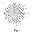
- FIG. 1 is a cross-sectional view of a wire according to one embodiment of the present invention
- FIG. 3 is a cross-sectional view of a twisted wire pair according to the embodiment of FIG. 1;
- a wire 50 is illustrated having a non-circular conductor 52 and an insulator 54.
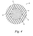
- the conductor 52 includes ridges 56 and depressions 57, which creates air gaps 58.
- the insulator 54 is a smooth circular surface, with no ridges or depressions. The air gaps 58 reduce the overall dielectric constant of the material between the conductors 52.
Landscapes
- Communication Cables (AREA)
- Insulated Conductors (AREA)
Abstract
Description
- This application claims priority to
U.S. Provisional Application Serial No. 60/803,639, filed on June 1, 2006 - The present invention relates generally to communications cables and more specifically relates to apparatus and methods for reducing the net dielectric constant of the wire insulation.
- Suppression of alien crosstalk in communication systems is an increasingly important practice for improving systems' reliability and the quality of communication. As the bandwidth of communication systems increases, so does the importance of reducing or eliminating alien crosstalk.
- In wired communication systems, crosstalk is caused by electromagnetic interference within a communication cable or between cables. Crosstalk coupling between pairs is proportional to the dielectric constant of the material separating the two pairs. Therefore, decreasing the overall dielectric constant of the material between the conductors decreases the crosstalk between the pairs. There will also be a resulting decrease in alien crosstalk between adjacent communication cables having decreased overall dielectric constants for the materials separating the conductors.
- The dielectric constant is a key parameter in the construction of high performance cable. It can be inversely proportional to the signal throughput and directly proportional to the attenuation values when the cable design is properly optimized. Generally, as the dielectric constant decreases, the signal throughput increases and the signal attenuation values decrease all attributed to the cable dimensional design that can be more favorably optimized. Thus, a lower dielectric constant can result in a stronger signal arriving more quickly with less distortion and less delay skew.
- Therefore, there is a need to reduce the overall dielectric constant of the material that separates conductors in a cable in order to reduce crosstalk and delay skew and provide stronger, less attenuated signals.
- According to one embodiment of the present invention, air gaps are provided to decrease the overall dielectric constant of the material between conductors in a corrugated cable.
- According to some embodiments of the present invention, a conductor is corrugated to provide air gaps between the conductor and insulation.
- According to some embodiments of the present invention, both a conductor and its insulation are corrugated to provide air gaps.
- FIG. 1 is a cross-sectional view of a wire according to one embodiment of the present invention;
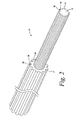
- FIG. 2 is a perspective view of the wire of FIG. 1 with a portion of the insulation removed;
- FIG. 3 is a cross-sectional view of a twisted wire pair according to the embodiment of FIG. 1;
- FIG. 4 is a cross-sectional view of a wire according to another embodiment of the present invention;
- FIG. 5 is a perspective view of the wire of FIG. 4 with a portion of the insulation removed; and
- FIG. 6 is a cross-sectional view of a twisted wire pair according to the embodiment of FIG. 4.
- Turning now to FIG. 1, a cross-sectional view of a
wire 10 is illustrated. The wire includes aconductor 12 and aninsulator 14. Theconductor 12 is non-circular. More specifically, as shown in the embodiment of FIG. 1, the conductor is corrugated, creatingridges 16 anddepressions 17 between theconductor 12 and theinsulator 14. Theridges 16 anddepressions 17 createair gaps 18 that reduce the net dielectric constant of the material between adjacent conductors in a twisted pair. This reduces crosstalk between twisted pairs in a cable comprising multiple twisted pairs. - Corrugating the
conductor 12 also increases the surface area of theconductor 12. Conductors are subject to the skin effect, which means that signals travel at or near the outer peripheral surface of the conductor (according to the electromagnetic field pattern). Increasing the surface area of the conductor increases the area that the signals may travel through without increasing the size of the conductor. Theconductor 12, withair gaps 18 thus has more capacity to transmit data than a smooth conductor having the same size (for mid range frequencies). - The
insulator 14 is also corrugated, havingridges 20 anddepressions 21. Theridges 20 anddepressions 21 also createair gaps 22. Peaks of theridges 20 of theinsulation 14 are aligned with peaks of theridges 16 of theconductor 12 so that theinsulator 14 does not collapse into theair gaps 18 of theconductor 12 when pressure is applied to theinsulator 14. Theridges 20 of theinsulator 14 and theridges 16 of theconductor 12 form a common radius r as shown in FIG. 1. - If pressure is exerted on the
insulator 14, there is risk that theinsulator 14 may collapse into theair gaps 18 of theconductor 12 under pressure. This would cause the dielectric constant to increase, thereby increasing crosstalk and the likelihood of delay skew. Pressure can occur when twowires 10 are being twisted together to create a twisted wire pair. However, with the design shown in FIG. 1, the alignment of theridges 16 of theconductor 12 with theridges 20 of theinsulator 14 keeps theinsulator 14 from collapsing into theair gaps 18. - FIG. 2 illustrates a perspective view of the
wire 10. As seen, theridges depressions conductor 12 andinsulator 14, such that theair gaps ridges - FIG. 3 illustrates a cross-sectional view of a twisted wire pair 30 according to the embodiment of FIG. 1. As shown, when the pairs of
wires 10 are twisted together, theridges 20 of theinsulators 14 may press against each other. However, because peaks of theridges 16 of theconductors 12 are aligned with peaks of theridges 20 of theinsulators 14, neither of theinsulators 14 collapse into theair gaps 18 of theconductors 12. Thus, the overall dielectric constant of the material between theconductors 12 remains low. - Turning now to FIG. 4, another embodiment of the present invention will be described. A
wire 50 is illustrated having anon-circular conductor 52 and aninsulator 54. Theconductor 52 includesridges 56 anddepressions 57, which createsair gaps 58. Theinsulator 54 is a smooth circular surface, with no ridges or depressions. Theair gaps 58 reduce the overall dielectric constant of the material between theconductors 52. - FIG. 5 illustrates a perspective view of the embodiment of FIG. 4. As shown, the
ridges 56 anddepressions 57 extend along the length of the conductor, such that theair gaps 58 create channels. Theridges 56 anddepressions 57 create a sine wave profile, but other shapes and/or curves may be used. Preferably, the shapes have a rounded edge. Also, there may be any number ofridges 56 anddepressions 57. - FIG. 6 illustrates a cross-sectional view of a
twisted wire pair 60 according to the embodiment of FIG. 3. As shown, the pair ofwires 50 are twisted together such that theinsulators 54 abut. Theconductors 52 are corrugated such that theair gaps 58 remain. - While particular embodiments and applications of the present invention have been illustrated and described, it is to be understood that the invention is not limited to the precise construction and compositions disclosed herein and that various modifications, changes, and variations may be apparent from the foregoing descriptions without departing form the spirit and scope of the invention.
- When the dielectric constant is reduced as suggested in this application, the design of the wire pair can be optimized for performance. As the dielectric constant decreases, the capacitance per unit length will decrease proportionally. In order to keep the characteristic impedance constant (i.e., Z0 = SQRT(L/C)), the wire diameters can be increased thus increasing the capacitance per unit length. This increase in the wire diameter will lower the attenuation of the wire pair due to the increase in outer surface area of the wires. On the other hand, if the capacitance is kept smaller due to the decreased dielectric constant, in order to achieve constant characteristic impedance, the inductance must be decreased. With this smaller capacitance and inductance, the characteristic impedance remains constant and the propagation velocity will increase (velocity = 1/(SQRT(LC))).
Claims (12)
- A wire for conducting communication signals, said wire comprising:a corrugated conductor with an outer surface having ridges and depressions thereon, said ridges and depressions having a sine wave profile in cross-section;an insulator surrounding said corrugated conductor; andair gaps between the outer surface of the corrugated conductor and an inner surface of said insulator in regions of said depressions of said conductor.
- The wire of claim 1 wherein said insulator is a corrugated insulator comprising insulator ridges and depressions.
- The wire of claim 2 wherein said insulator ridges are aligned with said ridges of said corrugated conductor.
- A cable for conducting communication signals, said cable being formed of a plurality of wires, at least one of said plurality of wires comprising:a corrugated conductor with an outer surface having ridges and depressions thereon, said ridges and depressions having a sine wave profile in cross-section;an insulator surrounding said corrugated conductor; andair gaps between the outer surface of the corrugated conductor and an inner surface of said insulator in regions of said depressions of said conductor.
- The cable of claim 4 wherein all of said plurality of wires have said corrugated conductors, said insulators surrounding said corrugated conductors, and said air gaps.
- The cable of claim 5 wherein said insulator is a corrugated insulator comprising insulator ridges and depressions.
- The cable of claim 6 wherein said insulator ridges are aligned with said ridges of said corrugated conductor.
- The cable of claim 4 wherein said plurality of wires are arranged as twisted wire pairs.
- A wire for conducting communication signals, said wire comprising:a corrugated conductor with an outer surface having conductor ridges and depressions thereon, each of said conductor ridges having a peak; anda corrugated insulator surrounding said corrugated conductor, said corrugated insulator having insulator ridges and depressions thereon, each of said insulator ridges having a peak; wherein
said peaks of said conductor ridges are aligned with said peaks of said insulator ridges. - The wire of claim 9 wherein said conductor ridges and depressions have a sine wave profile in cross-section.
- The wire of claim 9 wherein said insulator ridges and depressions have a sine wave profile in cross-section.
- The wire of claim 9 wherein said conductor ridges have rounded edges.
Applications Claiming Priority (2)
| Application Number | Priority Date | Filing Date | Title |
|---|---|---|---|
| US80363906P | 2006-06-01 | 2006-06-01 | |
| US11/755,090 US7601916B2 (en) | 2006-06-01 | 2007-05-30 | Conductor with non-circular cross-section |
Publications (2)
| Publication Number | Publication Date |
|---|---|
| EP1863039A2 true EP1863039A2 (en) | 2007-12-05 |
| EP1863039A3 EP1863039A3 (en) | 2012-07-18 |
Family
ID=38460596
Family Applications (1)
| Application Number | Title | Priority Date | Filing Date |
|---|---|---|---|
| EP07252241A Withdrawn EP1863039A3 (en) | 2006-06-01 | 2007-06-01 | Conductor with non-circular cross-section |
Country Status (4)
| Country | Link |
|---|---|
| US (1) | US7601916B2 (en) |
| EP (1) | EP1863039A3 (en) |
| JP (1) | JP2008004542A (en) |
| KR (1) | KR20070115767A (en) |
Cited By (4)
| Publication number | Priority date | Publication date | Assignee | Title |
|---|---|---|---|---|
| WO2009087662A3 (en) * | 2008-01-07 | 2009-09-11 | Narendra Prabhakar Bonde | Super- conducting electrical conductor with low resistance at ambient temperature |
| CN102129894B (en) * | 2010-01-20 | 2012-07-11 | 刘理文 | High-conductivity energy-saving cable and manufacturing method thereof |
| WO2013018922A1 (en) * | 2011-08-02 | 2013-02-07 | Yazaki Corporation | Terminal crimping structure for single core electric wire |
| WO2014154786A1 (en) * | 2013-03-28 | 2014-10-02 | Alstom Technology Ltd | Self-deicing lightweight conductor |
Families Citing this family (9)
| Publication number | Priority date | Publication date | Assignee | Title |
|---|---|---|---|---|
| US7479597B1 (en) * | 2007-11-28 | 2009-01-20 | International Business Machines Corporation | Conductor cable having a high surface area |
| JP5362226B2 (en) * | 2008-01-17 | 2013-12-11 | 矢崎総業株式会社 | Electrical wire |
| US20090233052A1 (en) * | 2008-03-17 | 2009-09-17 | E.I. Du Pont De Nemours And Company | Conductors Having Polymer Insulation On Irregular Surface |
| TWI391668B (en) * | 2008-11-21 | 2013-04-01 | 京元電子股份有限公司 | Electrical connection conductor with high current withstand capability and method for improving current withstand capability of electrical connection conductor |
| WO2011021999A1 (en) * | 2009-08-18 | 2011-02-24 | Halliburton Energy Services | Smooth wireline |
| JP5645129B2 (en) * | 2011-04-01 | 2014-12-24 | 日立金属株式会社 | High frequency coaxial cable and manufacturing method thereof |
| US20140119699A1 (en) * | 2012-10-25 | 2014-05-01 | Nexans | Optical fiber cable having spline profiled insulation |
| US10312000B2 (en) | 2016-07-07 | 2019-06-04 | Nexans | Heat dissipating cable jacket |
| US10535449B2 (en) * | 2018-01-29 | 2020-01-14 | Sterlite Technologies Limited | Notched conductor for telecommunication |
Family Cites Families (7)
| Publication number | Priority date | Publication date | Assignee | Title |
|---|---|---|---|---|
| JPH02223104A (en) * | 1988-11-30 | 1990-09-05 | Toshiba Corp | Copper-group member and manufacture thereof |
| GB9416331D0 (en) * | 1994-08-12 | 1994-10-05 | Amp Gmbh | Stranded electrical wire for use with IDC |
| DE19519582A1 (en) * | 1995-05-29 | 1996-12-12 | Daetwyler Ag | Conductor cores for HF electric cables with reduced skin effect |
| US5990419A (en) * | 1996-08-26 | 1999-11-23 | Virginia Patent Development Corporation | Data cable |
| JP2003272446A (en) | 2002-03-19 | 2003-09-26 | Goto Denshi Kk | Electric wire |
| US7214880B2 (en) * | 2002-09-24 | 2007-05-08 | Adc Incorporated | Communication wire |
| US20040256139A1 (en) * | 2003-06-19 | 2004-12-23 | Clark William T. | Electrical cable comprising geometrically optimized conductors |
-
2007
- 2007-05-30 US US11/755,090 patent/US7601916B2/en not_active Expired - Fee Related
- 2007-05-31 JP JP2007145065A patent/JP2008004542A/en not_active Withdrawn
- 2007-06-01 KR KR1020070053647A patent/KR20070115767A/en not_active Withdrawn
- 2007-06-01 EP EP07252241A patent/EP1863039A3/en not_active Withdrawn
Cited By (6)
| Publication number | Priority date | Publication date | Assignee | Title |
|---|---|---|---|---|
| WO2009087662A3 (en) * | 2008-01-07 | 2009-09-11 | Narendra Prabhakar Bonde | Super- conducting electrical conductor with low resistance at ambient temperature |
| CN102129894B (en) * | 2010-01-20 | 2012-07-11 | 刘理文 | High-conductivity energy-saving cable and manufacturing method thereof |
| WO2013018922A1 (en) * | 2011-08-02 | 2013-02-07 | Yazaki Corporation | Terminal crimping structure for single core electric wire |
| WO2014154786A1 (en) * | 2013-03-28 | 2014-10-02 | Alstom Technology Ltd | Self-deicing lightweight conductor |
| FR3003992A1 (en) * | 2013-03-28 | 2014-10-03 | Alstom Technology Ltd | AUTO LIGHTWEIGHT DEPLACANT DRIVER |
| US9941080B2 (en) | 2013-03-28 | 2018-04-10 | Alstom Technology Ltd | Self-deicing lightweight conductor |
Also Published As
| Publication number | Publication date |
|---|---|
| JP2008004542A (en) | 2008-01-10 |
| EP1863039A3 (en) | 2012-07-18 |
| KR20070115767A (en) | 2007-12-06 |
| US7601916B2 (en) | 2009-10-13 |
| US20070277996A1 (en) | 2007-12-06 |
Similar Documents
| Publication | Publication Date | Title |
|---|---|---|
| US7601916B2 (en) | Conductor with non-circular cross-section | |
| US7772494B2 (en) | Web for separating conductors in a communication cable | |
| EP2592631B1 (en) | Discontinous cable shield system | |
| JP5141660B2 (en) | Differential signal cable, transmission cable using the same, and method for manufacturing differential signal cable | |
| JP5454648B2 (en) | Differential signal cable, transmission cable using the same, and method for manufacturing differential signal cable | |
| US6787694B1 (en) | Twisted pair cable with dual layer insulation having improved transmission characteristics | |
| US10134507B2 (en) | Cable having improved anti cross talk performance | |
| CN104008815B (en) | Discontinuous shielding band for communication cable | |
| JP5669033B2 (en) | Differential signal cable, transmission cable using the same, and direct attach cable | |
| US20060180329A1 (en) | Enhanced communication cable systems and methods | |
| US20250273365A1 (en) | Shield-supporting filler for data communications cables with reduced cross-sectional diameter | |
| US10079082B2 (en) | Data transmission cable | |
| JP5347166B2 (en) | Invention of balanced cable for LAN extending maximum link length in LAN wiring system | |
| US20190043641A1 (en) | Data transmission cable | |
| KR101387241B1 (en) | Data cable for high speed communication except for cross-filler | |
| CN101083160A (en) | Conductor with non-circular cross-section | |
| KR20150021181A (en) | Communication cable comprising discontinuous shield tape and discontinuous shield tape | |
| KR101160160B1 (en) | Utp cable for high speed communication | |
| JP3547164B2 (en) | communication cable | |
| HK1179746A (en) | Discontinous cable shield system | |
| JP2004063134A (en) | Connection method and connection structure of collective cable | |
| KR20000047369A (en) | Twisted twin cable and Jumper with bonding parts of insulation layer |
Legal Events
| Date | Code | Title | Description |
|---|---|---|---|
| PUAI | Public reference made under article 153(3) epc to a published international application that has entered the european phase |
Free format text: ORIGINAL CODE: 0009012 |
|
| AK | Designated contracting states |
Kind code of ref document: A2 Designated state(s): AT BE BG CH CY CZ DE DK EE ES FI FR GB GR HU IE IS IT LI LT LU LV MC MT NL PL PT RO SE SI SK TR |
|
| AX | Request for extension of the european patent |
Extension state: AL BA HR MK YU |
|
| PUAL | Search report despatched |
Free format text: ORIGINAL CODE: 0009013 |
|
| AK | Designated contracting states |
Kind code of ref document: A3 Designated state(s): AT BE BG CH CY CZ DE DK EE ES FI FR GB GR HU IE IS IT LI LT LU LV MC MT NL PL PT RO SE SI SK TR |
|
| AX | Request for extension of the european patent |
Extension state: AL BA HR MK RS |
|
| RIC1 | Information provided on ipc code assigned before grant |
Ipc: H01B 7/02 20060101AFI20120611BHEP |
|
| AKY | No designation fees paid | ||
| REG | Reference to a national code |
Ref country code: DE Ref legal event code: R108 |
|
| REG | Reference to a national code |
Ref country code: DE Ref legal event code: R108 Effective date: 20130327 |
|
| STAA | Information on the status of an ep patent application or granted ep patent |
Free format text: STATUS: THE APPLICATION IS DEEMED TO BE WITHDRAWN |
|
| 18D | Application deemed to be withdrawn |
Effective date: 20130103 |