EP1860775A1 - Driving configuration of a switch - Google Patents
Driving configuration of a switch Download PDFInfo
- Publication number
- EP1860775A1 EP1860775A1 EP06425359A EP06425359A EP1860775A1 EP 1860775 A1 EP1860775 A1 EP 1860775A1 EP 06425359 A EP06425359 A EP 06425359A EP 06425359 A EP06425359 A EP 06425359A EP 1860775 A1 EP1860775 A1 EP 1860775A1
- Authority
- EP
- European Patent Office
- Prior art keywords
- switch
- driving
- terminal
- transistors
- driving device
- Prior art date
- Legal status (The legal status is an assumption and is not a legal conclusion. Google has not performed a legal analysis and makes no representation as to the accuracy of the status listed.)
- Withdrawn
Links
- 239000003990 capacitor Substances 0.000 claims description 14
- 238000006243 chemical reaction Methods 0.000 claims description 4
- 238000004088 simulation Methods 0.000 description 5
- 244000045947 parasite Species 0.000 description 3
- 230000001052 transient effect Effects 0.000 description 3
- 238000004513 sizing Methods 0.000 description 2
- 239000011800 void material Substances 0.000 description 2
- 238000012423 maintenance Methods 0.000 description 1
- 239000000758 substrate Substances 0.000 description 1
Images


Classifications
-
- H—ELECTRICITY
- H03—ELECTRONIC CIRCUITRY
- H03K—PULSE TECHNIQUE
- H03K17/00—Electronic switching or gating, i.e. not by contact-making and –breaking
- H03K17/51—Electronic switching or gating, i.e. not by contact-making and –breaking characterised by the components used
- H03K17/56—Electronic switching or gating, i.e. not by contact-making and –breaking characterised by the components used by the use, as active elements, of semiconductor devices
- H03K17/687—Electronic switching or gating, i.e. not by contact-making and –breaking characterised by the components used by the use, as active elements, of semiconductor devices the devices being field-effect transistors
- H03K17/6871—Electronic switching or gating, i.e. not by contact-making and –breaking characterised by the components used by the use, as active elements, of semiconductor devices the devices being field-effect transistors the output circuit comprising more than one controlled field-effect transistor
- H03K17/6874—Electronic switching or gating, i.e. not by contact-making and –breaking characterised by the components used by the use, as active elements, of semiconductor devices the devices being field-effect transistors the output circuit comprising more than one controlled field-effect transistor in a symmetrical configuration
-
- H—ELECTRICITY
- H03—ELECTRONIC CIRCUITRY
- H03K—PULSE TECHNIQUE
- H03K17/00—Electronic switching or gating, i.e. not by contact-making and –breaking
- H03K17/04—Modifications for accelerating switching
- H03K17/042—Modifications for accelerating switching by feedback from the output circuit to the control circuit
- H03K17/04206—Modifications for accelerating switching by feedback from the output circuit to the control circuit in field-effect transistor switches
Definitions
- the present invention relates to a driving configuration of a switch.
- the invention relates to a driving configuration of a switch realised by means of a first and a second transistor connected in series to each other and to the relative intrinsic diodes in antiseries and driven by a driving device.
- the invention particularly, but not exclusively, relates to a driving configuration of a high voltage (HV) switch and the following description is made with reference to this field of application by way of illustration only.
- HV high voltage
- a driving device of a high voltage (HV) switch is requested to instantaneously follow the voltage dynamics of a signal to be switched.
- a switch realised by means of a high voltage MOD or DMOS transistor is able to manage high voltages between its drain and source terminals, as well as with respect to a substrate potential.
- the highest voltage value Vgs between its gate and source terminals is however limited to some volts (3V or 5V).
- the switch when the switch is off it must be able to interrupt the passage of current independently from the voltage polarity at its ends. Further to the connection of the body terminal to the source terminal, a junction is created between the source and drain terminals, which prevents the inversion of the polarity across the switch without triggering a passage of current in the intrinsic diode thus created even if the relative channel is off.
- the switch is realised by placing two MOS or DMOS transistors in series, so that the relative intrinsic diodes are biased in antiseries, i.e. with a pair of corresponding terminals, in particular respective anodes, in common. In this way, at least one intrinsic diode of the switch is always inversely biased.
- a driving device or driver is to be provided able to follow a turn on/off command of the switch and to apply a first turn on voltage value (for example equal to 5V) between the gate and source terminals of the transistors contained in the switch when the switch itself is to be turned on and a second turn off voltage value (for example equal to 0V) between the gate and source terminals of the transistors contained in the switch when it is to be turned off.
- a first turn on voltage value for example equal to 5V
- a second turn off voltage value for example equal to 0V
- a configuration 5 of driven switch comprising a switch 1 realised by means of two DMOS transistors, DM1, DM2, connected in series, with intrinsic diodes in antiseries and driven by means of a driving device or driver 2 is schematically shown in Figure 1.
- this configuration 5 comprises a resistive element Rgs which connects respective common source SS and gate GG terminals of the DM1 and DM2 transistors of the switch 1.
- the DM1 and DM2 transistors also have respective drain terminals, D1 and D2.
- the driver 2 is inserted between a first and a second voltage reference, respectively a supply Vss (for example equal to 3.3V) and a ground GND (for example equal to OV), and it has an input terminal IN receiving a driving signal Sin for driving the switch 1 in a first on state (ON) and in a second off state (OFF).
- the driving signal Sin is a digital signal having a first level or 0 logic corresponding to a demand for turn on of the switch 1 and a second level or 1 logic corresponding to a demand for turn off of the switch 1.
- the driver 2 also has an output terminal, OUT, connected, by means of a level shifter 3 to the gate terminals GG of the switch 1. On the output terminal OUT of the driver 2 there is a control signal Sc for the switch 1, derived from the driving signal Sin applied to its input terminal IN
- the voltage value at the drain and source terminals of the transistors comprised in the switch 1 must take all the values between a negative - HV and a positive +HV high voltage reference, for example equal to 100V and a level shifter 3 is thus to be used, the shifter being able to shift a control signal Sc referred to the ground GND and to refer it to an instantaneous level of a signal Scomm to be switched and applied to a terminal of the switch 1, in particular to the D 1 and D2 drain terminals.
- the level shifter 3 is realised in a simple and functional way so as to convert the control signal Sc in voltage (referred to the GND) into a control signal in current and then again into a control signal Scd derived in voltage referred to the common source terminals SS of the DM 1 and DM2 transistors comprised in the switch 1.
- the level shifter 3 comprises a first transistor M1 having a control or gate terminal connected to the output terminal OUT of the driver 2, a first conduction terminal, in particular a source terminal, connected, by means of the parallel of a current generator CSG (in particular a low voltage one) and of a capacitor Cff (so called feed forward capacitor), to the GND, as well as a second conduction terminal, in particular a drain terminal, connected to a shifted voltage reference VPP (equal to a high voltage value, for example +3V) by means of a current mirror realised by a second M2 and a third M3 transistor.
- the second transistor M2 is inserted between the shifted voltage reference VPP and the drain terminal of the first transistor M1, it is diode-wise configured and it has a gate terminal connected to the gate terminal of the third transistor M3, in turn inserted between the shifted voltage reference VPP and an output terminal OUT* of the level shifter 3, in turn connected to the gate terminals GG of the switch 1.
- this known configuration shows a serious drawback linked to the sizing of the resistive element Rgs inserted between the common gate GG and the source SS terminals of the DM 1 and DM2 transistors of the switch 1.
- the configuration 5 shown in Figure 1 must use a variable resistance being small when the switch 1 is off and high when it is on.
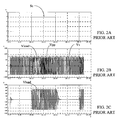
- Figure 2B shows the supply voltage signal Vpp, the source voltage signal Vs and the voltage signal which is obtained on the load Vload, overlapped onto each other, while Figure 2C reports the signal on the load Vload only.
- the switch 1 works correctly and reports the source voltage value Vs on the load (Vload signal overlapped onto Vs in Figure 2B) as soon as the control signal Sc is brought to Vpp (turn on of the switch 1).
- This switch 1 does not however work correctly during the turn off (Sc is brought back to 0) since the voltage signal on the load Vload dampens only gradually starting from 20 microseconds (time in which the control signal Sc is interrupted in Figure 2C), the turn off being relied only upon the resistive element Rgs. From these results, it is immediate to verify how such a value of the resistive element Rgs thus implies a long turn off time of the switch 1.
- the technical problem underlying the present invention is that of providing a driving configuration of a high voltage switch able to associate, with a quick switch transient, a reasonable control current value, overcoming in this way the limits and drawbacks still affecting the configurations realised according to the prior art.
- the solution idea underlying the present invention is that of introducing, between the gate and source terminals of a switch driven by a driver, a latch circuit able to realise a correct connection of these gate terminals to suitable current values according to the working conditions of the switch itself, in particular during the turn on and off.
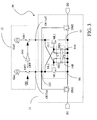
- a driving configuration of a switch in particular a high voltage one being driven by a driving device or driver is globally and schematically indicated with 10.
- the driving configuration 10 comprises a switch 11 realised by means of first and second transistors, DM1 and DM2, in particular MOS or DMOS transistors, connected, in series to each other and to relative intrinsic diodes in antiseries, i.e. to a pair of corresponding terminals, in particular anodes, in common.
- the switch 11 is driven by a driving device or driver 12 having first OUToff and second OUTon output terminals connected to the switch 11.
- the driver 12 essentially comprises first Goff and second Gon control current generators, connected, by means of respective first SW1 and second SW2 driven switches, to the first OUToff and second OUTon output terminals of the driver 12 itself.
- the first switch SW2 is driven, by means of an inverter INV, by a first turn off command OFF, while the second switch SW2 is driven by a second turn on command ON.
- the driving configuration 10 further comprises a latch circuit 13 inserted between common respective source SS and gate GG terminals of the DM1 and DM2 transistors of the switch 11.
- the latch circuit 13 comprises at least one first ML1 and one second ML2 latch transistor inserted between the source SS and gate GG terminals connected in positive reaction to each other, i.e. in latch configuration (more exactly, a semi-latch one).
- the first latch transistor ML1 is inserted between the first output terminal OUToff of the driver 12 and the source terminal SS and it has a control or gate terminal GL1 connected to the gate terminal GG;
- the second latch transistor ML2 is inserted between the second output terminal OUTon of the driver 12, in turn connected to the gate terminal GG, and the source terminal SS and it has a control or gate terminal GL2 connected to the first output terminal OUToff of the driver 12.
- the latch circuit 13 further comprises a first Zener diode DZ1 and a first capacitor C1 inserted, in parallel to each other, between the gate terminal GL1 of the first latch transistor ML1 and the source terminal SS, as well as a second Zener diode DZ2 and a second capacitor C2 inserted, in parallel to each other, between the gate terminal GL2 of the second latch transistor ML2 and the source terminal SS.
- the latch circuit 13 performs the functions of the resistive element Rgs connected between the gate GG and source SS terminals of the driving configuration according to the prior art, ensuring a correct connection of the gate terminals GG to suitable current values supplied by the driver 12 according to the working conditions of the driving configuration 10, i.e. when the switch 11 is driven to the turn off, respectively to the turn on.
- the latch transistors, ML1 and ML2, in the configuration provided for the latch circuit 13, work so as to turn off each other according to the working condition of the switch 11.
- These latch transistors are in particular N channel MOS transistors with low voltage (in particular, equal to 5V).
- the turn on of the first latch transistor ML1 causes the turn off of the second latch transistor ML2, since it nullifies its voltage value Vgs between the gate and source terminals, which are short-circuited to each other.
- the turn on of the second latch transistor ML2 causes the turn off of the first latch transistor ML1, nullifying the voltage value Vgs between the gate and source terminals.
- the value of the current injected by the control current generators, Goff and Gon, of the driver 12 closes itself on an infinite impedance (corresponding to the latch transistor when off) and thus, with a few ⁇ A of supplied current the driving configuration 10 according to the invention is able to develop a voltage value sufficient to ensure a correct turn on, respectively turn off, of the switch 11.
- the value of the voltage produced by the latch circuit 13 on the gate terminal of the latch transistor when on is clamped thanks to the diodes Zener, DZ1 and DZ2, and to the capacitors, C1 and C2, connected between this gate terminal and the source terminal SS.
- the Zener diode DZ1 and the capacitor C1 connected to the gate terminal GL1 of the first latch transistor ML1 realise a clamp circuit 14A of a value of the current being on this gate terminal GL1.
- the Zener diode DZ2 and the capacitor C2 connected to the gate terminal GL2 of the second latch transistor ML2 realise a further clamp circuit 14B of a voltage value being on this gate terminal GL2.
- the capacitors, C1 and C2, connected to the gate terminals, GL1 and GL2, of the latch transistors, ML1 and ML2, are advantageously sized so as to result dominant with respect to parasite capacities of these gate terminals, ensuring in this way the maintenance of an ON or OFF state in the absence of a control signal.
- Simulations carried out by the Applicant on the driving configuration 10 shown in Figure 3 have shown switch times from an OFF state to an ON state substantially identical to those form the ON state to the OFF state and in the order of 200ns.
- Figures 5A-5C The results of these simulations are shown in Figures 5A-5C in the case in which the switch 11 connects a load to a voltage signal source Vs.
- Figure 5B shows the source voltage signal Vs and the voltage signal which is obtained on the load Vload, overlapped onto each other while Figure 5C reports the signal on the load Vload only.
- the driving configuration 10 allows to meet the demands for a quick switch transient for a switch driven in high voltage, although preserving an unusual implementing simplicity.
- Such a driving configuration however shows a considerable power dissipation, essentially due to the continuous charge/discharge of the capacitors, C1 and C2, connected to the gate terminals, GL1 and GL2, of the latch transistors, ML1 and ML2, of the latch circuit 13.
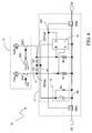
- the driving configuration 10 comprises a switch 11 driven by a driver 12 and comprises a latch circuit 15 inserted between the gate GG and source SS terminals of the transistors, DM1 and DM2, of the switch 11.
- the latch circuit 15 comprises a digital latch or flip-flop 16 of the Set/Reset type, usually realised with two logic gates of the NOR type.
- the flip-flop 16 allows a switch from an ON state to an OFF state simply by means of SET and RESET signals received as voltage signals across respective set Rs, and reset, Rr, resistances, suitably connected to the set S and reset R terminals of the flip-flop 16.
- the flip-flop 16 is inserted between an inner circuit node Xc and the source terminal SS and it has:
- the latch circuit 15 comprises a Zener diode DZ and a capacitor C inserted, in parallel to each other, between the inner circuit node Xc and the source terminal SS. Also in this case, the Zener diode DZ and the capacitor C realise a clamp circuit 18 of the supply voltage value being on the inner circuit node Xc.
- the value of the current injected onto the set and reset resistances, Rs and Rr, by the driver 12 must not close itself on variable and not known channel resistances.
- the proposed driving configuration 10 is supplied with a supply voltage corresponding to the one necessary for the correct working of its components, in particular those used for realising the NOR gates of the flip-flop 16.
- the driving configuration 10 comprises a rectifier 17, inserted between the output terminals, OUToff and OUTon, of the driver 12 and the supply inner circuit node Xc of the flip-flop 16.
- the rectifier 17 comprises a first D1 and a second diode D2 connected, in counter-series to each other, between these output terminals, OUToff and OUTon, and interconnected in correspondence with the inner circuit node Xc.
- a supply voltage value for the flip-flop 16 is taken by rectifying a charge value of parasite capacities associated with the control current generators, Goff and Gon, comprised in the driver 12, this supply value being always refreshed at each switch carried out by the switch 11.
- the capacitor C of the clamp circuit 18 is not continuously loaded and unloaded, but its energy is preserved for ensuring the state of the switch 11 for long times.
- the driving configuration 10 described with reference to Figure 4 allows to realise the driving for a high voltage switch able to associate, with the characteristic of low consume, a quick switch transient.
Landscapes
- Electronic Switches (AREA)
- Power Conversion In General (AREA)
Abstract
A driving configuration (10) of a switch (11) is described, this latter being realised by means of first and second transistors (DM1, DM2) connected, in series to each other and to relative intrinsic diodes in antiseries, and driven by a driving device (12). Advantageously, the driving device (12) comprises at least one first and one second output terminal (OUToff, OUTon) connected to the switch (11) and suitable to supply it with a first control signal (Goff) for driving the switch (11) in a first working state (OFF) and a second control signal (Gon) for driving the switch (11) in a second working state (ON). The driving configuration (10) suitably comprises at least one latch circuit (13, 15) inserted between respective common gate and source terminals (GG, SS) of the first and second transistors (DM1, DM2) and suitable to supply the common gate terminal (GG) with the first and second control signals (Goff, Gon), respectively, according to the working state (OFF, ON) for the turn off, respectively the turn on, of the first and second transistors (DM1, DM2).
Description
- The present invention relates to a driving configuration of a switch.
- More specifically, the invention relates to a driving configuration of a switch realised by means of a first and a second transistor connected in series to each other and to the relative intrinsic diodes in antiseries and driven by a driving device.
- The invention particularly, but not exclusively, relates to a driving configuration of a high voltage (HV) switch and the following description is made with reference to this field of application by way of illustration only.
- As it is well known, a driving device of a high voltage (HV) switch, usually realised by means of a MOS transistor, is requested to instantaneously follow the voltage dynamics of a signal to be switched.
- In general, a switch realised by means of a high voltage MOD or DMOS transistor is able to manage high voltages between its drain and source terminals, as well as with respect to a substrate potential. The highest voltage value Vgs between its gate and source terminals is however limited to some volts (3V or 5V).
- In particular, when the switch is off it must be able to interrupt the passage of current independently from the voltage polarity at its ends. Further to the connection of the body terminal to the source terminal, a junction is created between the source and drain terminals, which prevents the inversion of the polarity across the switch without triggering a passage of current in the intrinsic diode thus created even if the relative channel is off.
- To overcome this drawback, the switch is realised by placing two MOS or DMOS transistors in series, so that the relative intrinsic diodes are biased in antiseries, i.e. with a pair of corresponding terminals, in particular respective anodes, in common. In this way, at least one intrinsic diode of the switch is always inversely biased.
- In this case a driving device or driver is to be provided able to follow a turn on/off command of the switch and to apply a first turn on voltage value (for example equal to 5V) between the gate and source terminals of the transistors contained in the switch when the switch itself is to be turned on and a second turn off voltage value (for example equal to 0V) between the gate and source terminals of the transistors contained in the switch when it is to be turned off.
- A
configuration 5 of driven switch comprising aswitch 1 realised by means of two DMOS transistors, DM1, DM2, connected in series, with intrinsic diodes in antiseries and driven by means of a driving device ordriver 2 is schematically shown in Figure 1. - In particular, this
configuration 5 comprises a resistive element Rgs which connects respective common source SS and gate GG terminals of the DM1 and DM2 transistors of theswitch 1. The DM1 and DM2 transistors also have respective drain terminals, D1 and D2. - The
driver 2 is inserted between a first and a second voltage reference, respectively a supply Vss (for example equal to 3.3V) and a ground GND (for example equal to OV), and it has an input terminal IN receiving a driving signal Sin for driving theswitch 1 in a first on state (ON) and in a second off state (OFF). In particular, the driving signal Sin is a digital signal having a first level or 0 logic corresponding to a demand for turn on of theswitch 1 and a second level or 1 logic corresponding to a demand for turn off of theswitch 1. - The
driver 2 also has an output terminal, OUT, connected, by means of alevel shifter 3 to the gate terminals GG of theswitch 1. On the output terminal OUT of thedriver 2 there is a control signal Sc for theswitch 1, derived from the driving signal Sin applied to its input terminal IN - In fact, it is to be underlined that, in high voltage applications, the voltage value at the drain and source terminals of the transistors comprised in the
switch 1 must take all the values between a negative - HV and a positive +HV high voltage reference, for example equal to 100V and alevel shifter 3 is thus to be used, the shifter being able to shift a control signal Sc referred to the ground GND and to refer it to an instantaneous level of a signal Scomm to be switched and applied to a terminal of theswitch 1, in particular to theD 1 and D2 drain terminals. - As shown in Figure 1, the
level shifter 3 is realised in a simple and functional way so as to convert the control signal Sc in voltage (referred to the GND) into a control signal in current and then again into a control signal Scd derived in voltage referred to the common source terminals SS of theDM 1 and DM2 transistors comprised in theswitch 1. - For realising this conversion, the
level shifter 3 comprises a first transistor M1 having a control or gate terminal connected to the output terminal OUT of thedriver 2, a first conduction terminal, in particular a source terminal, connected, by means of the parallel of a current generator CSG (in particular a low voltage one) and of a capacitor Cff (so called feed forward capacitor), to the GND, as well as a second conduction terminal, in particular a drain terminal, connected to a shifted voltage reference VPP (equal to a high voltage value, for example +3V) by means of a current mirror realised by a second M2 and a third M3 transistor. - In particular, the second transistor M2 is inserted between the shifted voltage reference VPP and the drain terminal of the first transistor M1, it is diode-wise configured and it has a gate terminal connected to the gate terminal of the third transistor M3, in turn inserted between the shifted voltage reference VPP and an output terminal OUT* of the
level shifter 3, in turn connected to the gate terminals GG of theswitch 1. - Although advantageous under several aspects, this known configuration shows a serious drawback linked to the sizing of the resistive element Rgs inserted between the common gate GG and the source SS terminals of the
DM 1 and DM2 transistors of theswitch 1. - In fact, if the
switch 1 is to be switched quickly this resistive element Rgs is to be sized with a relatively small value, so that the time constant τ given by the resistive element Rgs itself and by the parasite capacities Cpar associated with the gate nodes is brief and smaller than a switch time Tcomm (in this case, a turn off time) desired. In particular, it results
- Thus, by using a small resistance value for the resistive element Rgs so as to meet the above reported relation (1), a high current value Ion is however to be provided during the turn on, this current value having in fact to meet, for the voltage between the gate and source terminals of the
DM 1 and DM2 transistors, the following relation:
- In other words, the
configuration 5 shown in Figure 1 must use a variable resistance being small when theswitch 1 is off and high when it is on. - Such a
configuration 5, using a resistive element Rgs of 500kOhm, has been simulated by the Applicant in the case in which theswitch 1 connects a load to a source of a voltage signal Vs. The results of this simulation being shown in Figures 2A, 2B and 2C. In particular, Figure 2A shows a control signal Sc of theswitch 1, for which a void voltage value (Sc=0) corresponds to a condition of open switch, and a voltage value equal to Vpp (Sc=5V) corresponds to a condition of closed switch. Figure 2B shows the supply voltage signal Vpp, the source voltage signal Vs and the voltage signal which is obtained on the load Vload, overlapped onto each other, while Figure 2C reports the signal on the load Vload only. Thus, theswitch 1 works correctly and reports the source voltage value Vs on the load (Vload signal overlapped onto Vs in Figure 2B) as soon as the control signal Sc is brought to Vpp (turn on of the switch 1). Thisswitch 1 does not however work correctly during the turn off (Sc is brought back to 0) since the voltage signal on the load Vload dampens only gradually starting from 20 microseconds (time in which the control signal Sc is interrupted in Figure 2C), the turn off being relied only upon the resistive element Rgs. From these results, it is immediate to verify how such a value of the resistive element Rgs thus implies a long turn off time of theswitch 1. - The technical problem underlying the present invention is that of providing a driving configuration of a high voltage switch able to associate, with a quick switch transient, a reasonable control current value, overcoming in this way the limits and drawbacks still affecting the configurations realised according to the prior art.
- The solution idea underlying the present invention is that of introducing, between the gate and source terminals of a switch driven by a driver, a latch circuit able to realise a correct connection of these gate terminals to suitable current values according to the working conditions of the switch itself, in particular during the turn on and off.
- On the basis of this solution idea the technical problem is solved by a driving configuration as previously indicated and defined by the characterising part of
claim 1. - The characteristics and the advantages of the driving configuration according to the invention will be apparent from the following description of an embodiment thereof given by way of indicative and non limiting example with reference to the annexed drawings.
- In these drawings:
- Figure 1 schematically shows a driving configuration of a high voltage switch realised according to the prior art;
- Figures 2A-2C show the results of a simulation carried out on the driving configuration of Figure 1;
- Figure 3 schematically shows a driving configuration realised according to the invention;
- Figure 4 schematically shows a further embodiment of the driving configuration according to the invention; and
- Figures 5A-5C show the results of a simulation carried out on the driving configuration of Figure 3.
- With reference to these figures, and in particular to Figure 3, a driving configuration of a switch, in particular a high voltage one being driven by a driving device or driver is globally and schematically indicated with 10.
- Elements being structurally and functionally corresponding to the driving configuration described in relation to the prior art and shown in Figure 1 will be given the same reference numbers by way of illustration.
- In particular, the
driving configuration 10 comprises aswitch 11 realised by means of first and second transistors, DM1 and DM2, in particular MOS or DMOS transistors, connected, in series to each other and to relative intrinsic diodes in antiseries, i.e. to a pair of corresponding terminals, in particular anodes, in common. - The
switch 11 is driven by a driving device ordriver 12 having first OUToff and second OUTon output terminals connected to theswitch 11. - The
driver 12 essentially comprises first Goff and second Gon control current generators, connected, by means of respective first SW1 and second SW2 driven switches, to the first OUToff and second OUTon output terminals of thedriver 12 itself. In particular, the first switch SW2 is driven, by means of an inverter INV, by a first turn off command OFF, while the second switch SW2 is driven by a second turn on command ON. - Advantageously according to the invention, the
driving configuration 10 further comprises alatch circuit 13 inserted between common respective source SS and gate GG terminals of the DM1 and DM2 transistors of theswitch 11. - The
latch circuit 13 comprises at least one first ML1 and one second ML2 latch transistor inserted between the source SS and gate GG terminals connected in positive reaction to each other, i.e. in latch configuration (more exactly, a semi-latch one). In particular, the first latch transistor ML1 is inserted between the first output terminal OUToff of thedriver 12 and the source terminal SS and it has a control or gate terminal GL1 connected to the gate terminal GG; similarly, the second latch transistor ML2 is inserted between the second output terminal OUTon of thedriver 12, in turn connected to the gate terminal GG, and the source terminal SS and it has a control or gate terminal GL2 connected to the first output terminal OUToff of thedriver 12. - The
latch circuit 13 further comprises a first Zener diode DZ1 and a first capacitor C1 inserted, in parallel to each other, between the gate terminal GL1 of the first latch transistor ML1 and the source terminal SS, as well as a second Zener diode DZ2 and a second capacitor C2 inserted, in parallel to each other, between the gate terminal GL2 of the second latch transistor ML2 and the source terminal SS. - In this way, advantageously according to the invention, the
latch circuit 13 performs the functions of the resistive element Rgs connected between the gate GG and source SS terminals of the driving configuration according to the prior art, ensuring a correct connection of the gate terminals GG to suitable current values supplied by thedriver 12 according to the working conditions of thedriving configuration 10, i.e. when theswitch 11 is driven to the turn off, respectively to the turn on. - In fact, the latch transistors, ML1 and ML2, in the configuration provided for the
latch circuit 13, work so as to turn off each other according to the working condition of theswitch 11. These latch transistors are in particular N channel MOS transistors with low voltage (in particular, equal to 5V). - It is in fact evident that, thanks to the crossed connection of the gate and drain terminals of the latch transistors, ML1 and ML2, the turn on of the first latch transistor ML1 causes the turn off of the second latch transistor ML2, since it nullifies its voltage value Vgs between the gate and source terminals, which are short-circuited to each other. Similarly, the turn on of the second latch transistor ML2 causes the turn off of the first latch transistor ML1, nullifying the voltage value Vgs between the gate and source terminals.
- In this way, the value of the current injected by the control current generators, Goff and Gon, of the
driver 12 closes itself on an infinite impedance (corresponding to the latch transistor when off) and thus, with a few µA of supplied current thedriving configuration 10 according to the invention is able to develop a voltage value sufficient to ensure a correct turn on, respectively turn off, of theswitch 11. The value of the voltage produced by thelatch circuit 13 on the gate terminal of the latch transistor when on is clamped thanks to the diodes Zener, DZ1 and DZ2, and to the capacitors, C1 and C2, connected between this gate terminal and the source terminal SS. - In other words, the Zener diode DZ1 and the capacitor C1 connected to the gate terminal GL1 of the first latch transistor ML1 realise a
clamp circuit 14A of a value of the current being on this gate terminal GL1. Similarly, the Zener diode DZ2 and the capacitor C2 connected to the gate terminal GL2 of the second latch transistor ML2 realise afurther clamp circuit 14B of a voltage value being on this gate terminal GL2. - Moreover, the capacitors, C1 and C2, connected to the gate terminals, GL1 and GL2, of the latch transistors, ML1 and ML2, are advantageously sized so as to result dominant with respect to parasite capacities of these gate terminals, ensuring in this way the maintenance of an ON or OFF state in the absence of a control signal.
- Simulations carried out by the Applicant on the driving
configuration 10 shown in Figure 3 have shown switch times from an OFF state to an ON state substantially identical to those form the ON state to the OFF state and in the order of 200ns. - The results of these simulations are shown in Figures 5A-5C in the case in which the
switch 11 connects a load to a voltage signal source Vs. In particular, Figure 5A shows a control signal Sc of theswitch 11, for which a void voltage value (Sc=0) corresponds to a condition of open switch, and a voltage value equal to Vpp (Sc=5V) corresponds to a condition of closed switch. Figure 5B shows the source voltage signal Vs and the voltage signal which is obtained on the load Vload, overlapped onto each other while Figure 5C reports the signal on the load Vload only. Thus it is verified that theswitch 11 works correctly when on (signal Sc=5V) and reports the source voltage value Vs onto the load (Vs=Vload), as soon as the control signal Sc is brought to Vpp; moreover theswitch 11 works correctly when off (signal Sc is brought to 0) and immediately unlatches the load as soon as the control voltage signal Sc is interrupted (at 20 microseconds in Figure 5C). - In other words, the driving
configuration 10 according to the invention allows to meet the demands for a quick switch transient for a switch driven in high voltage, although preserving an unusual implementing simplicity. - Such a driving configuration however shows a considerable power dissipation, essentially due to the continuous charge/discharge of the capacitors, C1 and C2, connected to the gate terminals, GL1 and GL2, of the latch transistors, ML1 and ML2, of the
latch circuit 13. - Moreover, it is problematic to obtain a current which crosses the channel of the latch transistor when on suitable to develop at least one threshold voltage so as to turn on the other latch transistor and to trigger a positive reaction.
- An improving alternative embodiment of the driving
configuration 10 according to the invention is schematically shown in Figure 4. - In particular, the driving
configuration 10 comprises aswitch 11 driven by adriver 12 and comprises alatch circuit 15 inserted between the gate GG and source SS terminals of the transistors, DM1 and DM2, of theswitch 11. - Advantageously according to this alternative embodiment of the invention, the
latch circuit 15 comprises a digital latch or flip-flop 16 of the Set/Reset type, usually realised with two logic gates of the NOR type. - In particular, the flip-
flop 16 allows a switch from an ON state to an OFF state simply by means of SET and RESET signals received as voltage signals across respective set Rs, and reset, Rr, resistances, suitably connected to the set S and reset R terminals of the flip-flop 16. - More in detail, the flip-
flop 16 is inserted between an inner circuit node Xc and the source terminal SS and it has: - a reset terminal R connected to the first output terminal OUToff of the
driver 12, as well as to the source terminal SS by means of the reset resistance Rr; - a set terminal S connected to the second output terminal OUTon of the
driver 12, as well as to the source terminal SS by means of the set resistance Rs; and - an output terminal Q connected to the gate terminal GG.
- Further, the
latch circuit 15 comprises a Zener diode DZ and a capacitor C inserted, in parallel to each other, between the inner circuit node Xc and the source terminal SS. Also in this case, the Zener diode DZ and the capacitor C realise aclamp circuit 18 of the supply voltage value being on the inner circuit node Xc. - In this way, advantageously according to the invention, the value of the current injected onto the set and reset resistances, Rs and Rr, by the
driver 12 must not close itself on variable and not known channel resistances. Thus, there is no need of over-sizing the elements of the circuit for ensuring always the correct switch of the DM1 and DM2 transistors, also in limit cases (so called worst cases). - In particular, it is to be underlined that, thanks to the use of the
latch circuit 15 with flip-flop 16, the value of the resistances involved in the driving of the DM1 and DM2 transistors are known and thus the current can be sized with greater precision and without wastes. - The proposed
driving configuration 10 is supplied with a supply voltage corresponding to the one necessary for the correct working of its components, in particular those used for realising the NOR gates of the flip-flop 16. - To do this, the driving
configuration 10 comprises arectifier 17, inserted between the output terminals, OUToff and OUTon, of thedriver 12 and the supply inner circuit node Xc of the flip-flop 16. In particular, therectifier 17 comprises a first D1 and a second diode D2 connected, in counter-series to each other, between these output terminals, OUToff and OUTon, and interconnected in correspondence with the inner circuit node Xc. - In this way, advantageously according to the invention, a supply voltage value for the flip-
flop 16 is taken by rectifying a charge value of parasite capacities associated with the control current generators, Goff and Gon, comprised in thedriver 12, this supply value being always refreshed at each switch carried out by theswitch 11. - In consequence, the capacitor C of the
clamp circuit 18 is not continuously loaded and unloaded, but its energy is preserved for ensuring the state of theswitch 11 for long times. - Advantageously according to the invention, the driving
configuration 10 described with reference to Figure 4 allows to realise the driving for a high voltage switch able to associate, with the characteristic of low consume, a quick switch transient.
Claims (13)
- Driving configuration (10) of a switch (11) realised by means of first and second transistors (DM1, DM2) connected, in series to each other and to relative intrinsic diodes in antiseries, and driven by a driving device (12) characterised in that said driving device (12) comprises at least one first and one second output terminal (OUToff, OUTon) connected to said switch (11) and suitable to supply it with a first control signal (Goff) for driving said switch (11) in a first working state (OFF) and a second control signal (Gon) for driving said switch (11) in a second working state (ON) and in that it comprises at least one latch circuit (13, 15) inserted between respective common gate and source terminals (GG, SS) of said first and second transistors (DM1, DM2) and suitable to supply said common gate terminal (GG) with said first and second control signals (Goff, Gon), respectively, according to said working state (OFF, ON) for the turn off, respectively the turn on, of said first and second transistors (DM1, DM2).
- Driving configuration (10) according to claim 1, characterised in that said driving device (12) comprises at least one first and one second generator (Goff, Gon) of said control signals, connected, by means of respective first and second switches (SW1, SW2) driven by respective control signals (ON, OFF), to said first and second output terminals (OUToff, OUTon) of said driving device (12).
- Driving configuration (10) according to claim 2, characterised in that said latch circuit (13) comprises at least one first and one second latch transistor (ML1, ML2) inserted between said common gate and source terminals (GG, SS) and connected in positive reaction to each other, said first latch transistor (ML1) being inserted between said first output terminal (OUToff) of said driving device (12) and said common source terminal (SS) and having a gate terminal (GL1) connected to said common gate terminal (GG) and said second latch transistor (ML2) being inserted between said second output terminal (OUTon) of said driving device (12), in turn connected to said common gate terminal (GG), and said common source terminal (SS) and having a gate terminal (GL2) connected to said first output terminal (OUToff) of said driving device (12).
- Driving configuration (10) according to claim 1, characterised in that said latch circuit (13) further comprises respective clamp circuits (14A, 14B) inserted between said first and second gate terminals (GL1, GL2), respectively, and said common source terminal (SS).
- Driving configuration (10) according to claim 4, characterised in that each of said clamp circuits (14A, 14B) comprises at least one Zener diode (DZ1, DZ2) and one capacitor (C1, C2) inserted, in parallel to each other, between said first and second gate terminals (GL1, GL2) and said common source terminal (SS).
- Driving configuration (10) according to claim 2, characterised in that said latch transistors (ML1, ML2) are low voltage N channel MOS transistors.
- Driving configuration (10) according to claim 2, characterised in that said latch circuit (15) comprises at least one flip-flop (16) connected to said common source terminal (SS) and having:- a reset terminal (R) connected to said first output terminal (OUToff) of said driving device (12) and to said common source terminal (SS) by means of a reset resistance (Rr);- a set terminal (S) connected to said second output terminal (OUToff) of said driving device (12) and to said common source terminal (SS) by means of a set resistance (Rs); and- an output terminal (Q) connected to said common gate terminal (GG).
- Driving configuration (10) according to claim 7, characterised in that said flip-flop (16) is supplied by an inner circuit node (Xc) connected, by means of a rectifier (17) to said first and second output terminals (OUToff, OUTon) of said driving device (12).
- Driving configuration (10) according to claim 8, characterised in that said rectifier (17) comprises first and second diodes (D1, D2) connected, in counter-series to each other, between said first and second output terminals (OUToff, OUTon) of said driving device (12), and interconnected to each other in correspondence with said inner circuit node (Xc).
- Driving configuration (10) according to claim 9, characterised in that it further comprises a clamp circuit (18) inserted between said inner circuit node (Xc) and said common source terminal (SS).
- Driving configuration (10) according to claim 10, characterised in that said clamp circuit (18) comprises at least one Zener diode (DZ) and one capacitor (C) inserted, in parallel to each other, between said inner circuit node (Xc) and said common source terminal (SS).
- Driving configuration (10) according to any of the preceding claims, characterised in that said switch (11) is a high voltage one.
- Driving configuration (10) according to any of the preceding claims, characterised in that said first and second transistors (DM1, DM2) are DMOS transistors.
Priority Applications (3)
| Application Number | Priority Date | Filing Date | Title |
|---|---|---|---|
| EP06425359A EP1860775A1 (en) | 2006-05-26 | 2006-05-26 | Driving configuration of a switch |
| US11/753,839 US7521984B2 (en) | 2006-05-26 | 2007-05-25 | Driving configuration of a switch |
| US12/347,525 US7924082B2 (en) | 2006-05-26 | 2008-12-31 | Driving configuration of a switch |
Applications Claiming Priority (1)
| Application Number | Priority Date | Filing Date | Title |
|---|---|---|---|
| EP06425359A EP1860775A1 (en) | 2006-05-26 | 2006-05-26 | Driving configuration of a switch |
Publications (1)
| Publication Number | Publication Date |
|---|---|
| EP1860775A1 true EP1860775A1 (en) | 2007-11-28 |
Family
ID=37039550
Family Applications (1)
| Application Number | Title | Priority Date | Filing Date |
|---|---|---|---|
| EP06425359A Withdrawn EP1860775A1 (en) | 2006-05-26 | 2006-05-26 | Driving configuration of a switch |
Country Status (2)
| Country | Link |
|---|---|
| US (1) | US7521984B2 (en) |
| EP (1) | EP1860775A1 (en) |
Cited By (1)
| Publication number | Priority date | Publication date | Assignee | Title |
|---|---|---|---|---|
| IT202300012555A1 (en) * | 2023-06-19 | 2024-12-19 | St Microelectronics Int Nv | HIGH VOLTAGE BIDIRECTIONAL SWITCH DEVICE WITH IMPROVED ELECTRICAL CHARACTERISTICS |
Families Citing this family (13)
| Publication number | Priority date | Publication date | Assignee | Title |
|---|---|---|---|---|
| US7843248B1 (en) * | 2007-11-01 | 2010-11-30 | Intersil Americas Inc. | Analog switch with overcurrent detection |
| US8035423B2 (en) * | 2008-12-31 | 2011-10-11 | Stmicroelectronics S.R.L. | Driving configuration of a switch |
| US8749099B2 (en) * | 2009-12-30 | 2014-06-10 | Stmicroelectronics S.R.L. | Clamping circuit to a reference voltage for ultrasound applications |
| JP5537479B2 (en) * | 2011-03-30 | 2014-07-02 | 株式会社日立製作所 | Switch circuit and semiconductor circuit |
| US8710541B2 (en) * | 2012-03-20 | 2014-04-29 | Analog Devices, Inc. | Bi-directional switch using series connected N-type MOS devices in parallel with series connected P-type MOS devices |
| US8947156B2 (en) * | 2012-11-09 | 2015-02-03 | Fairchild Semiconductor Corporation | High-voltage bulk driver using bypass circuit |
| JP2016127573A (en) * | 2015-01-08 | 2016-07-11 | 株式会社東芝 | Analog switch and multiplexer |
| US10122359B2 (en) | 2015-08-07 | 2018-11-06 | Semiconductor Components Industries, Llc | Integrated circuit control of anti-series switches |
| JP7055714B2 (en) * | 2018-07-11 | 2022-04-18 | 株式会社東芝 | Semiconductor device |
| EP3934098B1 (en) | 2020-07-01 | 2025-01-08 | NXP USA, Inc. | A switch |
| EP3934099B1 (en) * | 2020-07-01 | 2024-11-27 | NXP USA, Inc. | A switch |
| JP7403404B2 (en) * | 2020-07-28 | 2023-12-22 | 株式会社 日立パワーデバイス | Upper arm drive circuit |
| CN117498843B (en) * | 2024-01-02 | 2024-03-15 | 珠海镓未来科技有限公司 | Switching device with controllable conduction speed |
Citations (3)
| Publication number | Priority date | Publication date | Assignee | Title |
|---|---|---|---|---|
| US4801821A (en) * | 1986-10-08 | 1989-01-31 | Aerospatiale Societe Nationale Industrielle | Integrated bistable electronic commutator with a low voltage drop |
| US5635821A (en) * | 1995-06-30 | 1997-06-03 | National Semiconductor Corporation | Low cell charge enable circuit |
| US6759888B1 (en) * | 2003-03-06 | 2004-07-06 | General Electric Company | Method and apparatus for high-voltage switching of ultrasound transducer array |
Family Cites Families (1)
| Publication number | Priority date | Publication date | Assignee | Title |
|---|---|---|---|---|
| US7304530B2 (en) * | 2005-06-30 | 2007-12-04 | Silicon Laboratories Inc. | Utilization of device types having different threshold voltages |
-
2006
- 2006-05-26 EP EP06425359A patent/EP1860775A1/en not_active Withdrawn
-
2007
- 2007-05-25 US US11/753,839 patent/US7521984B2/en active Active
Patent Citations (3)
| Publication number | Priority date | Publication date | Assignee | Title |
|---|---|---|---|---|
| US4801821A (en) * | 1986-10-08 | 1989-01-31 | Aerospatiale Societe Nationale Industrielle | Integrated bistable electronic commutator with a low voltage drop |
| US5635821A (en) * | 1995-06-30 | 1997-06-03 | National Semiconductor Corporation | Low cell charge enable circuit |
| US6759888B1 (en) * | 2003-03-06 | 2004-07-06 | General Electric Company | Method and apparatus for high-voltage switching of ultrasound transducer array |
Cited By (2)
| Publication number | Priority date | Publication date | Assignee | Title |
|---|---|---|---|---|
| IT202300012555A1 (en) * | 2023-06-19 | 2024-12-19 | St Microelectronics Int Nv | HIGH VOLTAGE BIDIRECTIONAL SWITCH DEVICE WITH IMPROVED ELECTRICAL CHARACTERISTICS |
| EP4482034A1 (en) * | 2023-06-19 | 2024-12-25 | STMicroelectronics International N.V. | High-voltage bidirectional switch device with improved electrical characteristics |
Also Published As
| Publication number | Publication date |
|---|---|
| US7521984B2 (en) | 2009-04-21 |
| US20070273427A1 (en) | 2007-11-29 |
Similar Documents
| Publication | Publication Date | Title |
|---|---|---|
| US7521984B2 (en) | Driving configuration of a switch | |
| US11456737B2 (en) | Self-driven gate-driving circuit | |
| US8604862B2 (en) | Four-quadrant bootstrapped switch circuit | |
| US8031450B2 (en) | Power supply control circuit | |
| US9331672B2 (en) | Driver circuit with gate clamp supporting stress testing | |
| US6407594B1 (en) | Zero bias current driver control circuit | |
| US20150171861A1 (en) | Analog switches and methods for controlling analog switches | |
| EP0615653B1 (en) | Inductive load dump circuit | |
| US20130229207A1 (en) | Floating gate driver with better safe operation area and noise immunity, and method for level shifting a switch signal | |
| US11139811B2 (en) | Driver circuit, corresponding device and system | |
| CN107005232B (en) | Path switching circuit with improved time response characteristic and control method thereof | |
| US6717456B2 (en) | Level conversion circuit | |
| CN114785094A (en) | Waveform conversion circuit and gate drive circuit | |
| EP0943975B1 (en) | Bias voltage control circuit for a floating well in a semiconductor integrated circuit | |
| JP7232208B2 (en) | semiconductor equipment | |
| KR100745857B1 (en) | Electronic circuit | |
| JP4641660B2 (en) | Level shift circuit | |
| JP3258050B2 (en) | Circuit device with inductive load MOSFET | |
| GB2402004A (en) | Automatic power source selection | |
| US20020000844A1 (en) | Comparator and a control circuit for a power MOSFET | |
| US11196421B2 (en) | Logic circuit and circuit chip | |
| US6621322B2 (en) | Voltage generating circuit, level shift circuit and semiconductor device | |
| JP5226474B2 (en) | Semiconductor output circuit | |
| KR20160085297A (en) | Circuit and method for optimizing input voltage range of ic chip | |
| US20090009230A1 (en) | Semiconductor device |
Legal Events
| Date | Code | Title | Description |
|---|---|---|---|
| PUAI | Public reference made under article 153(3) epc to a published international application that has entered the european phase |
Free format text: ORIGINAL CODE: 0009012 |
|
| AK | Designated contracting states |
Kind code of ref document: A1 Designated state(s): AT BE BG CH CY CZ DE DK EE ES FI FR GB GR HU IE IS IT LI LT LU LV MC NL PL PT RO SE SI SK TR |
|
| AX | Request for extension of the european patent |
Extension state: AL BA HR MK YU |
|
| AKX | Designation fees paid | ||
| REG | Reference to a national code |
Ref country code: DE Ref legal event code: 8566 |
|
| STAA | Information on the status of an ep patent application or granted ep patent |
Free format text: STATUS: THE APPLICATION IS DEEMED TO BE WITHDRAWN |
|
| 18D | Application deemed to be withdrawn |
Effective date: 20080604 |