EP1860728A1 - Antenna and rfid tag - Google Patents
Antenna and rfid tag Download PDFInfo
- Publication number
- EP1860728A1 EP1860728A1 EP05720805A EP05720805A EP1860728A1 EP 1860728 A1 EP1860728 A1 EP 1860728A1 EP 05720805 A EP05720805 A EP 05720805A EP 05720805 A EP05720805 A EP 05720805A EP 1860728 A1 EP1860728 A1 EP 1860728A1
- Authority
- EP
- European Patent Office
- Prior art keywords
- antenna
- line
- rfid tag
- antenna element
- shape
- Prior art date
- Legal status (The legal status is an assumption and is not a legal conclusion. Google has not performed a legal analysis and makes no representation as to the accuracy of the status listed.)
- Withdrawn
Links
Images


Classifications
-
- H—ELECTRICITY
- H01—ELECTRIC ELEMENTS
- H01Q—ANTENNAS, i.e. RADIO AERIALS
- H01Q9/00—Electrically-short antennas having dimensions not more than twice the operating wavelength and consisting of conductive active radiating elements
- H01Q9/04—Resonant antennas
- H01Q9/16—Resonant antennas with feed intermediate between the extremities of the antenna, e.g. centre-fed dipole
- H01Q9/26—Resonant antennas with feed intermediate between the extremities of the antenna, e.g. centre-fed dipole with folded element or elements, the folded parts being spaced apart a small fraction of operating wavelength
-
- H—ELECTRICITY
- H01—ELECTRIC ELEMENTS
- H01Q—ANTENNAS, i.e. RADIO AERIALS
- H01Q1/00—Details of, or arrangements associated with, antennas
- H01Q1/12—Supports; Mounting means
- H01Q1/22—Supports; Mounting means by structural association with other equipment or articles
- H01Q1/2208—Supports; Mounting means by structural association with other equipment or articles associated with components used in interrogation type services, i.e. in systems for information exchange between an interrogator/reader and a tag/transponder, e.g. in Radio Frequency Identification [RFID] systems
-
- H—ELECTRICITY
- H01—ELECTRIC ELEMENTS
- H01Q—ANTENNAS, i.e. RADIO AERIALS
- H01Q1/00—Details of, or arrangements associated with, antennas
- H01Q1/36—Structural form of radiating elements, e.g. cone, spiral, umbrella; Particular materials used therewith
- H01Q1/38—Structural form of radiating elements, e.g. cone, spiral, umbrella; Particular materials used therewith formed by a conductive layer on an insulating support
-
- H—ELECTRICITY
- H01—ELECTRIC ELEMENTS
- H01Q—ANTENNAS, i.e. RADIO AERIALS
- H01Q15/00—Devices for reflection, refraction, diffraction or polarisation of waves radiated from an antenna, e.g. quasi-optical devices
- H01Q15/0006—Devices acting selectively as reflecting surface, as diffracting or as refracting device, e.g. frequency filtering or angular spatial filtering devices
- H01Q15/0093—Devices acting selectively as reflecting surface, as diffracting or as refracting device, e.g. frequency filtering or angular spatial filtering devices having a fractal shape
-
- H—ELECTRICITY
- H01—ELECTRIC ELEMENTS
- H01Q—ANTENNAS, i.e. RADIO AERIALS
- H01Q9/00—Electrically-short antennas having dimensions not more than twice the operating wavelength and consisting of conductive active radiating elements
- H01Q9/04—Resonant antennas
- H01Q9/16—Resonant antennas with feed intermediate between the extremities of the antenna, e.g. centre-fed dipole
- H01Q9/28—Conical, cylindrical, cage, strip, gauze, or like elements having an extended radiating surface; Elements comprising two conical surfaces having collinear axes and adjacent apices and fed by two-conductor transmission lines
- H01Q9/285—Planar dipole
-
- H—ELECTRICITY
- H04—ELECTRIC COMMUNICATION TECHNIQUE
- H04B—TRANSMISSION
- H04B1/00—Details of transmission systems, not covered by a single one of groups H04B3/00 - H04B13/00; Details of transmission systems not characterised by the medium used for transmission
- H04B1/69—Spread spectrum techniques
- H04B1/713—Spread spectrum techniques using frequency hopping
- H04B1/715—Interference-related aspects
- H04B2001/7154—Interference-related aspects with means for preventing interference
Definitions
- the present invention relates to an antenna technique, and more particularly, to a technique for downsizing an antenna.
- An RFID (Radio Frequency Identification) technique is a technique for identifying a data carrier by using a radio wave without contact.
- a tag RFID tag
- RFID reader/writer a device in which an IC chip and an antenna are embedded
- the RFID tag make a communication by using a radio wave
- the RFID reader/writer reads information stored in the IC chip (RFID tag IC), whereby the object or the person is identified.
- Fig. 8 shows a second example of an antenna available to an RFID tag.
- This antenna is a fundamental loop antenna which is formed with an antenna line 102, and the entire circumference of which is 1 wavelength, and the RFID tag is configured by connecting this antenna to an RFID tag IC 10.
- the RFID tag becomes very large if the fundamental antenna such as a dipole antenna, a loop antenna, etc. is used unchanged. Therefore, the downsizing of the antenna is demanded for the RFID tag.
- Fig. 9 shows a third example of an antenna available to an RFID tag.
- This antenna is downsized by bending a pair of antenna lines 101, which forms the dipole antenna according to the first example shown in Fig. 7, in a shape meandering at a right angle.
- Patent Document 3 discloses, for example, as shown in Fig. 13, a loop antenna the line conductor of which is bent in the shape of a snowflake.
- An antenna comprised by an RFID tag is not only demanded to be small as described above, but also desired to reduce an antenna gain in order to obtain a long communication distance. Additionally, for an RFID tag, so-called a passive tag, which does not comprise a battery within the RFID tag itself, and uses a radio wave from an RFID reader/writer as a power source for its operations, an antenna having high impedance is demanded to obtain a high power source voltage.
- the antenna is downsized by making a conductor line, which is an antenna element, simply meander, degradations in a gain and impedance are caused in contradiction to the above described demands.
- An antenna according to one preferred embodiment of the present invention is characterized in that an antenna element is configured with a conductor line which meanders in a shape where a plurality of lines of the same shape, which are bent only at an obtuse angle, are provided in sequence, and solves the above described problems with this characteristic.
- the antenna element may configure a loop antenna, the maximum point of an electric current in the antenna element when a high-frequency signal is fed may be arranged closer to the feeding point of the antenna element than the voltage maximum point of the antenna element at the time of the feeding.
- an induction element which cancels the capacitive component of the feeding device feeding a high-frequency signal to the antenna element may be comprised at the feeding point of the antenna element, and the induction element may be formed with a conductor line in a shape where a plurality of lines of the same shape, which, are bent only at an obtuse angle, are provided in sequence.
- the dipole antenna is configured with the conductor line which meanders in a shape where a plurality of lines of the same shape, which are bent only at the obtuse angle, are provided in sequence.
- a loop antenna may be configured by replacing the straight line portions of the antenna line 102, which is bent along a fractal pattern as shown in Figs. 10 and 11, with lines bent at an obtuse angle. The pattern of the replaced antenna line 102 is no longer fractal.
- the line of the same shape shown in Fig. 2A namely, the line bent only at an obtuse angle such as 120° is adopted, and the antenna element is formed with the conductor line which meanders in a shape where a plurality of lines of the same shape as the adopted line are provided in sequence.
- a curve in the shape of a semicircle exemplified in Fig. 2B, or a curve in the shape of a sinusoidal wave of 1 period exemplified in Fig. 2C may be adopted instead of adopting the line of the above described shape.
- a line of combined shapes, which is exemplified in Fig. 2D such as a shape obtained by combining the semicircle of Fig. 2B and the sinusoidal, wave of Fig. 2C may be adopted.
- the 1-waveiength loop antenna shown in Fig. 8 is desirable as an RFID tag because its impedance is high (normally on the order of 300 ⁇ ).
- the conventional loop antenna formed by bending the line conductor as exemplified in Fig. 13 a feeding point 12a at which an RFID tag is connected, and a point 12b which is the position of a 1/2 wavelength from the feeding point 12a are far apart in the antenna line 12.
- a high-frequency current becomes the maximum both at the feeding point 12a and the point 12b in the antenna line 12. If these 2 points are far apart, the impedance is degraded to on the order of several tens of ⁇ .
- the loop antenna the entire circumference length of which is nearly 1 wavelength is configured by making the feeding point 12a and the point 12b close and arranging them, and this antenna is used for the RFID tag.
- the linkage between the line in the vicinity of the feeding point 12a and that in the vicinity of the point 12b becomes strong, thereby improving the impedance.
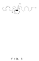
- FIG. 6 is a schematic showing an example where such an induction element 13 is inserted in parallel to the RFID tag IC 10 arranged at the feeding point in the dipole antenna, exemplified in Fig. 1.
- the induction element 13 is formed with a conductor line in a shape where a plurality of lines of the same shape, which are bent only at an obtuse angle, are provided in sequence similar to the antenna element 11. Accordingly, also for this induction element 13, its energy loss becomes small.
Abstract
An antenna line 11 is configured with a conductor line that meanders in a shape where a plurality of lines of the same shape, which are bent only at an obtuse angle, are provided in sequence.
Description
- The present invention relates to an antenna technique, and more particularly, to a technique for downsizing an antenna.
- An RFID (Radio Frequency Identification) technique is a technique for identifying a data carrier by using a radio wave without contact. With this technique, a tag (RFID tag) in which an IC chip and an antenna are embedded is attached to an object or a person, a device called an RFID reader/writer, and the RFID tag make a communication by using a radio wave, and the RFID reader/writer reads information stored in the IC chip (RFID tag IC), whereby the object or the person is identified.
- Fig. 7 shows a first example of an antenna available to an RFID tag. This antenna is a fundamental dipole antenna which is formed with
antenna lines 101, and the entire length of which is a 1/2 wavelength, and the RFID tag is configured by connecting this antenna to anRFID tag IC 10. - Additionally, Fig. 8 shows a second example of an antenna available to an RFID tag. This antenna is a fundamental loop antenna which is formed with an
antenna line 102, and the entire circumference of which is 1 wavelength, and the RFID tag is configured by connecting this antenna to anRFID tag IC 10. - As described above, the RFID tag becomes very large if the fundamental antenna such as a dipole antenna, a loop antenna, etc. is used unchanged. Therefore, the downsizing of the antenna is demanded for the RFID tag.
- A number of techniques for downsizing an antenna are proposed conventionally.
- For example. Fig. 9 shows a third example of an antenna available to an RFID tag. This antenna is downsized by bending a pair of
antenna lines 101, which forms the dipole antenna according to the first example shown in Fig. 7, in a shape meandering at a right angle. - Furthermore, Fig. 10 shows a fourth example of an antenna available to an RFID tag. This antenna is downsized by bending the loop-
shaped antenna line 102, which configures the loop antenna shown in Fig. 8, along a Hilbert fractal pattern. - Still further, Fig. 11 shows a fifth example of an antenna available to an RFID tag. This antenna is downsized by bending the loop-
shaped antenna line 102, which configures the loop antenna shown in Fig. 8, along a Koch fractal pattern. The fractal means that a portion of a graphic is self-similar to the entire graphic, for example, as shown in Fig. 12A depicting the partial view of a pattern of Fig. 11, and Fig. 12B depicting the outline of the pattern. Namely, a straight line portion of a large shape is replaced with a shape similar to the entire shape as in a relationship of replacing apattern 102a with apattern 102b, and a relationship of replacing thepattern 102b with apattern 102c in Fig. 12B. Therefore, a longer path length can be obtained by implementing the shape of theantenna line 102 to be a fractal pattern. - As described above, the technique using a conductor line, which is made to meander, as an antenna element is conventionally carried out.
- For example, Patent Document 1 discloses a technique for forming a loop antenna by arranging 2 coils upright on a ground conductor, and by connecting the 2 coils with a meandering line or plate conductor.
- Additionally, for example, Patent Document 2 discloses a technique for arranging and bending a pair of zigzag antenna elements, which configures a dipole antenna, along the inner wall surface of a housing.
- Furthermore, for example, Patent Document 3 discloses, for example, as shown in Fig. 13, a loop antenna the line conductor of which is bent in the shape of a snowflake.
- An antenna comprised by an RFID tag is not only demanded to be small as described above, but also desired to reduce an antenna gain in order to obtain a long communication distance. Additionally, for an RFID tag, so-called a passive tag, which does not comprise a battery within the RFID tag itself, and uses a radio wave from an RFID reader/writer as a power source for its operations, an antenna having high impedance is demanded to obtain a high power source voltage.
- However, if the antenna is downsized by making a conductor line, which is an antenna element, simply meander, degradations in a gain and impedance are caused in contradiction to the above described demands.
- Patent Document 1:
Japanese Unexamined Published Patent Application No. 2001-284935 - Patent Document 2:
Japanese Unexamined Published Patent Application No. 2000-349526 - Patent Document 3:
U.S. Patent Specification No. 6603440 (line 56 of column 9 - line 59 ofcolumn 10, Figs. 10A, 10B, 11A, 11B, 11C) - The present invention was developed in the light of the above described problems, and an object thereof is to prevent a gain from being degraded even if an antenna is downsized by making a conductor line, which is an antenna element, meander.
- An antenna according to one preferred embodiment of the present invention is characterized in that an antenna element is configured with a conductor line which meanders in a shape where a plurality of lines of the same shape, which are bent only at an obtuse angle, are provided in sequence, and solves the above described problems with this characteristic.
- With the above described configuration, the number of portions, which are bent at a right angle or an acute angle, of a conductor line configuring an antenna element decreases, whereby a loss in the energy of a high-frequency signal is reduced, and the emission efficiency of the antenna is improved as a result.
- In the above described antenna according to the present invention, the antenna element may configure a dipole antenna.
- Additionally, in the above described antenna according to the present invention, the antenna element may configure a loop antenna, the maximum point of an electric current in the antenna element when a high-frequency signal is fed may be arranged closer to the feeding point of the antenna element than the voltage maximum point of the antenna element at the time of the feeding.
- With this configuration, a line in the vicinity of the feeding point and that in the vicinity of the maximum point of the electric current are linked stronger, so that the impedance of the antenna can be made high.
- At this time, the length of the entire circumference of the antenna element, which configures the loop antenna, may be nearly one wavelength.
- Additionally, at this time, a line width at the maximum point of the electric current of the conductor line, which configures the antenna element, may be broader than that at the feeding point of the conductor line.
- With this configuration, an electric current made to flow into a feeding device provided at the feeding point is more difficult to flow than in the conductor line in the vicinity of the maximum point of the electric current, so that impedance becomes high.
- Furthermore, in the above described antenna according to the present invention, an induction element which cancels the capacitive component of the feeding device feeding a high-frequency signal to the antenna element may be comprised at the feeding point of the antenna element, and the induction element may be formed with a conductor line in a shape where a plurality of lines of the same shape, which, are bent only at an obtuse angle, are provided in sequence.
- With this configuration, an energy loss in the induction element is reduced.
- Also an RFID tag, which is characterized in that the above described antenna according to the present invention is comprised, relates to the present invention.
- The present invention is configured as described above, thereby producing an effect that degradation in a gain is reduced even if an antenna is downsized by making a conductor line, which is an antenna element, meander.
-
- Fig. 1 is a schematic showing a configuration example of an antenna implementing the present invention;
- Fig. 2A is a schematic showing a first example of a bending shape of a basic line which configures an antenna;
- Fig. 2B is a schematic showing a second example of a bending shape of a basic line which configures an antenna;
- Fig. 2C is a schematic showing a third example of a bending shape of a basic line which configures an antenna;
- Fig. 2D is a schematic showing a fourth example of a bending shape of a basic line which configures an antenna;
- Fig. 3 is a schematic showing an example of a loop antenna configured by making a current maximum point close;
- Fig. 4 is a schematic showing the results of a simulation of the current distribution of the loop antenna shown in Fig. 3;
- Fig. 5 is a schematic showing an example of a loop antenna where a line width in the vicinity of a current maximum point on a side opposite to a feeding point is made broad;
- Fig. 6 is a schematic showing an example where an induction element is inserted in parallel to an RFID tag IC arranged at a feeding point in the dipole antenna shown in Fig. 1;
- Fig. 7 is a schematic showing a first example of an antenna available to an RFID tag;
- Fig. 8 is a schematic showing a second example of an antenna available to an RFID tag;
- Fig. 9 is a schematic showing a third example of an antenna available to an RFID tag;
- Fig. 10 is a schematic showing a fourth example of an antenna available to an RFID tag;
- Fig. 11 is a schematic showing a fifth example of an antenna available to an RFID tag;
- Fig. 12A is a schematic showing a portion of the antenna shown in Fig. 11;
- Fig. 12B is a schematic explaining a fractal pattern of Fig. 11; and
- Fig. 13 is a schematic showing an example of a conventional loop antenna formed by bending a line conductor in the shape of a snowflake.
- Preferred embodiments according to the present invention are described below with reference to the drawings.
- Fig. 1 shows a configuration example of an antenna implementing the present invention. This antenna is a dipole antenna that is formed with a pair of
antenna lines 11, which are conductor lines, and has the entire length of a 1/2 wavelength, and an RFID tag is configured by connecting this antenna to anRFID tag IC 10. The shapes of the antenna elements (the pair of antenna lines 11), which form this antenna, are replaced with lines formed by bending a straight line portion of theantenna line 101, which is shown in Fig. 9 and bent at a right angle in a meandering shape, at an obtuse angle, so that the number of portions bent at a right angle (90°) or an acute angle decreases. - Normally, if a conductor line which configures an antenna element is bent at a right angle or an acute angle, the energy of a high-frequency signal to be emitted from an antenna is lost in that portion due to interference, etc., and emission efficiency as the whole of the antenna is degraded. Here, if the
antenna line 11 is replaced with the conductor line which is shown in Fig. 1 and bent at an obtuse angle, the number of portions, which are bent at a right angle or an acute angle, of the conductor line configuring the antenna element decreases, whereby the loss of the energy of a high-frequency signal is reduced, and the emission efficiency of the antenna is improved as a result. - In the example of Fig. 1, the dipole antenna is configured with the conductor line which meanders in a shape where a plurality of lines of the same shape, which are bent only at the obtuse angle, are provided in sequence. Alternatively, a loop antenna may be configured by replacing the straight line portions of the
antenna line 102, which is bent along a fractal pattern as shown in Figs. 10 and 11, with lines bent at an obtuse angle. The pattern of the replacedantenna line 102 is no longer fractal. - Additionally, in the above described example, the line of the same shape shown in Fig. 2A, namely, the line bent only at an obtuse angle such as 120° is adopted, and the antenna element is formed with the conductor line which meanders in a shape where a plurality of lines of the same shape as the adopted line are provided in sequence. However, a curve in the shape of a semicircle exemplified in Fig. 2B, or a curve in the shape of a sinusoidal wave of 1 period exemplified in Fig. 2C may be adopted instead of adopting the line of the above described shape. Besides, a line of combined shapes, which is exemplified in Fig. 2D, such as a shape obtained by combining the semicircle of Fig. 2B and the sinusoidal, wave of Fig. 2C may be adopted.
- Incidentally, as described above, for an RFID tag, which is a passive tag, an antenna having high impedance is demanded to gain a high power source voltage. In this point, the 1-waveiength loop antenna shown in Fig. 8 is desirable as an RFID tag because its impedance is high (normally on the order of 300 Ω). However, for the conventional loop antenna formed by bending the line conductor as exemplified in Fig. 13, a
feeding point 12a at which an RFID tag is connected, and apoint 12b which is the position of a 1/2 wavelength from thefeeding point 12a are far apart in theantenna line 12. In the 1-wavelength loop antenna, a high-frequency current becomes the maximum both at thefeeding point 12a and thepoint 12b in theantenna line 12. If these 2 points are far apart, the impedance is degraded to on the order of several tens of Ω. - Accordingly, as shown in Fig. 3, in the
antenna line 12, which is a conductor line meandering in the shape where the plurality of lines of the same shape, which are bent only at the obtuse angle, are provided in sequence, the loop antenna the entire circumference length of which is nearly 1 wavelength is configured by making thefeeding point 12a and thepoint 12b close and arranging them, and this antenna is used for the RFID tag. In consequence, the linkage between the line in the vicinity of thefeeding point 12a and that in the vicinity of thepoint 12b becomes strong, thereby improving the impedance. - Results of a computer simulation of the distribution of a high-frequency current when a high-frequency signal is fed to the loop antenna exemplified in Fig. 3 are shown in Fig. 4. This figure indicates that a larger current flows as the color gets dark. As is Known from this figure, it is proved that the
point 12b at which the high-frequency current becomes the maximum in theantenna line 12 is arranged closer to thefeeding point 12a than apoint 12c at which the high-frequency current becomes the minimum (namely, the point at which the high-frequency current becomes the maximum). - In the loop antenna exemplified in Fig. 3, if a line width in the vicinity of the
point 12b in theantenna line 12 is made broader than that in the vicinity of thefeeding point 12a as shown in Fig. 5, a current made to flow into the RFID tag IC provided at thefeeding point 12a is more difficult to flow than in theantenna line 12 in the vicinity of thepoint 12b, so that the impedance becomes high. - Incidentally, there are cases where an induction element for canceling the internal capacity of an RFID tag IC is connected in parallel to an antenna. Fig. 6 is a schematic showing an example where such an
induction element 13 is inserted in parallel to theRFID tag IC 10 arranged at the feeding point in the dipole antenna, exemplified in Fig. 1. In this example, theinduction element 13 is formed with a conductor line in a shape where a plurality of lines of the same shape, which are bent only at an obtuse angle, are provided in sequence similar to theantenna element 11. Accordingly, also for thisinduction element 13, its energy loss becomes small. - In addition, the present invention is not limited to the above described preferred embodiments, and various improvements and modifications can be made within a scope which does not deviate from the gist of the present invention.
- For example, the loop antenna shown in Figs. 3 and 5 is configured to be a line-symmetric shape, but the loop antenna may be configured to be an asymmetric shape.
Claims (7)
- An antenna where an antenna element is configured with a conductor line that meanders in a shape where a plurality of lines of a same shape, which are bent only at an obtuse angle, are provided in sequence.
- The antenna according to claim 1, wherein
the antenna element configures a dipole antenna. - The antenna according to claim 1, wherein
the antenna element configures a loop antenna, and a current maximum point of the antenna element when a high-frequency signal is fed is arranged closer to a feeding point of the antenna element than a voltage maximum point of the antenna element at the time of the feeding. - The antenna according to claim 3, wherein
a length of an entire circumference of the antenna element which forms the loop antenna is nearly 1 wavelength. - The antenna according to claim 3, wherein
a ling width at the current maximum point of the conductor line which configures the antenna element is broader than a line width at the feeding point of the conductor line. - The antenna according to claim 1, wherein:an induction element for canceling a capacitive component of a feeding device feeding a high-frequency signal to the antenna element is comprised at a feeding point of the antenna element; andthe induction element is formed with a conductor line in a shape where a plurality of lines of a same shape, which are bent only at an obtuse angle, are provided in sequence.
- An RFID tag comprising the antenna according to any one of claims 1 to 6.
Applications Claiming Priority (1)
| Application Number | Priority Date | Filing Date | Title |
|---|---|---|---|
| PCT/JP2005/004549 WO2006098004A1 (en) | 2005-03-15 | 2005-03-15 | Antenna and rfid tag |
Publications (2)
| Publication Number | Publication Date |
|---|---|
| EP1860728A1 true EP1860728A1 (en) | 2007-11-28 |
| EP1860728A4 EP1860728A4 (en) | 2008-12-24 |
Family
ID=36991364
Family Applications (1)
| Application Number | Title | Priority Date | Filing Date |
|---|---|---|---|
| EP05720805A Withdrawn EP1860728A4 (en) | 2005-03-15 | 2005-03-15 | Antenna and rfid tag |
Country Status (5)
| Country | Link |
|---|---|
| US (1) | US7773045B2 (en) |
| EP (1) | EP1860728A4 (en) |
| JP (1) | JPWO2006098004A1 (en) |
| CN (1) | CN101128956B (en) |
| WO (1) | WO2006098004A1 (en) |
Families Citing this family (6)
| Publication number | Priority date | Publication date | Assignee | Title |
|---|---|---|---|---|
| WO2007013167A1 (en) * | 2005-07-29 | 2007-02-01 | Fujitsu Limited | Rf tag and rf tag manufacturing method |
| JP5018884B2 (en) * | 2007-07-18 | 2012-09-05 | 富士通株式会社 | Wireless tag and wireless tag manufacturing method |
| WO2012070678A1 (en) * | 2010-11-26 | 2012-05-31 | 京セラ株式会社 | Antenna, dipole antenna, and communication device utilizing same |
| CN102509872A (en) * | 2011-10-24 | 2012-06-20 | 无锡邦普氿顺微电子有限公司 | UHF (ultra high frequency) RFID (radio frequency identification device) electronic label antenna |
| JP6161487B2 (en) * | 2013-09-24 | 2017-07-12 | 峰光電子株式会社 | Reading sensor and management system |
| US11213773B2 (en) | 2017-03-06 | 2022-01-04 | Cummins Filtration Ip, Inc. | Genuine filter recognition with filter monitoring system |
Citations (6)
| Publication number | Priority date | Publication date | Assignee | Title |
|---|---|---|---|---|
| US3716861A (en) * | 1971-03-22 | 1973-02-13 | J Root | Serpentine antenna mounted on a rotatable capacitive coupler |
| EP1058340A1 (en) * | 1998-12-25 | 2000-12-06 | Matsushita Electric Industrial Co., Ltd. | Antenna, radio device and radio repeater |
| WO2000077884A1 (en) * | 1999-06-10 | 2000-12-21 | Harada Industries (Europe) Limited | Multiband antenna |
| US20030132893A1 (en) * | 2001-10-29 | 2003-07-17 | Forster Ian J. | Wave antenna wireless communication device and method |
| US20030210188A1 (en) * | 2002-05-09 | 2003-11-13 | Ted Hebron | Multi-band antenna system including a retractable antenna and a meander antenna |
| US20050024287A1 (en) * | 2003-05-29 | 2005-02-03 | Young-Min Jo | Radio frequency identification tag |
Family Cites Families (20)
| Publication number | Priority date | Publication date | Assignee | Title |
|---|---|---|---|---|
| JPS6095711U (en) | 1983-12-06 | 1985-06-29 | 日本電気株式会社 | Cavity back slot antenna |
| US6104349A (en) * | 1995-08-09 | 2000-08-15 | Cohen; Nathan | Tuning fractal antennas and fractal resonators |
| US6452553B1 (en) * | 1995-08-09 | 2002-09-17 | Fractal Antenna Systems, Inc. | Fractal antennas and fractal resonators |
| JP2000349526A (en) | 1999-06-08 | 2000-12-15 | Hideo Suyama | Built-in antenna system |
| CN101188325B (en) * | 1999-09-20 | 2013-06-05 | 弗拉克托斯股份有限公司 | Multi-level antenna |
| JP4160215B2 (en) * | 1999-09-29 | 2008-10-01 | カルソニックカンセイ株式会社 | Air conditioner for vehicles |
| GB2355116B (en) | 1999-10-08 | 2003-10-08 | Nokia Mobile Phones Ltd | An antenna assembly and method of construction |
| CN1434988A (en) * | 2000-01-19 | 2003-08-06 | 弗拉克托斯股份有限公司 | Fractal and space-filling transmission lines, resonators filters and passive network elements |
| WO2001054225A1 (en) * | 2000-01-19 | 2001-07-26 | Fractus, S.A. | Space-filling miniature antennas |
| JP4221878B2 (en) | 2000-01-25 | 2009-02-12 | ソニー株式会社 | Antenna device |
| US6603440B2 (en) * | 2000-12-14 | 2003-08-05 | Protura Wireless, Inc. | Arrayed-segment loop antenna |
| US6642898B2 (en) * | 2001-05-15 | 2003-11-04 | Raytheon Company | Fractal cross slot antenna |
| ATE364911T1 (en) * | 2001-10-16 | 2007-07-15 | Fractus Sa | LOADED ANTENNA |
| AU2002351091A1 (en) * | 2001-10-29 | 2003-05-12 | Marconi Intellectual Property (Us) Inc | Wave antenna wireless communication device |
| JP2003271912A (en) * | 2002-03-14 | 2003-09-26 | Mitsubishi Materials Corp | Id tag, substrate for integrated circuit having id tag, method for manufacturing substrate for integrated circuit, and id detector |
| AU2003304171A1 (en) * | 2002-07-23 | 2005-01-21 | The Penn State Research Foundation | Fractile antenna arrays and methods for producing a fractile antenna array |
| JP3898598B2 (en) * | 2002-08-26 | 2007-03-28 | 株式会社ヨコオ | Transceiver module |
| JP2004112044A (en) | 2002-09-13 | 2004-04-08 | Furukawa Electric Co Ltd:The | Loop antenna |
| WO2005043680A1 (en) * | 2003-10-22 | 2005-05-12 | Fractal Antenna Systems, Inc. | Antenna system for radio frequency identification |
| US6975277B2 (en) * | 2003-11-21 | 2005-12-13 | Kyocera Wireless Corp. | Wireless communications device pseudo-fractal antenna |
-
2005
- 2005-03-15 EP EP05720805A patent/EP1860728A4/en not_active Withdrawn
- 2005-03-15 JP JP2007507974A patent/JPWO2006098004A1/en active Pending
- 2005-03-15 WO PCT/JP2005/004549 patent/WO2006098004A1/en not_active Application Discontinuation
- 2005-03-15 CN CN2005800487191A patent/CN101128956B/en not_active Expired - Fee Related
-
2007
- 2007-09-12 US US11/898,425 patent/US7773045B2/en not_active Expired - Fee Related
Patent Citations (6)
| Publication number | Priority date | Publication date | Assignee | Title |
|---|---|---|---|---|
| US3716861A (en) * | 1971-03-22 | 1973-02-13 | J Root | Serpentine antenna mounted on a rotatable capacitive coupler |
| EP1058340A1 (en) * | 1998-12-25 | 2000-12-06 | Matsushita Electric Industrial Co., Ltd. | Antenna, radio device and radio repeater |
| WO2000077884A1 (en) * | 1999-06-10 | 2000-12-21 | Harada Industries (Europe) Limited | Multiband antenna |
| US20030132893A1 (en) * | 2001-10-29 | 2003-07-17 | Forster Ian J. | Wave antenna wireless communication device and method |
| US20030210188A1 (en) * | 2002-05-09 | 2003-11-13 | Ted Hebron | Multi-band antenna system including a retractable antenna and a meander antenna |
| US20050024287A1 (en) * | 2003-05-29 | 2005-02-03 | Young-Min Jo | Radio frequency identification tag |
Non-Patent Citations (2)
| Title |
|---|
| KRISCHKE A ED - ROTHAMMEL K: "Rothammels's Antennenbuch, passage" ROTHAMMELS ANTENNENBUCH, DARC VERLAG, BAUNATAL, 1 January 2001 (2001-01-01), pages 129-130, XP002455790 ISBN: 978-3-88692-033-4 * |
| See also references of WO2006098004A1 * |
Also Published As
| Publication number | Publication date |
|---|---|
| CN101128956A (en) | 2008-02-20 |
| EP1860728A4 (en) | 2008-12-24 |
| US20080012773A1 (en) | 2008-01-17 |
| CN101128956B (en) | 2012-11-21 |
| JPWO2006098004A1 (en) | 2008-08-21 |
| US7773045B2 (en) | 2010-08-10 |
| WO2006098004A1 (en) | 2006-09-21 |
Similar Documents
| Publication | Publication Date | Title |
|---|---|---|
| EP2330684B1 (en) | Rfid tag, rfid tag set and rfid system | |
| JP5018884B2 (en) | Wireless tag and wireless tag manufacturing method | |
| JP4711692B2 (en) | Meander line antenna | |
| JP4226642B2 (en) | RF tag and method of manufacturing RF tag | |
| JP5086004B2 (en) | Tag antenna and tag | |
| KR100998779B1 (en) | Rf tag and rf tag manufacturing method | |
| JP4755921B2 (en) | RFID tag | |
| JP4498364B2 (en) | Antenna and contactless tag | |
| KR100833431B1 (en) | Cross dipole antenna and tag using the same | |
| JP2007096655A (en) | Antenna for rfid tag and rfid tag | |
| CA2938640C (en) | Electronic payment terminal and coupling device | |
| KR20080012883A (en) | Rfid antenna | |
| US7773045B2 (en) | Antenna and RFID tag | |
| JPWO2006134658A1 (en) | RFID tag antenna and RFID tag | |
| AU2006346817A1 (en) | Antenna for near field and far field radio frequency identification | |
| JP4676445B2 (en) | Antenna and RFID tag equipped with the same | |
| KR20180131620A (en) | IC tag and manufacturing method of IC tag | |
| JP2007081632A (en) | Radio ic tag | |
| JP4922984B2 (en) | RFID antenna and RFID tag | |
| JP5218251B2 (en) | RFID tag reader | |
| JP5187083B2 (en) | RFID tag, RFID system, and RFID tag manufacturing method | |
| KR20080050022A (en) | Bow tie type antenna, radio frequency identification tag including the same and impedance matching method thereof | |
| JP6746058B2 (en) | Wireless IC tag device and wireless IC tag built-in device | |
| KR100924427B1 (en) | Antenna and rfid tag | |
| KR100690849B1 (en) | Printing antenna of uhf band |
Legal Events
| Date | Code | Title | Description |
|---|---|---|---|
| PUAI | Public reference made under article 153(3) epc to a published international application that has entered the european phase |
Free format text: ORIGINAL CODE: 0009012 |
|
| 17P | Request for examination filed |
Effective date: 20071010 |
|
| AK | Designated contracting states |
Kind code of ref document: A1 Designated state(s): DE FR GB |
|
| DAX | Request for extension of the european patent (deleted) | ||
| RBV | Designated contracting states (corrected) |
Designated state(s): DE FR GB |
|
| A4 | Supplementary search report drawn up and despatched |
Effective date: 20081124 |
|
| 17Q | First examination report despatched |
Effective date: 20090925 |
|
| STAA | Information on the status of an ep patent application or granted ep patent |
Free format text: STATUS: THE APPLICATION IS DEEMED TO BE WITHDRAWN |
|
| 18D | Application deemed to be withdrawn |
Effective date: 20161001 |