EP1860531A2 - Display device equipped with a touch panel - Google Patents
Display device equipped with a touch panel Download PDFInfo
- Publication number
- EP1860531A2 EP1860531A2 EP07108675A EP07108675A EP1860531A2 EP 1860531 A2 EP1860531 A2 EP 1860531A2 EP 07108675 A EP07108675 A EP 07108675A EP 07108675 A EP07108675 A EP 07108675A EP 1860531 A2 EP1860531 A2 EP 1860531A2
- Authority
- EP
- European Patent Office
- Prior art keywords
- touch panel
- display
- section
- panel
- display device
- Prior art date
- Legal status (The legal status is an assumption and is not a legal conclusion. Google has not performed a legal analysis and makes no representation as to the accuracy of the status listed.)
- Withdrawn
Links
Images


Classifications
-
- G—PHYSICS
- G06—COMPUTING OR CALCULATING; COUNTING
- G06F—ELECTRIC DIGITAL DATA PROCESSING
- G06F3/00—Input arrangements for transferring data to be processed into a form capable of being handled by the computer; Output arrangements for transferring data from processing unit to output unit, e.g. interface arrangements
- G06F3/01—Input arrangements or combined input and output arrangements for interaction between user and computer
- G06F3/03—Arrangements for converting the position or the displacement of a member into a coded form
- G06F3/041—Digitisers, e.g. for touch screens or touch pads, characterised by the transducing means
- G06F3/0412—Digitisers structurally integrated in a display
-
- G—PHYSICS
- G02—OPTICS
- G02F—OPTICAL DEVICES OR ARRANGEMENTS FOR THE CONTROL OF LIGHT BY MODIFICATION OF THE OPTICAL PROPERTIES OF THE MEDIA OF THE ELEMENTS INVOLVED THEREIN; NON-LINEAR OPTICS; FREQUENCY-CHANGING OF LIGHT; OPTICAL LOGIC ELEMENTS; OPTICAL ANALOGUE/DIGITAL CONVERTERS
- G02F1/00—Devices or arrangements for the control of the intensity, colour, phase, polarisation or direction of light arriving from an independent light source, e.g. switching, gating or modulating; Non-linear optics
- G02F1/01—Devices or arrangements for the control of the intensity, colour, phase, polarisation or direction of light arriving from an independent light source, e.g. switching, gating or modulating; Non-linear optics for the control of the intensity, phase, polarisation or colour
- G02F1/13—Devices or arrangements for the control of the intensity, colour, phase, polarisation or direction of light arriving from an independent light source, e.g. switching, gating or modulating; Non-linear optics for the control of the intensity, phase, polarisation or colour based on liquid crystals, e.g. single liquid crystal display cells
- G02F1/133—Constructional arrangements; Operation of liquid crystal cells; Circuit arrangements
- G02F1/1333—Constructional arrangements; Manufacturing methods
-
- G—PHYSICS
- G06—COMPUTING OR CALCULATING; COUNTING
- G06F—ELECTRIC DIGITAL DATA PROCESSING
- G06F3/00—Input arrangements for transferring data to be processed into a form capable of being handled by the computer; Output arrangements for transferring data from processing unit to output unit, e.g. interface arrangements
- G06F3/01—Input arrangements or combined input and output arrangements for interaction between user and computer
- G06F3/03—Arrangements for converting the position or the displacement of a member into a coded form
- G06F3/041—Digitisers, e.g. for touch screens or touch pads, characterised by the transducing means
- G06F3/045—Digitisers, e.g. for touch screens or touch pads, characterised by the transducing means using resistive elements, e.g. a single continuous surface or two parallel surfaces put in contact
Definitions
- the present invention relates to a display device equipped with a touch panel, the display device allowing input operations using a display surface of a display panel by disposing a touch panel on the display surface of the display panel accessible through an opening section of a device housing.
- Patent Document 1 describes what is related to a liquid crystal display device equipped with a liquid crystal panel integrated with a touch panel.
- the liquid crystal device described in Patent Document 1 is characterized in that "in the liquid crystal display device having a liquid crystal display panel with a transparent touch panel stacked on the display surface side thereof housed in a case with a display window, the case is made to support only the touch panel, and the back face of the liquid crystal display panel is made a predetermined length distant from the inside surface of the case.”
- the touch panel provided to the liquid crystal display device described in Patent Document 1 is a so-called resistive-film touch panel having a pair of film substrates 2a, 2b each provided with a transparent electrode on the surface facing each other and a spacer 2c intervening between the pair of film substrates 2a, 2b.
- the resistive-film touch panel is arranged so that the transparent electrode of the film substrate 2a touches the transparent electrode of the film substrate 2b in response to the film substrate 2a being pressed, thus the position of the pressed area is detected to perform an input operation.
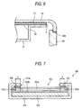
- Fig. 7 shows an example of the display device of the related art equipped with such a resistive-film touch panel.
- the display device 100 shown in Fig. 7 is composed of a device chassis 101 provided with an opening section 101a, a display panel 102 housed inside the device chassis 101 and having a display surface accessible through the opening section 101a, a touch panel 103 disposed in the display surface of the display panel, a seal member 104 intervening between the touch panel 103 and the device chassis 101, and so on.
- the touch panel 103 which is of the resistive-film, is composed of an upper substrate 103a and a lower substrate 103b each provided with a transparent conductive film (corresponding to the transparent electrode of the touch panel according to Patent Document 1) on the surface thereof facing each other, bar-like cushion members 103c disposed between the peripheries of the upper substrate 103a and the lower substrate 103b, and so on.
- a pressing operation performed on a peripheral area X of the cushion member 103c will cause strong force applied on the upper substrate 103a taking a corner of the cushion member 103c as the fulcrum.
- the transparent conductive film provided to the upper substrate 103a is brittle in nature, if the distance from the point on which the pressing operation is performed to the corner of the cushion member 103c is short, the transparent conductive film might be broken. Therefore, in the display device 100 of the related art, by covering the area X with the rim of the opening section 101a of the device chassis 101, the pressing operation on the area X has been prevented.
- the display device having such a configuration, since the area X, which might be broken by the pressing operation thereon is covered with the rim of the opening section 101a of the device chassis 101, a step has been caused between the surface of the device main body 101 and the surface of the touch panel 103. Therefore, the display device easily gets dirty with foreign particles such as dust accumulated in the step section between the device chassis 101 and the touch panel 103, resulting in problems of a cumbersome work for removing the dirt and of a low visual quality of the appearance thereof, from the view point of design.
- the step is caused between the surface of the device chassis and the surface of the touch panel resulting in the dirtiness with the foreign particles such as dust accumulated in the step section and the low visual quality of the whole device.
- a display device equipped with a touch panel including a device chassis provided with an opening section, a display panel having a display surface disposed accessible through the opening section, a touch panel disposed on the display surface of the display panel and capable at least of selecting a function displayed on the display surface in response to a pressing operation on the touch panel, and a surface sheet for covering the touch panel on the opposite side to the display panel, and closing the opening section to form substantially the same surface with the device chassis, wherein a reinforcing area for improving resistivity against pressing force applied from the outside is provided in a predetermined range of the surface sheet.
- the display device equipped with a touch panel of the embodiment of the invention by providing the surface sheet for covering the touch panel disposed on the display panel and for closing the opening section of the device chassis to form a part of the device chassis, one surface of the device chassis through which the display panel provided with the touch panel is accessible can be made planar. As a result, dirtiness with the foreign particles such as dust accumulated in one surface of the device chassis can be prevented, and the visual quality of the whole device can be improved. Moreover, by providing the reinforcing area with improved resistivity against the pressing force applied from the outside in the surface sheet, the concentrated stress can be prevented from locally acting on the touch panel covered with the reinforcing area, thus the breakage of the transparent conductive film of the touch panel can be prevented.
- a display device equipped with a touch panel which can improve the visual quality of the whole device by forming an opening section of a device chassis, which the touch panel is stacked on a display panel accessibly through, as a plane without a step, and can prevent breakage of a transparent conductive film of the touch panel, is realized with a simple configuration.
- Figs. 1 through 6 are for explaining the embodiments of the invention.
- Fig. 1 is a perspective view from the front side of a digital still camera showing a first embodiment of the display device equipped with a touch panel according to the invention
- Fig. 2 is a perspective view from the rear side of the digital still camera shown in Fig. 1
- Fig. 3 is an exploded explanatory view separating a touch panel, a surface sheet, and so on from the digital still camera shown in Fig. 1
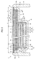
- Fig. 4 is a cross-sectional explanatory view of the digital still camera shown in Fig. 1 showing the states of the touch panel, the surface sheet, and so on
- Fig. 1 is a perspective view from the front side of a digital still camera showing a first embodiment of the display device equipped with a touch panel according to the invention
- Fig. 2 is a perspective view from the rear side of the digital still camera shown in Fig. 1
- Fig. 3 is an exploded explanatory view separating a touch panel,
- FIG. 5 is a cross-sectional explanatory view for explaining a second embodiment of the display device equipped with a touch panel according to the invention
- Fig. 6 is a cross-sectional explanatory view for explaining a third embodiment of the display device equipped with a touch panel according to the invention.
- Figs. 1 and 2 show a digital still camera 1 applied as the first embodiment of an imaging apparatus showing a specific example of a display device equipped with a touch panel according to the invention.
- the digital still camera 1 is arranged to use a semiconductor recording medium as an information recording medium, and to be able to convert an optical image from the subject into an electric signal using imaging means such as CCD (a solid-state imaging device) to record it on the semiconductor recording medium, or to display it on a display panel such as a liquid crystal display.
- imaging means such as CCD (a solid-state imaging device) to record it on the semiconductor recording medium, or to display it on a display panel such as a liquid crystal display.
- the digital still camera 1 is configured including a camera case 2 showing a specific example of a device chassis, a lens body tube 3 for acquiring an image of the subject as light and leading the light to an imaging device such as CCD or CMOS as imaging means, a liquid crystal panel 4 showing a specific example of a display panel for displaying an image in accordance with a video signal output from the imaging device, a touch panel 5 disposed on a display surface of the liquid crystal panel 4 and capable of selecting a function, which is displayed on the display surface of the liquid crystal panel 4, in response to a pressing operation thereon, a surface sheet 6 for covering a surface of the touch panel 5 opposite to the liquid crystal panel 4, a control device for controlling an operation of the lens body tube 3, display of the liquid crystal panel 4, and so on, a battery power supply not shown, and so on.
- a camera case 2 showing a specific example of a device chassis
- a lens body tube 3 for acquiring an image of the subject as light and leading the light to an imaging device such as CCD or CMOS
- the camera case 2 is composed of a front case 7 and a rear case 8 each formed of an elongated flat vessel and overlapped each other in an anteroposterior direction, a center case 9 formed of a substantially rectangular frame intervening between the front case 7 and the rear case 8, and so on.
- a control device for driving and controlling the lens body tube 3, the liquid crystal panel 4, and so on.
- the control device is composed of, for example, a wiring board on which a predetermined electric circuit is formed by a printing formation method or the like, electronic components such as a microcomputer, resistors, or capacitors mounted at predetermined positions on the wiring board, and so on.
- a decorative ring 10 is attached to the front case 7 on the front surface at a position a little bit shifted from the center thereof, and the lens body tube 3 is provided movably in a back and forth direction through a center hole of the decorative ring 10.
- the lens body tube 3 is a so-called retractable lens which has a configuration capable of expanding and contracting in a nested manner, and is retracted inside the camera case 2 when shooting is not performed. It is arranged that the front surface of the lens body tube 3 in a field lens 3A side forms substantially the same plane with the front surface of the front case 7 when the lens body tube 3 is retracted.
- the front case 7 is provided with a light emitting section 12 of a flash unit and a light emitting/receiving section 13 of an automatic focus mechanism at obliquely upward positions of the lens body tube 3. Further, on the upper surface of the center case 9, there are provided a power button 15, a shutter release button 16, sound collecting holes 17 of a sound collecting device such as a microphone, and so on. Further, on one side surface of the center case 9, there is provided a battery storage section for detachably storing a battery as a power source, and the battery storage section is provided with a battery lid 18 detachably attached thereto. Further, on the opposite side section of the center case 9 to the battery lid 18, there are provided speaker holes 19 for a speaker unit.
- a mode selection switch 21 for selecting a functional mode (e.g., a still image mode, a movie mode, or a play back mode).
- a functional mode e.g., a still image mode, a movie mode, or a play back mode.
- an opening section 23 is provided to the rear case 8 so as to open a substantially entire area of the rear face of the camera case 2.
- a liquid crystal panel assembly 31 having the liquid crystal panel 4, a backlight assembly 41 disposed behind the liquid crystal panel assembly 31, a support member 51 for supporting the backlight assembly 41 and the liquid crystal panel assembly 31, and the touch panel 5 disposed and stacked on a display surface 4a of the liquid crystal panel 4.
- the surface sheet 6 for covering the touch panel 5 and at the same time sealing the opening section 23.
- the liquid crystal panel assembly 31 is composed of the liquid crystal panel 4, a panel frame 32 for holding the liquid crystal panel 4, and so on.
- the liquid crystal panel 4 has an elongated rectangular plane shape, and is composed of an upper polarization plate 33, an upper glass plate 34, a liquid crystal layer 35, a lower glass plate 36, and a lower polarization plate 37 stacked in this order from the side of the opening section 23 of the rear case 8.
- the upper polarization plate 33 and the lower polarization plate 37 of the liquid crystal panel 4 are for aligning the vibration of light passing therethrough to one direction to control the light intensity.
- the upper and lower polarization plates 33, 37 are arranged to be smaller than the upper and lower glass plates 34, 36 and are disposed through openings 38a, 39a of the panel frame 32 described later, respectively. Further, the surface of the upper polarization plate 33 forms the display surface 4a of the liquid crystal panel 4.
- the panel frame 32 is formed of a combination of an outer frame 38 discretely formed as a separated member and an inner frame 39 formed to be a little bit smaller than the outer frame 38.
- the outer frame 38 and the inner frame 39 are formed of rectangular frames having rectangular opening sections 38a, 39a with sizes corresponding to the upper and lower polarization plates 33, 37, respectively, and the panel frame 32 is composed integrally by combining the inside edge of the outer frame 38 and the outside edge 39 of the inner frame 39.
- the both inside edges of the shorter sides of the outer frame 38 are each provided with an engaging protrusion not shown, and the both outside edges of the shorter sides of the inner frame 39 are each provided with an engaging recess to be engaged with the corresponding engaging protrusion of the outer frame 38.
- the engaging protrusions and the engaging recesses are arranged to be respectively engaged with each other when the inside edge of the outer frame 38 and the outside edge of the inner frame 39 are overlapped each other, thus the outer frame 38 and the inner frame 39 are reliably fixed to each other and configured integrally.
- a notch 38b opening downward.
- a notch 39b opening upward corresponding to the notch 38b of the outer frame 38.
- the notches 38b, 39b form a through hole on the side face of the panel frame 32 assembled integrally with the outer frame 38 and the inner frame 39. Further, the through hole of the panel frame 32 is provided with a flexible wiring board 25a connected therethrough to the liquid crystal panel 4.
- the configuration of providing the engaging protrusions on the inside edge of the outer frame 38, and providing the engaging recesses on the outside edge of the inner frame 39 is adopted, it is obvious that a reversed configuration of providing the engaging recesses on the inside edge of the outer frame 38, and providing the engaging protrusions on the outside edge of the inner frame 39 can also be adopted.
- the panel frame 32 can also be integrally configured by fixing the outer frame 38 and the inner frame 39 with fixing means such as a plurality of fixing screws or an adhesive.
- the backlight assembly 41 is composed of a backlight main body 42, a light frame 43 for holding the backlight main body 42, and so on.
- the backlight main body 42 is light source means for supplying the liquid crystal panel 4 with light, and has a plane shape with substantially the same size as the liquid crystal panel 4.
- a so-called light emitting diode (LED) backlight using a white LED as the light source a so-called electroluminescence (EL) backlight using an EL light emitter as the light source, and so on can be cited.
- LED light emitting diode
- EL electroluminescence
- the light frame 43 is composed of a combination of an outer frame 45 discretely formed as a separated member and an inner frame 46 formed to be a little bit smaller than the outer frame 45, and the size is arranged to be substantially the same as the panel frame 32.
- the outer frame 45 of the light frame 43 forms a rectangular frame having an opening section 45a for exposing the backlight main body 42, and the inner frame 46 forms a chassis with the upper side open. Further, by combining the inside edge of the outer frame 45 and the side face of the inner frame 46, the light frame 43 is integrally configured.
- engaging protrusions not shown, respectively.
- engaging recesses not shown, respectively, to be engaged with the engaging protrusions of the outer frame 45, similarly to the inner frame 39 of the panel frame 32.
- the engaging protrusions and the engaging recesses are arranged to be respectively engaged with each other when the inside edge of the outer frame 45 and the outside edge of the inner frame 46 are overlapped each other, thus the outer frame 45 and the inner frame 46 are reliably fixed to each other and configured integrally.
- a notch opening upward so as to correspond to the notch 45b of the outer frame 45. It is arranged that a through hole is provided to the side face of the light frame 43 with the notch of the inner frame 46 and the notch 45b of the outer frame 45.
- the through hole of the light frame 43 is provided with a flexible wiring board 25b connected therethrough to the backlight main body 42.
- the liquid crystal panel assembly 31 and the backlight assembly 41 are supported by the support member 51 in the condition in which the backlight assembly 41 is stacked on the rear side of the liquid crystal panel assembly 31.
- the support member 51 is composed of a substantially rectangular base plate 52 on which the liquid crystal panel assembly 31 and the backlight assembly 41 stacked one another are mounted, a plurality of holding segments 53 extending substantially perpendicular to the base plate 52 and continuously to the three sides thereof, a support section 54 provided continuously to the remaining side of the base plate 52 and for supporting an expanded section 5a of the touch panel 5 described later, and so on.
- the base plate 52 of the support member 51 is arranged to have a size compatible with the liquid crystal panel assembly 31 and the backlight assembly 41. Further, by attaching the base plate 52 on a fixing section not shown of the center case 9 with fixing means such as fixing screws, the support member 51 is fixed inside the camera case 2.
- five holding segments are provided as the plurality of holding segments 53 of the support member 51, and two of them are disposed in the middle of each of the two longer sides of the base plate 52 with an appropriate distance and one is disposed in the middle of a shorter side thereof.
- These five holding segments 53 are for holding the liquid crystal panel assembly 31 and the backlight assembly 41 by pinching the sides thereof, and are arranged to have lengths equal to the height of the stack of the both assemblies 31, 41.
- the support section 54 of the support member 51 is composed of a rising segment 56 extending substantially vertically and continuously from the opposing short side to the one short side provided with the holding segment 53, and an expansion segment 57 expanded in a parallel direction to the base plate 52 continuously to the rising segment 56 and for mounting the expanded section 5a of the touch panel 5.
- the rising segment 56 of the support section 54 is provided with a through hole for allowing a flexible wiring board 28b connected to the backlight main body 42 be inserted therethrough.
- the expanded segment 57 of the support section 54 has a substantially rectangular shape with a size compatible with the expanded section 5a of the touch panel 5, and the upper surface thereof is arranged to have the same height as that of the upper surface of the liquid crystal panel assembly 31 supported by the support member 51, namely the display surface 4a of the liquid crystal panel 4.
- the touch panel 5 has an elongated rectangular planar shape, and is configured including an upper film member 61, a lower film member 62 opposing to the upper film member 61, an upper transparent conductive film 63 and a lower transparent conductive film 64 respectively disposed on the surfaces of the film members 61, 62 opposing to each other, a cushion member 65 intervening between both of the film members 61, 62, a dot spacer 66 for preventing short circuit between the upper transparent conductive film 63 and the lower transparent conductive film 64 while no pressing (touch) operation is performed, a polarization plate 67 disposed on the opposite side of the upper film member 61 to the lower film member 62, and so on as shown in Fig. 4.
- the material of the upper film member 61 and the lower film member 62 polyethylene terephthalate (PET) can be cited, but is not limited thereto. It is obvious that various kinds of materials used for this kind of film member such as polycarbonate (PC), polyethersulfone (PES), or polyarylate (PAR) can also be used therefor.
- the upper transparent conductive film 63 and the lower transparent conductive film 64 are members capable of conducting light and electricity, and indium tin oxide (ITO), which is typically used for this kind of touch panel, is applied thereto in the present embodiment.
- ITO indium tin oxide
- the upper and lower surfaces of the cushion member 65 are adhered to the upper film member 61 and the lower film member 62 with adhesion means such as an adhesive and an adhesive tape, thus a microscopic gap is formed between the upper and the lower film members 61, 62.
- adhesion means such as an adhesive and an adhesive tape
- an insulating elastic body such as rubber is preferably used. It is obvious, however, that various materials applied to this kind of cushion member such as flexible plastic or other materials can also be used therefor.
- a pressing (touch) operation within a predetermined area inner than the cushion member 65 of the touch panel 5 causes strong force applied to the upper film member 61 pivoting around the inside corner section of the cushion member 65.
- the upper transparent conductive film 63 which is brittle in nature, disposed on the upper film member 61 might be broken.
- the touch panel 5 includes a conductive film breakage occurring area A where the upper transparent conductive film 63 might be broken by a pressing operation, as shown in Fig. 4. This conductive film breakage occurring area A is covered by a reinforcing area C of the surface sheet 6 described later.
- the touch panel 5 is arranged to have longer sides longer than the liquid crystal panel assembly 31, thus one of the shorter sides thereof protrudes from the outside edge of the liquid crystal panel assembly 31 to form the expanded section 5a.
- the expanded section 5a of the touch panel 5 is provided with a plurality of input sections.
- the plurality of input sections is a switch mechanism utilizing the touch panel function, and it is arranged that various inputs to the digital still camera 1 are performed in response to a pressing operation on the switch mechanism.
- a zoom input section 68a for performing a zoom operation
- a menu input section 68b for selecting various menus
- a display switching input section 68c for switching the screen display.
- These input sections 68a through 68c face an input section operation area D of the surface sheet 6 described later.
- a direction operation input section for moving a cursor or the like for selecting items from a menu
- a screen operation input section for performing switching of the screen sizes or deletion of the screen, and so on.
- the touch panel 5 is fixed by bonding to the display surface 4a of the liquid crystal panel 4 and the expanded segment 57 of the support member 51 with an adhesive 69.
- the adhesive 69 is liquid-tightly filled at least between the touch panel 5 and the display surface 4a of the liquid crystal panel 4, thus preventing an air layer from intervening between the touch panel 5 and the display surface 4a of the liquid crystal panel 4 to avoid increase in the optical interfacial reflection.
- the surface sheet 6 has an elongated rectangular plane shape arranged to have a size compatible with the opening section 23 of the rear case 8, and arranged to seal the opening section 23, and at the same time, to form substantially the same plane with the rear case 8.
- the surface sheet 6 is formed of a transparent synthetic resin, which can be distorted to the extent that a pressing operation can be performed on the touch panel 5.
- an acrylic resin with a thickness arranged in a range of about 0.2mm through 0.5mm is preferable.
- Other synthetic resins such as polycarbonate can also be used with a thickness arranged so that the resin can be distorted to the extent that a pressing operation can be performed on the touch panel 5.
- the surface sheet 6 is provided with a display surface operating area B facing the display surface 4a of the liquid crystal panel 4 via the touch panel 5, a reinforcing area C provided to substantially the entire area in a range from the outside edge of the surface sheet 6 to the display surface operating area B and for covering the conductive film breakage occurring area A of the touch panel 5, and an input section operating area D facing each of the input sections 68a through 68c of the touch panel 5.
- the display surface operating area B of the surface sheet 6 is an area of the transparent synthetic resin used as the surface sheet without any modifications, through which the display surface 4a of the liquid crystal panel 4 can be viewed, and can be distorted to the extent that the pressing operation can be performed on the touch panel 5.
- the display surface operating area B can be made a little bit, for example, about 0.3mm outer from the periphery of the display surface 4a, larger than the display surface 4a of the liquid crystal panel 4.
- the meaning of 0.3mm mentioned here is as follows.
- the offset value the dimensional tolerance of the display surface operating area B in the surface sheet 6, the dimensional tolerance of the display surface 4a in the liquid crystal panel 4, the bonding tolerance between the surface sheet 6 and the liquid crystal panel 4, and so on can be absorbed, thus preventing the reinforcing area C from covering the display surface 4a.
- a so-called black mask formed as an area only for displaying black color.
- the reinforcing area C is formed by executing a serigraph 71 showing a specific example of coating on an opposite surface of the surface sheet 6 to the touch panel 5. Therefore, the reinforcing area C becomes an opaque layer, which blocks the light visible to the human, and it is arranged that the inside of the camera case 2 cannot be seen through the reinforcing area C. Thus, the reinforcing area C covers the conductive film breakage occurring area A, and at the same time, clarifies the boundary with the display surface operating area B.
- a coating material for enhancing rigidity is used as the coating material for the serigraph 71. This is for enhancing rigidity of the reinforcing area C to be higher than that of other areas, thus improving the resistivity of the reinforcing area C against the pressing force applied from the outside.
- the reinforcing area C is arranged not to be distorted to the extent that the pressing operation is performed on the touch panel 5 beneath the reinforcing area C.
- the coating material for enhancing rigidity a resin coating materials with high rigidity (e.g., resin paints containing metal) can be cited, but these are not limitations, and aluminum, silver, or the like can also be used. Further, it is also possible to arrange the color of the coating material to be the same as the camera case 2 to show as if the reinforcing area C is a part of the camera case 2.
- the reinforcing area C is formed by coating the coating material for enhancing the rigidity on the surface sheet 6, the formation of the reinforcing area C is not limited thereto.
- the reinforcing area C can be formed by adhering a material with high rigidity such as a metal foil, hardened plastic, or the like to the surface sheet 6, or performing a plating process thereon.
- the input section operating area D is composed of a zoom input operating area D1 facing a zoom input section 68a provided to the expanded section 5a of the touch panel 5, a menu input section operating area D2 facing the menu input section 68b, and a display switching input section operating area D3 facing the display switching input section 68c.
- Each of the input section operating areas D1 through D3 is, as is the case with the display surface operating area B, formed of the transparent synthetic resin without any modifications, and can be distorted to the extent that pressing operations can be executed on each of the input sections 68a through 68c of the touch panel 5.
- the input section operating areas D1 through D3 of the surface sheet 6 and the respective input sections 68a through 68c provided to the expanded section 5a of the touch panel 5 form various kinds of operation switches such as the menu operation switch or the display selection switch. These operation switches are provided instead of typically used mechanical tact switches, thereby reducing the number of components in comparison with the case of using the tact switches. Further, the face of the camera case 2 on which the liquid crystal panel 4 is disposed can be made as a single plane throughout the entire surface, thus the appearance of the whole digital still camera 1 can be improved.
- the various kinds of operation switches are formed by the respective input section operating areas D1 through D3 and respective input sections 68a through 68c
- the surface of the input section operating areas D1 through D3 facing the touch panel is provided with marks by printing or coating with different color from the color of the reinforcing area C for identification.
- the printing or the coating in this case hot stamp or serigraph, as is the case with the reinforcing area C can be cited.
- the coating material of the coating provided to the input section operating areas D1 through D3 a material with low rigidity is used to arrange that the input section operating areas D1 through D3 can be distorted to the extent that pressing operations can be performed on each of input sections 68a through 68c.
- the surface sheet 6 is fixed to a sheet fixing section 23a provided on the periphery of the opening section 23 of the rear case 8 and the opposite surface of the touch panel 5 to the liquid crystal panel 4 with an adhesive 72.
- This adhesive 72 is filled in at least between the surface sheet 6 and the touch panel 5 in a liquid-tight manner to prevent the air layer from intervening between the surface sheet 6 and the touch panel 5, thereby preventing increase in the optical interfacial reflection.
- shooting can be performed as follows, for example. Firstly, the digital still camera 1 is powered on by pushing the power button 15. Then, the still image mode is selected by the mode selection switch 21. Then, the menu operation switch composed of the menu input section 68b and the menu input section operating area D2 is pushed. Thus, the selection menu for performing settings of shutter speed, aperture, exposure, and so on is displayed on the display surface 4a of the liquid crystal panel 4.
- the settings of shutter speed, aperture, exposure, and so on are performed by pressing the selection menu displayed on the display surface 4a of the liquid crystal panel 4.
- the pressing operation is performed on the touch panel 5 overlapped on the display surface 4a of the liquid crystal panel 4 by pressing the display surface operating area B of the surface sheet 6 facing the display surface 4a of the liquid crystal panel 4, thus inputting settings of the shutter speed and so on.
- the display surface operating area B of the surface sheet 6 is arranged to be distorted to the extent that the pressing operation can be performed on the touch panel 5, the pressing operation can reliably be performed on the touch panel 5, thus the settings of the shutter speed and so on can be input.
- the reinforcing area C of the display panel 6, which is increased in resistivity against the pressing force applied from the outside by providing the serigraph 71, is not distorted to the extent that the pressing operation is performed on the touch panel 5 beneath the reinforcing area C.
- the concentrated stress can be prevented from acting on the conductive film breakage occurring area A covered by the reinforcing area C, thereby eliminating the concern that the upper transparent conductive film 63 of the touch panel 5 might be broken.
- an image of the subject acquired by the lens body frame 3 is displayed on the display surface 4a of the liquid crystal panel 4. After then, by pushing the shutter button, a still image can be shot.
- Fig. 5 is a cross-sectional explanatory view for explaining a second embodiment of the display device equipped with a touch panel according to the invention.
- the second embodiment has the support member formed integrally with the rear case, and has the only difference from the first embodiment in the support member 81. Therefore, only the support member 81 will be explained here, and the portions common to the first embodiment are denoted with the same reference numerals, and duplicated explanations will be omitted.
- the support member 81 is provided with a base plate 82, a plurality of holding segments 83, and a support section 84. Further, an opposite end portion of each of the plurality of holding segments 83 to the base plate 82 and an opposite end portion of the support section 84 to the base plate 82 are formed continuously to a sheet fixing section 85a of the rear case 85. In this case, the operation of fixing the support member 81 to the center case 9 can be eliminated, thus making it possible to reduce man-hour.
- Fig. 6 is a cross-sectional explanatory view for explaining a third embodiment of the display device equipped with a touch panel according to the invention.
- the digital still camera 90 of the second embodiment has a configuration of closing the opening section of the rear case with the surface sheet having a shape with protruding periphery, and the differences of the third embodiment from the first embodiment are the shapes of the surface sheet 91 and the rear case 92. Therefore, only the surface sheet 91 and the rear case 92 will be explained here, and the portions common to the first embodiment are denoted with the same reference numerals, and duplicated explanations will be omitted.
- the surface sheet 91 is formed to have a vessel-like shape with the protruding periphery.
- the rear case 92 to which the surface sheet 91 is fixed is provided with a sheet fixing section 92a on the side face thereof. Further, the surface sheet 91 is fixed to the sheet fixing section 92a of the rear case 92 and the touch panel 5 with the adhesive 72.
- the display panel according to the invention is not limited thereto, but an organic EL panel or the like can also be used as the display panel. It should be noted that the backlight assembly 41 disposed behind the liquid crystal panel 4 can be eliminated if the organic EL panel is used.
- the various kinds of operation switches are composed of the input section 68a through 68c of the touch panel 5 and the input section operating areas D1 through D3 of the surface sheet 6, thereby disposing the various kinds of operation switches on an area other than the display surface 4a of the liquid crystal panel 4, the various kinds of operation switches can be disposed on an area overlapping the display surface 4a of the liquid crystal panel 4.
- the input sections 68a through 68c are disposed on appropriate positions in the touch panel 5 facing the display surface 4a of the liquid crystal panel 4, for example, on the positions facing the peripheral section of the display surface 4a, and further the display surface operating area B of the surface sheet 6 is provided with printing or the like indicating the positions of the input sections 68a through 68c.
- the size of the liquid crystal panel 4 can be increased, and the display surface 4a thereof can be enlarged.
- one surface of the device chassis through which the display panel provided with the touch panel is accessible can be formed as a plane, thus improving the visual quality of the whole apparatus, and preventing the dirtiness with the foreign particles such as dust accumulated in the one surface of the device chassis.
- the reinforcing area in the surface sheet the concentrated stress caused by the pressing operation can be prevented from locally acting on the touch panel, thus the breakage of the transparent conductive film of the touch panel can be prevented.
- the touch panel is provided with an expanded section protruding outward from the periphery of the display panel, and the expanded section is provided with various kinds of input sections, thus forming the operation switches for performing various kinds of inputs by pressing (touch) operations, the surface of the device through which the display panel can be accessed can be made as a single plane throughout the entire surface, thus the visual quality of the whole device can be made extremely preferable. Still further, since the a support section for supporting the expanded section of the touch panel is provided, the touch panel can be prevented from being distorted by its own weight or the pressing force applied to the expanded section, thus the switch mechanism provided on the expanded section can reliably be operated.
- the invention is not limited to the embodiments described hereinabove and shown in the drawings, but can be put into practice in a variously modified manner within the scope of the invention.
- the invention can be applied not only to imaging apparatuses such as digital video cameras, or camera-equipped personal computers, but also to disk recording/reproducing devices, cell-phones, electronic dictionaries, portable game machines, mobile terminal devices, or other display devices equipped with touch panels.
Landscapes
- Engineering & Computer Science (AREA)
- Theoretical Computer Science (AREA)
- General Engineering & Computer Science (AREA)
- Physics & Mathematics (AREA)
- General Physics & Mathematics (AREA)
- Human Computer Interaction (AREA)
- Nonlinear Science (AREA)
- Crystallography & Structural Chemistry (AREA)
- Optics & Photonics (AREA)
- Chemical & Material Sciences (AREA)
- Mathematical Physics (AREA)
- Liquid Crystal (AREA)
- Devices For Indicating Variable Information By Combining Individual Elements (AREA)
- Position Input By Displaying (AREA)
Abstract
Description
- The present invention relates to a display device equipped with a touch panel, the display device allowing input operations using a display surface of a display panel by disposing a touch panel on the display surface of the display panel accessible through an opening section of a device housing.
- As a display device equipped with a touch panel of this kind in the related art, there is cited what is described in
JP-A-10-73805 Patent Document 1"), for example.Patent Document 1 describes what is related to a liquid crystal display device equipped with a liquid crystal panel integrated with a touch panel. The liquid crystal device described inPatent Document 1 is characterized in that "in the liquid crystal display device having a liquid crystal display panel with a transparent touch panel stacked on the display surface side thereof housed in a case with a display window, the case is made to support only the touch panel, and the back face of the liquid crystal display panel is made a predetermined length distant from the inside surface of the case." - According to the liquid crystal display device having such a configuration described in
Patent Document 1, an advantage that "the pressing force can be prevented from acting on the liquid crystal display panel in the floating state, and accordingly, the variation in display caused by the pressing force can be prevented from appearing in the liquid crystal display panel (see paragraph [0010])" is expected. - The touch panel provided to the liquid crystal display device described in
Patent Document 1 is a so-called resistive-film touch panel having a pair of film substrates 2a, 2b each provided with a transparent electrode on the surface facing each other and a spacer 2c intervening between the pair of film substrates 2a, 2b. The resistive-film touch panel is arranged so that the transparent electrode of the film substrate 2a touches the transparent electrode of the film substrate 2b in response to the film substrate 2a being pressed, thus the position of the pressed area is detected to perform an input operation. Fig. 7 shows an example of the display device of the related art equipped with such a resistive-film touch panel. - The
display device 100 shown in Fig. 7 is composed of adevice chassis 101 provided with anopening section 101a, adisplay panel 102 housed inside thedevice chassis 101 and having a display surface accessible through theopening section 101a, atouch panel 103 disposed in the display surface of the display panel, aseal member 104 intervening between thetouch panel 103 and thedevice chassis 101, and so on. Further, thetouch panel 103, which is of the resistive-film, is composed of anupper substrate 103a and alower substrate 103b each provided with a transparent conductive film (corresponding to the transparent electrode of the touch panel according to Patent Document 1) on the surface thereof facing each other, bar-like cushion members 103c disposed between the peripheries of theupper substrate 103a and thelower substrate 103b, and so on. - In such a
touch panel 103, a pressing operation performed on a peripheral area X of thecushion member 103c will cause strong force applied on theupper substrate 103a taking a corner of thecushion member 103c as the fulcrum. In this case, since the transparent conductive film provided to theupper substrate 103a is brittle in nature, if the distance from the point on which the pressing operation is performed to the corner of thecushion member 103c is short, the transparent conductive film might be broken. Therefore, in thedisplay device 100 of the related art, by covering the area X with the rim of theopening section 101a of thedevice chassis 101, the pressing operation on the area X has been prevented. - However, in the display device having such a configuration, since the area X, which might be broken by the pressing operation thereon is covered with the rim of the
opening section 101a of thedevice chassis 101, a step has been caused between the surface of the devicemain body 101 and the surface of thetouch panel 103. Therefore, the display device easily gets dirty with foreign particles such as dust accumulated in the step section between thedevice chassis 101 and thetouch panel 103, resulting in problems of a cumbersome work for removing the dirt and of a low visual quality of the appearance thereof, from the view point of design. - Therefore, it is desirable to solve the problem that by covering the peripheral section of the touch panel where the transparent electrode might be broken by the pressing operation with the rim of the opening provided to the device chassis, the step is caused between the surface of the device chassis and the surface of the touch panel resulting in the dirtiness with the foreign particles such as dust accumulated in the step section and the low visual quality of the whole device.
- According to an embodiment of the present invention, there is provided a display device equipped with a touch panel, including a device chassis provided with an opening section, a display panel having a display surface disposed accessible through the opening section, a touch panel disposed on the display surface of the display panel and capable at least of selecting a function displayed on the display surface in response to a pressing operation on the touch panel, and a surface sheet for covering the touch panel on the opposite side to the display panel, and closing the opening section to form substantially the same surface with the device chassis, wherein a reinforcing area for improving resistivity against pressing force applied from the outside is provided in a predetermined range of the surface sheet.
- According to the display device equipped with a touch panel of the embodiment of the invention, by providing the surface sheet for covering the touch panel disposed on the display panel and for closing the opening section of the device chassis to form a part of the device chassis, one surface of the device chassis through which the display panel provided with the touch panel is accessible can be made planar. As a result, dirtiness with the foreign particles such as dust accumulated in one surface of the device chassis can be prevented, and the visual quality of the whole device can be improved. Moreover, by providing the reinforcing area with improved resistivity against the pressing force applied from the outside in the surface sheet, the concentrated stress can be prevented from locally acting on the touch panel covered with the reinforcing area, thus the breakage of the transparent conductive film of the touch panel can be prevented.
-
- Fig. 1 is a perspective view from the front side of a digital still camera (an imaging apparatus) showing a first embodiment of the display device equipped with a touch panel according to the invention.
- Fig. 2 is a perspective view from the rear side of the digital still camera (the imaging apparatus) showing the first embodiment of the display device equipped with a touch panel according to the invention.
- Fig. 3 is an exploded explanatory view separating a touch panel, a surface sheet, and so on from the digital still camera.
- Fig. 4 is a cross-sectional explanatory view of the digital still camera shown in Fig. 1 showing the states of the touch panel, the surface sheet, and so on.
- Fig. 5 is a cross-sectional explanatory view for explaining a digital still camera (an imaging apparatus) showing a second embodiment of the display device equipped with a touch panel according to the invention.
- Fig. 6 is a cross-sectional explanatory view for explaining a digital still camera (an imaging apparatus) showing a third embodiment of the display device equipped with a touch panel according to the invention.
- Fig. 7 is a cross-sectional explanatory view showing a display device equipped with a touch panel according to the related art.
- A display device equipped with a touch panel, which can improve the visual quality of the whole device by forming an opening section of a device chassis, which the touch panel is stacked on a display panel accessibly through, as a plane without a step, and can prevent breakage of a transparent conductive film of the touch panel, is realized with a simple configuration.
- Figs. 1 through 6 are for explaining the embodiments of the invention. Specifically, Fig. 1 is a perspective view from the front side of a digital still camera showing a first embodiment of the display device equipped with a touch panel according to the invention, Fig. 2 is a perspective view from the rear side of the digital still camera shown in Fig. 1, Fig. 3 is an exploded explanatory view separating a touch panel, a surface sheet, and so on from the digital still camera shown in Fig. 1, Fig. 4 is a cross-sectional explanatory view of the digital still camera shown in Fig. 1 showing the states of the touch panel, the surface sheet, and so on, Fig. 5 is a cross-sectional explanatory view for explaining a second embodiment of the display device equipped with a touch panel according to the invention, and Fig. 6 is a cross-sectional explanatory view for explaining a third embodiment of the display device equipped with a touch panel according to the invention.
- Figs. 1 and 2 show a
digital still camera 1 applied as the first embodiment of an imaging apparatus showing a specific example of a display device equipped with a touch panel according to the invention. Thedigital still camera 1 is arranged to use a semiconductor recording medium as an information recording medium, and to be able to convert an optical image from the subject into an electric signal using imaging means such as CCD (a solid-state imaging device) to record it on the semiconductor recording medium, or to display it on a display panel such as a liquid crystal display. - The
digital still camera 1 is configured including acamera case 2 showing a specific example of a device chassis, alens body tube 3 for acquiring an image of the subject as light and leading the light to an imaging device such as CCD or CMOS as imaging means, aliquid crystal panel 4 showing a specific example of a display panel for displaying an image in accordance with a video signal output from the imaging device, atouch panel 5 disposed on a display surface of theliquid crystal panel 4 and capable of selecting a function, which is displayed on the display surface of theliquid crystal panel 4, in response to a pressing operation thereon, asurface sheet 6 for covering a surface of thetouch panel 5 opposite to theliquid crystal panel 4, a control device for controlling an operation of thelens body tube 3, display of theliquid crystal panel 4, and so on, a battery power supply not shown, and so on. - The
camera case 2 is composed of afront case 7 and arear case 8 each formed of an elongated flat vessel and overlapped each other in an anteroposterior direction, acenter case 9 formed of a substantially rectangular frame intervening between thefront case 7 and therear case 8, and so on. Inside thecamera case 2, there is housed a control device for driving and controlling thelens body tube 3, theliquid crystal panel 4, and so on. The control device is composed of, for example, a wiring board on which a predetermined electric circuit is formed by a printing formation method or the like, electronic components such as a microcomputer, resistors, or capacitors mounted at predetermined positions on the wiring board, and so on. - A
decorative ring 10 is attached to thefront case 7 on the front surface at a position a little bit shifted from the center thereof, and thelens body tube 3 is provided movably in a back and forth direction through a center hole of thedecorative ring 10. Thelens body tube 3 is a so-called retractable lens which has a configuration capable of expanding and contracting in a nested manner, and is retracted inside thecamera case 2 when shooting is not performed. It is arranged that the front surface of thelens body tube 3 in afield lens 3A side forms substantially the same plane with the front surface of thefront case 7 when thelens body tube 3 is retracted. - The
front case 7 is provided with alight emitting section 12 of a flash unit and a light emitting/receivingsection 13 of an automatic focus mechanism at obliquely upward positions of thelens body tube 3. Further, on the upper surface of thecenter case 9, there are provided apower button 15, ashutter release button 16,sound collecting holes 17 of a sound collecting device such as a microphone, and so on. Further, on one side surface of thecenter case 9, there is provided a battery storage section for detachably storing a battery as a power source, and the battery storage section is provided with abattery lid 18 detachably attached thereto. Further, on the opposite side section of thecenter case 9 to thebattery lid 18, there are providedspeaker holes 19 for a speaker unit. - On a side section of the
rear case 8 in the width direction, there is provided amode selection switch 21 for selecting a functional mode (e.g., a still image mode, a movie mode, or a play back mode). Further, as shown in Figs. 3 and 4, anopening section 23 is provided to therear case 8 so as to open a substantially entire area of the rear face of thecamera case 2. In the inside of thecamera case 2 accessible through theopening section 23, there are provided a liquidcrystal panel assembly 31 having theliquid crystal panel 4, abacklight assembly 41 disposed behind the liquidcrystal panel assembly 31, asupport member 51 for supporting thebacklight assembly 41 and the liquidcrystal panel assembly 31, and thetouch panel 5 disposed and stacked on adisplay surface 4a of theliquid crystal panel 4. Further, on the opposite side of thetouch panel 5 to theliquid crystal panel 4, there is provided thesurface sheet 6 for covering thetouch panel 5 and at the same time sealing theopening section 23. - The liquid
crystal panel assembly 31 is composed of theliquid crystal panel 4, apanel frame 32 for holding theliquid crystal panel 4, and so on. Theliquid crystal panel 4 has an elongated rectangular plane shape, and is composed of anupper polarization plate 33, anupper glass plate 34, aliquid crystal layer 35, alower glass plate 36, and alower polarization plate 37 stacked in this order from the side of theopening section 23 of therear case 8. Theupper polarization plate 33 and thelower polarization plate 37 of theliquid crystal panel 4 are for aligning the vibration of light passing therethrough to one direction to control the light intensity. The upper andlower polarization plates lower glass plates openings panel frame 32 described later, respectively. Further, the surface of theupper polarization plate 33 forms thedisplay surface 4a of theliquid crystal panel 4. - The
panel frame 32 is formed of a combination of anouter frame 38 discretely formed as a separated member and aninner frame 39 formed to be a little bit smaller than theouter frame 38. Specifically, theouter frame 38 and theinner frame 39 are formed of rectangular frames havingrectangular opening sections lower polarization plates panel frame 32 is composed integrally by combining the inside edge of theouter frame 38 and theoutside edge 39 of theinner frame 39. - The both inside edges of the shorter sides of the
outer frame 38 are each provided with an engaging protrusion not shown, and the both outside edges of the shorter sides of theinner frame 39 are each provided with an engaging recess to be engaged with the corresponding engaging protrusion of theouter frame 38. The engaging protrusions and the engaging recesses are arranged to be respectively engaged with each other when the inside edge of theouter frame 38 and the outside edge of theinner frame 39 are overlapped each other, thus theouter frame 38 and theinner frame 39 are reliably fixed to each other and configured integrally. - As shown in Fig. 3, on one side face of the longer sides of the
outer frame 38, there is provided anotch 38b opening downward. Further, on one side face of theinner frame 39 opposing to the one side face of theouter frame 38, there is provided anotch 39b opening upward corresponding to thenotch 38b of theouter frame 38. Thenotches panel frame 32 assembled integrally with theouter frame 38 and theinner frame 39. Further, the through hole of thepanel frame 32 is provided with aflexible wiring board 25a connected therethrough to theliquid crystal panel 4. - Although in the present embodiment the configuration of providing the engaging protrusions on the inside edge of the
outer frame 38, and providing the engaging recesses on the outside edge of theinner frame 39 is adopted, it is obvious that a reversed configuration of providing the engaging recesses on the inside edge of theouter frame 38, and providing the engaging protrusions on the outside edge of theinner frame 39 can also be adopted. Further, thepanel frame 32 can also be integrally configured by fixing theouter frame 38 and theinner frame 39 with fixing means such as a plurality of fixing screws or an adhesive. - The
backlight assembly 41 is composed of a backlightmain body 42, alight frame 43 for holding the backlightmain body 42, and so on. The backlightmain body 42 is light source means for supplying theliquid crystal panel 4 with light, and has a plane shape with substantially the same size as theliquid crystal panel 4. As the backlightmain body 42, for example, a so-called light emitting diode (LED) backlight using a white LED as the light source, a so-called electroluminescence (EL) backlight using an EL light emitter as the light source, and so on can be cited. - Similarly to the
panel frame 32, thelight frame 43 is composed of a combination of anouter frame 45 discretely formed as a separated member and aninner frame 46 formed to be a little bit smaller than theouter frame 45, and the size is arranged to be substantially the same as thepanel frame 32. Theouter frame 45 of thelight frame 43 forms a rectangular frame having anopening section 45a for exposing the backlightmain body 42, and theinner frame 46 forms a chassis with the upper side open. Further, by combining the inside edge of theouter frame 45 and the side face of theinner frame 46, thelight frame 43 is integrally configured. - Similarly to the
outer frame 38 of thepanel frame 32, on both of the inside edges of the shorter sides of theouter frame 45, there are provided engaging protrusions not shown, respectively. Further, on both of the outside edges of the shorter sides of theinner frame 46, there are provided engaging recesses not shown, respectively, to be engaged with the engaging protrusions of theouter frame 45, similarly to theinner frame 39 of thepanel frame 32. The engaging protrusions and the engaging recesses are arranged to be respectively engaged with each other when the inside edge of theouter frame 45 and the outside edge of theinner frame 46 are overlapped each other, thus theouter frame 45 and theinner frame 46 are reliably fixed to each other and configured integrally. - Further, on one side face of the shorter sides of the
outer frame 45, there is provided anotch 45b opening downward. Further, although not shown in the drawings, on one side face of theinner frame 46 corresponding to the one side face of theouter frame 45, there is provided a notch opening upward so as to correspond to thenotch 45b of theouter frame 45. It is arranged that a through hole is provided to the side face of thelight frame 43 with the notch of theinner frame 46 and thenotch 45b of theouter frame 45. The through hole of thelight frame 43 is provided with aflexible wiring board 25b connected therethrough to the backlightmain body 42. - The liquid
crystal panel assembly 31 and thebacklight assembly 41 are supported by thesupport member 51 in the condition in which thebacklight assembly 41 is stacked on the rear side of the liquidcrystal panel assembly 31. Thesupport member 51 is composed of a substantiallyrectangular base plate 52 on which the liquidcrystal panel assembly 31 and thebacklight assembly 41 stacked one another are mounted, a plurality of holdingsegments 53 extending substantially perpendicular to thebase plate 52 and continuously to the three sides thereof, asupport section 54 provided continuously to the remaining side of thebase plate 52 and for supporting an expandedsection 5a of thetouch panel 5 described later, and so on. - The
base plate 52 of thesupport member 51 is arranged to have a size compatible with the liquidcrystal panel assembly 31 and thebacklight assembly 41. Further, by attaching thebase plate 52 on a fixing section not shown of thecenter case 9 with fixing means such as fixing screws, thesupport member 51 is fixed inside thecamera case 2. - In the present embodiment, five holding segments are provided as the plurality of holding
segments 53 of thesupport member 51, and two of them are disposed in the middle of each of the two longer sides of thebase plate 52 with an appropriate distance and one is disposed in the middle of a shorter side thereof. These five holdingsegments 53 are for holding the liquidcrystal panel assembly 31 and thebacklight assembly 41 by pinching the sides thereof, and are arranged to have lengths equal to the height of the stack of the bothassemblies - The
support section 54 of thesupport member 51 is composed of a risingsegment 56 extending substantially vertically and continuously from the opposing short side to the one short side provided with the holdingsegment 53, and anexpansion segment 57 expanded in a parallel direction to thebase plate 52 continuously to the risingsegment 56 and for mounting the expandedsection 5a of thetouch panel 5. Although not shown in the drawings, the risingsegment 56 of thesupport section 54 is provided with a through hole for allowing a flexible wiring board 28b connected to the backlightmain body 42 be inserted therethrough. The expandedsegment 57 of thesupport section 54 has a substantially rectangular shape with a size compatible with the expandedsection 5a of thetouch panel 5, and the upper surface thereof is arranged to have the same height as that of the upper surface of the liquidcrystal panel assembly 31 supported by thesupport member 51, namely thedisplay surface 4a of theliquid crystal panel 4. - The
touch panel 5 has an elongated rectangular planar shape, and is configured including anupper film member 61, alower film member 62 opposing to theupper film member 61, an upper transparentconductive film 63 and a lower transparentconductive film 64 respectively disposed on the surfaces of thefilm members cushion member 65 intervening between both of thefilm members dot spacer 66 for preventing short circuit between the upper transparentconductive film 63 and the lower transparentconductive film 64 while no pressing (touch) operation is performed, apolarization plate 67 disposed on the opposite side of theupper film member 61 to thelower film member 62, and so on as shown in Fig. 4. - As the material of the
upper film member 61 and thelower film member 62, polyethylene terephthalate (PET) can be cited, but is not limited thereto. It is obvious that various kinds of materials used for this kind of film member such as polycarbonate (PC), polyethersulfone (PES), or polyarylate (PAR) can also be used therefor. Further, the upper transparentconductive film 63 and the lower transparentconductive film 64 are members capable of conducting light and electricity, and indium tin oxide (ITO), which is typically used for this kind of touch panel, is applied thereto in the present embodiment. - The upper and lower surfaces of the
cushion member 65 are adhered to theupper film member 61 and thelower film member 62 with adhesion means such as an adhesive and an adhesive tape, thus a microscopic gap is formed between the upper and thelower film members cushion member 65, an insulating elastic body such as rubber is preferably used. It is obvious, however, that various materials applied to this kind of cushion member such as flexible plastic or other materials can also be used therefor. - A pressing (touch) operation within a predetermined area inner than the
cushion member 65 of thetouch panel 5 causes strong force applied to theupper film member 61 pivoting around the inside corner section of thecushion member 65. Further, the upper transparentconductive film 63, which is brittle in nature, disposed on theupper film member 61 might be broken. In other words, thetouch panel 5 includes a conductive film breakage occurring area A where the upper transparentconductive film 63 might be broken by a pressing operation, as shown in Fig. 4. This conductive film breakage occurring area A is covered by a reinforcing area C of thesurface sheet 6 described later. - As shown in Fig. 3, the
touch panel 5 is arranged to have longer sides longer than the liquidcrystal panel assembly 31, thus one of the shorter sides thereof protrudes from the outside edge of the liquidcrystal panel assembly 31 to form the expandedsection 5a. Further, the expandedsection 5a of thetouch panel 5 is provided with a plurality of input sections. The plurality of input sections is a switch mechanism utilizing the touch panel function, and it is arranged that various inputs to the digitalstill camera 1 are performed in response to a pressing operation on the switch mechanism. - As the plurality of input sections of the expanded
section 5a, there are provided azoom input section 68a for performing a zoom operation, amenu input section 68b for selecting various menus, and a display switchinginput section 68c for switching the screen display. Theseinput sections 68a through 68c face an input section operation area D of thesurface sheet 6 described later. Further, as another example of the plurality of input sections, there are cited a direction operation input section for moving a cursor or the like for selecting items from a menu, a screen operation input section for performing switching of the screen sizes or deletion of the screen, and so on. - As shown in Fig. 4, the
touch panel 5 is fixed by bonding to thedisplay surface 4a of theliquid crystal panel 4 and the expandedsegment 57 of thesupport member 51 with an adhesive 69. The adhesive 69 is liquid-tightly filled at least between thetouch panel 5 and thedisplay surface 4a of theliquid crystal panel 4, thus preventing an air layer from intervening between thetouch panel 5 and thedisplay surface 4a of theliquid crystal panel 4 to avoid increase in the optical interfacial reflection. - As shown in Fig. 3 and other drawings, the
surface sheet 6 has an elongated rectangular plane shape arranged to have a size compatible with theopening section 23 of therear case 8, and arranged to seal theopening section 23, and at the same time, to form substantially the same plane with therear case 8. Thesurface sheet 6 is formed of a transparent synthetic resin, which can be distorted to the extent that a pressing operation can be performed on thetouch panel 5. As thesurface sheet 6, an acrylic resin with a thickness arranged in a range of about 0.2mm through 0.5mm is preferable. Other synthetic resins such as polycarbonate can also be used with a thickness arranged so that the resin can be distorted to the extent that a pressing operation can be performed on thetouch panel 5. - The
surface sheet 6 is provided with a display surface operating area B facing thedisplay surface 4a of theliquid crystal panel 4 via thetouch panel 5, a reinforcing area C provided to substantially the entire area in a range from the outside edge of thesurface sheet 6 to the display surface operating area B and for covering the conductive film breakage occurring area A of thetouch panel 5, and an input section operating area D facing each of theinput sections 68a through 68c of thetouch panel 5. - The display surface operating area B of the
surface sheet 6 is an area of the transparent synthetic resin used as the surface sheet without any modifications, through which thedisplay surface 4a of theliquid crystal panel 4 can be viewed, and can be distorted to the extent that the pressing operation can be performed on thetouch panel 5. The display surface operating area B can be made a little bit, for example, about 0.3mm outer from the periphery of thedisplay surface 4a, larger than thedisplay surface 4a of theliquid crystal panel 4. The meaning of 0.3mm mentioned here is as follows. - This is size setting for preventing an opaque area (the reinforcing area C) extending outside the display surface operating area B of the
surface sheet 6 from covering thedisplay surface 4a of theliquid crystal panel 4. By the offset value, the dimensional tolerance of the display surface operating area B in thesurface sheet 6, the dimensional tolerance of thedisplay surface 4a in theliquid crystal panel 4, the bonding tolerance between thesurface sheet 6 and theliquid crystal panel 4, and so on can be absorbed, thus preventing the reinforcing area C from covering thedisplay surface 4a. Further, outside the display surface of theliquid crystal panel 4, there is provided a so-called black mask formed as an area only for displaying black color. Therefore, even if the outer area of thedisplay surface 4a is positioned adjacent to the frame of the display surface operating area B, which is the transparent area of thesurface sheet 6 due to the bonding variation by the bonding tolerance described above, the area looks pure black. Thus, it is arranged that the inside of thecamera case 2 cannot be seen from the area adjacent to the frame of the display surface operating area B. - The reinforcing area C is formed by executing a
serigraph 71 showing a specific example of coating on an opposite surface of thesurface sheet 6 to thetouch panel 5. Therefore, the reinforcing area C becomes an opaque layer, which blocks the light visible to the human, and it is arranged that the inside of thecamera case 2 cannot be seen through the reinforcing area C. Thus, the reinforcing area C covers the conductive film breakage occurring area A, and at the same time, clarifies the boundary with the display surface operating area B. - As the coating material for the
serigraph 71, a coating material for enhancing rigidity is used. This is for enhancing rigidity of the reinforcing area C to be higher than that of other areas, thus improving the resistivity of the reinforcing area C against the pressing force applied from the outside. In other words, the reinforcing area C is arranged not to be distorted to the extent that the pressing operation is performed on thetouch panel 5 beneath the reinforcing area C. Thus, even if the pressure is applied to the reinforcing area C, the upper transparentconductive film 63 in the conductive film breakage occurring area A can surely be prevented from being broken. It should be noted that as the coating material for enhancing rigidity, a resin coating materials with high rigidity (e.g., resin paints containing metal) can be cited, but these are not limitations, and aluminum, silver, or the like can also be used. Further, it is also possible to arrange the color of the coating material to be the same as thecamera case 2 to show as if the reinforcing area C is a part of thecamera case 2. - Although in the present embodiment the reinforcing area C is formed by coating the coating material for enhancing the rigidity on the
surface sheet 6, the formation of the reinforcing area C is not limited thereto. For example, the reinforcing area C can be formed by adhering a material with high rigidity such as a metal foil, hardened plastic, or the like to thesurface sheet 6, or performing a plating process thereon. - The input section operating area D is composed of a zoom input operating area D1 facing a
zoom input section 68a provided to the expandedsection 5a of thetouch panel 5, a menu input section operating area D2 facing themenu input section 68b, and a display switching input section operating area D3 facing the display switchinginput section 68c. Each of the input section operating areas D1 through D3 is, as is the case with the display surface operating area B, formed of the transparent synthetic resin without any modifications, and can be distorted to the extent that pressing operations can be executed on each of theinput sections 68a through 68c of thetouch panel 5. - The input section operating areas D1 through D3 of the
surface sheet 6 and therespective input sections 68a through 68c provided to the expandedsection 5a of thetouch panel 5 form various kinds of operation switches such as the menu operation switch or the display selection switch. These operation switches are provided instead of typically used mechanical tact switches, thereby reducing the number of components in comparison with the case of using the tact switches. Further, the face of thecamera case 2 on which theliquid crystal panel 4 is disposed can be made as a single plane throughout the entire surface, thus the appearance of the whole digitalstill camera 1 can be improved. - Further, it is preferable that in order for making the user recognize that the various kinds of operation switches are formed by the respective input section operating areas D1 through D3 and
respective input sections 68a through 68c, the surface of the input section operating areas D1 through D3 facing the touch panel is provided with marks by printing or coating with different color from the color of the reinforcing area C for identification. As the printing or the coating in this case, hot stamp or serigraph, as is the case with the reinforcing area C can be cited. It should be noted that as the coating material of the coating provided to the input section operating areas D1 through D3, a material with low rigidity is used to arrange that the input section operating areas D1 through D3 can be distorted to the extent that pressing operations can be performed on each ofinput sections 68a through 68c. - As shown in Fig. 4, the
surface sheet 6 is fixed to asheet fixing section 23a provided on the periphery of theopening section 23 of therear case 8 and the opposite surface of thetouch panel 5 to theliquid crystal panel 4 with an adhesive 72. This adhesive 72 is filled in at least between thesurface sheet 6 and thetouch panel 5 in a liquid-tight manner to prevent the air layer from intervening between thesurface sheet 6 and thetouch panel 5, thereby preventing increase in the optical interfacial reflection. - According to the digital
still camera 1 provided with such a configuration, shooting can be performed as follows, for example. Firstly, the digitalstill camera 1 is powered on by pushing thepower button 15. Then, the still image mode is selected by themode selection switch 21. Then, the menu operation switch composed of themenu input section 68b and the menu input section operating area D2 is pushed. Thus, the selection menu for performing settings of shutter speed, aperture, exposure, and so on is displayed on thedisplay surface 4a of theliquid crystal panel 4. - Subsequently, the settings of shutter speed, aperture, exposure, and so on are performed by pressing the selection menu displayed on the
display surface 4a of theliquid crystal panel 4. Specifically, the pressing operation is performed on thetouch panel 5 overlapped on thedisplay surface 4a of theliquid crystal panel 4 by pressing the display surface operating area B of thesurface sheet 6 facing thedisplay surface 4a of theliquid crystal panel 4, thus inputting settings of the shutter speed and so on. - In this case, since the display surface operating area B of the
surface sheet 6 is arranged to be distorted to the extent that the pressing operation can be performed on thetouch panel 5, the pressing operation can reliably be performed on thetouch panel 5, thus the settings of the shutter speed and so on can be input. Further, the reinforcing area C of thedisplay panel 6, which is increased in resistivity against the pressing force applied from the outside by providing theserigraph 71, is not distorted to the extent that the pressing operation is performed on thetouch panel 5 beneath the reinforcing area C. Thus, the concentrated stress can be prevented from acting on the conductive film breakage occurring area A covered by the reinforcing area C, thereby eliminating the concern that the upper transparentconductive film 63 of thetouch panel 5 might be broken. - After finishing the settings of the shutter speed and so on, an image of the subject acquired by the
lens body frame 3 is displayed on thedisplay surface 4a of theliquid crystal panel 4. After then, by pushing the shutter button, a still image can be shot. - Fig. 5 is a cross-sectional explanatory view for explaining a second embodiment of the display device equipped with a touch panel according to the invention. The second embodiment has the support member formed integrally with the rear case, and has the only difference from the first embodiment in the
support member 81. Therefore, only thesupport member 81 will be explained here, and the portions common to the first embodiment are denoted with the same reference numerals, and duplicated explanations will be omitted. - As is the case with the
support member 51 of the first embodiment, thesupport member 81 is provided with abase plate 82, a plurality of holdingsegments 83, and asupport section 84. Further, an opposite end portion of each of the plurality of holdingsegments 83 to thebase plate 82 and an opposite end portion of thesupport section 84 to thebase plate 82 are formed continuously to asheet fixing section 85a of therear case 85. In this case, the operation of fixing thesupport member 81 to thecenter case 9 can be eliminated, thus making it possible to reduce man-hour. - Fig. 6 is a cross-sectional explanatory view for explaining a third embodiment of the display device equipped with a touch panel according to the invention. The digital still camera 90 of the second embodiment has a configuration of closing the opening section of the rear case with the surface sheet having a shape with protruding periphery, and the differences of the third embodiment from the first embodiment are the shapes of the
surface sheet 91 and therear case 92. Therefore, only thesurface sheet 91 and therear case 92 will be explained here, and the portions common to the first embodiment are denoted with the same reference numerals, and duplicated explanations will be omitted. - As shown in Fig. 6, the
surface sheet 91 is formed to have a vessel-like shape with the protruding periphery. Therear case 92 to which thesurface sheet 91 is fixed is provided with asheet fixing section 92a on the side face thereof. Further, thesurface sheet 91 is fixed to thesheet fixing section 92a of therear case 92 and thetouch panel 5 with the adhesive 72. By adopting such a configuration of fixing thesurface sheet 91 by the side face of therear case 92, it becomes possible to make the joint between therear case 92 and thesurface sheet 91 invisible from the surface of the digital still camera 90, to which theopening section 23 is provided, thus further improving the visual quality of the appearance. - Although the first through third embodiments described above have a configuration of using the liquid crystal panel as a specific example of the display panel, the display panel according to the invention is not limited thereto, but an organic EL panel or the like can also be used as the display panel. It should be noted that the
backlight assembly 41 disposed behind theliquid crystal panel 4 can be eliminated if the organic EL panel is used. - Further, although in the first through third embodiments described above, the various kinds of operation switches are composed of the
input section 68a through 68c of thetouch panel 5 and the input section operating areas D1 through D3 of thesurface sheet 6, thereby disposing the various kinds of operation switches on an area other than thedisplay surface 4a of theliquid crystal panel 4, the various kinds of operation switches can be disposed on an area overlapping thedisplay surface 4a of theliquid crystal panel 4. In this case, theinput sections 68a through 68c are disposed on appropriate positions in thetouch panel 5 facing thedisplay surface 4a of theliquid crystal panel 4, for example, on the positions facing the peripheral section of thedisplay surface 4a, and further the display surface operating area B of thesurface sheet 6 is provided with printing or the like indicating the positions of theinput sections 68a through 68c. Thus, the size of theliquid crystal panel 4 can be increased, and thedisplay surface 4a thereof can be enlarged. - As explained hereinabove, according to the imaging apparatus showing a specific example of a display device equipped with a touch panel according to the invention, one surface of the device chassis through which the display panel provided with the touch panel is accessible can be formed as a plane, thus improving the visual quality of the whole apparatus, and preventing the dirtiness with the foreign particles such as dust accumulated in the one surface of the device chassis. Moreover, by providing the reinforcing area in the surface sheet, the concentrated stress caused by the pressing operation can be prevented from locally acting on the touch panel, thus the breakage of the transparent conductive film of the touch panel can be prevented.
- Further, since the touch panel is provided with an expanded section protruding outward from the periphery of the display panel, and the expanded section is provided with various kinds of input sections, thus forming the operation switches for performing various kinds of inputs by pressing (touch) operations, the surface of the device through which the display panel can be accessed can be made as a single plane throughout the entire surface, thus the visual quality of the whole device can be made extremely preferable. Still further, since the a support section for supporting the expanded section of the touch panel is provided, the touch panel can be prevented from being distorted by its own weight or the pressing force applied to the expanded section, thus the switch mechanism provided on the expanded section can reliably be operated.
- The invention is not limited to the embodiments described hereinabove and shown in the drawings, but can be put into practice in a variously modified manner within the scope of the invention. For example, although the examples applying the digital still camera showing a specific example of an imaging apparatus as a display device equipped with a touch panel are explained in the embodiments, the invention can be applied not only to imaging apparatuses such as digital video cameras, or camera-equipped personal computers, but also to disk recording/reproducing devices, cell-phones, electronic dictionaries, portable game machines, mobile terminal devices, or other display devices equipped with touch panels.
- It should be understood by those skilled in the art that various modifications, combinations, sub-combinations and alterations may occur depending on design requirements and other factors insofar as they are within the scope of the appended claims or the equivalents thereof.
Claims (7)
- A display device equipped with a touch panel, comprising:a device chassis (9) provided with an opening section (23);a display panel (4) having a display surface (4a) disposed accessible through the opening section (23);a touch panel (5) disposed on the display surface (4a) of the display panel (4) and capable at least of selecting a function displayed on the display surface (4a) in response to a pressing operation on the touch panel (5); anda surface sheet (6) for covering the touch panel (5) on the opposite side to the display panel (4), and closing the opening section (23) to form substantially the same surface with the device chassis (9),wherein a reinforcing area (c) or improving resistivity against pressing force applied from the outside is provided in a predetermined range of the surface sheet (6).
- The display device equipped with a touch panel according to Claim 1,
wherein the reinforcing area (c) is formed integrally with the surface sheet (6), continuously along the periphery of the opening section (23), and in a range formed with a predetermined width from an outer edge of the opening section (23). - The display device equipped with a touch panel according to Claim 1,
wherein the reinforcing area (c) is formed as an opaque layer for covering to hide so that the inside of the device chassis becomes invisible. - The display device equipped with a touch panel according to Claim 1,
wherein the reinforcing area (c) is formed by coating the surface sheet with a coating material for enhancing rigidity. - The display device equipped with a touch panel according to Claim 1,
wherein the reinforcing area (c) is formed by adhering a material for enhancing rigidity on the surface sheet (6). - The display device equipped with a touch panel according to Claim 1,
wherein the touch panel (5) is provided with an expanded section (5a) protruding laterally from an outer edge of the display panel (4), and the expanded section (5a) is provided with an input section for the pressing operation, and
a support section (57) for supporting the expanded section is provided inside the device chassis (9). - The display device equipped with a touch panel according to Claim 6,
wherein the support section (57) is formed by folding a part of a support member (51) for supporting the display panel (4).
Applications Claiming Priority (1)
| Application Number | Priority Date | Filing Date | Title |
|---|---|---|---|
| JP2006144331A JP4285504B2 (en) | 2006-05-24 | 2006-05-24 | Display device having touch panel |
Publications (2)
| Publication Number | Publication Date |
|---|---|
| EP1860531A2 true EP1860531A2 (en) | 2007-11-28 |
| EP1860531A3 EP1860531A3 (en) | 2013-03-06 |
Family
ID=38374159
Family Applications (1)
| Application Number | Title | Priority Date | Filing Date |
|---|---|---|---|
| EP07108675A Withdrawn EP1860531A3 (en) | 2006-05-24 | 2007-05-22 | Display device equipped with a touch panel |
Country Status (6)
| Country | Link |
|---|---|
| US (2) | US8749492B2 (en) |
| EP (1) | EP1860531A3 (en) |
| JP (1) | JP4285504B2 (en) |
| KR (1) | KR101420421B1 (en) |
| CN (1) | CN101106646B (en) |
| TW (1) | TW200813796A (en) |
Cited By (6)
| Publication number | Priority date | Publication date | Assignee | Title |
|---|---|---|---|---|
| EP2177968A1 (en) * | 2008-10-15 | 2010-04-21 | HTC Corporation | Touch handheld electronic device |
| WO2014083692A1 (en) * | 2012-11-30 | 2014-06-05 | 三菱電機株式会社 | Display apparatus |
| EP2820510A4 (en) * | 2012-03-02 | 2016-04-20 | Microsoft Technology Licensing Llc | SUPPORT FOR OPTICALLY COUPLING DISPLAY DEVICE |
| EP3094223A4 (en) * | 2014-01-14 | 2017-12-27 | Watkins Manufacturing Corporation | Dockable remote control for portable spas |
| US10269883B2 (en) | 2008-11-18 | 2019-04-23 | Semiconductor Energy Laboratory Co., Ltd. | Light-emitting device method for manufacturing the same, and cellular phone |
| US10804489B2 (en) | 2009-05-21 | 2020-10-13 | Semiconductor Energy Laboratory Co., Ltd. | Method for manufacturing light-emitting device |
Families Citing this family (68)
| Publication number | Priority date | Publication date | Assignee | Title |
|---|---|---|---|---|
| US7663607B2 (en) | 2004-05-06 | 2010-02-16 | Apple Inc. | Multipoint touchscreen |
| KR100709739B1 (en) * | 2005-05-06 | 2007-04-23 | 주식회사 레인콤 | Multimedia mobile device equipped with display bracket push switch and its operation method |
| KR101128543B1 (en) | 2006-06-09 | 2012-03-23 | 애플 인크. | Touch screen liquid crystal display |
| US9710095B2 (en) * | 2007-01-05 | 2017-07-18 | Apple Inc. | Touch screen stack-ups |
| JP4412383B2 (en) * | 2007-04-05 | 2010-02-10 | エプソンイメージングデバイス株式会社 | Input device, electro-optical device, and electronic apparatus |
| US9007309B2 (en) | 2007-04-05 | 2015-04-14 | Japan Display Inc. | Input device, and electro-optical device |
| KR101320504B1 (en) * | 2007-07-10 | 2013-10-22 | 엘지전자 주식회사 | Portable terminal |
| US8022939B2 (en) * | 2007-10-12 | 2011-09-20 | Epson Imaging Devices Corporation | Touch panel, electro optical device, and electronic apparatus |
| KR100918059B1 (en) * | 2008-01-09 | 2009-09-22 | 삼성모바일디스플레이주식회사 | Organic light emitting display |
| JP5172385B2 (en) * | 2008-02-25 | 2013-03-27 | 株式会社ワコム | INPUT DEVICE WITH DISPLAY FUNCTION AND PORTABLE ELECTRONIC DEVICE |
| JP5098798B2 (en) * | 2008-05-16 | 2012-12-12 | パナソニック株式会社 | Touch panel and input device using the same |
| TWI382338B (en) * | 2008-06-13 | 2013-01-11 | Chimei Innolux Corp | Touch control display device |
| JP2010020608A (en) * | 2008-07-11 | 2010-01-28 | Olympus Imaging Corp | Electronic apparatus, camera, object selection method and object selection program |
| JP2010026216A (en) * | 2008-07-18 | 2010-02-04 | Mitsubishi Electric Corp | Display module |
| JP5252431B2 (en) * | 2008-11-06 | 2013-07-31 | 株式会社ジャパンディスプレイウェスト | Touch panel device, electro-optical device, and electronic device |
| WO2010058829A1 (en) * | 2008-11-21 | 2010-05-27 | 株式会社 翔栄 | Touch panel support structure and manufacturing method therefor |
| JP5462802B2 (en) * | 2008-12-01 | 2014-04-02 | 株式会社翔栄 | Input device using touch panel |
| JP5228858B2 (en) * | 2008-12-03 | 2013-07-03 | ソニー株式会社 | Imaging device |
| JP4621814B2 (en) * | 2008-12-26 | 2011-01-26 | 日本写真印刷株式会社 | Protective panel with touch input function for electronic device display window and manufacturing method thereof |
| TWI437944B (en) * | 2009-02-06 | 2014-05-11 | Egis Technology Inc | Electronic apparatus with hidden biometrics sensor |
| TW201035619A (en) * | 2009-03-19 | 2010-10-01 | Mildex Optical Inc | Liquid crystal display with a protection layer |
| JP5254857B2 (en) * | 2009-03-24 | 2013-08-07 | 株式会社ジャパンディスプレイイースト | Liquid crystal display |
| JP5451149B2 (en) * | 2009-04-08 | 2014-03-26 | キヤノン株式会社 | Electronics |
| US8576209B2 (en) | 2009-07-07 | 2013-11-05 | Semiconductor Energy Laboratory Co., Ltd. | Display device |
| JP2011107389A (en) * | 2009-11-17 | 2011-06-02 | Hitachi Displays Ltd | Display device |
| KR101662135B1 (en) * | 2010-01-15 | 2016-10-05 | 삼성디스플레이 주식회사 | Electrophoretic display panel, method of manufacturing the same and electrophoretic display apparatus having the same |
| JP5433465B2 (en) * | 2010-03-16 | 2014-03-05 | 株式会社ジャパンディスプレイ | Display device |
| JP2011205499A (en) * | 2010-03-26 | 2011-10-13 | Fujitsu Ltd | Touch panel module and mobile terminal device |
| JP2011257742A (en) * | 2010-05-10 | 2011-12-22 | Panasonic Corp | Display panel unit and electronic device |
| US20120007810A1 (en) * | 2010-07-10 | 2012-01-12 | Chi-Ming Tseng | Touch-sensitive display apparatus |
| TWI402027B (en) | 2010-08-20 | 2013-07-11 | Qisda Corp | Electronic device with touch function |
| JP5554202B2 (en) * | 2010-10-13 | 2014-07-23 | 株式会社ジャパンディスプレイ | Liquid crystal display |
| US8804056B2 (en) | 2010-12-22 | 2014-08-12 | Apple Inc. | Integrated touch screens |
| WO2012114754A1 (en) * | 2011-02-24 | 2012-08-30 | 京セラ株式会社 | Electronic device |
| TWI448779B (en) | 2011-05-04 | 2014-08-11 | Au Optronics Corp | A stereoscopic image display device and the manufacturing method thereof |
| KR101320384B1 (en) | 2011-06-30 | 2013-10-23 | 삼성디스플레이 주식회사 | Flexible display panel and the display apparatus comprising the flexible display panel |
| JP5817395B2 (en) * | 2011-09-29 | 2015-11-18 | セイコーエプソン株式会社 | Touch panel device |
| JP5884378B2 (en) * | 2011-09-30 | 2016-03-15 | ブラザー工業株式会社 | Display device and image forming apparatus |
| CN103176641A (en) * | 2011-12-25 | 2013-06-26 | 宸鸿科技(厦门)有限公司 | Touch panel and manufacturing method thereof |
| JP5417478B2 (en) * | 2012-04-06 | 2014-02-12 | 株式会社東芝 | Electronics |
| JP5426714B2 (en) * | 2012-04-06 | 2014-02-26 | 株式会社東芝 | Electronics |
| US9411455B2 (en) * | 2012-06-20 | 2016-08-09 | Sharp Kabushiki Kaisha | Display device with touch panel |
| KR102481056B1 (en) | 2012-08-10 | 2022-12-27 | 가부시키가이샤 한도오따이 에네루기 켄큐쇼 | Semiconductor device and electronic device |
| TWI477853B (en) * | 2012-08-20 | 2015-03-21 | Chih Chung Lin | Touch panel and method of manufacturing same |
| JP2014062996A (en) * | 2012-09-20 | 2014-04-10 | Toshiba Corp | Electronic apparatus |
| WO2014073143A1 (en) * | 2012-11-06 | 2014-05-15 | パナソニック液晶ディスプレイ株式会社 | Liquid crystal display device and method for manufacturing liquid crystal display device |
| TWI499949B (en) * | 2013-02-01 | 2015-09-11 | Innolux Corp | Touch display panel and touch display apparatus |
| TWI475465B (en) * | 2013-02-08 | 2015-03-01 | Au Optronics Corp | Display module having electromagnetic touch module |
| WO2014171189A1 (en) * | 2013-04-18 | 2014-10-23 | シャープ株式会社 | Display device |
| US20150009012A1 (en) * | 2013-07-08 | 2015-01-08 | Transcend Information, Inc. | Electronic device able to be identified unauthorized disassembly |
| JP6330288B2 (en) * | 2013-10-29 | 2018-05-30 | 三菱電機株式会社 | Display device |
| US20150185767A1 (en) * | 2013-12-27 | 2015-07-02 | Arvind S. | Electronic devices with integrated lenses |
| US9946306B2 (en) * | 2014-01-08 | 2018-04-17 | Htc Corporation | Electronic assembly and assemblying method |
| CN103747641A (en) * | 2014-01-26 | 2014-04-23 | 小米科技有限责任公司 | Mobile terminal |
| US9690328B2 (en) * | 2014-10-17 | 2017-06-27 | Microsoft Technology Licensing, Llc | Internal display module support |
| US9743536B2 (en) * | 2014-11-24 | 2017-08-22 | Microsoft Technology Licensing, Llc | Mobile device assembly |
| CN207637418U (en) * | 2014-12-16 | 2018-07-20 | 三菱电机株式会社 | Display device |
| CN104484074A (en) * | 2014-12-31 | 2015-04-01 | 业成光电(深圳)有限公司 | Display station |
| CN106019666B (en) | 2015-03-31 | 2023-03-28 | 天马微电子股份有限公司 | Display device and method for manufacturing display device |
| JP6916980B2 (en) * | 2015-03-31 | 2021-08-11 | 天馬微電子有限公司 | Display device and manufacturing method of display device |
| US10346030B2 (en) * | 2015-06-07 | 2019-07-09 | Apple Inc. | Devices and methods for navigating between user interfaces |
| DE102015012996A1 (en) * | 2015-10-08 | 2017-04-13 | Löwenstein Medical Technology S.A. | Operating and display area for a ventilator |
| US11340721B2 (en) | 2017-04-24 | 2022-05-24 | Fresenius Medical Care Deutschland Gmbh | User-interface assembly and method for integrating touch assembly into user-interface assembly |
| CN107393948B (en) * | 2017-08-11 | 2020-05-19 | 武汉华星光电半导体显示技术有限公司 | Middle frame and flexible display device for fixing flexible display panel |
| JP2020079897A (en) * | 2018-11-14 | 2020-05-28 | シャープ株式会社 | Display device, control device, and electronic device |
| CN112882266A (en) * | 2019-11-29 | 2021-06-01 | 京东方科技集团股份有限公司 | Display module assembly and on-vehicle display device |
| JP7286255B2 (en) * | 2019-12-10 | 2023-06-05 | アルパイン株式会社 | Display device |
| CN114019749A (en) * | 2021-11-17 | 2022-02-08 | 深圳市福鑫电子有限公司 | Waterproof motion camera |
Citations (1)
| Publication number | Priority date | Publication date | Assignee | Title |
|---|---|---|---|---|
| US5907375A (en) | 1996-03-01 | 1999-05-25 | Fuji Xerox Co., Ltd. | Input-output unit |
Family Cites Families (54)
| Publication number | Priority date | Publication date | Assignee | Title |
|---|---|---|---|---|
| JPS6134539Y2 (en) * | 1978-06-29 | 1986-10-07 | ||
| US4279021A (en) * | 1979-02-15 | 1981-07-14 | Telxon Corporation | Portable data entry apparatus including plural selectable functional configurations |
| US4958148A (en) * | 1985-03-22 | 1990-09-18 | Elmwood Sensors, Inc. | Contrast enhancing transparent touch panel device |
| JP2511577Y2 (en) | 1987-04-14 | 1996-09-25 | 日本電気ホームエレクトロニクス株式会社 | Touch panel switch |
| US4944577A (en) * | 1987-10-19 | 1990-07-31 | Casio Computer Co., Ltd. | Liquid crystal display device |
| US5093985A (en) * | 1989-06-30 | 1992-03-10 | John Houldsworth | Method of assembly for small electrical devices |
| JPH0620570A (en) * | 1991-12-26 | 1994-01-28 | Nippon Kaiheiki Kogyo Kk | Display-equipped push button switch |
| JP3022679B2 (en) | 1992-04-27 | 2000-03-21 | アンリツ株式会社 | Calibration parts for measuring jig |
| JPH06102488A (en) * | 1992-09-24 | 1994-04-15 | Sharp Corp | Dustproof structure of liquid crystal display in electronic equipment |
| US5583678A (en) * | 1993-03-12 | 1996-12-10 | Casio Computer Co., Ltd. | Color liquid crystal display apparatus |
| US5920301A (en) * | 1994-06-10 | 1999-07-06 | Casio Computer Co., Ltd. | Liquid crystal display apparatus using liquid crystal having ferroelectric phase and method of driving liquid crystal display device using liquid crystal having ferroelectric phase |
| JPH09185102A (en) | 1995-12-28 | 1997-07-15 | Canon Inc | Full flat barrier |
| JPH1073805A (en) | 1996-08-30 | 1998-03-17 | Casio Comput Co Ltd | Liquid crystal display |
| WO1998013850A1 (en) * | 1996-09-26 | 1998-04-02 | Asahi Glass Company Ltd. | Plasma display protective plate and its manufacturing method |
| TW388894B (en) * | 1997-10-09 | 2000-05-01 | Nissha Printing | High strength touch panel and manufacturing method therefor |
| US6259491B1 (en) * | 1998-02-06 | 2001-07-10 | Motorola, Inc. | Double sided laminated liquid crystal display touchscreen and method of making same for use in a wireless communication device |
| US6167469A (en) * | 1998-05-18 | 2000-12-26 | Agilent Technologies, Inc. | Digital camera having display device for displaying graphical representation of user input and method for transporting the selected digital images thereof |
| US6154210A (en) * | 1998-11-25 | 2000-11-28 | Flashpoint Technology, Inc. | Method and system for implementing button interface compatibility in touch-screen equipped digital imaging device |
| GB2344921A (en) * | 1998-12-18 | 2000-06-21 | Nokia Mobile Phones Ltd | Frame urging electrical contact between display and printed circuit board |
| JP2000222128A (en) | 1999-02-03 | 2000-08-11 | Harness Syst Tech Res Ltd | Touch panel switch |
| JP2000249596A (en) * | 1999-03-01 | 2000-09-14 | Ishida Co Ltd | Electronic scales |
| US6370282B1 (en) * | 1999-03-03 | 2002-04-09 | Flashpoint Technology, Inc. | Method and system for advanced text editing in a portable digital electronic device using a button interface |
| JP2001102763A (en) * | 1999-09-30 | 2001-04-13 | Sanyo Electric Co Ltd | Portable input device |
| US6664950B1 (en) * | 1999-11-17 | 2003-12-16 | L-3 Communications | Resistive touch panel using removable, tensioned top layer |
| JP2001154802A (en) | 1999-11-29 | 2001-06-08 | Pentel Corp | Touch panel positioning and fixing method |
| JP2001249766A (en) * | 2000-03-06 | 2001-09-14 | Hitachi Ltd | Touch panel and screen input type liquid crystal display |
| US6677664B2 (en) * | 2000-04-25 | 2004-01-13 | Fujitsu Hitachi Plasma Display Limited | Display driver integrated circuit and flexible wiring board using a flat panel display metal chassis |
| JP2001318612A (en) * | 2000-05-08 | 2001-11-16 | Yoshida Industry Co Ltd | Protective panel of electronic apparatus display window |
| JP2002041231A (en) * | 2000-05-17 | 2002-02-08 | Hitachi Ltd | Screen input type display device |
| JP2002082772A (en) * | 2000-06-28 | 2002-03-22 | Hitachi Ltd | Touch panel, method of manufacturing the same, and screen input type display device using the touch panel |
| TW548627B (en) * | 2000-11-06 | 2003-08-21 | Nissha Printing | Wide-area inputable touch panel |
| JP3078557U (en) | 2000-12-25 | 2001-07-10 | 株式会社寺岡精工 | Touch panel support structure |
| JP2002258770A (en) * | 2001-02-16 | 2002-09-11 | Internatl Business Mach Corp <Ibm> | Direct type surface light source device and liquid crystal display device |
| JP3879454B2 (en) * | 2001-08-01 | 2007-02-14 | セイコーエプソン株式会社 | Liquid crystal device |
| JP2003140558A (en) * | 2001-11-01 | 2003-05-16 | Toyo Bussan Kk | Protective plate for portable display device |
| US6646864B2 (en) * | 2001-11-19 | 2003-11-11 | Otter Products, Llc | Protective case for touch screen device |
| JP2003195300A (en) * | 2001-12-27 | 2003-07-09 | Kawaguchiko Seimitsu Co Ltd | Back light structure of liquid crystal display device |
| JP2003270705A (en) * | 2002-03-14 | 2003-09-25 | Olympus Optical Co Ltd | camera |
| US7190354B2 (en) * | 2002-07-15 | 2007-03-13 | Fuji Photo Film Co., Ltd. | Inner type touch panel, process for producing the same and display unit |
| US6734926B2 (en) * | 2002-09-13 | 2004-05-11 | Chi Mei Optoelectronics Corporation | Display apparatus with a reduced thickness |
| TW534328U (en) * | 2002-10-29 | 2003-05-21 | Toppoly Optoelectronics Corp | Assembly structure for flat panel display |
| US20060041067A1 (en) * | 2002-11-11 | 2006-02-23 | Mitsubishi Rayon Co., Ltd. | Acrylic resin, resin boards, transparent electrode boards for touch panels, touch panels, and processes for production of them |
| US7369164B2 (en) * | 2003-04-11 | 2008-05-06 | Eastman Kodak Company | Using favorite digital images to organize and identify electronic albums |
| KR100837564B1 (en) * | 2003-06-03 | 2008-06-11 | 엘지디스플레이 주식회사 | Lamp Wire Installation Structure for Backlight of LCD |
| JP4359757B2 (en) * | 2003-09-17 | 2009-11-04 | ソニー株式会社 | Information display device |
| JP2005115729A (en) * | 2003-10-09 | 2005-04-28 | Matsushita Electric Ind Co Ltd | Touch panel and electronic device using the same |
| CA2551595C (en) * | 2003-12-26 | 2011-02-08 | Nissha Printing Co., Ltd. | Electronic device with protection panel, protection panel, and method offabricating protection panels |
| JP4461869B2 (en) * | 2004-03-25 | 2010-05-12 | セイコーエプソン株式会社 | Electro-optical device and electronic apparatus |
| JP4421933B2 (en) * | 2004-04-30 | 2010-02-24 | Necインフロンティア株式会社 | Touch panel mounting structure and touch panel |
| JP4468061B2 (en) * | 2004-04-30 | 2010-05-26 | 株式会社 日立ディスプレイズ | Display device |
| WO2005114367A1 (en) * | 2004-05-21 | 2005-12-01 | Nissha Printing Co., Ltd. | Touch panel and electronic device display window protection panel using the same |
| JP3850847B2 (en) * | 2004-06-28 | 2006-11-29 | 株式会社東芝 | Liquid crystal display protection structure for electronic equipment |
| JP2006133555A (en) * | 2004-11-08 | 2006-05-25 | Seiko Epson Corp | Electro-optical device and electronic apparatus |
| KR100606067B1 (en) * | 2004-11-23 | 2006-07-28 | 삼성전자주식회사 | Mobile communication terminal with camera function and its method |
-
2006
- 2006-05-24 JP JP2006144331A patent/JP4285504B2/en active Active
-
2007
- 2007-05-21 TW TW096117967A patent/TW200813796A/en not_active IP Right Cessation
- 2007-05-22 KR KR1020070049547A patent/KR101420421B1/en not_active Expired - Fee Related
- 2007-05-22 EP EP07108675A patent/EP1860531A3/en not_active Withdrawn
- 2007-05-22 US US11/805,253 patent/US8749492B2/en not_active Expired - Fee Related
- 2007-05-24 CN CN2007101464696A patent/CN101106646B/en not_active Expired - Fee Related
-
2014
- 2014-04-29 US US14/264,236 patent/US20140232686A1/en not_active Abandoned
Patent Citations (1)
| Publication number | Priority date | Publication date | Assignee | Title |
|---|---|---|---|---|
| US5907375A (en) | 1996-03-01 | 1999-05-25 | Fuji Xerox Co., Ltd. | Input-output unit |
Non-Patent Citations (1)
| Title |
|---|
| SONY CYBER-SHOOT DSC-N1 USER'S GUIDE / TROUBLESHOOTING, 2005, pages 1 - 132 |
Cited By (17)
| Publication number | Priority date | Publication date | Assignee | Title |
|---|---|---|---|---|
| EP2177968A1 (en) * | 2008-10-15 | 2010-04-21 | HTC Corporation | Touch handheld electronic device |
| US10896941B2 (en) | 2008-11-18 | 2021-01-19 | Semiconductor Energy Laboratory Co., Ltd. | Light-emitting device, method for manufacturing the same, and cellular phone |
| US12200983B2 (en) | 2008-11-18 | 2025-01-14 | Semiconductor Energy Laboratory Co., Ltd. | Light-emitting device, method for manufacturing the same, and cellular phone |
| US11818925B2 (en) | 2008-11-18 | 2023-11-14 | Semiconductor Energy Laboratory Co., Ltd. | Light-emitting device, method for manufacturing the same, and cellular phone |
| US11289558B2 (en) | 2008-11-18 | 2022-03-29 | Semiconductor Energy Laboratory Co., Ltd. | Light-emitting device, method for manufacturing the same, and cellular phone |
| US10269883B2 (en) | 2008-11-18 | 2019-04-23 | Semiconductor Energy Laboratory Co., Ltd. | Light-emitting device method for manufacturing the same, and cellular phone |
| US10600853B2 (en) | 2008-11-18 | 2020-03-24 | Semiconductor Energy Laboratory Co., Ltd. | Light-emitting device, method for manufacturing the same, and cellular phone |
| US10910597B2 (en) | 2009-05-21 | 2021-02-02 | Semiconductor Energy Laboratory Co., Ltd. | Method for manufacturing light-emitting device |
| US10804489B2 (en) | 2009-05-21 | 2020-10-13 | Semiconductor Energy Laboratory Co., Ltd. | Method for manufacturing light-emitting device |
| US11005071B2 (en) | 2009-05-21 | 2021-05-11 | Semiconductor Energy Laboratory Co., Ltd. | Method for manufacturing light-emitting device |
| US11637267B2 (en) | 2009-05-21 | 2023-04-25 | Semiconductor Energy Laboratory Co., Ltd. | Method for manufacturing light-emitting device |
| US11690245B2 (en) | 2009-05-21 | 2023-06-27 | Semiconductor Energy Laboratory Co., Ltd. | Light-emitting module |
| US12004369B2 (en) | 2009-05-21 | 2024-06-04 | Semiconductor Energy Laboratory Co., Ltd. | Light-emitting device |
| US12289951B2 (en) | 2009-05-21 | 2025-04-29 | Semiconductor Energy Laboratory Co., Ltd. | Method for manufacturing light-emitting device |
| EP2820510A4 (en) * | 2012-03-02 | 2016-04-20 | Microsoft Technology Licensing Llc | SUPPORT FOR OPTICALLY COUPLING DISPLAY DEVICE |
| WO2014083692A1 (en) * | 2012-11-30 | 2014-06-05 | 三菱電機株式会社 | Display apparatus |
| EP3094223A4 (en) * | 2014-01-14 | 2017-12-27 | Watkins Manufacturing Corporation | Dockable remote control for portable spas |
Also Published As
| Publication number | Publication date |
|---|---|
| CN101106646A (en) | 2008-01-16 |
| JP2007316847A (en) | 2007-12-06 |
| CN101106646B (en) | 2010-06-23 |
| US8749492B2 (en) | 2014-06-10 |
| KR20070113134A (en) | 2007-11-28 |
| EP1860531A3 (en) | 2013-03-06 |
| US20080007538A1 (en) | 2008-01-10 |
| KR101420421B1 (en) | 2014-07-16 |
| TW200813796A (en) | 2008-03-16 |
| TWI336049B (en) | 2011-01-11 |
| US20140232686A1 (en) | 2014-08-21 |
| JP4285504B2 (en) | 2009-06-24 |
Similar Documents
| Publication | Publication Date | Title |
|---|---|---|
| US8749492B2 (en) | Display device equipped with a touch panel | |
| US7778014B2 (en) | Electronic equipment | |
| CN110853495A (en) | Display device and method of manufacturing electronic device using display device | |
| JP6895524B2 (en) | Display screen assemblies, how to assemble display screen assemblies, and electronic devices | |
| US12500967B2 (en) | Electronic device including display support structure | |
| US20140092630A1 (en) | Backlight Structures and Assemblies for Electronic Device Displays | |
| US20110122000A1 (en) | Control panel and control method thereof | |
| CN114175612A (en) | Electronic device including camera module | |
| US20150022889A1 (en) | Display device | |
| US20110012839A1 (en) | Stacking assembly of a touch panel | |
| CN103514807A (en) | Display system and image pickup system | |
| JP2010176261A (en) | Electronic apparatus, and method of manufacturing the same | |
| JP5365910B2 (en) | Imaging device | |
| KR101336710B1 (en) | Mobile terminal | |
| KR102829759B1 (en) | Electronic device including display | |
| US9122086B2 (en) | Display apparatus | |
| JP2011186937A (en) | Operation device | |
| CN102572243A (en) | Display device | |
| JP6436682B2 (en) | Display device, electronic device, and imaging device | |
| JP2009162891A (en) | Display panel and electronic equipment | |
| KR20150089876A (en) | Touch panel with antenna patterns and a mobile terminal including the same | |
| JP2015052771A (en) | Display panel holding structure, and imaging apparatus | |
| JP2017069890A (en) | Electronics | |
| WO2015190266A1 (en) | Display device | |
| JP2011065014A (en) | Liquid crystal display device and electronic equipment |
Legal Events
| Date | Code | Title | Description |
|---|---|---|---|
| PUAI | Public reference made under article 153(3) epc to a published international application that has entered the european phase |
Free format text: ORIGINAL CODE: 0009012 |
|
| AK | Designated contracting states |
Kind code of ref document: A2 Designated state(s): AT BE BG CH CY CZ DE DK EE ES FI FR GB GR HU IE IS IT LI LT LU LV MC MT NL PL PT RO SE SI SK TR |
|
| AX | Request for extension of the european patent |
Extension state: AL BA HR MK YU |
|
| RIN1 | Information on inventor provided before grant (corrected) |
Inventor name: NAKANO, MINORU Inventor name: SATO, HIDEKIC/O SONY CHEMICAL & INFORMATION Inventor name: TAKASHIMA, KOUICHIRO Inventor name: KOTERA, MASAMICHI |
|
| PUAL | Search report despatched |
Free format text: ORIGINAL CODE: 0009013 |
|
| AK | Designated contracting states |
Kind code of ref document: A3 Designated state(s): AT BE BG CH CY CZ DE DK EE ES FI FR GB GR HU IE IS IT LI LT LU LV MC MT NL PL PT RO SE SI SK TR |
|
| AX | Request for extension of the european patent |
Extension state: AL BA HR MK RS |
|
| RIC1 | Information provided on ipc code assigned before grant |
Ipc: G06F 3/041 20060101AFI20130131BHEP Ipc: G06F 3/045 20060101ALI20130131BHEP |
|
| 17P | Request for examination filed |
Effective date: 20130906 |
|
| RBV | Designated contracting states (corrected) |
Designated state(s): AT BE BG CH CY CZ DE DK EE ES FI FR GB GR HU IE IS IT LI LT LU LV MC MT NL PL PT RO SE SI SK TR |
|
| AKX | Designation fees paid |
Designated state(s): DE FR GB |
|
| STAA | Information on the status of an ep patent application or granted ep patent |
Free format text: STATUS: THE APPLICATION HAS BEEN WITHDRAWN |
|
| 18W | Application withdrawn |
Effective date: 20150115 |