EP1860489A1 - Thin film transistor array panel and liquid crystal display - Google Patents
Thin film transistor array panel and liquid crystal display Download PDFInfo
- Publication number
- EP1860489A1 EP1860489A1 EP07114779A EP07114779A EP1860489A1 EP 1860489 A1 EP1860489 A1 EP 1860489A1 EP 07114779 A EP07114779 A EP 07114779A EP 07114779 A EP07114779 A EP 07114779A EP 1860489 A1 EP1860489 A1 EP 1860489A1
- Authority
- EP
- European Patent Office
- Prior art keywords
- sub
- pixel
- pixel electrode
- electrode
- display
- Prior art date
- Legal status (The legal status is an assumption and is not a legal conclusion. Google has not performed a legal analysis and makes no representation as to the accuracy of the status listed.)
- Withdrawn
Links
Images


Classifications
-
- G—PHYSICS
- G02—OPTICS
- G02F—OPTICAL DEVICES OR ARRANGEMENTS FOR THE CONTROL OF LIGHT BY MODIFICATION OF THE OPTICAL PROPERTIES OF THE MEDIA OF THE ELEMENTS INVOLVED THEREIN; NON-LINEAR OPTICS; FREQUENCY-CHANGING OF LIGHT; OPTICAL LOGIC ELEMENTS; OPTICAL ANALOGUE/DIGITAL CONVERTERS
- G02F1/00—Devices or arrangements for the control of the intensity, colour, phase, polarisation or direction of light arriving from an independent light source, e.g. switching, gating or modulating; Non-linear optics
- G02F1/01—Devices or arrangements for the control of the intensity, colour, phase, polarisation or direction of light arriving from an independent light source, e.g. switching, gating or modulating; Non-linear optics for the control of the intensity, phase, polarisation or colour
- G02F1/13—Devices or arrangements for the control of the intensity, colour, phase, polarisation or direction of light arriving from an independent light source, e.g. switching, gating or modulating; Non-linear optics for the control of the intensity, phase, polarisation or colour based on liquid crystals, e.g. single liquid crystal display cells
- G02F1/133—Constructional arrangements; Operation of liquid crystal cells; Circuit arrangements
- G02F1/1333—Constructional arrangements; Manufacturing methods
- G02F1/1343—Electrodes
- G02F1/134309—Electrodes characterised by their geometrical arrangement
- G02F1/134336—Matrix
-
- G—PHYSICS
- G02—OPTICS
- G02F—OPTICAL DEVICES OR ARRANGEMENTS FOR THE CONTROL OF LIGHT BY MODIFICATION OF THE OPTICAL PROPERTIES OF THE MEDIA OF THE ELEMENTS INVOLVED THEREIN; NON-LINEAR OPTICS; FREQUENCY-CHANGING OF LIGHT; OPTICAL LOGIC ELEMENTS; OPTICAL ANALOGUE/DIGITAL CONVERTERS
- G02F1/00—Devices or arrangements for the control of the intensity, colour, phase, polarisation or direction of light arriving from an independent light source, e.g. switching, gating or modulating; Non-linear optics
- G02F1/01—Devices or arrangements for the control of the intensity, colour, phase, polarisation or direction of light arriving from an independent light source, e.g. switching, gating or modulating; Non-linear optics for the control of the intensity, phase, polarisation or colour
- G02F1/13—Devices or arrangements for the control of the intensity, colour, phase, polarisation or direction of light arriving from an independent light source, e.g. switching, gating or modulating; Non-linear optics for the control of the intensity, phase, polarisation or colour based on liquid crystals, e.g. single liquid crystal display cells
- G02F1/133—Constructional arrangements; Operation of liquid crystal cells; Circuit arrangements
- G02F1/136—Liquid crystal cells structurally associated with a semi-conducting layer or substrate, e.g. cells forming part of an integrated circuit
- G02F1/1362—Active matrix addressed cells
- G02F1/136213—Storage capacitors associated with the pixel electrode
-
- G—PHYSICS
- G02—OPTICS
- G02F—OPTICAL DEVICES OR ARRANGEMENTS FOR THE CONTROL OF LIGHT BY MODIFICATION OF THE OPTICAL PROPERTIES OF THE MEDIA OF THE ELEMENTS INVOLVED THEREIN; NON-LINEAR OPTICS; FREQUENCY-CHANGING OF LIGHT; OPTICAL LOGIC ELEMENTS; OPTICAL ANALOGUE/DIGITAL CONVERTERS
- G02F2201/00—Constructional arrangements not provided for in groups G02F1/00 - G02F7/00
- G02F2201/52—RGB geometrical arrangements
Definitions
- the present invention relates to a liquid crystal display and a thin film transistor array panel.
- a liquid crystal display is a common type of flat panel display.
- An LCD includes two panels provided with field-generating electrodes, and a liquid crystal (LC) layer interposed therebetween.
- the LCD displays images by applying voltages to the field-generating electrodes to generate an electric field in the LC layer, which changes orientations of LC molecules in the LC layer to adjust polarization of incident light.
- a disadvantage of the LCD is that it has a relatively narrow viewing angle.
- Various techniques for enlarging the viewing angle have been suggested, such as utilizing a vertically aligned LC and providing cutouts or protrusions at field-generating electrodes such as pixel electrodes and a common electrode.
- the cutouts induce a slanted electric field, and the slanted electric field controls falling directions of liquid crystals. Control of the falling direction of liquid crystals makes it possible to widen the viewing angle of liquid crystal display.
- the protrusions are formed on both of pixel electrodes and a common electrode, the protrusions induce a slanted electric field, and the slanted electric field controls falling directions of liquid crystals.
- Additional methods in which pixel electrodes have cutouts and protrusions formed on a common electrode may be used to control falling directions of liquid crystals.
- An LCD using cutouts or protrusions has a viewing angle of greater than approximately 80 degrees in any direction, which has an improved contrast ratio in view of a standard contrast ratio of 1:10, and in view of gray scale inversion where a viewing angle of occurring brightness inversion is a standard angle.
- Such an LCD shows poor visibility that is inferior to a twisted nematic mode LCD. The poor visibility is caused by discordance of the gamma curve between the front view and lateral view.
- the present invention provides an LCD having a high transmittance ratio and a small difference in color tone between a front view and a lateral view.
- the present invention discloses a liquid crystal display, including an insulating substrate; a plurality of first signal lines formed on the insulating substrate; a plurality of second signal lines crossing the first signal lines and insulated from the first signal lines; a plurality of thin film transistors coupled with the first signal lines and the second signal lines; and a plurality of pixels including a plurality of first sub-pixel electrodes coupled with the thin film transistors and a plurality of second sub-pixel electrodes capacitively coupled with the first sub-pixel electrodes, wherein a voltage ratio of the second sub-pixel electrode with respect to the first sub-pixel electrode has at least two different values.
- the present invention also discloses a thin film transistor array panel, including an insulating substrate; a plurality of first signal lines formed on the insulating substrate; a plurality of second signal lines crossing the first signal lines and insulated from the first signal lines; a plurality of thin film transistors coupled with the first signal lines and the second signal lines; and a plurality of pixels including a plurality of first sub-pixel electrodes coupled with the thin film transistors, a plurality of coupling electrodes coupled with the thin film transistors, and a plurality of second sub-pixel electrodes overlapping the coupling electrodes, wherein an overlapping area of the coupling electrodes and the second sub-pixel electrodes has at least two different values.
- the present invention also discloses a liquid crystal display, including an insulating substrate; a plurality of first signal lines formed on the insulating substrate; a plurality of second signal lines crossing the first signal lines and insulated from the first signal lines; a plurality of thin film transistors coupled with the first signal lines and the second signal lines; and a plurality of pixels including a plurality of first sub-pixel electrodes coupled with the thin film transistors and a plurality of second sub-pixel electrodes capacitively coupled with the first sub-pixel electrodes, wherein the pixels include a red pixel, a green pixel, and a blue pixel and a voltage ratio of the second sub-pixel electrode with respect to the first sub-pixel electrode is different among the red pixel, the green pixel, and the blue pixel so that a brightness ratio of the red component, the green component, and the blue component at a lateral position in a gray level is nearer to a brightness ratio of the red component, the green component, and the blue component at a front position in the gray level as compared
- the present invention also discloses a liquid crystal display, including n insulating substrate; a plurality of first signal lines formed on the insulating substrate; a plurality of second signal lines crossing the first signal lines and insulated from the first signal lines; a plurality of thin film transistors coupled with the first signal lines and the second signal lines; and a plurality of pixels including a plurality of first sub-pixel electrodes coupled with the thin film transistors and a plurality of second sub-pixel electrodes capacitively coupled with the first sub-pixel electrodes, wherein a ratio of an area of the second sub-pixel electrode with respect to an area of the first sub-pixel electrode has at least two different values.
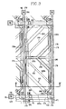
- Fig. 1 is a layout view of a thin film transistor (TFT) array panel for an LCD according to an embodiment of the invention.
- TFT thin film transistor
- Fig. 2 is a layout view of a color filter panel for an LCD according to an embodiment of the invention.
- Fig. 3 is a layout view of a red pixel of an LCD according to the embodiment shown in Fig. 1 and Fig. 2.
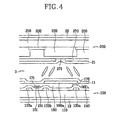
- Fig. 4 is a sectional view of the LCD shown in Fig. 3 taken along the line IV-IV'.
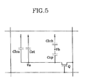
- Fig. 5 is a circuit diagram of the LCD shown in Figs. 1, 2, 3, and 4.
- Fig. 6 shows gamma curves relating to an LCD according to an embodiment of the invention.
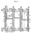
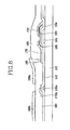
- Fig. 7 is a layout view of a TFT array panel for an LCD according to another embodiment of the invention.
- Fig. 8 is a sectional view of the TFT array panel shown in Fig. 7 taken along the line VIII-VIII'.
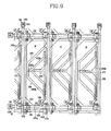
- Fig. 9 is a layout view of a TFT array panel for an LCD according to another embodiment of the invention.
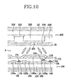
- Fig. 10 is a sectional view of an LCD including the TFT array panel shown in Fig. 9 taken along the line X-X',
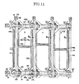
- Fig. 11 is a layout view of a TFT array panel for an LCD according to another embodiment of the invention.
- Fig. 12 is a sectional view of an LCD including the TFT array panel shown in Fig. 11 taken along the line XII - XII'.
- Fig. 1 is a layout view of a thin film transistor (TFT) array panel for an LCD according to an embodiment of the invention.
- Fig. 2 is a layout view of a color filter panel for an LCD according to an embodiment of the invention.
- Fig. 3 is a layout view of a red pixel of an LCD according to the embodiment shown in Fig. 1 and Fig. 2.
- Fig. 4 is a sectional view of the LCD shown in Fig. 3 taken along the line IV-IV'.
- an LCD includes a TFT array panel 100, a common electrode panel 200, and a LC layer 3 provided between the panels 100 and 200 and including a plurality of LC molecules aligned vertically with respect to surfaces of the panels 100 and 200.
- a structure of the TFT array panel 100 is described below.
- a plurality of first and second pixel electrodes 190a and 190b made of indium tin oxide (ITO) or indium zinc oxide (IZO) may be formed on an insulating substrate 110 made of a transparent material, such as glass.
- the first pixel electrode 190a is connected with a thin film transistor and receives image data voltages.
- the second pixel electrode 190b is overlaps with a coupling electrode 176 that is connected with the first pixel electrode 190a. Therefore, the second pixel electrode 190b is electrically coupled with the first pixel electrode 190a.
- the overlapping areas between the second pixel electrode 190b and the coupling electrode 176 are different among red, green, and blue pixels.
- a polarizer 12 is attached with the lower surface of the insulating substrate 110.
- the first and second pixel electrodes 190a and 190b may be made of a non-transparent material. It is understood that the polarizer 12 may be omitted when necessary.
- a structure of the color filter panel 200 is described below.
- a light blocking layer 220 to prevent light leakage, red, green, and blue color filters 230, and a common electrode 270 made of a transparent conductor, such as ITO or IZO are formed on an insulating substrate 210 made of a transparent material, such as glass.
- the common electrode 270 includes cutouts 271, 272, and 273.
- the light blocking layer 220 may be formed on areas overlapping the cutouts 271, 272, and 273, as well as near pixel areas to prevent light leakage due to the cutouts 271, 272, and 273.
- Alignment layers I and 21 are respectively formed on inner surfaces of the two panels 100 and 200 to align liquid crystal molecules.
- the alignment layers I 1 and 21 may vertically align the liquid crystal molecules with respect to the surfaces of the substrates 110 and 210; however, this is not necessary.
- the TFT array panel 100 is described below with reference to Figs. 1, 4, and 5.
- a plurality of gate lines 121 and a plurality of storage electrode lines 131 are formed on an insulating substrate 110.
- the gate lines 121 extend substantially in a transverse direction and each gate line 121 has a plurality of protruding gate electrodes 124, e.g., PROTRUSIONS, protruding along upper and lower side, and an expansion 129 or end portion for connecting to an external circuit.
- the expansion 129 may be wider than other portions of the gate line 121 except for the gate electrodes 124.
- the gate lines 121 transmit gate signals and extend substantially in a transverse direction.
- the expansion 129 of the gate lines 121 has an area that is sufficiently large for contact with another layer or an external driving circuit.
- a gate driving circuit (not shown) for generating the gate signals may be mounted or attached on a flexible printed circuit (FPC) film (not shown).
- the FPC may be attached with the substrate 110, directly mounted on the substrate 110, or integrated onto the substrate 110.
- the gate lines 121 may extend and connect with a driving circuit that may be integrated on the substrate 110.
- Each storage electrode line 131 extends substantially in the transverse direction and includes a plurality of sets of storage electrodes 133a, 133b, and 133c. Two storage electrodes 133a and 133b are extended substantially in a longitudinal direction and are connected with a transverse storage electrode 133c.
- the storage line 131 may include two or more transverse lines.
- the storage electrode line 131 may be provided at a substantially center portion of the two adjacent gate lines 121.
- the gate lines 12 and the storage electrode lines 131 may be made of an Al containing metal such as Al and Al alloy, an Ag containing metal such as Ag and Ag alloy, a Cu containing metal such as Cu and Cu alloy, a Mo containing metal such as Mo and Mo alloy, Cr, Ta, or Ti.
- the gate lines 121 may have a multi-layered structure including two conductive films (not shown) having different physical characteristics. One of the two films may be made of a low resistivity metal including the Al containing metal, the Ag containing metal, and the Cu containing metal for reducing signal delay or voltage drop.
- the other film may be made of material such as a Mo containing metal, a Cr containing metal, a Ta containing metal, or a Ti containing metal, which have good physical, chemical, and electrical contact characteristics with other materials such as indium tin oxide (ITO) or indium zinc oxide (IZO).
- ITO indium tin oxide
- IZO indium zinc oxide
- the gate lines 121 and the storage electrode lines 131 may be formed of various metal or conductor other than the above described materials.
- the lateral sides of the gate lines 121 and the storage electrode lines 131 are tapered or angled, and the inclination angle of the lateral sides with respect to a surface of the substrate 110 ranges between about 30 to about 80 degrees.
- a gate insulating layer 140 may be made of silicon nitride (SiNx) and is formed on the gate lines 121 and the storage electrode lines 131.
- a plurality of data lines 171, a plurality of drain electrodes 175, and a plurality of under-bridge metal pieces 172 are formed on the gate insulating layer 140.
- Each data line 171 extends substantially in the longitudinal direction and has a plurality of source electrodes 173 extending toward the drain electrodes 175.
- Each data line 171 includes an expansion 179 that may be wider than the data line so that the expansion 179 contacts another layer or an external device.
- the drain electrode 175 may extend to form a coupling electrode 176.
- the coupling electrode 176 may be bent to have a substantially "V" shape.
- the coupling electrodes 176 for the red, green, and blue pixels each have different lengths.
- the length of the coupling electrode 176 in the red (R) pixel may be the longest
- the length of the coupling electrode 176 in the blue (B) pixel may be the second longest
- the length of the coupling electrode 176 in the green (G) pixel may be the shortest.
- the under-bridge metal peaces 172 are disposed on the gate line 121 near the gate electrode 124.
- the data lines 171, drain electrodes 175, and the under-bridge metal pieces 172 may be made of a refractory metal such as Cr, Mo, Ta, Ti, or alloys thereof. However, they may have a multilayered structure including a refractory metal film (not shown) and a low resistivity film made of a metal such as an Al containing metal, an Ag containing metal, and a Cu containing metal.
- a plurality of semiconductor stripes 151 are formed under the data lines 171 and the drain electrodes 175 and the semiconductor stripes 15 and may extend substantially in a longitudinal direction.
- the semiconductor stripes 151 may be made of hydrogenated amorphous silicon (abbreviated to "a-Si") or polysilicon and have branches that extended toward the gate electrodes 124, the source electrodes 173, and the drain electrodes 175 to form channels 154 of TFTs.
- Ohmic contacts 161 and 165 may only be interposed between the underlying semiconductor stripes 151 and the overlying data conductors 171 and 175 thereon in order to reduce the contact resistance therebetween.
- the ohmic contact stripes and islands 161 and 165 may be made of n+ hydrogenated a-Si heavily doped with an n-type impurity such as phosphorous or they may be made of silicide.
- Each ohmic contact stripe 161 has a plurality of projections 163. The projections 163 and the ohmic contact islands 165 may be located in pairs on the projections 154 of the semiconductor stripes 151.
- a passivation layer 180 made of an organic material having photosensitivity and having a good planarization characteristic, a low dielectric material such as a-Si:C:O, a-Si:O:F which are formed by plasma enhanced chemical vapor deposition (PECVD), or an inorganic material such as silicon nitride may be formed on the data lines 171, the drain electrodes 175, and the under-bridge metal piece 172.
- the passivation layer 180 may be a single layer formed one of such materials or be multiple layers formed by combining such materials.
- the passivation layer 180 may includes a bottom layer of SiNx and a top layer of an organic material, or vice-versa.
- the passivation layer 180 includes a plurality of contact holes 185 and 182 exposing a portion of the drain electrode 175 and the expansion 179 of the data line 171, respectively.
- the passivation layer 180 and the gate insulating layer 140 include a plurality of contact holes 181, 184, and 183 exposing the expansion 129 of the gate line 121 and two portions of the storage electrode line 131, respectively.
- a plurality of pixel electrodes 190, a plurality of contact assistants 81 and 82, and storage bridges 84 are formed on the passivation layer 180. They may be made of a transparent conductive material such as ITO or IZO or reflective and conductive material such as Ag, Al, or alloys thereof.
- Each pixel electrode 190 includes a first sub-pixel electrode 190a and a second sub-pixel electrode 190b.
- the first sub-pixel electrode 190a is connected with, e.g., coupled, the drain electrode 175 through the contact hole 185.
- the second sub-pixel electrode 190b is electrically floated and capacitively coupled with the first sub-pixel electrode 190a.
- the coupling capacitances formed between the first sub-pixel electrode 190a and the second sub-pixel electrode 190b are different among the green, red, and blue pixels.
- the coupling capacitances formed between the first sub-pixel electrode 190a and the second sub-pixel electrode 190b decrease in the following order due to the length shortening of the coupling electrodes 176: red (R), blue (B), and green (G) pixels.
- the coupling capacitances of the first sub-pixel electrode 190a and the second sub-pixel electrode 190b among green, red, and blue pixel may be made different according to other methods, such as width and positional differentiation of the coupling electrode 176, rather than by length differentiation. In any case, overlapping area between the coupling electrode 176 and the second sub-pixel electrode 190b determines the capacitance of the coupling capacitor and the capacitance increases along with increase of the overlapping area.
- Cutouts 191, 193, and 194 dividing the first sub-pixel electrode 190a and the second sub-pixel electrode 190b may be classified into oblique portions 191 and 193 forming an angle of about 45 degrees with the gate line 121, and a longitudinal portion 194 making an angle of about 90 degrees with the gate line 121.
- the two oblique portions 191 and 193 together form an angle of about 90 degrees.
- the second sub-pixel electrode 190b has a cutout 192 which initiates from the right side of the second sub-pixel electrode 190b and extends toward the left side.
- the entrance of the cutout 191 widens due to the corner cut of the second sub-pixel electrode 190b.
- the first sub-pixel electrode 190a and the second sub-pixel electrode 190b respectively are substantially symmetrical about a longitudinal center line of a pixel.
- the storage bridge 84 crosses over the gate line 121 and connects two storage lines that are disposed on each side of the gate line 121.
- the storage bridge 84 makes contact with the storage electrode 133a and the storage electrode line 131 through the contact holes 183 and 184.
- the storage bridge 84 overlaps the under-bridge metal piece 172.
- the storage bridge 84 electrically connects each of the storage electrode lines 131 on the insulating substrate 110.
- the storage electrode lines 13 may be used to repair defects of the gate lines 121 and the data lines 171. Such repairs may be performed using a laser.
- the under-bridge metal piece 172 provides electrical connection of the gate line 121 and the storage bridge 84.
- the contact assistants 81 and 82 are respectively connected with the expansion 129 of the gate line 121 and the expansion 179 of the data line 171 through the contact holes 181 and 182.
- a light blocking member 220 referred to as a black matrix, for preventing light leakage is formed on an insulating substrate 210.
- the light blocking member 220 may have a plurality of openings that face the pixel electrodes 190 and it may have substantially the same planar shape as the pixel electrodes 190.
- a plurality of color filters 230 are also formed on the substrate 210 and they are disposed substantially in the areas enclosed by the light blocking member 220 and may overlap edge portions of the light blocking member 220.
- the color filters 230 may extend substantially along the longitudinal direction along the pixel electrodes 190.
- the color filters 230 may represent one of the primary colors such as red, green, and blue colors.
- An overcoat 250 is formed on the color filters 230 and the light blocking member 220.
- the overcoat 250 is may be made of (organic) insulator and it prevents the color filters 230 from being exposed and provides a substantially flat surface.
- a common electrode 270 is formed on the overcoat 250.
- the common electrode 270 may be made of a transparent conductive material such as ITO and IZO and has a plurality of sets of cutouts 271, 272, and 273.
- a set of cutouts 271, 272, and 273 include oblique portions and end portions.
- the oblique portions of the cutouts 271, 272, and 273 are substantially parallel with the oblique portions 191 and 193 of the cutout between the pixel electrodes 190a and 190b.
- the oblique portions 191 and 193 are disposed between the oblique portions of the cutouts 271, 272, and 273.
- the end portions overlap with the boundary line of the pixel area and include substantially longitudinal end portions and substantially transverse end portions.
- the LCD includes a TFT array panel 100, a color filter array panel 200 facing the TFT array panel 100 and separated therefrom by a predetermined space, and a liquid crystal layer 3 filled or provided in the predetermined space.
- the cutouts 271, 272, and 273 of the common electrode 270 divide the two sub-pixel electrodes 194a and 190b into a plurality of sub-areas.
- the two sub-pixels 190a and 190b are respectively divided into four sub-areas.
- each sub-area has two parallel long edges and several short edges. Therefore, the sub-areas have length direction and width direction.
- Each liquid crystal 3 portion disposed between each of the sub-areas of the pixel electrodes 190 and corresponding sub-areas of the common electrode 270 is referred to as a subregion.
- the sub-regions are classified into four species according to the average long axis direction of liquid crystals disposed therein.
- the sub-regions are referred to as a domain hereinbelow.
- the first sub-pixel electrode 190a is physically and electrically coupled or connected with the drain electrodes 175 through the contact holes 181.
- the second sub-pixel electrode 190b is physically and electrically floated and overlaps with the coupling electrode 176 to form coupling capacitances with the first sub-pixel electrodes 190a. Therefore, the voltage of the second sub-pixel electrode 190b depends on the voltage of the first sub-pixel electrode 190a.
- the voltage of the second sub-pixel electrode 190b with respect to the common voltage is always smaller than that the voltage of the first sub-pixel electrode 190a.
- a pixel area When a pixel area includes two sub-areas with different electric fields, lateral visibility is improved by the mutual compensation in the two sub-areas.
- the coupling relationship between the first sub-pixel electrode 190a and the second sub-pixel electrode 190b is described below with reference to Fig. 5.
- Fig. 5 is a circuit diagram of the LCD shown in Figs. 1, 2, 3, and 4.
- Clca refers to a liquid crystal (LC) capacitance formed between the first sub-pixel electrode 190a and the common electrode 270.
- Cst refers to a storage capacitance formed between the first sub-pixel electrode 190a and the storage line 131.
- Clcb refers to a liquid crystal (LC) capacitance formed between the second sub-pixel electrode 190b and the common electrode 270.
- Ccp refers to a coupling capacitance formed between the first sub-pixel electrode 190a and the second sub-pixel electrode 190b.
- Vb is necessarily less than Va.
- the capacitance Ccp may be adjusted by overlapping an area or changing a distance between the second sub-pixel electrode 190b and the coupling electrode 176.
- the overlapping area between the second sub-pixel electrode 190b and the coupling electrode 176 may be adjusted by changing the width of the coupling electrode 176.
- the distance between the second sub-pixel electrode 190b and the coupling electrode 176 may be adjusted by changing a location of the coupling electrode 176. That is, in the present embodiment, the coupling electrode 176 is formed on the same layer as the data line 171; however, it is understood that various other structures may be applied.
- a coupling assistant electrode (not shown) coupled with the second sub-pixel electrode 190b may be formed on the same layer as the gate line 121 and the coupling assistant electrode may be capacitively coupled with the coupling electrode 176 to apply voltages to the second sub-pixel electrode 190b.
- the gate insulating layer 140 interposed between the coupling electrode 176 and the coupling assistant electrode is the main dielectric of coupling capacitor.
- This structure may be applied when the passivation layer 180 is made of a thick organic material having a low dielectric constant, thereby coupling capacitance formed by the passivation layer 180 is not sufficient.
- these structures may be combined to use both the gate insulating layer 140 and the passivation layer 180 as dielectric of the coupling capacitor.
- voltage differences or transmittances between the two sub-pixel electrodes 190a and 190b are different among red, green, and blue pixels due to the difference of coupling capacitance and/or due to the different ratio of area for the two sub-pixel electrodes 190a and 190b. Accordingly, a color reproduction property of the LCD with respect to a memory color at any viewing direction is improved and high transmittance of pixels is maintained.
- the memory color refers to color memorized or recognized by the human brain. When visibility with respect to the memory color is degraded at a lateral view as compared with a front view, display quality deteriorates.
- Fig. 6 shows gamma curves relating to an LCD of the present invention.
- the solid line (a) is a gamma curve measured at the front where the viewing angle is 0 and the dashed line (b) is a gamma curve measured at a lateral angle of an LCD having pixels which are not split.
- the bold solid line (c) and bold dashed line (d) are gamma curves measured at a lateral angle of an LCD having pixels that are split, e.g., each pixel having two sub-pixel electrodes having different voltages. Voltage ratios of the two sub-pixel electrodes are different between the bold solid line (c) and the bold dashed line (d).
- the lateral angle gamma curve (b) measured at a viewing angle for example 60 degrees
- the lateral angle gamma curve (b) significantly distorts.
- the lateral angle gamma curves (c, d) are improved to more closely resemble the front gamma curve (a). Accordingly, the viewing angle increases, thereby improving lateral visibility.
- Region A is a low gray voltage region (dark region). Lateral angle gamma curve of region A is substantially determined by a sub-pixel electrode capacitively that is coupled with a sub-pixel electrode connected with a TFT.
- Region B is a high gray voltage region (bright region). Lateral angle gamma curve of region B is substantially determined by the sub-pixel electrode connected with the TFT. Here, the gradient of the gamma curve (arrow mark of diagonal direction) is determined by a ratio of the voltage that is applied to the two sub-pixel electrodes. The position (arrow mark of horizontal direction) of boundary of regions A and B may be determined by a ratio of area the two sub-pixel electrodes.
- area ratio or voltage ratio between the two sub-pixel electrodes 190a and 190b was adjusted to make a color tone according to the lateral view nearly to coincide with a color tone of the front view with respect to skin color which is one of the memory colors.
- the adjustment took into consideration that a voltage ratio of the second sub-pixel electrode 190b with respect to the first sub-pixel electrode 190a in a green pixel and a blue pixel is preferably smaller than a voltage ratio of the second sub-pixel electrode 190b with respect to the first sub-pixel electrode 190a in a red pixel. Additionally, it is even more preferable that the voltage ratio of the second sub-pixel electrode 190b with respect to the first sub-pixel electrode 190a decreases in an order of red, blue and green pixels.
- the skin color series generally consists of red, green and blue colors in an amount such that the proportion of red light is greater than green light and the proportion of green light is greater than blue light (> green > blue).
- the color tone is distorted and the proportions of the green light and the blue light are increased with respect to the red light.
- the skin color series includes 50% of red light, 20-30% of green light, and 10-20% of blue light.
- a ratio of a lateral transmittance with respect to a front transmittance increases.
- the proportion of red, green, and blue in the front view is 50:20:10
- the proportion of red, green, and blue in a lateral view is change to be 60:40:30. This change degrades the color tone in a lateral view. Accordingly, adjustment of gamma curve with respect to red, green, and blue pixel is necessary.
- the voltage ratios of respective pixels are shown below in Table 1.
- Table 1 and Table 2 show experimental data for calculating the most appropriate voltage ratio in red pixels.
- Table 1 includes data for lateral transmittance values and front transmittance values measured while the voltage ratio is varied from 0.800 to 0.600 and gray level is 196.
- Table 2 shows a difference of the transmittance ratio between the lateral and the front transmittance values calculated from Table 1.
- the transmittance ratio of lateral/front transmittance is enlarged in red pixels.
- the transmittance ratio between the lateral transmittance and the front transmittance is substantially uniform in red pixels.
- the front transmittance may also decrease. Accordingly, when the lateral angle visibility and the front transmittance are both considered, it is preferable that the voltage ratio is determined in a range between about 0.675 and about 0.800, which is a relatively high voltage range. In the present embodiment, 0.700 is determined to be the most appropriate voltage ratio for red pixels.
- Table 3 and Table 4 show experimental data for calculating the most appropriate voltage ratio in green pixels.
- Table 3 includes lateral transmittance values and front transmittance values measured while the voltage ratio is varied from 0.800 to 0.600 and a gray level is 124.
- Table 4 shows a difference of a transmittance ratio between the lateral and the front transmittance values calculated from Table 3.
- the transmittance ratio of lateral/front transmittance is reduced in green pixels.
- the lateral viewing angle improves when the voltage ratio of the green pixels decreases. However, if the voltage ratio decreases too much, the transmittance at the front may also decrease.
- the variation of transmittance ratio between the lateral and front transmittance, which is induced by varying the voltage ratio, is large in green pixels.
- the variation of transmittance ratio is saturated at voltage ratio of about 0.600-0.650, which differs from the red pixels.
- 0.625 is determined to be the most appropriate voltage ratio for green pixels.
- Table 5 and Table 6 show data of experiment to calculate the most appropriate voltage ratio in blue pixels.
- Table 5 includes lateral transmittance values and front transmittance values measured while the voltage ratio is varied from 0.800 to 0.600 and a gray level is 96.
- Table 6 shows a difference of a transmittance ratio between the lateral and the front transmittance values calculated from Table 5.
- the transmittance ratio of the lateral/front transmittance is reduced in blue pixels.
- lateral visibility increases as the voltage ratio of blue pixels decreases. However, if the voltage ratio decreases too much, the transmittance at the front may also decrease.
- the variation of a transmittance ratio between the lateral and front transmittance, which is induced by varying voltage ratio, is large in blue pixels.
- the variation of transmittance ratio is saturated at voltage ratio of about 0.650 to 0.700, which is different from red pixels.
- 0.675 is determined to be the most appropriate voltage ratio for blue pixels.
- Table 7 shows improvement of lateral visibility achieved by applying the most appropriate voltage ratios to the respective red, green, and blue pixels.
- Table 7 Vw 14.0V 14.5V 14.5V 14.5V Device 40.0"W2 17.0"E6 17.0"E6 17,0"E6 Area Ratio 1:1 1.45:1 1.45: 1.45:1 Voltage Ratio (R:G:B) 0.75:0.75:0.75 0.7:0.7:0.7 0.7:0.625:0675 0.7:0.7:0.6 ⁇ u'v' SONY Left: 0.02 Left: 0.0107 Left: 0.0055 Left: 0.0161 At lateral 60 degrees Skin Right: 0.021 Right: 0.0174 Right: 0.0106 Right: 0.0216 Light Skin Left: 0.0130 Left: 0.0067 Left: 0.0071 Left: 0.0128 Right:0.0154 Right: 0.0116 Right: 0.0125 Right:0.0141 Pale Left: 0.0173 Left:0.0101 Left: 0.0050 Left: 0.0142 Orange Right:0.0177 Right: 0.0159 Right: 0.0120
- ⁇ u'v' of Table 7 represents difference of two colors in the color coordinate of International Commission on Illumination (CIE).
- CIE International Commission on Illumination
- the area ratio of the second sub-pixel electrode 190b versus the first sub-pixel electrode 190a is 1:1.5.
- the present invention may be applied to other area ratios.
- Table 8 contains front transmittance and lateral transmittance according to variation of the voltage ratio when the area ratio of the two sub-pixels is 1:1.
- Table 9 contains front transmittance and lateral transmittance according to variation of the voltage ratio when the area ratio of the two sub-pixels is 1:2.
- Table 10 summarizes the above descriptions.
- Table 10 Area Ratio (MAIN : SUB) 1:1 1:1.5 1:2 Note RED 0.725 0.70 0.675 As area ratio of sub-pixel electrodes increases, voltage ratio is required to be reduced for enhancing visibility of skin colors.
- MAIN represents the first sub-pixel electrode 190a and SUB represents the second sub-pixel electrode 190b.
- the voltage ratios of green pixels are about 0.075 less than that the voltage ratios of red pixels and the voltage ratio of blue pixels are about 0.025 less than that the voltage ratios of blue pixels.
- Brightness may be enhanced by increasing an area of the first sub-pixel which is directly connected with the TFT and has a relatively high brightness and reducing an area of the second sub-pixel which is capacitively coupled with the first sub-pixel and has a relatively low brightness.
- the first sub-pixel and second sub-pixel are disposed in a pixel representing a color highly contributing to the brightness.
- the present invention may be applied to a TN(twisted nematic) LCD. Another embodiment having this feature is described below with reference to the drawings.
- Fig. 7 is a layout view of a TFT array panel for an LCD according to another embodiment of the invention.
- Fig. 8 is a sectional view of the TFT array panel shown in Fig. 7 taken along the line VIII-VIII'.
- Layered structures of the TFT panel 100 according to this embodiment are substantially the same as those shown in Figs. 1, 3 and 4.
- a plurality of gate lines 121 including gate electrodes 124 and end portions 129, a plurality of storage electrode lines 131 including storage electrodes 133a, 133b, and 133c may be formed on a substrate 110.
- a gate insulating layer 140, a plurality of semiconductor stripes 151 having projections 154, and a plurality of ohmic contacts 161 and 165 may be sequentially formed on the gate lines 121 and the storage electrodes lines 131.
- a plurality of data lines 171 including source electrodes 173 and end portions 179, a plurality of drain electrodes 175 including coupling electrodes 176, and a plurality of metal pieces 172 may be formed on the ohmic contacts 161 and 165.
- a passivation layer 180 may be formed on the data lines 171, the drain electrodes 175, and exposed portions of the semiconductor stripes 151.
- a plurality of contact holes 181-185 may be provided at the passivation layer 180 and the gate insulating layer 140.
- a plurality of pixel electrodes 190 including sub-pixel electrodes 190a and 190b, a plurality of storage bridges 84, and a plurality of contact assistants 81 and 82 may be formed on the passivation layer 180.
- position of the transverse storage electrodes 133c is different according to red (R), green (G) and blue (B) pixels.
- the transverse storage electrode 133c of green pixel is disposed at the most upper portion of the pixel area
- the transverse storage electrode 133c of red pixel is disposed at the second most upper portion of the pixel area
- the transverse storage electrode 133c of blue pixel is disposed at the third most upper portion of the pixel area.
- the first sub-pixel electrode 190a and the second sub-pixel electrode 190b are divided into upper and lower on the transverse storage electrode 133c, respectively.
- the coupling electrode 176 extends along the storage electrodes 133a, 133b, and 133c and overlaps the storage electrodes 133a, 133b, and 133e.
- the coupling electrode 176 includes substantially longitudinal portions 176a and 176c respectively overlapping the storage electrodes 133a and 133b and a substantially transverse portion 133c overlapping the storage electrode 133c.
- Widths (W R , W G , W B ) of the coupling electrodes 176 are different according to the red (R), the green (G), and the blue (B) pixels. Accordingly, overlapping areas between the coupling electrodes 176 and the second sub-pixel electrodes 190b are different according to the red (R), the green (G), and the blue (B) pixels.
- coupling capacitances between the first sub-pixel electrodes 190a and the second sub-pixel electrodes 190b are different according to the red (R), the green (G), and the blue (B) pixels.
- voltage ratios of the second sub-pixel electrode 190b with respect to the first sub-pixel electrode 190a are different according to the red (R), the green (G), and the blue (B) pixels.
- Area ratios of the first sub-pixel electrodes 190a versus the second sub-pixel electrodes 190b are also different according to the red (R), the green (G), and the blue (B) pixels. These voltage ratio and area ratio may be adjusted to improve visibility and transmittance.
- Fig. 9 is a layout view of a TFT array panel for an LCD according to another embodiment of the invention.
- Fig. 10 is a sectional view of an LCD including the TFT array panel shown in Fig. 9 taken along the line X-X'.
- layered structures of the TFT panel 100 are substantially the same as those shown in Figs. 1, 3 and 4 except for some features described below.
- a plurality of gate lines 121 including gate electrodes 124 and end portions 129, a plurality of storage electrode lines 131 including storage electrodes 133a, 133b, and 133c may be formed on a substrate 110.
- a gate insulating layer 140, a plurality of semiconductor stripes 151 having projections 154, and a plurality of ohmic contacts 161 and 165 may be sequentially formed on the gate lines 121 and the storage electrodes lines 131.
- a plurality of data lines 171 including source electrodes 173 and end portions 179, a plurality of drain electrodes 175 including coupling electrodes 176, and a plurality of metal pieces 172 may be formed on the ohmic contacts 161 and 165.
- a passivation layer 180 may be formed on the data lines 171, the drain electrodes 175, and exposed portions of the semiconductor stripes 151.
- a plurality of contact holes 181-185 may be provided at the passivation layer 180 and the gate insulating layer 140.
- a plurality of pixel electrodes 190 including sub-pixel electrodes 190a and 190b, a plurality of storage bridges 84 and a plurality of contact assistants 81 and 82 may be formed on the passivation layer 180.
- the semiconductor stripes 151 have substantially the same planar shapes as the data lines 171, the drain electrodes 175, and the underlying ohmic contacts 161 and 165. However, the semiconductor stripes 151 include some exposed portions, which are not covered with the data lines 171 and the drain electrodes 175, such as portions located between the source electrodes 173 and the drain electrodes 175.
- area ratios of the first sub-pixel electrodes 190a versus the second sub-pixel electrodes 190b are different according to the red (R), the green (G), and the blue (B) pixels.
- Area ratio of the second sub-pixel electrode 190b with respect to the first sub-pixel electrode 190a is preferably larger in red pixel than in green pixels or blue pixels. It is preferable that a ratio of an area of the second sub-pixel electrode 190b with respect to an area of the first sub-pixel electrode 190a decreases in an order of red, blue and green pixels.
- the TFT array panel for an LCD has coupling electrodes 176, amorphous silicon layers 154, and ohmic contact layers 165 that are formed under the coupling electrodes 176 with substantially the same shape.
- a photoresist layer having different thicknesses according to positions is used.
- Fig. 11 is a layout view of a TFT array panel for an LCD according to another embodiment of the invention.
- Fig. 12 is a sectional view of an LCD including the TFT array panel shown in Fig. 11 taken along the line XII-XII'.
- layered structures of the TFT panel 100 according to this embodiment are substantially the same as those shown in Fig. 7 and Fig. 8.
- the semiconductor stripes 151 have substantially the same planar shapes as the data lines I71, the drain electrodes 175, and the underlying ohmic contacts 161 and 165. However, the semiconductor stripes 151 include exposed portions, which are not covered with the data lines 171 and the drain electrodes 175, such as portions located between the source electrodes 173 and the drain electrodes 175.
- an LCD displays a lateral angle color tone that is substantially the same as a front color tone and has a high transmittance.
- cutouts in the pixel and common electrodes may be rearranged in various ways and shapes.
Abstract
Description
- This application claims priority to and the benefit of
Korean Patent Application No. 10-2004-0061397, filed on August 4, 2004 Korean Patent Application No. 10-2005-0013458 filed on February 18, 2005 - The present invention relates to a liquid crystal display and a thin film transistor array panel.
- A liquid crystal display (LCD) is a common type of flat panel display. An LCD includes two panels provided with field-generating electrodes, and a liquid crystal (LC) layer interposed therebetween. The LCD displays images by applying voltages to the field-generating electrodes to generate an electric field in the LC layer, which changes orientations of LC molecules in the LC layer to adjust polarization of incident light.
- A disadvantage of the LCD is that it has a relatively narrow viewing angle. Various techniques for enlarging the viewing angle have been suggested, such as utilizing a vertically aligned LC and providing cutouts or protrusions at field-generating electrodes such as pixel electrodes and a common electrode.
- For example, when the pixel electrodes and a common electrode respectively have cutouts, the cutouts induce a slanted electric field, and the slanted electric field controls falling directions of liquid crystals. Control of the falling direction of liquid crystals makes it possible to widen the viewing angle of liquid crystal display.
- For example, when the pixel electrodes and the common electrode respectively have protrusions, the protrusions are formed on both of pixel electrodes and a common electrode, the protrusions induce a slanted electric field, and the slanted electric field controls falling directions of liquid crystals.
- Additional methods in which pixel electrodes have cutouts and protrusions formed on a common electrode may be used to control falling directions of liquid crystals.
- An LCD using cutouts or protrusions has a viewing angle of greater than approximately 80 degrees in any direction, which has an improved contrast ratio in view of a standard contrast ratio of 1:10, and in view of gray scale inversion where a viewing angle of occurring brightness inversion is a standard angle. However, such an LCD shows poor visibility that is inferior to a twisted nematic mode LCD. The poor visibility is caused by discordance of the gamma curve between the front view and lateral view.
- For example, in a vertically aligned mode LCD using cutouts, as the viewing angle increases, the picture plane becomes brighter and the color shifts toward white. When this phenomenon is excessive, the image distorts because the brightness difference between gray scales disappears.
- The present invention provides an LCD having a high transmittance ratio and a small difference in color tone between a front view and a lateral view.
- Additional features of the invention will be set forth in the description which follows, and in part will be apparent from the description, or may be learned by practice of the invention.
- The present invention discloses a liquid crystal display, including an insulating substrate; a plurality of first signal lines formed on the insulating substrate; a plurality of second signal lines crossing the first signal lines and insulated from the first signal lines; a plurality of thin film transistors coupled with the first signal lines and the second signal lines; and a plurality of pixels including a plurality of first sub-pixel electrodes coupled with the thin film transistors and a plurality of second sub-pixel electrodes capacitively coupled with the first sub-pixel electrodes, wherein a voltage ratio of the second sub-pixel electrode with respect to the first sub-pixel electrode has at least two different values.
- The present invention also discloses a thin film transistor array panel, including an insulating substrate; a plurality of first signal lines formed on the insulating substrate; a plurality of second signal lines crossing the first signal lines and insulated from the first signal lines; a plurality of thin film transistors coupled with the first signal lines and the second signal lines; and a plurality of pixels including a plurality of first sub-pixel electrodes coupled with the thin film transistors, a plurality of coupling electrodes coupled with the thin film transistors, and a plurality of second sub-pixel electrodes overlapping the coupling electrodes, wherein an overlapping area of the coupling electrodes and the second sub-pixel electrodes has at least two different values.
- The present invention also discloses a liquid crystal display, including an insulating substrate; a plurality of first signal lines formed on the insulating substrate; a plurality of second signal lines crossing the first signal lines and insulated from the first signal lines; a plurality of thin film transistors coupled with the first signal lines and the second signal lines; and a plurality of pixels including a plurality of first sub-pixel electrodes coupled with the thin film transistors and a plurality of second sub-pixel electrodes capacitively coupled with the first sub-pixel electrodes, wherein the pixels include a red pixel, a green pixel, and a blue pixel and a voltage ratio of the second sub-pixel electrode with respect to the first sub-pixel electrode is different among the red pixel, the green pixel, and the blue pixel so that a brightness ratio of the red component, the green component, and the blue component at a lateral position in a gray level is nearer to a brightness ratio of the red component, the green component, and the blue component at a front position in the gray level as compared with not having different voltage ratios among the red pixel, the green pixel, and the blue pixel.
- The present invention also discloses a liquid crystal display, including n insulating substrate; a plurality of first signal lines formed on the insulating substrate; a plurality of second signal lines crossing the first signal lines and insulated from the first signal lines; a plurality of thin film transistors coupled with the first signal lines and the second signal lines; and a plurality of pixels including a plurality of first sub-pixel electrodes coupled with the thin film transistors and a plurality of second sub-pixel electrodes capacitively coupled with the first sub-pixel electrodes, wherein a ratio of an area of the second sub-pixel electrode with respect to an area of the first sub-pixel electrode has at least two different values.
- It is to be understood that both the foregoing general description and the following detailed description are exemplary and explanatory and are intended to provide further explanation of the invention as claimed.
- The accompanying drawings, which are included to provide a further understanding of the invention and are incorporated in and constitute a part of this specification, illustrate embodiments of the invention and together with the description serve to explain the principles of the invention.
- Fig. 1 is a layout view of a thin film transistor (TFT) array panel for an LCD according to an embodiment of the invention.
- Fig. 2 is a layout view of a color filter panel for an LCD according to an embodiment of the invention.
- Fig. 3 is a layout view of a red pixel of an LCD according to the embodiment shown in Fig. 1 and Fig. 2.
- Fig. 4 is a sectional view of the LCD shown in Fig. 3 taken along the line IV-IV'.
- Fig. 5 is a circuit diagram of the LCD shown in Figs. 1, 2, 3, and 4.
- Fig. 6 shows gamma curves relating to an LCD according to an embodiment of the invention.
- Fig. 7 is a layout view of a TFT array panel for an LCD according to another embodiment of the invention.
- Fig. 8 is a sectional view of the TFT array panel shown in Fig. 7 taken along the line VIII-VIII'.
- Fig. 9 is a layout view of a TFT array panel for an LCD according to another embodiment of the invention.
- Fig. 10 is a sectional view of an LCD including the TFT array panel shown in Fig. 9 taken along the line X-X',
- Fig. 11 is a layout view of a TFT array panel for an LCD according to another embodiment of the invention.
- Fig. 12 is a sectional view of an LCD including the TFT array panel shown in Fig. 11 taken along the line XII-XII'.
- The present invention is described more fully below with reference to the accompanying drawings, in which preferred embodiments of the invention are shown. The present invention may, however, be embodied in many different forms and should not be construed as being limited to the embodiments set forth herein.
- In the drawings, the thickness of layers, films, and regions are exaggerated for clarity. Like numerals refer to like elements throughout. It is understood that when an element such as a layer, film, region, or substrate is referred to as being "on" another element, the element can be directly on the other element or intervening elements may also be present. In contrast, when an element is referred to as being "directly on" another element, there are no intervening elements present.
- Liquid crystal displays and thin film transistor (TFT) array panels for LCDs according to embodiments of the invention are described below with reference to the accompanying drawings.
- Fig. 1 is a layout view of a thin film transistor (TFT) array panel for an LCD according to an embodiment of the invention. Fig. 2 is a layout view of a color filter panel for an LCD according to an embodiment of the invention. Fig. 3 is a layout view of a red pixel of an LCD according to the embodiment shown in Fig. 1 and Fig. 2. Fig. 4 is a sectional view of the LCD shown in Fig. 3 taken along the line IV-IV'.
- According to an embodiment of the invention, an LCD includes a
TFT array panel 100, acommon electrode panel 200, and aLC layer 3 provided between thepanels panels - A structure of the
TFT array panel 100 is described below. - A plurality of first and
second pixel electrodes insulating substrate 110 made of a transparent material, such as glass. Thefirst pixel electrode 190a is connected with a thin film transistor and receives image data voltages. Thesecond pixel electrode 190b is overlaps with acoupling electrode 176 that is connected with thefirst pixel electrode 190a. Therefore, thesecond pixel electrode 190b is electrically coupled with thefirst pixel electrode 190a. - The overlapping areas between the
second pixel electrode 190b and thecoupling electrode 176 are different among red, green, and blue pixels. - A
polarizer 12 is attached with the lower surface of theinsulating substrate 110. When a reflective LCD is considered, the first andsecond pixel electrodes polarizer 12 may be omitted when necessary. - A structure of the
color filter panel 200 is described below. - A
light blocking layer 220 to prevent light leakage, red, green, andblue color filters 230, and acommon electrode 270 made of a transparent conductor, such as ITO or IZO are formed on aninsulating substrate 210 made of a transparent material, such as glass. - The
common electrode 270 includescutouts light blocking layer 220 may be formed on areas overlapping thecutouts cutouts - Alignment layers I and 21 are respectively formed on inner surfaces of the two
panels substrates - The
TFT array panel 100 is described below with reference to Figs. 1, 4, and 5. - A plurality of gate lines 121 and a plurality of
storage electrode lines 131 are formed on an insulatingsubstrate 110. - The gate lines 121 extend substantially in a transverse direction and each gate line 121 has a plurality of protruding
gate electrodes 124, e.g., PROTRUSIONS, protruding along upper and lower side, and anexpansion 129 or end portion for connecting to an external circuit. Theexpansion 129 may be wider than other portions of the gate line 121 except for thegate electrodes 124. - The gate lines 121 transmit gate signals and extend substantially in a transverse direction. The
expansion 129 of the gate lines 121 has an area that is sufficiently large for contact with another layer or an external driving circuit. A gate driving circuit (not shown) for generating the gate signals may be mounted or attached on a flexible printed circuit (FPC) film (not shown). The FPC may be attached with thesubstrate 110, directly mounted on thesubstrate 110, or integrated onto thesubstrate 110. The gate lines 121 may extend and connect with a driving circuit that may be integrated on thesubstrate 110. - Each
storage electrode line 131 extends substantially in the transverse direction and includes a plurality of sets ofstorage electrodes storage electrodes transverse storage electrode 133c. Thestorage line 131 may include two or more transverse lines. Thestorage electrode line 131 may be provided at a substantially center portion of the two adjacent gate lines 121. - The gate lines 12 and the
storage electrode lines 131 may be made of an Al containing metal such as Al and Al alloy, an Ag containing metal such as Ag and Ag alloy, a Cu containing metal such as Cu and Cu alloy, a Mo containing metal such as Mo and Mo alloy, Cr, Ta, or Ti. The gate lines 121 may have a multi-layered structure including two conductive films (not shown) having different physical characteristics. One of the two films may be made of a low resistivity metal including the Al containing metal, the Ag containing metal, and the Cu containing metal for reducing signal delay or voltage drop. The other film may be made of material such as a Mo containing metal, a Cr containing metal, a Ta containing metal, or a Ti containing metal, which have good physical, chemical, and electrical contact characteristics with other materials such as indium tin oxide (ITO) or indium zinc oxide (IZO). The gate lines 121 and thestorage electrode lines 131 may be formed of various metal or conductor other than the above described materials. - The lateral sides of the gate lines 121 and the
storage electrode lines 131 are tapered or angled, and the inclination angle of the lateral sides with respect to a surface of thesubstrate 110 ranges between about 30 to about 80 degrees. - A
gate insulating layer 140 may be made of silicon nitride (SiNx) and is formed on the gate lines 121 and the storage electrode lines 131. - A plurality of
data lines 171, a plurality ofdrain electrodes 175, and a plurality of under-bridge metal pieces 172 are formed on thegate insulating layer 140. - Each
data line 171 extends substantially in the longitudinal direction and has a plurality ofsource electrodes 173 extending toward thedrain electrodes 175. - Each
data line 171 includes anexpansion 179 that may be wider than the data line so that theexpansion 179 contacts another layer or an external device. - The
drain electrode 175 may extend to form acoupling electrode 176. Thecoupling electrode 176 may be bent to have a substantially "V" shape. Thecoupling electrodes 176 for the red, green, and blue pixels each have different lengths. The length of thecoupling electrode 176 in the red (R) pixel may be the longest, the length of thecoupling electrode 176 in the blue (B) pixel may be the second longest, and the length of thecoupling electrode 176 in the green (G) pixel may be the shortest. - The under-
bridge metal peaces 172 are disposed on the gate line 121 near thegate electrode 124. - The data lines 171,
drain electrodes 175, and the under-bridge metal pieces 172 may be made of a refractory metal such as Cr, Mo, Ta, Ti, or alloys thereof. However, they may have a multilayered structure including a refractory metal film (not shown) and a low resistivity film made of a metal such as an Al containing metal, an Ag containing metal, and a Cu containing metal. - A plurality of
semiconductor stripes 151 are formed under thedata lines 171 and thedrain electrodes 175 and the semiconductor stripes 15 and may extend substantially in a longitudinal direction. Thesemiconductor stripes 151 may be made of hydrogenated amorphous silicon (abbreviated to "a-Si") or polysilicon and have branches that extended toward thegate electrodes 124, thesource electrodes 173, and thedrain electrodes 175 to formchannels 154 of TFTs. -
Ohmic contacts underlying semiconductor stripes 151 and theoverlying data conductors islands ohmic contact stripe 161 has a plurality ofprojections 163. Theprojections 163 and theohmic contact islands 165 may be located in pairs on theprojections 154 of thesemiconductor stripes 151. - A
passivation layer 180 made of an organic material having photosensitivity and having a good planarization characteristic, a low dielectric material such as a-Si:C:O, a-Si:O:F which are formed by plasma enhanced chemical vapor deposition (PECVD), or an inorganic material such as silicon nitride may be formed on thedata lines 171, thedrain electrodes 175, and the under-bridge metal piece 172. Thepassivation layer 180 may be a single layer formed one of such materials or be multiple layers formed by combining such materials. For example, thepassivation layer 180 may includes a bottom layer of SiNx and a top layer of an organic material, or vice-versa. - The
passivation layer 180 includes a plurality ofcontact holes drain electrode 175 and theexpansion 179 of thedata line 171, respectively. Thepassivation layer 180 and thegate insulating layer 140 include a plurality of contact holes 181, 184, and 183 exposing theexpansion 129 of the gate line 121 and two portions of thestorage electrode line 131, respectively. - A plurality of pixel electrodes 190, a plurality of
contact assistants storage bridges 84 are formed on thepassivation layer 180. They may be made of a transparent conductive material such as ITO or IZO or reflective and conductive material such as Ag, Al, or alloys thereof. - Each pixel electrode 190 includes a
first sub-pixel electrode 190a and a secondsub-pixel electrode 190b. Thefirst sub-pixel electrode 190a is connected with, e.g., coupled, thedrain electrode 175 through thecontact hole 185. The secondsub-pixel electrode 190b is electrically floated and capacitively coupled with thefirst sub-pixel electrode 190a. The coupling capacitances formed between thefirst sub-pixel electrode 190a and the secondsub-pixel electrode 190b are different among the green, red, and blue pixels. - The coupling capacitances formed between the
first sub-pixel electrode 190a and the secondsub-pixel electrode 190b decrease in the following order due to the length shortening of the coupling electrodes 176: red (R), blue (B), and green (G) pixels. The coupling capacitances of thefirst sub-pixel electrode 190a and the secondsub-pixel electrode 190b among green, red, and blue pixel may be made different according to other methods, such as width and positional differentiation of thecoupling electrode 176, rather than by length differentiation. In any case, overlapping area between thecoupling electrode 176 and the secondsub-pixel electrode 190b determines the capacitance of the coupling capacitor and the capacitance increases along with increase of the overlapping area. -
Cutouts first sub-pixel electrode 190a and the secondsub-pixel electrode 190b may be classified intooblique portions oblique portions - The second
sub-pixel electrode 190b has acutout 192 which initiates from the right side of the secondsub-pixel electrode 190b and extends toward the left side. The entrance of thecutout 191 widens due to the corner cut of the secondsub-pixel electrode 190b. - The
first sub-pixel electrode 190a and the secondsub-pixel electrode 190b respectively are substantially symmetrical about a longitudinal center line of a pixel. - The
storage bridge 84 crosses over the gate line 121 and connects two storage lines that are disposed on each side of the gate line 121. Thestorage bridge 84 makes contact with thestorage electrode 133a and thestorage electrode line 131 through the contact holes 183 and 184. Thestorage bridge 84 overlaps the under-bridge metal piece 172. Thestorage bridge 84 electrically connects each of thestorage electrode lines 131 on the insulatingsubstrate 110. - The storage electrode lines 13 may be used to repair defects of the gate lines 121 and the data lines 171. Such repairs may be performed using a laser. The under-
bridge metal piece 172 provides electrical connection of the gate line 121 and thestorage bridge 84. - The
contact assistants expansion 129 of the gate line 121 and theexpansion 179 of thedata line 171 through the contact holes 181 and 182. - The description of the
common electrode panel 200 is described below with reference to Figs. 2, 3, and 4. - A
light blocking member 220, referred to as a black matrix, for preventing light leakage is formed on an insulatingsubstrate 210. Thelight blocking member 220 may have a plurality of openings that face the pixel electrodes 190 and it may have substantially the same planar shape as the pixel electrodes 190. - A plurality of
color filters 230 are also formed on thesubstrate 210 and they are disposed substantially in the areas enclosed by thelight blocking member 220 and may overlap edge portions of thelight blocking member 220. The color filters 230 may extend substantially along the longitudinal direction along the pixel electrodes 190. The color filters 230 may represent one of the primary colors such as red, green, and blue colors. - An
overcoat 250 is formed on thecolor filters 230 and thelight blocking member 220. Theovercoat 250 is may be made of (organic) insulator and it prevents thecolor filters 230 from being exposed and provides a substantially flat surface. - A
common electrode 270 is formed on theovercoat 250. Thecommon electrode 270 may be made of a transparent conductive material such as ITO and IZO and has a plurality of sets ofcutouts - A set of
cutouts cutouts oblique portions pixel electrodes oblique portions cutouts - The LCD includes a
TFT array panel 100, a colorfilter array panel 200 facing theTFT array panel 100 and separated therefrom by a predetermined space, and aliquid crystal layer 3 filled or provided in the predetermined space. - When the two
panels cutouts common electrode 270 divide the twosub-pixel electrodes 194a and 190b into a plurality of sub-areas. In the present embodiment, as shown in Fig. 3, the two sub-pixels 190a and 190b are respectively divided into four sub-areas. As shown in Fig. 3, each sub-area has two parallel long edges and several short edges. Therefore, the sub-areas have length direction and width direction. - Each
liquid crystal 3 portion disposed between each of the sub-areas of the pixel electrodes 190 and corresponding sub-areas of thecommon electrode 270 is referred to as a subregion. The sub-regions are classified into four species according to the average long axis direction of liquid crystals disposed therein. The sub-regions are referred to as a domain hereinbelow. - The
first sub-pixel electrode 190a is physically and electrically coupled or connected with thedrain electrodes 175 through the contact holes 181. The secondsub-pixel electrode 190b is physically and electrically floated and overlaps with thecoupling electrode 176 to form coupling capacitances with thefirst sub-pixel electrodes 190a. Therefore, the voltage of the secondsub-pixel electrode 190b depends on the voltage of thefirst sub-pixel electrode 190a. The voltage of the secondsub-pixel electrode 190b with respect to the common voltage is always smaller than that the voltage of thefirst sub-pixel electrode 190a. - When a pixel area includes two sub-areas with different electric fields, lateral visibility is improved by the mutual compensation in the two sub-areas.
- The coupling relationship between the
first sub-pixel electrode 190a and the secondsub-pixel electrode 190b is described below with reference to Fig. 5. - Fig. 5 is a circuit diagram of the LCD shown in Figs. 1, 2, 3, and 4.
- In Fig. 5, Clca refers to a liquid crystal (LC) capacitance formed between the
first sub-pixel electrode 190a and thecommon electrode 270. Cst refers to a storage capacitance formed between thefirst sub-pixel electrode 190a and thestorage line 131. Clcb refers to a liquid crystal (LC) capacitance formed between the secondsub-pixel electrode 190b and thecommon electrode 270. Ccp refers to a coupling capacitance formed between thefirst sub-pixel electrode 190a and the secondsub-pixel electrode 190b. - The voltage Vb of the second
sub-pixel electrode 190b with reference to the common voltage and the voltage Va of thefirst sub-pixel electrode 190a with reference to the common voltage are related by the voltage distribution law as follows:
- Since Ccp/(Ccp+Clcb) must be less than 1, Vb is necessarily less than Va.
- The capacitance Ccp may be adjusted by overlapping an area or changing a distance between the second
sub-pixel electrode 190b and thecoupling electrode 176. The overlapping area between the secondsub-pixel electrode 190b and thecoupling electrode 176 may be adjusted by changing the width of thecoupling electrode 176. The distance between the secondsub-pixel electrode 190b and thecoupling electrode 176 may be adjusted by changing a location of thecoupling electrode 176. That is, in the present embodiment, thecoupling electrode 176 is formed on the same layer as thedata line 171; however, it is understood that various other structures may be applied. - For example, a coupling assistant electrode (not shown) coupled with the second
sub-pixel electrode 190b may be formed on the same layer as the gate line 121 and the coupling assistant electrode may be capacitively coupled with thecoupling electrode 176 to apply voltages to the secondsub-pixel electrode 190b. In this case, thegate insulating layer 140 interposed between thecoupling electrode 176 and the coupling assistant electrode is the main dielectric of coupling capacitor. This structure may be applied when thepassivation layer 180 is made of a thick organic material having a low dielectric constant, thereby coupling capacitance formed by thepassivation layer 180 is not sufficient. Furthermore, these structures may be combined to use both thegate insulating layer 140 and thepassivation layer 180 as dielectric of the coupling capacitor. - According to an embodiment of the present invention, voltage differences or transmittances between the two
sub-pixel electrodes sub-pixel electrodes - A method for improving lateral visibility with respect to a specific color is described below in detail with reference to a drawing.
- Fig. 6 shows gamma curves relating to an LCD of the present invention. The solid line (a) is a gamma curve measured at the front where the viewing angle is 0 and the dashed line (b) is a gamma curve measured at a lateral angle of an LCD having pixels which are not split. The bold solid line (c) and bold dashed line (d) are gamma curves measured at a lateral angle of an LCD having pixels that are split, e.g., each pixel having two sub-pixel electrodes having different voltages. Voltage ratios of the two sub-pixel electrodes are different between the bold solid line (c) and the bold dashed line (d).
- Referring to Fig. 6, when the lateral gamma curve (b) measured at a viewing angle (for example 60 degrees) is compared with the front gamma curve (a), the lateral angle gamma curve (b) significantly distorts. To solve this problem, when a pixel electrode is split into two sub-pixel electrodes and the two sub-pixel electrodes receive different voltage, the lateral angle gamma curves (c, d) are improved to more closely resemble the front gamma curve (a). Accordingly, the viewing angle increases, thereby improving lateral visibility.
- Region A is a low gray voltage region (dark region). Lateral angle gamma curve of region A is substantially determined by a sub-pixel electrode capacitively that is coupled with a sub-pixel electrode connected with a TFT.
- Region B is a high gray voltage region (bright region). Lateral angle gamma curve of region B is substantially determined by the sub-pixel electrode connected with the TFT. Here, the gradient of the gamma curve (arrow mark of diagonal direction) is determined by a ratio of the voltage that is applied to the two sub-pixel electrodes. The position (arrow mark of horizontal direction) of boundary of regions A and B may be determined by a ratio of area the two sub-pixel electrodes.
- Accordingly, when area ratio or voltage ratio between the two sub-pixel electrodes is differentiated among the red, green and blue pixels, the most appropriate lateral gamma curve in respective view of pixels and grays may be derived. Thereby, lateral visibility may be ultimately improved by considering transmittance. As a result, there is a more stable color reproduction property.
- Lateral visibility is improved with respect to the memory colors when an area ratio or a voltage ratio between the two sub-pixel electrodes is large. According to an embodiment of the invention, area ratio or voltage ratio between the two
sub-pixel electrodes sub-pixel electrode 190b with respect to thefirst sub-pixel electrode 190a in a green pixel and a blue pixel is preferably smaller than a voltage ratio of the secondsub-pixel electrode 190b with respect to thefirst sub-pixel electrode 190a in a red pixel. Additionally, it is even more preferable that the voltage ratio of the secondsub-pixel electrode 190b with respect to thefirst sub-pixel electrode 190a decreases in an order of red, blue and green pixels. - A method for improving lateral angle visibility with respect to a skin color series is described below.
- The skin color series generally consists of red, green and blue colors in an amount such that the proportion of red light is greater than green light and the proportion of green light is greater than blue light (> green > blue). When skin color series are viewed in a lateral direction, the color tone is distorted and the proportions of the green light and the blue light are increased with respect to the red light. For example, the skin color series includes 50% of red light, 20-30% of green light, and 10-20% of blue light. As the gray level is lowered, a ratio of a lateral transmittance with respect to a front transmittance (lateral transmittance/front transmittance) increases. For example, when the proportion of red, green, and blue in the front view is 50:20:10, the proportion of red, green, and blue in a lateral view is change to be 60:40:30. This change degrades the color tone in a lateral view. Accordingly, adjustment of gamma curve with respect to red, green, and blue pixel is necessary.
- According to an embodiment of the invention, when the area ratio of the first sub-pixel electrode versus the second sub-pixel electrode is 1:1.5 and gray voltage ratio of the R, G, and B is 196:124:96, the voltage ratios of respective pixels are shown below in Table 1.
Table 1 RED Area Ratio: 1:1.5 Vw: 14 Voltage Ratio 0.800 0.775 0.750 0.725 0.700 0.675 0.650 0.625 0.600 Transmittance (front, viewing angle: 0 degree) 56.00 55.94 55.41 55.55 56.19 55.83 56.05 55.41 55.93 Transmittance (lateral, viewing angle: 60 degrees) 64.83 65.76 66.12 66.51 67.68 67.73 68.22 68.21 69.13 Lateral/front 1.16 1.18 1.19 1.20 1.20 1.21 1.22 1.23 1.24 Table 2 Voltage 0.800 0.775 0.750 0.725 0.700 0.675 0.650 0.625 Ratio -0.775 -0.750 -0.725 -0.700 -0.675 -0.650 -0.625 -0.600 Difference of transmittance ratio between Lateral and front -0.020 -0.010 -0.010 0.000 -0.010 -0.010 -0.010 -0.010 - Table 1 and Table 2 show experimental data for calculating the most appropriate voltage ratio in red pixels.
- Table 1 includes data for lateral transmittance values and front transmittance values measured while the voltage ratio is varied from 0.800 to 0.600 and gray level is 196. Table 2 shows a difference of the transmittance ratio between the lateral and the front transmittance values calculated from Table 1.
- As described above, regarding the skin color series, since the proportion of red component decreases relative to the other colors at a lateral viewing angle, it is preferable for lateral visibility that the transmittance ratio of lateral/front transmittance is enlarged in red pixels. Referring to Table 1 and Table 2, the transmittance ratio between the lateral transmittance and the front transmittance is substantially uniform in red pixels. Meanwhile, as the voltage ratio decreases, the front transmittance may also decrease. Accordingly, when the lateral angle visibility and the front transmittance are both considered, it is preferable that the voltage ratio is determined in a range between about 0.675 and about 0.800, which is a relatively high voltage range. In the present embodiment, 0.700 is determined to be the most appropriate voltage ratio for red pixels.
Table 3 GREEN Area Voltage Ratio 0.800 0.775 0.750 0.725 0.700 0.675 0.650 0.625 0.600 Ratio: 1:1.5 Vw: 14 Transmittance (front, viewing angle: 0 degree) 19.72 19.58 19.46 19.53 19.49 19.53 19.69 19.63 19.65 Transmittance (lateral, viewing angle: 60 degrees) 38.86 38.09 37.04 36.11 34.27 32.25 30.43 28.12 27.20 Lateral/front 1.97 1.95 1.90 1.85 1.76 1.65 1.55 1.43 1.38 Table 4 Voltage 0.800 0.775 0.750 0.725 0.700 0.675 0.650 0.625 Ratio -0.775 -0.750 -0.725 -0.700 -0.675 -0.650 -0.625 -0.600 Difference of transmittance ratio between Lateral and front 0.020 0.050 0.050 0.090 0.110 0.100 0.120 0.050 - Table 3 and Table 4 show experimental data for calculating the most appropriate voltage ratio in green pixels.
- Table 3 includes lateral transmittance values and front transmittance values measured while the voltage ratio is varied from 0.800 to 0.600 and a gray level is 124. Table 4 shows a difference of a transmittance ratio between the lateral and the front transmittance values calculated from Table 3.
- As described above, regarding the skin color series, since proportion of green component increases relative to the red component at a lateral viewing angle, it is preferable for lateral visibility that the transmittance ratio of lateral/front transmittance is reduced in green pixels. Referring to Table 3, the lateral viewing angle improves when the voltage ratio of the green pixels decreases. However, if the voltage ratio decreases too much, the transmittance at the front may also decrease.
- The variation of transmittance ratio between the lateral and front transmittance, which is induced by varying the voltage ratio, is large in green pixels. The variation of transmittance ratio is saturated at voltage ratio of about 0.600-0.650, which differs from the red pixels. In the present embodiment, when considering both the lateral visibility and the front transmittance, 0.625 is determined to be the most appropriate voltage ratio for green pixels.
Table 5 BLUE Area Ratio: 1:1.5 Vw: 14 Voltage Ratio 0.800 0.775 0.750 0.725 0.700 0.675 0.650 0.625 0.600 Transmittance (front, viewing angle: 0 degree) 10.76 10.71 10.74 10.89 10.83 10.73 10.91 10.74 10.72 Transmittance (lateral, viewing angle: 60 degrees) 31.52 29.52 26.91 25.26 23.61 22.55 22.41 22.24 22.23 Lateral/front 2.93 2.76 2.50 2.32 2.18 2.10 2.05 2.07 2.07 Table 6 Voltage Ratio 0.800 0.775 0.750 0.725 0.700 0.675 0.650 0.625 -0.775 -0.750 -0.725 -0.700 -0.675 -0.650 -0.625 -0.600 Difference of transmittance ratio between Lateral and front 0.170 0.260 0.180 0.140 0.080 0.050 -0.020 0.000 - Table 5 and Table 6 show data of experiment to calculate the most appropriate voltage ratio in blue pixels.
- Table 5 includes lateral transmittance values and front transmittance values measured while the voltage ratio is varied from 0.800 to 0.600 and a gray level is 96. Table 6 shows a difference of a transmittance ratio between the lateral and the front transmittance values calculated from Table 5.
- As described above, regarding the skin color series, since a proportion of blue component increases relative to the red component at a lateral viewing angle, it is preferable for lateral visibility that the transmittance ratio of the lateral/front transmittance is reduced in blue pixels. Referring to Table 5, lateral visibility increases as the voltage ratio of blue pixels decreases. However, if the voltage ratio decreases too much, the transmittance at the front may also decrease.
- The variation of a transmittance ratio between the lateral and front transmittance, which is induced by varying voltage ratio, is large in blue pixels. The variation of transmittance ratio is saturated at voltage ratio of about 0.650 to 0.700, which is different from red pixels. In the present embodiment, when considering both the lateral angle visibility and the front transmittance, 0.675 is determined to be the most appropriate voltage ratio for blue pixels.
- Below Table 7 shows improvement of lateral visibility achieved by applying the most appropriate voltage ratios to the respective red, green, and blue pixels.
Table 7 Vw 14.0V 14.5V 14.5V 14.5V Device 40.0"W2 17.0"E6 17.0" E6 17,0"E6 Area Ratio 1:1 1.45:1 1.45: 1.45:1 Voltage Ratio (R:G:B) 0.75:0.75:0.75 0.7:0.7:0.7 0.7:0.625:0675 0.7:0.7:0.6 Δ u'v' SONY Left: 0.02 Left: 0.0107 Left: 0.0055 Left: 0.0161 At lateral 60 degrees Skin Right: 0.021 Right: 0.0174 Right: 0.0106 Right: 0.0216 Light Skin Left: 0.0130 Left: 0.0067 Left: 0.0071 Left: 0.0128 Right:0.0154 Right: 0.0116 Right: 0.0125 Right:0.0141 Pale Left: 0.0173 Left:0.0101 Left: 0.0050 Left: 0.0142 Orange Right:0.0177 Right: 0.0159 Right: 0.0120 Right: 0.0210 Dark Skin Left: 0.0245 Left: 0.0127 Left: 0.0084 Left: 0.0185 Right: 0.0260 Right: 0.0171 Right: 0.0133 Right: 0.0244 Note S-PVA R,G,B equivalent R,G,B gradated 1 R,G,B gradated 2 - In every skin color, such as Skin 2 (Light skin; R, G, B: 207, 140, 100), Skin 3 (Pale orange; R, G, B: 192, 128, 64), Skin 4 (Dark skin), and Skin 1 (SONY Skin) (which was concerned in the described embodiment), when the voltage ratios are arranged according to various grades of color from, e.g., gradated, among the pixels, lateral visibility improves relative to when the voltage ratios are equivalent among the pixels. For example, R, G, B gradated 1 shows a high improvement of lateral visibility in both of left and right.
- Δ u'v' of Table 7 represents difference of two colors in the color coordinate of International Commission on Illumination (CIE). When the Δ u'v' approaches zero (0), a human perceives the two color as the same color.
- In the described embodiment, the area ratio of the second
sub-pixel electrode 190b versus thefirst sub-pixel electrode 190a is 1:1.5. However, the present invention may be applied to other area ratios. - Below Table 8 contains front transmittance and lateral transmittance according to variation of the voltage ratio when the area ratio of the two sub-pixels is 1:1. Below Table 9 contains front transmittance and lateral transmittance according to variation of the voltage ratio when the area ratio of the two sub-pixels is 1:2.
Table 8 Voltage ratio 0.8 0.775 0.75 725 0.7 0.675 0.65 0.625 0.6 R E D Front transmittance 56.27 56.33 55.96 55.57 56.11 55.78 55.89 55.90 56.09 Lateral transmittance 65.12 66.00 66.08 66.05 66.78 67.07 67.45 67.52 67.74 lateral/front 1.16 1.17 1.18 1.19 1.19 1.20 1.21 1.21 1.21 G R E E N Front transmittance 19.68 19.40 19.34 19.40 19.43 19.69 19.58 19.63 19.50 Lateral transmittance 38.31 37.12 35.87 34.34 32.81 31.32 30.05 29.65 29.42 lateral/front 1.95 1.91 1.85 1.77 1.69 1.59 1.53 1.51 1.51 B L U E Front transmittance 10.88 10.63 10.67 10.82 10.87 10.74 10.88 10.84 10.91 Lateral transmittance 31.11 29.22 27.49 26.69 25.79 25.32 25.34 25.41 25.01 lateral/front 2.86 2.75 2.58 2.47 2.37 2.36 2.33 2.34 2.29 Table 9 Voltage ratio 0.8 0.775 0.75 725 0.7 0.675 0.65 0.625 0.6 R E D Front transmittance 56.17 55.90 55.49 55.57 55.81 55.61 55.48 56.28 55.20 Lateral transmittance 64.94 65.49 66.24 66.83 67.66 68.05 68.33 69.56 69.33 lateral/front 1.16 1.17 1.19 1.20 1.21 1.22 1.23 1.24 1.26 G R E E N Front transmittance 19.29 19.33 19.45 19.26 19.71 19.57 13.47 19.57 19.68 Lateral transmittance 38.90 38.44 38.01 36.78 36.07 34.15 31.86 29.33 26.75 lateral/front 2.02 1.99 1.95 1.91 1.83 1.74 1.64 1.50 1.36 B L U E Front transmittance 10.74 10.69 10.84 10.76 10.75 10.78 10.76 10.85 10.89 Lateral transmittance 31.47 29.79 28.07 25.19 23.44 21.57 20.76 20.52 20.43 lateral/front 2.93 2.79 2.59 2.34 2.18 2.00 1.93 1.89 1.88 - Similar to when the area ratio is 1:1.5, when both the lateral visibility and the front transmittance are considered, the most appropriate voltage ratio, when the area ration is 1:1, is R: G: B = 0.725:0.65:0.7, the most appropriate voltage ratio, when the area ration is 1:2, is R: G: B = 0.675:0.60:0.65.
- Table 10 summarizes the above descriptions.
Table 10 Area Ratio (MAIN : SUB) 1:1 1:1.5 1:2 Note RED 0.725 0.70 0.675 As area ratio of sub-pixel electrodes increases, voltage ratio is required to be reduced for enhancing visibility of skin colors. GREEN 0.650 0.625 0.60 BLUE 0.70 0.675 0.650 - In Table 10, MAIN represents the
first sub-pixel electrode 190a and SUB represents the secondsub-pixel electrode 190b. - According to Table 10, the voltage ratios of green pixels are about 0.075 less than that the voltage ratios of red pixels and the voltage ratio of blue pixels are about 0.025 less than that the voltage ratios of blue pixels.
- Brightness may be enhanced by increasing an area of the first sub-pixel which is directly connected with the TFT and has a relatively high brightness and reducing an area of the second sub-pixel which is capacitively coupled with the first sub-pixel and has a relatively low brightness. The first sub-pixel and second sub-pixel are disposed in a pixel representing a color highly contributing to the brightness.
- The present invention may be applied to a TN(twisted nematic) LCD. Another embodiment having this feature is described below with reference to the drawings.
- Fig. 7 is a layout view of a TFT array panel for an LCD according to another embodiment of the invention. Fig. 8 is a sectional view of the TFT array panel shown in Fig. 7 taken along the line VIII-VIII'.
- Layered structures of the
TFT panel 100 according to this embodiment are substantially the same as those shown in Figs. 1, 3 and 4. - A plurality of gate lines 121 including
gate electrodes 124 and endportions 129, a plurality ofstorage electrode lines 131 includingstorage electrodes substrate 110. Agate insulating layer 140, a plurality ofsemiconductor stripes 151 havingprojections 154, and a plurality ofohmic contacts data lines 171 includingsource electrodes 173 and endportions 179, a plurality ofdrain electrodes 175 includingcoupling electrodes 176, and a plurality ofmetal pieces 172 may be formed on theohmic contacts passivation layer 180 may be formed on thedata lines 171, thedrain electrodes 175, and exposed portions of thesemiconductor stripes 151. A plurality of contact holes 181-185 may be provided at thepassivation layer 180 and thegate insulating layer 140. A plurality of pixel electrodes 190 includingsub-pixel electrodes contact assistants passivation layer 180. - Different from the TFT array panel shown in Figs. 1, position of the
transverse storage electrodes 133c is different according to red (R), green (G) and blue (B) pixels. Specifically, thetransverse storage electrode 133c of green pixel is disposed at the most upper portion of the pixel area, thetransverse storage electrode 133c of red pixel is disposed at the second most upper portion of the pixel area, and thetransverse storage electrode 133c of blue pixel is disposed at the third most upper portion of the pixel area. - The
first sub-pixel electrode 190a and the secondsub-pixel electrode 190b are divided into upper and lower on thetransverse storage electrode 133c, respectively. Thecoupling electrode 176 extends along thestorage electrodes storage electrodes coupling electrode 176 includes substantiallylongitudinal portions 176a and 176c respectively overlapping thestorage electrodes transverse portion 133c overlapping thestorage electrode 133c. Widths (WR, WG, WB) of thecoupling electrodes 176 are different according to the red (R), the green (G), and the blue (B) pixels. Accordingly, overlapping areas between thecoupling electrodes 176 and the secondsub-pixel electrodes 190b are different according to the red (R), the green (G), and the blue (B) pixels. - Therefore, coupling capacitances between the
first sub-pixel electrodes 190a and the secondsub-pixel electrodes 190b are different according to the red (R), the green (G), and the blue (B) pixels. Specifically, voltage ratios of the secondsub-pixel electrode 190b with respect to thefirst sub-pixel electrode 190a are different according to the red (R), the green (G), and the blue (B) pixels. Area ratios of thefirst sub-pixel electrodes 190a versus the secondsub-pixel electrodes 190b are also different according to the red (R), the green (G), and the blue (B) pixels. These voltage ratio and area ratio may be adjusted to improve visibility and transmittance. - As described above, when a pixel area includes two sub-areas having different electric fields, lateral visibility is improved by the mutual compensation in the two sub-areas.
- In the meantime, voltage differences between the two
sub-pixel electrodes - Another embodiment of the invention is described below with reference to Fig. 9 and Fig. 10.
- Fig. 9 is a layout view of a TFT array panel for an LCD according to another embodiment of the invention. Fig. 10 is a sectional view of an LCD including the TFT array panel shown in Fig. 9 taken along the line X-X'.
- Referring to Fig. 9 and Fig. 10, layered structures of the
TFT panel 100 are substantially the same as those shown in Figs. 1, 3 and 4 except for some features described below. - A plurality of gate lines 121 including
gate electrodes 124 and endportions 129, a plurality ofstorage electrode lines 131 includingstorage electrodes substrate 110. Agate insulating layer 140, a plurality ofsemiconductor stripes 151 havingprojections 154, and a plurality ofohmic contacts data lines 171 includingsource electrodes 173 and endportions 179, a plurality ofdrain electrodes 175 includingcoupling electrodes 176, and a plurality ofmetal pieces 172 may be formed on theohmic contacts passivation layer 180 may be formed on thedata lines 171, thedrain electrodes 175, and exposed portions of thesemiconductor stripes 151. A plurality of contact holes 181-185 may be provided at thepassivation layer 180 and thegate insulating layer 140. A plurality of pixel electrodes 190 includingsub-pixel electrodes contact assistants passivation layer 180. - Different from the TFT array panel shown in Figs. 1, 3 and 4, the
semiconductor stripes 151 have substantially the same planar shapes as thedata lines 171, thedrain electrodes 175, and the underlyingohmic contacts semiconductor stripes 151 include some exposed portions, which are not covered with thedata lines 171 and thedrain electrodes 175, such as portions located between thesource electrodes 173 and thedrain electrodes 175. - Furthermore, area ratios of the
first sub-pixel electrodes 190a versus the secondsub-pixel electrodes 190b are different according to the red (R), the green (G), and the blue (B) pixels. Area ratio of the secondsub-pixel electrode 190b with respect to thefirst sub-pixel electrode 190a is preferably larger in red pixel than in green pixels or blue pixels. It is preferable that a ratio of an area of the secondsub-pixel electrode 190b with respect to an area of thefirst sub-pixel electrode 190a decreases in an order of red, blue and green pixels. - The TFT array panel for an LCD according the present embodiment of the present invention has
coupling electrodes 176, amorphous silicon layers 154, and ohmic contact layers 165 that are formed under thecoupling electrodes 176 with substantially the same shape. - To manufacture the above described TFT array panel, a photoresist layer having different thicknesses according to positions is used.
- Another embodiment of the invention is described below with reference to Fig. 11 and Fig. 12.
- Fig. 11 is a layout view of a TFT array panel for an LCD according to another embodiment of the invention. Fig. 12 is a sectional view of an LCD including the TFT array panel shown in Fig. 11 taken along the line XII-XII'.
- Referring to Fig. 11 and Fig. 12, layered structures of the
TFT panel 100 according to this embodiment are substantially the same as those shown in Fig. 7 and Fig. 8. - Referring to Fig. 11 and Fig. 12, the
semiconductor stripes 151 have substantially the same planar shapes as the data lines I71, thedrain electrodes 175, and the underlyingohmic contacts semiconductor stripes 151 include exposed portions, which are not covered with thedata lines 171 and thedrain electrodes 175, such as portions located between thesource electrodes 173 and thedrain electrodes 175. - In an LCD according to at least the above described embodiments of the present invention, lateral visibility of memory colors which affect much on color tone of human perception is improved. Accordingly, according to the invention an LCD displays a lateral angle color tone that is substantially the same as a front color tone and has a high transmittance.
- Although several embodiments of the present invention have been described in detail hereinabove, it should be clearly understood that many variations and/or modifications of the basic inventive concepts herein taught which may appear to those skilled in the present art will still fall within the spirit and scope of the present invention, as defined in the appended claims.
- In particular, cutouts in the pixel and common electrodes may be rearranged in various ways and shapes.
- It will be apparent to those skilled in the art that various modifications and variation can be made in the present invention without departing from the spirit or scope of the invention. Thus, it is intended that the present invention cover the modifications and variations of this invention provided they come within the scope of the appended claims and their equivalents.
Where technical features mentioned in any claim are followed by reference signs, those reference signs have been included for the sole purpose of increasing the intelligibility of the claims and accordingly such reference signs do not have any limiting effect on the scope of each element identified by way of example by such reference signs.
Claims (14)
- A display, comprising:an insulating substrate;a first and a second gate line formed on the insulating substrate;a first and second data line crossing the gate lines and insulated from the gate lines;a first thin film transistor coupled with the first gate line and the first data line;a second thin film transistor coupled with the second gate line and the second data line;a first pixel comprising a first sub-pixel electrode coupled with the first thin film transistor and a second sub-pixel electrode capacitively coupled with the first sub-pixel electrode; anda second pixel comprising a third sub-pixel electrode coupled with the second thin film transistor and a fourth sub-pixel electrode capacitively coupled with the third sub-pixel electrode,wherein a first voltage ratio of the second sub-pixel electrode to the first sub-pixel electrode is different from a second voltage ratio of the fourth sub-pixel electrode to the third sub-pixel electrode when a same voltage is applied to the first data line and the second data line.
- The display of claim 1, wherein an area of the first sub-pixel electrode is different from an area of the third sub-pixel electrode.
- The display of claim 1, wherein a first capacitance between the first sub-pixel electrode and the second sub-pixel electrode is different from a second capacitance between the third sub-pixel electrode and the fourth sub-pixel electrode.
- The display of claim 1, wherein the first pixel and the second pixel display a blue color and red color, respectively, and the first voltage ratio is less than the second voltage ratio.
- The display of claim 1, wherein the first pixel and the second pixel display a green color and red color, respectively, and the first voltage ratio is less than the second voltage ratio.
- The display of claim 1, wherein the first pixel and the second pixel display a green color and blue color, respectively, and the first voltage ratio is less than the second voltage ratio.
- A display, comprising;
an insulating substrate;
a first and a second gate line formed on the insulating substrate;
a first and second data line crossing the gate lines and insulated from the gate lines;
a first thin film transistor coupled with the first gate line and the first data line;
a second thin film transistor coupled with the second gate line and the second data lines;
a first pixel comprising a first sub-pixel electrode coupled with the first thin film transistor; and
a second pixel comprising a third sub-pixel electrode coupled with the second thin film transistor,
wherein an area of the first sub-pixel electrode is different from an area of the third sub-pixel electrode. - The display of claim 7, wherein the first pixel further comprises a second sub-pixel electrode capacitively coupled with the first sub-pixel electrode, and the second pixel further comprises a fourth sub-pixel electrode capacitively coupled with the third sub-pixel electrode.
- The display of claim 8, wherein a first area ratio of the second sub-pixel electrode to the first sub-pixel electrode is different from a second area ratio of the fourth sub-pixel electrode to the third sub-pixel electrode.
- The display of claim 7, wherein a first capacitance between the first sub-pixel electrode and the second sub-pixel electrode is different from a second capacitance between the third sub-pixel electrode and the fourth sub-pixel electrode.
- A display, comprising:an insulating substrate;a first and a second gate line formed on the insulating substrate;a first and second data line crossing the gate lines and insulated from the gate lines;a first thin film transistor comprising a first drain electrode and coupled with the first gate line and the first data line;a second thin film transistor comprising a second drain electrode and coupled with the second gate line and the second data line;a first pixel comprising a first sub-pixel electrode electrically connected to the first drain electrode and a second sub-pixel electrode overlapping with the first drain electrode; anda second pixel comprising a third sub-pixel electrode electrically connected to the second drain electrode and a fourth sub-pixel electrode overlapping with the second drain electrode,wherein a first overlapping area between the first drain electrode and the second sub-pixel electrode is different from a second overlapping area between the second drain electrode and the fourth sub-pixel electrode.
- The display of claim 11, wherein the first pixel and the second pixel display a blue color and red color, respectively, and the first overlapping area is less than the second overlapping area.
- The display of claim 11, wherein the first pixel and the second pixel display a green color and red color, respectively, and the first overlapping area is less than the second overlapping area.
- The display of claim 11, wherein the first pixel and the second pixel display a green color and blue color, respectively, and the first overlapping area is less than the second overlapping area.
Applications Claiming Priority (3)
| Application Number | Priority Date | Filing Date | Title |
|---|---|---|---|
| KR1020040061397A KR20060012761A (en) | 2004-08-04 | 2004-08-04 | Thin film transistor array panel and liquid crystal display |
| KR1020050013458A KR101188600B1 (en) | 2005-02-18 | 2005-02-18 | Thin film transistor array panel and liquid crystal display |
| EP05107132A EP1624332B1 (en) | 2004-08-04 | 2005-08-02 | Thin film transistor array panel and liquid crystal display |
Related Parent Applications (1)
| Application Number | Title | Priority Date | Filing Date |
|---|---|---|---|
| EP05107132A Division EP1624332B1 (en) | 2004-08-04 | 2005-08-02 | Thin film transistor array panel and liquid crystal display |
Publications (1)
| Publication Number | Publication Date |
|---|---|
| EP1860489A1 true EP1860489A1 (en) | 2007-11-28 |
Family
ID=35432308
Family Applications (2)
| Application Number | Title | Priority Date | Filing Date |
|---|---|---|---|
| EP05107132A Not-in-force EP1624332B1 (en) | 2004-08-04 | 2005-08-02 | Thin film transistor array panel and liquid crystal display |
| EP07114779A Withdrawn EP1860489A1 (en) | 2004-08-04 | 2005-08-02 | Thin film transistor array panel and liquid crystal display |
Family Applications Before (1)
| Application Number | Title | Priority Date | Filing Date |
|---|---|---|---|
| EP05107132A Not-in-force EP1624332B1 (en) | 2004-08-04 | 2005-08-02 | Thin film transistor array panel and liquid crystal display |
Country Status (6)
| Country | Link |
|---|---|
| US (1) | US7499129B2 (en) |
| EP (2) | EP1624332B1 (en) |
| JP (1) | JP2006048055A (en) |
| AT (1) | ATE395629T1 (en) |
| DE (1) | DE602005006677D1 (en) |
| TW (1) | TW200620675A (en) |
Cited By (2)
| Publication number | Priority date | Publication date | Assignee | Title |
|---|---|---|---|---|
| US8144291B2 (en) * | 2006-07-20 | 2012-03-27 | Sharp Kabushiki Kaisha | Display device and production method thereof |
| CN104460159A (en) * | 2011-11-11 | 2015-03-25 | 友达光电股份有限公司 | Pixel array |
Families Citing this family (33)
| Publication number | Priority date | Publication date | Assignee | Title |
|---|---|---|---|---|
| KR20050098631A (en) * | 2004-04-08 | 2005-10-12 | 삼성전자주식회사 | Liquid crystal display and panel for the same |
| US7221413B2 (en) * | 2004-08-05 | 2007-05-22 | Au Optronics Corporation | Thin film transistor array substrate and repairing method thereof |
| KR101189266B1 (en) * | 2004-09-24 | 2012-10-09 | 삼성디스플레이 주식회사 | Liquid crystal display |
| TWI405013B (en) | 2005-06-09 | 2013-08-11 | Sharp Kk | Liquid crystal display device |
| KR101197049B1 (en) * | 2005-06-27 | 2012-11-06 | 삼성디스플레이 주식회사 | Thin film transistor array panel and liquid crystal display including the panel |
| US8159432B2 (en) * | 2005-09-22 | 2012-04-17 | Sharp Kabushiki Kaisha | Liquid crystal display device |
| CN101416105B (en) | 2006-04-04 | 2011-04-13 | 夏普株式会社 | Liquid crystal display device |
| WO2007123244A1 (en) * | 2006-04-24 | 2007-11-01 | Sharp Kabushiki Kaisha | Liquid crystal display device |
| US20090244462A1 (en) * | 2006-07-14 | 2009-10-01 | Toshihide Tsubata | Liquid crystal display device |
| US20100182345A1 (en) * | 2006-08-10 | 2010-07-22 | Fumikazu Shimoshikiryoh | Liquid crystal display |
| KR101254227B1 (en) * | 2006-08-29 | 2013-04-19 | 삼성디스플레이 주식회사 | Display panel |
| EP2105785A4 (en) * | 2006-12-05 | 2010-06-23 | Sharp Kk | Liquid crystal display device |
| KR20080056481A (en) * | 2006-12-18 | 2008-06-23 | 삼성전자주식회사 | Liquid crystal display device and driving method thereof |
| TWI351569B (en) * | 2007-06-07 | 2011-11-01 | Chunghwa Picture Tubes Ltd | Pixel structure |
| KR101443856B1 (en) * | 2008-01-21 | 2014-09-25 | 삼성디스플레이 주식회사 | Liquid crystal display and liquid crystal composition included in the same |
| US9341896B2 (en) | 2008-01-21 | 2016-05-17 | Samsung Display Co., Ltd. | Liquid crystal display |
| JP5107421B2 (en) * | 2008-03-31 | 2012-12-26 | シャープ株式会社 | Active matrix substrate, liquid crystal panel, liquid crystal display device, liquid crystal display unit, television receiver |
| TWI390309B (en) | 2009-04-17 | 2013-03-21 | Chimei Innolux Corp | Liquid crystal display panel and liquid crystal display applying the same |
| CN101930139B (en) * | 2009-06-25 | 2015-01-07 | 群创光电股份有限公司 | Pixel array substrate, liquid crystal display device and driving method thereof |
| KR101666622B1 (en) * | 2009-08-26 | 2016-10-17 | 삼성디스플레이 주식회사 | Photoalignment agent and liquid crystal display device using the same |
| WO2011036975A1 (en) * | 2009-09-25 | 2011-03-31 | シャープ株式会社 | Liquid crystal display device |
| US20120287028A1 (en) | 2010-01-15 | 2012-11-15 | Sharp Kabushiki Kaisha | Liquid crystal display device |
| US8358812B2 (en) | 2010-01-25 | 2013-01-22 | Apple Inc. | Image Preprocessing |
| KR101917146B1 (en) * | 2012-03-20 | 2018-11-12 | 삼성디스플레이 주식회사 | Display substrate |
| TWI526763B (en) * | 2014-05-13 | 2016-03-21 | 友達光電股份有限公司 | Pixel structure, pixel array, and display panel |
| TWI550329B (en) * | 2014-07-07 | 2016-09-21 | 群創光電股份有限公司 | Display panel |
| WO2016051575A1 (en) * | 2014-10-02 | 2016-04-07 | 堺ディスプレイプロダクト株式会社 | Liquid crystal display device |
| CN104680993B (en) * | 2015-03-09 | 2018-04-10 | 深圳市华星光电技术有限公司 | The driving method and drive device of a kind of liquid crystal display |
| CN104658504B (en) * | 2015-03-09 | 2017-05-10 | 深圳市华星光电技术有限公司 | Driving method and driving device of liquid crystal display |
| CN104680995B (en) * | 2015-03-09 | 2017-05-17 | 深圳市华星光电技术有限公司 | Driving method and driving device for liquid crystal display |
| CN104658502B (en) * | 2015-03-09 | 2018-03-13 | 深圳市华星光电技术有限公司 | The driving method and drive device of a kind of liquid crystal display |
| JP7057134B2 (en) * | 2018-01-10 | 2022-04-19 | キヤノン株式会社 | Display device and image pickup device |
| JP7073198B2 (en) * | 2018-06-07 | 2022-05-23 | 株式会社ジャパンディスプレイ | Display device |
Citations (5)
| Publication number | Priority date | Publication date | Assignee | Title |
|---|---|---|---|---|
| US4902103A (en) * | 1987-08-10 | 1990-02-20 | Koito Manufacturing Co., Ltd. | Color liquid-crystal display unit with electrodes interleaved in vertical and horizontal directions |
| EP0685756A2 (en) * | 1994-05-31 | 1995-12-06 | Matsushita Electric Industrial Co., Ltd. | Liquid crystal display unit with a plurality of subpixels |
| JPH08201777A (en) * | 1995-01-30 | 1996-08-09 | Matsushita Electric Ind Co Ltd | Liquid crystal display device |
| JPH09269509A (en) * | 1996-03-29 | 1997-10-14 | Seiko Epson Corp | Liquid crystal display element and its production |
| JPH10115820A (en) * | 1996-10-09 | 1998-05-06 | Canon Inc | Driving method for display element, and display device |
Family Cites Families (10)
| Publication number | Priority date | Publication date | Assignee | Title |
|---|---|---|---|---|
| US5126865A (en) * | 1990-12-31 | 1992-06-30 | Honeywell Inc. | Liquid crystal display with sub-pixels |
| JP3081357B2 (en) * | 1992-04-15 | 2000-08-28 | 富士通株式会社 | Liquid crystal display device and method of manufacturing the same |
| KR100465107B1 (en) | 1997-05-22 | 2005-04-06 | 삼성전자주식회사 | Overvoltage Protection Circuit |
| US6100861A (en) * | 1998-02-17 | 2000-08-08 | Rainbow Displays, Inc. | Tiled flat panel display with improved color gamut |
| KR100508059B1 (en) | 1998-04-17 | 2005-11-21 | 삼성전자주식회사 | Vertical alignment mode liquid crystal display |
| KR19990084238A (en) | 1998-05-02 | 1999-12-06 | 오평희 | Wide field liquid crystal display element and liquid crystal display element driving method |
| US6903787B2 (en) | 2002-02-20 | 2005-06-07 | Fujitsu Display Technologies Corporation | Liquid crystal display device's substrate, liquid crystal display device including the same, and manufacturing method of the same |
| JP4342200B2 (en) | 2002-06-06 | 2009-10-14 | シャープ株式会社 | Liquid crystal display |
| JP4373071B2 (en) | 2002-09-10 | 2009-11-25 | 大林精工株式会社 | High-speed liquid crystal display device and driving method thereof |
| KR100980016B1 (en) * | 2003-08-04 | 2010-09-03 | 삼성전자주식회사 | Thin film transistor array panel |
-
2005
- 2005-07-29 TW TW094125813A patent/TW200620675A/en unknown
- 2005-08-02 DE DE602005006677T patent/DE602005006677D1/en active Active
- 2005-08-02 EP EP05107132A patent/EP1624332B1/en not_active Not-in-force
- 2005-08-02 AT AT05107132T patent/ATE395629T1/en not_active IP Right Cessation
- 2005-08-02 EP EP07114779A patent/EP1860489A1/en not_active Withdrawn
- 2005-08-03 US US11/195,779 patent/US7499129B2/en active Active - Reinstated
- 2005-08-04 JP JP2005226423A patent/JP2006048055A/en not_active Withdrawn
Patent Citations (5)
| Publication number | Priority date | Publication date | Assignee | Title |
|---|---|---|---|---|
| US4902103A (en) * | 1987-08-10 | 1990-02-20 | Koito Manufacturing Co., Ltd. | Color liquid-crystal display unit with electrodes interleaved in vertical and horizontal directions |
| EP0685756A2 (en) * | 1994-05-31 | 1995-12-06 | Matsushita Electric Industrial Co., Ltd. | Liquid crystal display unit with a plurality of subpixels |
| JPH08201777A (en) * | 1995-01-30 | 1996-08-09 | Matsushita Electric Ind Co Ltd | Liquid crystal display device |
| JPH09269509A (en) * | 1996-03-29 | 1997-10-14 | Seiko Epson Corp | Liquid crystal display element and its production |
| JPH10115820A (en) * | 1996-10-09 | 1998-05-06 | Canon Inc | Driving method for display element, and display device |
Non-Patent Citations (3)
| Title |
|---|
| PATENT ABSTRACTS OF JAPAN vol. 1996, no. 12 26 December 1996 (1996-12-26) * |
| PATENT ABSTRACTS OF JAPAN vol. 1998, no. 02 30 January 1998 (1998-01-30) * |
| PATENT ABSTRACTS OF JAPAN vol. 1998, no. 10 31 August 1998 (1998-08-31) * |
Cited By (2)
| Publication number | Priority date | Publication date | Assignee | Title |
|---|---|---|---|---|
| US8144291B2 (en) * | 2006-07-20 | 2012-03-27 | Sharp Kabushiki Kaisha | Display device and production method thereof |
| CN104460159A (en) * | 2011-11-11 | 2015-03-25 | 友达光电股份有限公司 | Pixel array |
Also Published As
| Publication number | Publication date |
|---|---|
| EP1624332A1 (en) | 2006-02-08 |
| TW200620675A (en) | 2006-06-16 |
| JP2006048055A (en) | 2006-02-16 |
| ATE395629T1 (en) | 2008-05-15 |
| US20060028589A1 (en) | 2006-02-09 |
| US7499129B2 (en) | 2009-03-03 |
| DE602005006677D1 (en) | 2008-06-26 |
| EP1624332B1 (en) | 2008-05-14 |
Similar Documents
| Publication | Publication Date | Title |
|---|---|---|
| EP1624332B1 (en) | Thin film transistor array panel and liquid crystal display | |
| US7440040B2 (en) | Liquid crystal display device with storage electrode extension | |
| US7339634B2 (en) | Thin film transistor array panel with varying coupling capacitance between the first and second pixel electrode | |
| US8194199B2 (en) | Liquid crystal display device having a ratio of liquid crystal capacitances equal to a ratio of parasitic capacitances | |
| US7619694B2 (en) | Thin film transistor array panel and manufacturing method thereof | |
| CN1808252B (en) | Thin film transistor array panel and liquid crystal display including the panel | |
| US7379143B2 (en) | Liquid crystal display having predetermined steepness of light transmittance within a predetermined range on light transmittance gradient for improved visibility | |
| US7777823B2 (en) | Thin film transistor array panel | |
| US7486343B2 (en) | TFT array panel having a two-portion coupling electrode extending from drain electrode in different directions with first portion extending along a gap between two overlapping subpixel electrodes thereon and second portion extending in same direction as data line | |
| US7973899B2 (en) | Thin film transistor array panel with capacitive coupling between adjacent pixel areas | |
| US20050078263A1 (en) | Liquid crystal display and thin film transistor substrate therefor | |
| US7220992B2 (en) | Thin film transistor array panel and a liquid crystal display including the same | |
| US7773165B2 (en) | Liquid crystal display | |
| US7474363B2 (en) | Liquid crystal display and panel therefor | |
| KR20060114921A (en) | Liquid crystal display | |
| US8675157B2 (en) | Thin-film transistor display panel and liquid crystal display including the same | |
| KR20060012761A (en) | Thin film transistor array panel and liquid crystal display | |
| KR101133757B1 (en) | Liquid crystal display | |
| KR20150039405A (en) | Liquid crystal display and method for manufacturing the same | |
| KR20060083096A (en) | Thin film transistor array panel | |
| KR101188600B1 (en) | Thin film transistor array panel and liquid crystal display | |
| US20060092116A1 (en) | Liquid crystal display | |
| KR20050076402A (en) | Liquid crystal display and thin film transistor array panel therefor |
Legal Events
| Date | Code | Title | Description |
|---|---|---|---|
| PUAI | Public reference made under article 153(3) epc to a published international application that has entered the european phase |
Free format text: ORIGINAL CODE: 0009012 |
|
| AC | Divisional application: reference to earlier application |
Ref document number: 1624332 Country of ref document: EP Kind code of ref document: P |
|
| AK | Designated contracting states |
Kind code of ref document: A1 Designated state(s): AT BE BG CH CY CZ DE DK EE ES FI FR GB GR HU IE IS IT LI LT LU LV MC NL PL PT RO SE SI SK TR |
|
| RIN1 | Information on inventor provided before grant (corrected) |
Inventor name: KIM, HYUN-WUK Inventor name: SON, JONG-HO Inventor name: LEE, CHANG-HUN Inventor name: UM, YOON-SUNG Inventor name: SHIN, YONG-HWAN Inventor name: LYU, JAE-JIN Inventor name: CHANG, HAK-SUN Inventor name: LEE, JUN-WOO Inventor name: CHUNG, DONG-HOON |
|
| 17P | Request for examination filed |
Effective date: 20080331 |
|
| 17Q | First examination report despatched |
Effective date: 20080502 |
|
| AKX | Designation fees paid |
Designated state(s): DE FR GB |
|
| STAA | Information on the status of an ep patent application or granted ep patent |
Free format text: STATUS: THE APPLICATION IS DEEMED TO BE WITHDRAWN |
|
| 18D | Application deemed to be withdrawn |
Effective date: 20100302 |