EP1859940A1 - Ink jet printer - Google Patents
Ink jet printer Download PDFInfo
- Publication number
- EP1859940A1 EP1859940A1 EP07010239A EP07010239A EP1859940A1 EP 1859940 A1 EP1859940 A1 EP 1859940A1 EP 07010239 A EP07010239 A EP 07010239A EP 07010239 A EP07010239 A EP 07010239A EP 1859940 A1 EP1859940 A1 EP 1859940A1
- Authority
- EP
- European Patent Office
- Prior art keywords
- ink
- voltage pulse
- electrode
- pulse
- nozzle
- Prior art date
- Legal status (The legal status is an assumption and is not a legal conclusion. Google has not performed a legal analysis and makes no representation as to the accuracy of the status listed.)
- Granted
Links
Images





Classifications
-
- B—PERFORMING OPERATIONS; TRANSPORTING
- B41—PRINTING; LINING MACHINES; TYPEWRITERS; STAMPS
- B41J—TYPEWRITERS; SELECTIVE PRINTING MECHANISMS, i.e. MECHANISMS PRINTING OTHERWISE THAN FROM A FORME; CORRECTION OF TYPOGRAPHICAL ERRORS
- B41J2/00—Typewriters or selective printing mechanisms characterised by the printing or marking process for which they are designed
- B41J2/005—Typewriters or selective printing mechanisms characterised by the printing or marking process for which they are designed characterised by bringing liquid or particles selectively into contact with a printing material
- B41J2/01—Ink jet
- B41J2/135—Nozzles
- B41J2/14—Structure thereof only for on-demand ink jet heads
- B41J2/14201—Structure of print heads with piezoelectric elements
- B41J2/14209—Structure of print heads with piezoelectric elements of finger type, chamber walls consisting integrally of piezoelectric material
-
- B—PERFORMING OPERATIONS; TRANSPORTING
- B41—PRINTING; LINING MACHINES; TYPEWRITERS; STAMPS
- B41J—TYPEWRITERS; SELECTIVE PRINTING MECHANISMS, i.e. MECHANISMS PRINTING OTHERWISE THAN FROM A FORME; CORRECTION OF TYPOGRAPHICAL ERRORS
- B41J2/00—Typewriters or selective printing mechanisms characterised by the printing or marking process for which they are designed
- B41J2/005—Typewriters or selective printing mechanisms characterised by the printing or marking process for which they are designed characterised by bringing liquid or particles selectively into contact with a printing material
- B41J2/01—Ink jet
- B41J2/015—Ink jet characterised by the jet generation process
- B41J2/04—Ink jet characterised by the jet generation process generating single droplets or particles on demand
- B41J2/045—Ink jet characterised by the jet generation process generating single droplets or particles on demand by pressure, e.g. electromechanical transducers
- B41J2/04501—Control methods or devices therefor, e.g. driver circuits, control circuits
- B41J2/04541—Specific driving circuit
-
- B—PERFORMING OPERATIONS; TRANSPORTING
- B41—PRINTING; LINING MACHINES; TYPEWRITERS; STAMPS
- B41J—TYPEWRITERS; SELECTIVE PRINTING MECHANISMS, i.e. MECHANISMS PRINTING OTHERWISE THAN FROM A FORME; CORRECTION OF TYPOGRAPHICAL ERRORS
- B41J2/00—Typewriters or selective printing mechanisms characterised by the printing or marking process for which they are designed
- B41J2/005—Typewriters or selective printing mechanisms characterised by the printing or marking process for which they are designed characterised by bringing liquid or particles selectively into contact with a printing material
- B41J2/01—Ink jet
- B41J2/015—Ink jet characterised by the jet generation process
- B41J2/04—Ink jet characterised by the jet generation process generating single droplets or particles on demand
- B41J2/045—Ink jet characterised by the jet generation process generating single droplets or particles on demand by pressure, e.g. electromechanical transducers
- B41J2/04501—Control methods or devices therefor, e.g. driver circuits, control circuits
- B41J2/04581—Control methods or devices therefor, e.g. driver circuits, control circuits controlling heads based on piezoelectric elements
-
- B—PERFORMING OPERATIONS; TRANSPORTING
- B41—PRINTING; LINING MACHINES; TYPEWRITERS; STAMPS
- B41J—TYPEWRITERS; SELECTIVE PRINTING MECHANISMS, i.e. MECHANISMS PRINTING OTHERWISE THAN FROM A FORME; CORRECTION OF TYPOGRAPHICAL ERRORS
- B41J2/00—Typewriters or selective printing mechanisms characterised by the printing or marking process for which they are designed
- B41J2/005—Typewriters or selective printing mechanisms characterised by the printing or marking process for which they are designed characterised by bringing liquid or particles selectively into contact with a printing material
- B41J2/01—Ink jet
- B41J2/015—Ink jet characterised by the jet generation process
- B41J2/04—Ink jet characterised by the jet generation process generating single droplets or particles on demand
- B41J2/045—Ink jet characterised by the jet generation process generating single droplets or particles on demand by pressure, e.g. electromechanical transducers
- B41J2/04501—Control methods or devices therefor, e.g. driver circuits, control circuits
- B41J2/04588—Control methods or devices therefor, e.g. driver circuits, control circuits using a specific waveform
-
- B—PERFORMING OPERATIONS; TRANSPORTING
- B41—PRINTING; LINING MACHINES; TYPEWRITERS; STAMPS
- B41J—TYPEWRITERS; SELECTIVE PRINTING MECHANISMS, i.e. MECHANISMS PRINTING OTHERWISE THAN FROM A FORME; CORRECTION OF TYPOGRAPHICAL ERRORS
- B41J2/00—Typewriters or selective printing mechanisms characterised by the printing or marking process for which they are designed
- B41J2/005—Typewriters or selective printing mechanisms characterised by the printing or marking process for which they are designed characterised by bringing liquid or particles selectively into contact with a printing material
- B41J2/01—Ink jet
- B41J2/015—Ink jet characterised by the jet generation process
- B41J2/04—Ink jet characterised by the jet generation process generating single droplets or particles on demand
- B41J2/045—Ink jet characterised by the jet generation process generating single droplets or particles on demand by pressure, e.g. electromechanical transducers
- B41J2/04501—Control methods or devices therefor, e.g. driver circuits, control circuits
- B41J2/04596—Non-ejecting pulses
-
- B—PERFORMING OPERATIONS; TRANSPORTING
- B41—PRINTING; LINING MACHINES; TYPEWRITERS; STAMPS
- B41J—TYPEWRITERS; SELECTIVE PRINTING MECHANISMS, i.e. MECHANISMS PRINTING OTHERWISE THAN FROM A FORME; CORRECTION OF TYPOGRAPHICAL ERRORS
- B41J2/00—Typewriters or selective printing mechanisms characterised by the printing or marking process for which they are designed
- B41J2/005—Typewriters or selective printing mechanisms characterised by the printing or marking process for which they are designed characterised by bringing liquid or particles selectively into contact with a printing material
- B41J2/01—Ink jet
- B41J2/135—Nozzles
- B41J2/14—Structure thereof only for on-demand ink jet heads
- B41J2/14201—Structure of print heads with piezoelectric elements
- B41J2/14209—Structure of print heads with piezoelectric elements of finger type, chamber walls consisting integrally of piezoelectric material
- B41J2002/14217—Multi layer finger type piezoelectric element
-
- B—PERFORMING OPERATIONS; TRANSPORTING
- B41—PRINTING; LINING MACHINES; TYPEWRITERS; STAMPS
- B41J—TYPEWRITERS; SELECTIVE PRINTING MECHANISMS, i.e. MECHANISMS PRINTING OTHERWISE THAN FROM A FORME; CORRECTION OF TYPOGRAPHICAL ERRORS
- B41J2/00—Typewriters or selective printing mechanisms characterised by the printing or marking process for which they are designed
- B41J2/005—Typewriters or selective printing mechanisms characterised by the printing or marking process for which they are designed characterised by bringing liquid or particles selectively into contact with a printing material
- B41J2/01—Ink jet
- B41J2/135—Nozzles
- B41J2/14—Structure thereof only for on-demand ink jet heads
- B41J2/14201—Structure of print heads with piezoelectric elements
- B41J2/14209—Structure of print heads with piezoelectric elements of finger type, chamber walls consisting integrally of piezoelectric material
- B41J2002/14225—Finger type piezoelectric element on only one side of the chamber
-
- B—PERFORMING OPERATIONS; TRANSPORTING
- B41—PRINTING; LINING MACHINES; TYPEWRITERS; STAMPS
- B41J—TYPEWRITERS; SELECTIVE PRINTING MECHANISMS, i.e. MECHANISMS PRINTING OTHERWISE THAN FROM A FORME; CORRECTION OF TYPOGRAPHICAL ERRORS
- B41J2/00—Typewriters or selective printing mechanisms characterised by the printing or marking process for which they are designed
- B41J2/005—Typewriters or selective printing mechanisms characterised by the printing or marking process for which they are designed characterised by bringing liquid or particles selectively into contact with a printing material
- B41J2/01—Ink jet
- B41J2/135—Nozzles
- B41J2/14—Structure thereof only for on-demand ink jet heads
- B41J2002/14459—Matrix arrangement of the pressure chambers
-
- B—PERFORMING OPERATIONS; TRANSPORTING
- B41—PRINTING; LINING MACHINES; TYPEWRITERS; STAMPS
- B41J—TYPEWRITERS; SELECTIVE PRINTING MECHANISMS, i.e. MECHANISMS PRINTING OTHERWISE THAN FROM A FORME; CORRECTION OF TYPOGRAPHICAL ERRORS
- B41J2/00—Typewriters or selective printing mechanisms characterised by the printing or marking process for which they are designed
- B41J2/005—Typewriters or selective printing mechanisms characterised by the printing or marking process for which they are designed characterised by bringing liquid or particles selectively into contact with a printing material
- B41J2/01—Ink jet
- B41J2/135—Nozzles
- B41J2/14—Structure thereof only for on-demand ink jet heads
- B41J2002/14491—Electrical connection
-
- B—PERFORMING OPERATIONS; TRANSPORTING
- B41—PRINTING; LINING MACHINES; TYPEWRITERS; STAMPS
- B41J—TYPEWRITERS; SELECTIVE PRINTING MECHANISMS, i.e. MECHANISMS PRINTING OTHERWISE THAN FROM A FORME; CORRECTION OF TYPOGRAPHICAL ERRORS
- B41J2202/00—Embodiments of or processes related to ink-jet or thermal heads
- B41J2202/01—Embodiments of or processes related to ink-jet heads
- B41J2202/20—Modules
Definitions
- the present invention relates to an ink jet printer that performs printing by discharging ink droplets.
- An ink jet printer is provided with an ink jet head.
- a normal ink jet head has a passage unit and an actuator.
- the passage unit comprises a nozzle, a pressure chamber, and an ink passage located between the nozzle and the pressure chamber.
- the nozzle discharges ink droplets.
- the actuator applies pressure (discharging energy) to the ink within the pressure chamber by changing the volume of the pressure chamber.
- a normal actuator comprises a first electrode, a second electrode to which a reference potential is to be applied, and a piezoelectric element located between the first electrode and the second electrode.
- the actuator faces the pressure chamber. When a pulsating driving voltage is applied to the first electrode, an electrical field operates in the direction of the thickness on the piezoelectric element.
- the piezoelectric element that is being acted upon by the electrical field expands or contracts.
- the volume of the pressure chamber thus changes, and pressure (discharging energy) is applied to the ink within the pressure chamber.
- Ink discharging characteristics may deteriorate when ink within the nozzle becomes more viscous, and unsatisfactory discharging may occur.
- discharge flushing may be performed to discharge the viscous ink from the nozzle.
- non-discharge flushing Ink is consumed when this discharge flushing is performed.
- the present inventors considered adopting a technique termed non-discharge flushing wherein an increase in the viscosity of the ink within the nozzle is prevented without ink being consumed.
- non-discharge flushing the actuator is driven such that ink droplets are not discharged from the nozzle, and a pressure wave is generated in the ink within the pressure chamber and the nozzle. The ink is agitated. It is thus possible to prevent the viscosity of the ink from increasing.
- the present inventors discovered that the efficiency of non-discharge flushing is improved by increasing the amplitude of the ink pressure wave.
- the amplitude of the ink pressure wave increases when the energy applied to the ink within the nozzle is increased.
- the present inventors discovered that it is possible to increase the energy applied to the ink within the nozzle by increasing the expanding and contracting velocity of the piezoelectric element of the actuator and increasing the vibration of the actuator.
- the expansion and contraction velocity of the piezoelectric element can be increased by increasing the amount of voltage change during a leading edge period (or a trailing edge period) of a voltage pulse applied to a first electrode (the amount of voltage change is a value wherein the amount of voltage change is divided by the period concerned, and will be termed voltage change' below).
- the present inventors developed a novel technique whereby non-discharge flushing can be performed effectively without having an adverse effect on printing.
- An ink jet printer taught in the present specification includes a passage unit, an actuator and a pulse applying device.
- the passage unit includes a nozzle, a pressure chamber, and an ink passage located between the nozzle and the pressure chamber.
- the actuator faces the pressure chamber.
- the actuator includes a first electrode, a second electrode to which a reference potential is to be applied, and a piezoelectric element located between the first electrode and the second electrode.
- the pulse applying device is capable of applying a first voltage pulse and a second voltage pulse to the first electrode.
- the first voltage pulse is applied such that the nozzle discharges an ink droplet
- the second voltage pulse is applied such that the nozzle does not discharge the ink droplet.
- a voltage change on a leading edge and/or a trailing edge of the second voltage pulse is greater than a voltage change on a leading edge and/or a trailing edge of the first voltage pulse.
- the aforementioned 'voltage change on a leading edge and/or a trailing edge of the second voltage pulse that is greater than a voltage change on a leading edge and/or a trailing edge of the first voltage pulse' refers to any of the three patterns below:
- the first voltage pulse that maintains a voltage change that allows the ink droplet to be discharged stably. That is, the voltage change of the first voltage pulse is set to be a value in which the ink droplet can be discharged stably. Printing can consequently be performed by ink droplets that are discharged stably.
- the voltage change of the second voltage pulse is greater than the voltage change of the first voltage pulse.
- the aforementioned ink jet printer may perform only non-discharge flushing without performing the discharge flushing.
- the aforementioned technique does not exclude a device which is capable of performing both the discharge flushing and the non-discharge flushing.
- the pulse applying device may be capable of applying the second voltage pulse such that the leading time and/or a trailing time of the second voltage pulse is 1/n times the period of the characteristic vibration of the actuator, with n being equal to a positive integer.
- the actuator is capable of vibrating in synchrony with the leading and/or trailing of the voltage pulse. The amplitude of vibration of the actuator can consequently be increased further.
- the pulse applying device may include a voltage pulse outputting device, a first circuit located between the voltage pulse outputting device and the first electrode, and a second circuit located between the voltage pulse outputting device and the first electrode.
- a voltage pulse output by the voltage pulse outputting device may be applied to the first electrode via the first circuit.
- the pulse applying device applies the second voltage pulse to the first electrode
- the voltage pulse output by the voltage pulse outputting device may be applied to the first electrode via the second circuit.
- the pulse applying device can alter the voltage change of the voltage pulse by altering the configuration of the first circuit and the second circuit. Consequently the pulse applying device needs to comprise only one voltage outputting device. The configuration of the ink jet printer can thus be simplified.
- a resistance of the first circuit may be greater than a resistance of the second circuit.
- the voltage change of the voltage pulse can be changed by changing the resistance to the first electrode from the pulse outputting device.
- the first circuit and the second circuit can be configured using only resistors.
- the configuration of the ink jet printer can thus be simplified.
- the first circuit may include a first resistor
- the second circuit may include the first resistor and a second resistor connected in parallel with the first resistor.
- an amplitude of the first voltage pulse may be the same as an amplitude of the second voltage pulse.
- the ink jet printer may include a transferring device and a detecting device.
- the transferring device may transfer a print medium.
- the detecting device may detect that the print medium transferred by the transferring device is facing the nozzle.
- the pulse applying device may apply the second voltage pulse when the print medium is not facing the nozzle. The medium to be printed is consequently not stained even if an ink droplet has been discharged accidentally from the nozzle.
- FIG. 1 shows an outline side view of the entire configuration of an ink jet printer 101 (hereafter referred to as printer 101).
- printer 101 is a color ink jet printer that has four ink jet heads 1.
- a paper feeding part 11 is on the left, and a paper discharge part 12 is on the right
- a paper transferring path for transferring paper (a print medium) 200 from the paper feeding part 11 toward the paper discharge part 12 is formed within the printer 101.
- a pair of transfer rollers 5a and 5b is disposed at a downstream side, in the direction of paper transferring of the paper feeding part 11.
- the pair of transfer rollers 5a and 5b transfers the paper 200 from the paper feeding part 11 toward the right.
- a belt transferring mechanism (paper transferring mechanism) 13 is disposed in a central portion of the paper transferring path.
- the belt transferring mechanism 13 has two belt rollers 6 and 7, a transfer belt 8, and a platen 15.
- the transfer belt 8 is wound around the belt rollers 6 and 7.
- the transfer belt 8 is adjusted to have a length such that a predetermined tension is generated when it is wound around the belt rollers 6 and 7.
- the platen 15 is disposed within a region surrounded by the transfer belt 8.
- the platen 15 is disposed in a position facing the ink jet head 1.
- the platen 15 supports the transfer belt 8 so that the transfer belt 8 does not bend downward.
- a nip roller 4 is disposed in a position facing the belt roller 7. The nip roller 4 presses the paper 200 against an outer peripheral surface 8a of the transfer belt 8.
- the belt roller 6 is rotated by a transfer motor (not shown).
- the transfer belt 8 is driven by the rotation of the belt roller 6.
- the transfer belt 8 thus supports the paper 200, and transfers it toward the paper discharge part 12.
- a separating mechanism 14 is disposed at a downstream side, in the direction of paper transferring, of the transfer belt 8.
- the separating mechanism 14 separates the paper 200 from the outer peripheral plane 8a of the transfer belt 8.
- the paper 200 that has been separated from the transfer belt 8 by the separating mechanism 14 is delivered toward the paper discharge part 12.
- the four ink jet heads 1 correspond to four colors of ink (magenta, yellow, cyan, and black).
- the four ink jet heads 1 are aligned along the transferring direction. That is, the ink jet printer 101 is a line type printer.
- a lower end of each of the ink jet heads 1 has a head main body 2.
- the head main bodies 2 are aligned in a rectangular parallelepiped shape that extends in a direction orthogonal to the transferring direction (perpendicular relative to the plane of the page of FIG. 1).
- An ink discharge face 2a is formed at a bottom face of each head main body 2.
- the ink discharge faces 2a face the outer peripheral plane 8a.
- the paper 200 passes in sequence below the four head main bodies 2.
- the ink is discharged from the ink discharge faces 2a toward an upper surface of the paper 200.
- the printer 101 thus forms a desired color image on the upper surface of the paper 200.
- the printer 101 also comprises a paper detecting sensor 59.
- the paper detecting sensor 59 is disposed downstream from the nip roller 4.
- the paper detecting sensor 59 is capable of detecting whether paper is present.
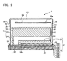
- FIG. 2 is a cross-sectional view of the ink jet head 1 along a shorter direction thereof.
- the ink jet head 1 has a head main body 2, a reservoir unit 71, a COF (Chip On Film) 50, a substrate 54, a side cover 53, and a head cover 55.
- COF Chip On Film
- the reservoir unit 71 is disposed on an upper surface of the head main body 2.
- the reservoir unit 71 is formed from four stacked plates 91 to 94.
- the reservoir unit 71 is formed from an ink inflow passage (not shown), an ink reservoir 61, and ten ink outflow passages 62.
- the ink inflow passage communicates with the ink reservoir 61.
- Each ink outflow passage 62 communicates with the ink reservoir 61. In FIG. 2, only one of the ink outflow passages 62 is shown.
- Ink flows from an ink tank (not shown) into the ink inflow passage.
- the ink reservoir 61 stores the ink temporarily.
- the ink outflow passages 62 communicate with a passage unit 9 via an ink supply opening 105b (see FIG.
- the ink flows from the ink tank to the ink reservoir 61 along the ink inflow passage.
- the ink that has flowed into the ink reservoir 61 passes through the ink outflow passages 62 and is supplied to the passage unit 9 of the head main body 2 via the ink supply opening 105b.
- a concave portion 94a is formed in the plate 94.
- a space is formed between the passage unit 9 and the part of the plate 94 in which the concave portion 94a is formed.
- An actuator unit 21 is disposed within this space.
- One end portion of the COF 50 makes contact with an upper surface of the actuator unit 21.
- Wiring (not shown) is formed at a surface of the COF 50. This wiring is electrically connected with individual electrodes 135 and a common electrode 134 (to be described).
- the COF 50 extends upward from the upper surface of the actuator unit 21.
- the COF 50 passes between the side cover 53 (the right side cover 53 in FIG. 2) and the reservoir unit 71.
- a driver IC 52 is mounted on the COF 50.
- the driver IC 52 is disposed between the side cover 53 and the reservoir unit 71.
- the driver IC 52 generates driving signals for driving the actuator unit 21.
- a sponge 82 is bonded to a side surface of the reservoir unit 71.
- the driver IC 52 is pushed toward the right (toward the side cover 53) by the sponge 82.
- a radiating seat 81 is attached an inner side surface of the side cover 53.
- the driver IC 52 is thermally joined with the side cover 53 by being bonded to the radiating seat 81. Heat from the driver IC 52 is thus radiated to the exterior via the side cover 53.
- the substrate 54 is electrically connected with the COF 50.
- the substrate 54 via the COF 50, commands the driver IC 52 to output driving signals to the actuator unit 21 based on commands from a host controller (not shown).
- the substrate 54 controls the driving of the actuator unit 21.
- the side cover 53 extends upward from both end parts in the widthwise direction of the upper surface of the passage unit 9. Furthermore, a pair of side covers (not shown) also extends upward from both end parts in the lengthwise direction of the upper surface of the passage unit 9 (below, the four side covers will collectively be termed the side cover 53).
- the side cover 53 is a metal plate member.
- the head cover 55 is attached to an upper end of the side cover 53.
- the reservoir unit 71, the COF 50, and the substrate 54 are disposed within a space surrounded by the side cover 53 and the head cover 55.
- a sealing member 56 consisting of silicon resin material, or the like, is spread onto a connecting part of the side cover 53 and the passage unit 9, and onto a fitting part of the side cover 53 and the head cover 55. Ink or ink mist can thus effectively be prevented from entering into the space surrounded by the side cover 53 and the head cover 55 from the exterior.
- FIG. 3 is a plan view of the head main body 2.
- FIG. 4 is an expanded view of a region E1 surrounded by the dashed line shown in FIG. 3.
- pressure chambers 110, apertures 112, and nozzles 108 are shown by solid lines although these are below the actuator unit 21 and should actually be shown by broken lines.
- FIG. 5 shows a cross-sectional view along the line V-V shown in FIG. 4.
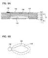
- FIG. 6A is an expanded cross-sectional view of the actuator unit 21.
- FIG. 6B is a plan view of individual electrodes disposed on the surface of the actuator unit 21 in FIG. 6A.
- the head main body 2 contains the passage unit 9, and four actuator units 21.
- the passage unit 9 contains a plurality of the pressure chambers 110, etc.
- the actuator units 21 are fixed to an upper surface 9a of the passage unit 9.
- each actuator unit 21 contains actuators 133 wherein each actuator 133 corresponds to different one pressure chamber 110.
- Each actuator 133 applies discharging energy to the ink within the corresponding pressure chamber 110.
- the passage unit 9 has a rectangular parallelepiped shape that has a plane shape that is substantially the same as the plate 94 of the reservoir unit 71. As shown in FIG. 3, ten ink supply openings 105b open into the upper surface 9a of the passage unit 9. The ink supply openings 105b correspond to the ink outflow passages 62 (see FIG. 2) of the reservoir unit 71. As shown in FIGS. 3 and 4, manifold passages 105 that communicate with the ink supply openings 105b, and sub-manifold passages 105a that bifurcate from the manifold passages 105 are formed within the passage unit 9. As shown in FIGS. 4 and 5, the ink discharge faces 2a are formed in a lower surface of the passage unit 9.
- a plurality of the nozzles 108 is disposed in a matrix state in the ink discharge faces 2a Like the nozzles 108, the pressure chambers 110 are disposed in a matrix state.
- a plurality of pressure chambers 110 aligned equidistantly along the longer direction of the passage unit 9 will be termed a pressure chamber row.
- the pressure chamber rows are mutually parallel in the shorter direction of the passage unit 9.
- the number of pressure chambers 110 included in one pressure chamber row corresponds to the external shape (trapezoid shape) of the actuator units 21 (to be described), and are disposed so as to gradually reduce in number from the longer edge side to the shorter edge side of the trapezoid shape.
- the nozzles 108 are disposed in the same manner.
- the passage unit 9 includes a cavity plate 122, a base plate 123, an aperture plate 124, a supply plate 125, manifold plates 126, 127, 128, a cover plate 129, and a nozzle plate 130.
- These plates 122 to 130 are metal plates formed from stainless steel or the like.
- the plates 122 to 130 have rectangular plan sheet shape that extends in a main scanning direction (the up-down direction in FIG. 3).
- Ten first through holes are formed in the cavity plate 122.
- the first through holes function as ink supply openings 105b (see FIG. 3).
- a plurality of substantially diamond shaped second through holes is formed in the cavity plate 122.
- the second through holes function as the pressure chambers 110.
- Two through holes for each pressure chamber 110 are formed in the base plate 123.
- One of these through holes functions as a communication hole between the pressure chamber 110 and the aperture 112.
- the other of these through holes functions as a communication hole between the pressure chamber 110 and the nozzle 108.
- another ten through holes are also formed in the base plate 123 and function as communication holes between the ink supply openings 105b and the manifold passages 105.
- Through holes are formed in the aperture plate 124 and function as the apertures 112.
- Through holes are formed in the aperture plate 124 and function as communication holes between the pressure chambers 110 and the nozzles 108. Furthermore, ten through holes are formed in the aperture plate 124 and function as communication holes (not shown) between the ink supply openings 105b and the manifold passages 105. Through holes are formed in the supply plate 125 and function as communication holes between the apertures 112 and the sub-manifold passages 105a. Through holes are formed in the supply plate 125 and function as communication holes for the pressure chambers 110 and the nozzles 108. In addition, ten through holes are formed in the supply plate 125 and function as communication holes (not shown) between the ink supply openings 105b and the manifold passages 105.
- a plurality of through holes is formed in the manifold plates 126, 127, 128 and function as communication holes between the pressure chambers 110 and the nozzles 108. Furthermore, through holes are formed in the manifold plates 126, 127, 128 and function as the manifold passages 105 and the sub-manifold passages 105a. Through holes are formed in the cover plate 129 and function as communication holes between the pressure chambers 110 and the nozzles 108. A plurality of through holes is formed in the nozzle plate 130 and function as the nozzles 108. A number of individual ink passages 132 are formed in the passage unit 9 by stacking the plates 122 to 130.
- the ink is fed from the reservoir unit 71 to the interior of the passage unit 9 via the ink supply openings 105b. As shown in FIGS. 3 to 5, the ink that has been fed to the interior of the passage unit 9 flows from the manifold passages 105 into the sub-manifold passages 105a. The ink within the sub-manifold passages 105a reaches the nozzles 108 via the apertures 112 and the pressure chambers 110.
- the actuator units 21 each have a trapezoid shape when viewed in a plan view.
- the four actuator units 21 are disposed in zigzag alignment so as to not interfere with the ink supply openings 105b.
- the long edges and the short edges of the actuator units 21 are parallel to the lengthwise direction of the passage unit 9.
- Two adjoining actuator units 21 overlap in the widthwise direction of the passage unit 9 (in the left-right direction of FIG. 3).
- the actuator unit 21 has three piezoelectric sheets 141 to 143.
- the piezoelectric sheets 141 to 143 are fixed to an upper surface of the cavity plate 122.
- the piezoelectric sheets 141 to 143 are formed from a ferroelectric lead zirconate titanate (PZT) ceramic material.
- the individual electrodes 135 are formed on an upper surface of the uppermost piezoelectric sheet 141.
- the individual electrodes 135 are formed in positions facing the pressure chambers 110.
- the individual electrodes 135 are substantially diamond shaped similar to the pressure chambers 110. In the plan view, the major part of the individual electrodes 135 overlaps with the pressure chambers 110.
- One of the acutely angled sections of the individual electrode 135 extends past the pressure chamber 110.
- a circular land 136 is connected with an anterior tip of the acutely angled section.
- the lands 136 and the individual electrodes 135 are electrically connected.
- the common electrode 134 (ground electrode) is disposed between the piezoelectric sheet 141 and the piezoelectric sheet 142.
- the common electrode 134 is disposed across the entire plane of the piezoelectric sheets 141 and 142.
- One actuator 133 is present for each pressure chamber 110. That is, the actuator units 21 have a plurality of actuators 133.
- Each actuator 133 has one individual electrode 135, the piezoelectric sheets 141, 142, 143, and the common electrode 134.
- Ground potential (reference potential) is applied to the common electrode 134.
- the individual electrodes 135 are electrically connected to a terminal of the driver IC 52 via the lands 136 and internal wiring of the COF 50. Driving signals from the driver IC 52 are selectively input to the individual electrodes 135.
- the piezoelectric sheet 141 is polarized in the direction of thickness by the common electrode 134 and the individual electrodes 135.
- an electric field is applied to the piezoelectric sheet 141 in the direction of polarization (direction of thickness).
- the part of the piezoelectric sheet 141 to which the electric field has been applied functions as an active part that deforms due to piezoelectric effects. For example, if the direction of polarization and the direction in which the electric field is applied are the same, the active part contracts in a direction (the planar direction) orthogonal to the direction of polarization.
- the actuator unit 21 is a unimorph type in which the piezoelectric sheet 141 becomes an active layer that has separated from the pressure chamber 110, and the piezoelectric sheets 142 and 143 close to the pressure chamber 110 are non-active layers. There is a difference between the amount that the active layer (the piezoelectric sheet 141) contracts and the amount that the non-active layers (the piezoelectric sheets 142 and 143) contract. As a result, all of the piezoelectric sheets 141 to 143 collectively deform (unimorph deformation) so as to protrude toward the pressure chamber 110. Pressure (discharging energy) is thus applied to the ink within the pressure chamber 110, and an ink droplet is discharged from the nozzle 108.
- a predetermined potential is applied in advance to the individual electrode 135.
- the driver IC 52 After the individual electrode 135 obtains a ground potential via the driver IC 52 based on a command from the substrate 54, the driver IC 52 outputs a driving signal whereby the aforementioned predetermined potential is applied again at a predetermined timing to the individual electrode 135.
- the piezoelectric sheets 141 to 143 return to their original state with the same timing as when the individual electrode 135 changes from the predetermined potential to the ground potential, and the volume of the pressure chamber 110 is increased with respect to its preliminary state (the state in which voltage was applied in advance).
- the volume of the pressure chamber 110 increases, ink is sucked from the sub-manifold passage 105a into the individual ink passage 132.
- the piezoelectric sheets 141 to 143 deform so as to protrude toward the pressure chamber 110.
- the volume in the pressure chamber 110 thus decreases, the pressure of the ink is increased, and the ink is discharged from the nozzle 108.
- Ink droplets that have adhered to the paper 200 dry rapidly when quick-drying ink is utilized.
- the discharging interval for the ink droplets can consequently be made shorter, and rapid printing becomes possible.
- the ink readily dries within the nozzles 308 and becomes viscous.
- the ink discharge characteristics may deteriorate, and unsatisfactory discharging may occur.
- the ink jet printer 101 selectively performs normal printing in which ink droplets are discharged from the nozzles 108, and non-discharge flushing in which the ink within the nozzles 108 is agitated by causing the vibration of the ink meniscus formed within openings of the nozzles 108.
- the substrate 54 determines, based on the results detected by the paper detecting sensor 59 (see FIG. 7), whether the paper 200 is facing the ink discharge faces 2a.
- the paper detecting sensor 59 detects both edges of the paper 200.
- the timing of the discharge of the ink droplets from the inkjet heads 1 is based on the detection signals of the paper detecting sensor 59. That is, the printing is performed while the paper 200 is facing the ink discharge faces 2a of the inkjet heads 1. Furthermore, the non-discharge flushing is performed while the paper 200 is not facing the ink discharge faces 2a.
- FIG. 7 shows a partial outline view of the internal configuration of the driver IC 52.
- FIG. 7 schematically shows only a configuration (termed driving configuration below) for outputting driving signals to one individual electrode 135 that corresponds to one nozzle 108.
- the driver IC 52 has a plurality of driving configurations that is identical in number to the number of individual electrodes contained in one actuator unit 21.
- the driver IC 52 includes a selector 57a, a pulse outputting part 57b, and a pulse adjusting circuit 58. Based on commands from the substrate 54, the selector 57a selects either a discharge waveform or a non-discharge flushing waveform.
- the discharge waveform is a voltage pulse (a first voltage pulse) for driving the actuator unit 21 such that an ink droplet is discharged from the nozzle 108.
- the non-discharge flushing waveform is a voltage pulse (a second voltage pulse) for driving the actuator unit 21 such that an ink droplet is not discharged from the nozzle 108.
- the selector 57a selects one of the different types of discharge waveforms, and in the case where the command to perform non-discharge flushing has come from the substrate 54, the selector 57a selects the non-discharge flushing waveform.
- the pulse outputting part 57b generates a driving signal that has the waveform selected by the selector 57a, and outputs this driving signal to the individual electrode 135.
- the driving signal output from the pulse outputting part 57b is output to the individual electrode 135 via a resistor R1.
- the resistor R1 determines a current value of the driving signal.
- the pulse adjusting circuit 58 includes a resistor R2 and a switch 58a. Based on commands from the substrate 54, the pulse adjusting circuit 58 adjusts the length of the leading time and the trailing time included in the driving signals output from the pulse outputting part 57b. In a case where the switch 58a is closed, the resistor R1 is connected in parallel with the resistor R2. Specifically, in the case where there was a command from the substrate 54 to perform normal printing, the pulse adjusting circuit 58 opens (turns OFF) the switch 58a. At this juncture, a driving signal having the discharge waveform is applied from the pulse outputting part 57b to the individual electrode 135 via only the resistor R1.
- the pulse adjusting circuit 58 closes (turns ON) the switch 58a.
- a driving signal having the non-discharge flushing waveform is applied from the pulse outputting part 57b to the individual electrode 135 via the resistor R1 and the resistor R2 that are connected in parallel. That is, in a case where the driving signal with the non-discharge flushing waveform is output (in the case where the switch 58a is closed), the resistance between the individual electrode 135 and an output terminal of the pulse outputting part 57b is smaller than the resistance when a driving signal with the discharge waveform is output (in the case where the switch 58a is open). It is possible in the present embodiment, by opening and closing the switch 58a, to switch between a first circuit that includes only the resistor R1, and a second circuit in which the resistor R1 and the resistor R2 are connected in parallel.
- FIG. 8 shows the waveforms of the driving signals output from the driver IC 52.
- FIG. 8A shows an example of a discharge waveform.
- FIG. 8B shows an example of a non-discharge flushing waveform.
- the number of pulses, which are continuous, in the discharge waveform is the same as the number of ink droplets to be discharged (for example, 1 to 3 droplets in the present embodiment).
- a predetermined number of pulses are continuous in the non-discharge flushing waveform.
- a pulse width in the non-discharge flushing waveform is shorter than a pulse width in the discharge waveform.
- the period T1 of the non-discharge flushing waveform is shorter than the period T0 of the discharge waveform.
- the pulse width in the non-discharge flushing waveform is determined to be in a range in which an ink droplet is not discharged from the nozzle 108.
- the pressure reducing period of the non-discharge flushing is set at a value less than or equal to 2/3 of AL.
- the pressure reducing period of the non-discharged flushing may be set within a range of between (2s - 1/2) X AL and (2s + 2/3) X AL (s is positive integer).
- the pressure reducing period is the period from when the pressure in the pressure chamber is being reduced until when the pressure therein begins increasing.
- the amplitude of the voltage pulse of the discharge waveform is the same as the amplitude of the voltage pulse of the non-discharge flushing waveform.
- the utilization of pulse shape in non-discharge flushing is set forth in detail in US Patent Application Publication NO. 2006-0284908 , the contents of which are hereby incorporated by reference into the present application.
- the length of the leading time and the length of the trailing time of the voltage pulse applied to the individual electrode 135 is determined by a time constant calculated from the resistance and capacitance between the output terminal of the pulse outputting part 57b and the individual electrode 135, and from the capacitance of the actuator unit 21 (determined from the configuration of the common electrode 134, the individual electrode 135, and the piezoelectric sheet 141 held between these two).
- the capacitance between the output terminal of the pulse outputting part 57b and the individual electrode 135, and the capacitance of the actuator unit 21 are fixed.
- the length of the leading time and the length of the trailing time of the voltage pulse are adjusted only by the resistance between the output terminal of the pulse outputting part 57b and the individual electrode 135.
- the length of both the leading time and the trailing time of the voltage pulse decreases when the resistance becomes smaller between the output terminal of the pulse outputting part 57b and the individual electrode 135.
- the amplitude does not change even if the resistance changes.
- the length both of the leading time and the trailing time of the voltage pulse decreases, there is an increase in the absolute value of the amount of voltage change (the voltage change) with respect to the leading time and the trailing time of the voltage pulse applied to the individual electrode 135.
- the greater the voltage change of the voltage pulse the faster the deformation speed of the actuator unit 21.
- the resistance between the output terminal of the pulse outputting part 57b and the individual electrode 135 is set such that the voltage change of the voltage pulse of the discharge waveform is a voltage change that allows the ink droplets to be stably discharged from the nozzle 108. As a result, printing can be performed by means of ink droplets that are discharged stably.
- the resistance between the output terminal of the pulse outputting part 57b and the individual electrode 135 is set so it is smaller than the resistance when the driving signal with the discharge waveform is output.
- the voltage change of the voltage pulse of the non-discharge flushing waveform is greater than the voltage change of the voltage pulse of the discharge waveform. That is, the leading time Trf of the non-discharge flushing waveform is shorter than the leading time Trd of the discharge waveform, and the trailing time Tff of the non-discharge flushing waveform is shorter than the trailing time Tfd of the discharge waveform.
- the expansion and contraction speed of the actuator unit 21 is greater in the case where the driving signal with the non-discharge flushing waveform is output than in the case where the driving signal with the discharge waveform is output.
- the pressure wave generated within the individual ink passage 132 has greater amplitude. The non-discharge flushing of the ink within the individual ink passage 132 can thus be performed effectively.
- the resistance of the resistor R2 is adjusted such that the leading time Trf and the trailing time Tff of the non-discharge flushing waveform is 1/n times the period of the characteristic vibration of the actuator unit 21 (n is a positive integer).
- the actuator is capable of vibrating in synchrony with the leading time and trailing time of the voltage pulse of the non-discharge flushing waveform.
- the vibration amplitude of the actuator can also be increased. Non-discharge flushing can consequently be performed more efficiently.
- the voltage change of the voltage pulse of the non-discharge flushing waveform is made greater than the voltage change of the voltage pulse of the discharge waveform by changing the resistance between the individual electrode 135 and the output terminal of the pulse outputting part 57b.
- the pulse adjusting circuit 58 using a simple configuration that does not utilize a condenser, or the like, between the individual electrode 135 and the output terminal of the pulse outputting part 57b.
- the resistance between the individual electrode 135 and the output terminal of the pulse outputting part 57b is changed by switching the switch 58a. It is not necessary to use a changeable resistor, etc. in order to change the resistance between the individual electrode 135 and the output terminal of the pulse outputting part 57b.
- the driver IC 52 can alter the voltage change of the voltage pulse by altering the configuration of the first circuit and the second circuit. Consequently the driver IC 52 needs to comprise only one pulse outputting part 57b.
- the configuration of the ink jet printer 101 can thus be simplified.
- the non-discharge flushing waveform is set to be within a range wherein an ink droplet is not discharged from the nozzle 108. As a result, it is possible to reliably prevent an ink droplet from being discharged from the nozzle 108 while the non-discharge flushing is being performed.
- the amplitude of the discharge waveform is the same as the amplitude of the non-discharge flushing waveform.
- a step-up circuit or step-down circuit is consequently not necessary, and it is possible to realize a pulse outputting part 57b with a simple configuration.
- the pulse outputting part 57b performs the non-discharge flushing only when the paper 200 being transferred by the transfer belt 8 is not facing the nozzle 108.
- the paper 200 is consequently not stained even if an ink droplet is accidentally discharged from the nozzle 108 during non-discharge flushing.
- the pulse adjusting circuit 58 changes the voltage change of the non-discharge flushing waveform both during the leading time and the trailing time.
- the voltage change of the non-discharge flushing waveform may be changed only during either the leading time or the trailing time.
- the leading time Trf and the trailing time Tff of the non-discharge flushing waveform is configured to be 1/n times the period of the characteristic vibration of the actuator unit 21.
- at least one of the leading time and the trailing time of the non-discharge flushing waveform may be configured to not be 1/n times the period of the characteristic vibration of the actuator unit 21.
- the pulse adjusting circuit 58 is in a configuration in which adjusting the voltage change of the voltage pulse is achieved by changing the resistance between the individual electrode 135 and the output terminal of the pulse outputting part 57b.
- the pulse adjusting circuit is not limited to this configuration.
- a resistor and a coil may be connected in series between the output terminal of the pulse outputting part 57b and the individual electrode 135.
- a switch is disposed between the resistor and the coil.
- the resistor and the coil are connected in series (a first circuit). The discharge waveform is applied to the individual electrode 135 via the resistor and the coil.
- the switch is switched, and only the resistor is utilized (a second circuit).
- the non-discharge flushing waveform is applied to the individual electrode 135 via only the resistor.
- the voltage change of the voltage pulse of the non-discharge flushing waveform can be increased by this means also.
- a resistor may be connected between the output terminal of the pulse outputting part 57b and the individual electrode 135, and a condenser, connected in parallel with the actuator unit 21, may be disposed at a lower side of the resistor. In this case, a switch is disposed between the resistor and the condenser.
- a ground potential is applied at the side of the condenser that opposite to the resistor.
- the pulse outputting part 57b outputs the discharge waveform
- the condenser and the actuator unit 21 are connected in parallel (a first circuit).
- the discharge waveform is applied to the individual electrode 135 and the condenser via the resistor.
- the switch is switched, and only the resistor is utilized (a second circuit). That is, the non-discharge flushing waveform is not applied to the condenser.
- the non-discharge flushing waveform is applied to the individual electrode 135 via only the resistor.
- the voltage change of the voltage pulse of the non-discharge flushing waveform can be increased by this means also.
- the pulse outputting part 57b has a configuration wherein it outputs driving signals in which the pulse width of the non-discharge flushing waveform is shorter than the pulse width of the discharge waveform.
- the pulse width of the non-discharge flushing waveform may be differed as necessary.
- the amplitude of the discharge waveform is the same as the amplitude of the non-discharge flushing waveform.
- the amplitude of the waveforms may mutually differ.
- the pulse outputting part 57b is configured so as to perform the non-discharge flushing only when the paper 200 being transferred by the transfer belt 8 is not facing the nozzle 108.
- the pulse outputting part 57b may be configured so as to perform the non-discharge flushing of a nozzle 108, as it is a process that does not discharge ink droplets, while the paper 200 is facing the ink discharge faces 2a.
- This configuration is effective in cases where roll paper is being utilized.
- the non-discharge flushing is performed based not on a signal from the paper detecting sensor 59, but on an output signal from a detecting means that detects the cut lines of the image data, or a measuring means that measures usage time and printing time.
Landscapes
- Particle Formation And Scattering Control In Inkjet Printers (AREA)
- Ink Jet (AREA)
- Luminescent Compositions (AREA)
Abstract
Description
- The present invention relates to an ink jet printer that performs printing by discharging ink droplets.
- An ink jet printer is provided with an ink jet head. A normal ink jet head has a passage unit and an actuator. The passage unit comprises a nozzle, a pressure chamber, and an ink passage located between the nozzle and the pressure chamber. The nozzle discharges ink droplets. The actuator applies pressure (discharging energy) to the ink within the pressure chamber by changing the volume of the pressure chamber. A normal actuator comprises a first electrode, a second electrode to which a reference potential is to be applied, and a piezoelectric element located between the first electrode and the second electrode. The actuator faces the pressure chamber. When a pulsating driving voltage is applied to the first electrode, an electrical field operates in the direction of the thickness on the piezoelectric element. The piezoelectric element that is being acted upon by the electrical field expands or contracts. The volume of the pressure chamber thus changes, and pressure (discharging energy) is applied to the ink within the pressure chamber.
- Ink discharging characteristics may deteriorate when ink within the nozzle becomes more viscous, and unsatisfactory discharging may occur. In order to avoid this problem, discharge flushing may be performed to discharge the viscous ink from the nozzle.
- Ink is consumed when this discharge flushing is performed. In order to avoid this ink consumption, the present inventors considered adopting a technique termed non-discharge flushing wherein an increase in the viscosity of the ink within the nozzle is prevented without ink being consumed. In non-discharge flushing, the actuator is driven such that ink droplets are not discharged from the nozzle, and a pressure wave is generated in the ink within the pressure chamber and the nozzle. The ink is agitated. It is thus possible to prevent the viscosity of the ink from increasing.
- The present inventors discovered that the efficiency of non-discharge flushing is improved by increasing the amplitude of the ink pressure wave. The amplitude of the ink pressure wave increases when the energy applied to the ink within the nozzle is increased. The present inventors discovered that it is possible to increase the energy applied to the ink within the nozzle by increasing the expanding and contracting velocity of the piezoelectric element of the actuator and increasing the vibration of the actuator. The expansion and contraction velocity of the piezoelectric element can be increased by increasing the amount of voltage change during a leading edge period (or a trailing edge period) of a voltage pulse applied to a first electrode (the amount of voltage change is a value wherein the amount of voltage change is divided by the period concerned, and will be termed voltage change' below). However, if the voltage change of the voltage pulse is also increased in the case where printing is to be performed by discharging ink from the nozzle, the ink droplet is not stably discharged from the nozzle. There is a range of voltage change suitable for discharging the ink droplet stably from the nozzle. Consequently, it is preferred that there is not an increase in the voltage change that is applied when printing is to be performed. To deal with this, the present inventors developed a novel technique whereby non-discharge flushing can be performed effectively without having an adverse effect on printing.
- An ink jet printer taught in the present specification includes a passage unit, an actuator and a pulse applying device. The passage unit includes a nozzle, a pressure chamber, and an ink passage located between the nozzle and the pressure chamber. The actuator faces the pressure chamber. The actuator includes a first electrode, a second electrode to which a reference potential is to be applied, and a piezoelectric element located between the first electrode and the second electrode. The pulse applying device is capable of applying a first voltage pulse and a second voltage pulse to the first electrode. The first voltage pulse is applied such that the nozzle discharges an ink droplet The second voltage pulse is applied such that the nozzle does not discharge the ink droplet. A voltage change on a leading edge and/or a trailing edge of the second voltage pulse is greater than a voltage change on a leading edge and/or a trailing edge of the first voltage pulse.
- The aforementioned 'voltage change on a leading edge and/or a trailing edge of the second voltage pulse that is greater than a voltage change on a leading edge and/or a trailing edge of the first voltage pulse' refers to any of the three patterns below:
- (1) The voltage change on the leading edge of the second voltage pulse is greater than the voltage change on the leading edge of the first voltage pulse;
- (2) The voltage change on the trailing edge of the second voltage pulse is greater than the voltage change on the trailing edge of the first voltage pulse; and
- (3) The voltage change on the leading edge of the second voltage pulse is greater than the voltage change on the leading edge of the first voltage pulse, with the voltage change on the trailing edge of the second voltage pulse also being greater than the voltage change on the trailing edge of the first voltage pulse.
- With this ink jet printer, it is possible to adopt the first voltage pulse that maintains a voltage change that allows the ink droplet to be discharged stably. That is, the voltage change of the first voltage pulse is set to be a value in which the ink droplet can be discharged stably. Printing can consequently be performed by ink droplets that are discharged stably. The voltage change of the second voltage pulse is greater than the voltage change of the first voltage pulse. As a result, when non-discharge flushing is performed by means of the second voltage pulse, the expansion and contraction velocity of the piezoelectric element of the actuator can be made greater than the velocity used for printing. In this ink jet printer, it is possible to increase the energy applied by the actuator to the ink within the nozzle during non-discharge flushing. Non-discharge flushing can consequently be performed efficiently.
Furthermore, the aforementioned ink jet printer may perform only non-discharge flushing without performing the discharge flushing. However, the aforementioned technique does not exclude a device which is capable of performing both the discharge flushing and the non-discharge flushing. - In this ink jet printer, the pulse applying device may be capable of applying the second voltage pulse such that the leading time and/or a trailing time of the second voltage pulse is 1/n times the period of the characteristic vibration of the actuator, with n being equal to a positive integer. With this ink jet printer, the actuator is capable of vibrating in synchrony with the leading and/or trailing of the voltage pulse. The amplitude of vibration of the actuator can consequently be increased further.
- In this ink jet printer, the pulse applying device may include a voltage pulse outputting device, a first circuit located between the voltage pulse outputting device and the first electrode, and a second circuit located between the voltage pulse outputting device and the first electrode. In a case where the pulse applying device applies the first voltage pulse to the first electrode, a voltage pulse output by the voltage pulse outputting device may be applied to the first electrode via the first circuit. Furthermore, in a case where the pulse applying device applies the second voltage pulse to the first electrode, the voltage pulse output by the voltage pulse outputting device may be applied to the first electrode via the second circuit. In the case of this ink jet printer, the pulse applying device can alter the voltage change of the voltage pulse by altering the configuration of the first circuit and the second circuit. Consequently the pulse applying device needs to comprise only one voltage outputting device. The configuration of the ink jet printer can thus be simplified.
- Furthermore, with the pulse applying device, a resistance of the first circuit may be greater than a resistance of the second circuit. With this configuration, the voltage change of the voltage pulse can be changed by changing the resistance to the first electrode from the pulse outputting device. As a result, the first circuit and the second circuit can be configured using only resistors. The configuration of the ink jet printer can thus be simplified. Furthermore, the first circuit may include a first resistor, and the second circuit may include the first resistor and a second resistor connected in parallel with the first resistor. With this configuration, it is not necessary to use a changeable resistor, etc. in order to change the resistance to the first electrode from the pulse outputting device.
- In this ink jet printer, an amplitude of the first voltage pulse may be the same as an amplitude of the second voltage pulse.
- Furthermore, the ink jet printer may include a transferring device and a detecting device. The transferring device may transfer a print medium. The detecting device may detect that the print medium transferred by the transferring device is facing the nozzle. In this case the pulse applying device may apply the second voltage pulse when the print medium is not facing the nozzle. The medium to be printed is consequently not stained even if an ink droplet has been discharged accidentally from the nozzle.
-
- FIG. 1 shows an outline side view of the entire configuration of an ink jet printer.
- FIG. 2 shows a cross-sectional view of the ink jet head along a shorter direction thereof.
- FIG. 3 shows a plan view of a head main body.
- FIG. 4 shows an expanded view of a region E1 shown in FIG. 3.
- FIG. 5 shows a cross-sectional view along the line V-V shown in FIG. 4.
- FIG. 6 shows expanded views of an actuator unit.
- FIG. 7 shows a partial outline view of the internal configuration of a driver IC.
- FIG. 8 shows waveforms output from the driver IC.
- A suitable embodiment of the present invention will be described below with reference to the figures. FIG. 1 shows an outline side view of the entire configuration of an ink jet printer 101 (hereafter referred to as printer 101). As shown in F1G. 1, the
printer 101 is a color ink jet printer that has four ink jet heads 1. In this printer 101 apaper feeding part 11 is on the left, and apaper discharge part 12 is on the right - A paper transferring path for transferring paper (a print medium) 200 from the
paper feeding part 11 toward thepaper discharge part 12 is formed within theprinter 101. A pair oftransfer rollers paper feeding part 11. The pair oftransfer rollers paper 200 from thepaper feeding part 11 toward the right. A belt transferring mechanism (paper transferring mechanism) 13 is disposed in a central portion of the paper transferring path. Thebelt transferring mechanism 13 has two belt rollers 6 and 7, atransfer belt 8, and aplaten 15. Thetransfer belt 8 is wound around the belt rollers 6 and 7. Thetransfer belt 8 is adjusted to have a length such that a predetermined tension is generated when it is wound around the belt rollers 6 and 7. Theplaten 15 is disposed within a region surrounded by thetransfer belt 8. Theplaten 15 is disposed in a position facing theink jet head 1. Theplaten 15 supports thetransfer belt 8 so that thetransfer belt 8 does not bend downward. Anip roller 4 is disposed in a position facing the belt roller 7. Thenip roller 4 presses thepaper 200 against an outerperipheral surface 8a of thetransfer belt 8. - The belt roller 6 is rotated by a transfer motor (not shown). The
transfer belt 8 is driven by the rotation of the belt roller 6. Thetransfer belt 8 thus supports thepaper 200, and transfers it toward thepaper discharge part 12. - A
separating mechanism 14 is disposed at a downstream side, in the direction of paper transferring, of thetransfer belt 8. Theseparating mechanism 14 separates thepaper 200 from the outerperipheral plane 8a of thetransfer belt 8. Thepaper 200 that has been separated from thetransfer belt 8 by theseparating mechanism 14 is delivered toward thepaper discharge part 12. - The four ink jet heads 1 correspond to four colors of ink (magenta, yellow, cyan, and black). The four ink jet heads 1 are aligned along the transferring direction. That is, the
ink jet printer 101 is a line type printer. A lower end of each of the ink jet heads 1 has a headmain body 2. The headmain bodies 2 are aligned in a rectangular parallelepiped shape that extends in a direction orthogonal to the transferring direction (perpendicular relative to the plane of the page of FIG. 1). Anink discharge face 2a is formed at a bottom face of each headmain body 2. The ink discharge faces 2a face the outerperipheral plane 8a. Thepaper 200 passes in sequence below the four headmain bodies 2. At this juncture, the ink is discharged from the ink discharge faces 2a toward an upper surface of thepaper 200. Theprinter 101 thus forms a desired color image on the upper surface of thepaper 200.
Furthermore, theprinter 101 also comprises apaper detecting sensor 59. Thepaper detecting sensor 59 is disposed downstream from thenip roller 4. Thepaper detecting sensor 59 is capable of detecting whether paper is present. - Next, the
ink jet head 1 will be described in detail with reference to FIG. 2. FIG. 2 is a cross-sectional view of theink jet head 1 along a shorter direction thereof. As shown in FIG. 2, theink jet head 1 has a headmain body 2, a reservoir unit 71, a COF (Chip On Film) 50, asubstrate 54, aside cover 53, and ahead cover 55. - The reservoir unit 71 is disposed on an upper surface of the head
main body 2. The reservoir unit 71 is formed from four stackedplates 91 to 94. The reservoir unit 71 is formed from an ink inflow passage (not shown), anink reservoir 61, and tenink outflow passages 62. The ink inflow passage communicates with theink reservoir 61. Eachink outflow passage 62 communicates with theink reservoir 61. In FIG. 2, only one of theink outflow passages 62 is shown. Ink flows from an ink tank (not shown) into the ink inflow passage. Theink reservoir 61 stores the ink temporarily. Theink outflow passages 62 communicate with apassage unit 9 via anink supply opening 105b (see FIG. 3) formed in an upper surface of thepassage unit 9. The ink flows from the ink tank to theink reservoir 61 along the ink inflow passage. The ink that has flowed into theink reservoir 61 passes through theink outflow passages 62 and is supplied to thepassage unit 9 of the headmain body 2 via theink supply opening 105b. Aconcave portion 94a is formed in theplate 94. A space is formed between thepassage unit 9 and the part of theplate 94 in which theconcave portion 94a is formed. Anactuator unit 21 is disposed within this space. - One end portion of the
COF 50 makes contact with an upper surface of theactuator unit 21. Wiring (not shown) is formed at a surface of theCOF 50. This wiring is electrically connected withindividual electrodes 135 and a common electrode 134 (to be described). TheCOF 50 extends upward from the upper surface of theactuator unit 21. TheCOF 50 passes between the side cover 53 (theright side cover 53 in FIG. 2) and the reservoir unit 71. Adriver IC 52 is mounted on theCOF 50. Thedriver IC 52 is disposed between theside cover 53 and the reservoir unit 71. Thedriver IC 52 generates driving signals for driving theactuator unit 21. Asponge 82 is bonded to a side surface of the reservoir unit 71. Thedriver IC 52 is pushed toward the right (toward the side cover 53) by thesponge 82. A radiatingseat 81 is attached an inner side surface of theside cover 53. Thedriver IC 52 is thermally joined with theside cover 53 by being bonded to the radiatingseat 81. Heat from thedriver IC 52 is thus radiated to the exterior via theside cover 53. - The
substrate 54 is electrically connected with theCOF 50. Thesubstrate 54, via theCOF 50, commands thedriver IC 52 to output driving signals to theactuator unit 21 based on commands from a host controller (not shown). Thesubstrate 54 controls the driving of theactuator unit 21. - The side cover 53 extends upward from both end parts in the widthwise direction of the upper surface of the
passage unit 9. Furthermore, a pair of side covers (not shown) also extends upward from both end parts in the lengthwise direction of the upper surface of the passage unit 9 (below, the four side covers will collectively be termed the side cover 53). The side cover 53 is a metal plate member. Thehead cover 55 is attached to an upper end of theside cover 53. The reservoir unit 71, theCOF 50, and thesubstrate 54 are disposed within a space surrounded by theside cover 53 and thehead cover 55. A sealingmember 56 consisting of silicon resin material, or the like, is spread onto a connecting part of theside cover 53 and thepassage unit 9, and onto a fitting part of theside cover 53 and thehead cover 55. Ink or ink mist can thus effectively be prevented from entering into the space surrounded by theside cover 53 and the head cover 55 from the exterior. - Next, the head
main body 2 will be described with reference to FIGS. 3 to 6. FIG. 3 is a plan view of the headmain body 2. FIG. 4 is an expanded view of a region E1 surrounded by the dashed line shown in FIG. 3. In FIG. 4,pressure chambers 110,apertures 112, andnozzles 108 are shown by solid lines although these are below theactuator unit 21 and should actually be shown by broken lines. FIG. 5 shows a cross-sectional view along the line V-V shown in FIG. 4. FIG. 6A is an expanded cross-sectional view of theactuator unit 21. FIG. 6B is a plan view of individual electrodes disposed on the surface of theactuator unit 21 in FIG. 6A. - As shown in FIG. 3, the head
main body 2 contains thepassage unit 9, and fouractuator units 21. As shown in FIG. 4, thepassage unit 9 contains a plurality of thepressure chambers 110, etc. Theactuator units 21 are fixed to anupper surface 9a of thepassage unit 9. As shown in FIG. 6A, eachactuator unit 21 containsactuators 133 wherein each actuator 133 corresponds to different onepressure chamber 110. Eachactuator 133 applies discharging energy to the ink within the correspondingpressure chamber 110. - The
passage unit 9 has a rectangular parallelepiped shape that has a plane shape that is substantially the same as theplate 94 of the reservoir unit 71. As shown in FIG. 3, tenink supply openings 105b open into theupper surface 9a of thepassage unit 9. Theink supply openings 105b correspond to the ink outflow passages 62 (see FIG. 2) of the reservoir unit 71. As shown in FIGS. 3 and 4,manifold passages 105 that communicate with theink supply openings 105b, andsub-manifold passages 105a that bifurcate from themanifold passages 105 are formed within thepassage unit 9. As shown in FIGS. 4 and 5, the ink discharge faces 2a are formed in a lower surface of thepassage unit 9. A plurality of thenozzles 108 is disposed in a matrix state in the ink discharge faces 2a Like thenozzles 108, thepressure chambers 110 are disposed in a matrix state. Below, a plurality ofpressure chambers 110 aligned equidistantly along the longer direction of thepassage unit 9 will be termed a pressure chamber row. There are sixteen pressure chamber rows. The pressure chamber rows are mutually parallel in the shorter direction of thepassage unit 9. The number ofpressure chambers 110 included in one pressure chamber row corresponds to the external shape (trapezoid shape) of the actuator units 21 (to be described), and are disposed so as to gradually reduce in number from the longer edge side to the shorter edge side of the trapezoid shape. Thenozzles 108 are disposed in the same manner. - As shown in FIG. 5, the
passage unit 9 includes acavity plate 122, abase plate 123, anaperture plate 124, asupply plate 125,manifold plates cover plate 129, and anozzle plate 130. Theseplates 122 to 130 are metal plates formed from stainless steel or the like. Theplates 122 to 130 have rectangular plan sheet shape that extends in a main scanning direction (the up-down direction in FIG. 3). - Ten first through holes are formed in the
cavity plate 122. The first through holes function asink supply openings 105b (see FIG. 3). Furthermore, a plurality of substantially diamond shaped second through holes is formed in thecavity plate 122. The second through holes function as thepressure chambers 110. Two through holes for eachpressure chamber 110 are formed in thebase plate 123. One of these through holes functions as a communication hole between thepressure chamber 110 and theaperture 112. The other of these through holes functions as a communication hole between thepressure chamber 110 and thenozzle 108. Furthermore, another ten through holes are also formed in thebase plate 123 and function as communication holes between theink supply openings 105b and themanifold passages 105. Through holes are formed in theaperture plate 124 and function as theapertures 112. Through holes are formed in theaperture plate 124 and function as communication holes between thepressure chambers 110 and thenozzles 108. Furthermore, ten through holes are formed in theaperture plate 124 and function as communication holes (not shown) between theink supply openings 105b and themanifold passages 105. Through holes are formed in thesupply plate 125 and function as communication holes between theapertures 112 and thesub-manifold passages 105a. Through holes are formed in thesupply plate 125 and function as communication holes for thepressure chambers 110 and thenozzles 108. In addition, ten through holes are formed in thesupply plate 125 and function as communication holes (not shown) between theink supply openings 105b and themanifold passages 105. - A plurality of through holes is formed in the
manifold plates pressure chambers 110 and thenozzles 108. Furthermore, through holes are formed in themanifold plates manifold passages 105 and thesub-manifold passages 105a. Through holes are formed in thecover plate 129 and function as communication holes between thepressure chambers 110 and thenozzles 108. A plurality of through holes is formed in thenozzle plate 130 and function as thenozzles 108. A number ofindividual ink passages 132 are formed in thepassage unit 9 by stacking theplates 122 to 130. - Next, the flow of ink within the
passage unit 9 will be described. The ink is fed from the reservoir unit 71 to the interior of thepassage unit 9 via theink supply openings 105b. As shown in FIGS. 3 to 5, the ink that has been fed to the interior of thepassage unit 9 flows from themanifold passages 105 into thesub-manifold passages 105a. The ink within thesub-manifold passages 105a reaches thenozzles 108 via theapertures 112 and thepressure chambers 110. - The
actuator units 21 will now be described. As shown in FIG. 3, theactuator units 21 each have a trapezoid shape when viewed in a plan view. The fouractuator units 21 are disposed in zigzag alignment so as to not interfere with theink supply openings 105b. The long edges and the short edges of theactuator units 21 are parallel to the lengthwise direction of thepassage unit 9. Two adjoiningactuator units 21 overlap in the widthwise direction of the passage unit 9 (in the left-right direction of FIG. 3). - As shown in FIG. 6A, the
actuator unit 21 has threepiezoelectric sheets 141 to 143. Thepiezoelectric sheets 141 to 143 are fixed to an upper surface of thecavity plate 122. Thepiezoelectric sheets 141 to 143 are formed from a ferroelectric lead zirconate titanate (PZT) ceramic material. Theindividual electrodes 135 are formed on an upper surface of the uppermostpiezoelectric sheet 141. Theindividual electrodes 135 are formed in positions facing thepressure chambers 110. As shown in FIG. 6B, theindividual electrodes 135 are substantially diamond shaped similar to thepressure chambers 110. In the plan view, the major part of theindividual electrodes 135 overlaps with thepressure chambers 110. One of the acutely angled sections of theindividual electrode 135 extends past thepressure chamber 110. Acircular land 136 is connected with an anterior tip of the acutely angled section. Thelands 136 and theindividual electrodes 135 are electrically connected. The common electrode 134 (ground electrode) is disposed between thepiezoelectric sheet 141 and thepiezoelectric sheet 142. Thecommon electrode 134 is disposed across the entire plane of thepiezoelectric sheets actuator 133 is present for eachpressure chamber 110. That is, theactuator units 21 have a plurality ofactuators 133. Eachactuator 133 has oneindividual electrode 135, thepiezoelectric sheets common electrode 134. - Ground potential (reference potential) is applied to the
common electrode 134. Theindividual electrodes 135 are electrically connected to a terminal of thedriver IC 52 via thelands 136 and internal wiring of theCOF 50. Driving signals from thedriver IC 52 are selectively input to theindividual electrodes 135. - The
piezoelectric sheet 141 is polarized in the direction of thickness by thecommon electrode 134 and theindividual electrodes 135. When voltage is applied to theindividual electrode 135 and theindividual electrode 135 has a different potential from thecommon electrode 134, an electric field is applied to thepiezoelectric sheet 141 in the direction of polarization (direction of thickness). The part of thepiezoelectric sheet 141 to which the electric field has been applied functions as an active part that deforms due to piezoelectric effects. For example, if the direction of polarization and the direction in which the electric field is applied are the same, the active part contracts in a direction (the planar direction) orthogonal to the direction of polarization. That is, theactuator unit 21 is a unimorph type in which thepiezoelectric sheet 141 becomes an active layer that has separated from thepressure chamber 110, and thepiezoelectric sheets pressure chamber 110 are non-active layers. There is a difference between the amount that the active layer (the piezoelectric sheet 141) contracts and the amount that the non-active layers (thepiezoelectric sheets 142 and 143) contract. As a result, all of thepiezoelectric sheets 141 to 143 collectively deform (unimorph deformation) so as to protrude toward thepressure chamber 110. Pressure (discharging energy) is thus applied to the ink within thepressure chamber 110, and an ink droplet is discharged from thenozzle 108. - In the present embodiment, a predetermined potential is applied in advance to the
individual electrode 135. After theindividual electrode 135 obtains a ground potential via thedriver IC 52 based on a command from thesubstrate 54, thedriver IC 52 outputs a driving signal whereby the aforementioned predetermined potential is applied again at a predetermined timing to theindividual electrode 135. In this case, thepiezoelectric sheets 141 to 143 return to their original state with the same timing as when theindividual electrode 135 changes from the predetermined potential to the ground potential, and the volume of thepressure chamber 110 is increased with respect to its preliminary state (the state in which voltage was applied in advance). When the volume of thepressure chamber 110 increases, ink is sucked from thesub-manifold passage 105a into theindividual ink passage 132. Then when the predetermined potential is again applied to theindividual electrode 135, thepiezoelectric sheets 141 to 143 deform so as to protrude toward thepressure chamber 110. The volume in thepressure chamber 110 thus decreases, the pressure of the ink is increased, and the ink is discharged from thenozzle 108. - Ink droplets that have adhered to the
paper 200 dry rapidly when quick-drying ink is utilized. The discharging interval for the ink droplets can consequently be made shorter, and rapid printing becomes possible. However, when quick-drying ink is utilized, the ink readily dries within the nozzles 308 and becomes viscous. When the ink within thenozzles 108 is viscous, the ink discharge characteristics may deteriorate, and unsatisfactory discharging may occur. To deal with this, theink jet printer 101 selectively performs normal printing in which ink droplets are discharged from thenozzles 108, and non-discharge flushing in which the ink within thenozzles 108 is agitated by causing the vibration of the ink meniscus formed within openings of thenozzles 108. - Specifically, the
substrate 54 determines, based on the results detected by the paper detecting sensor 59 (see FIG. 7), whether thepaper 200 is facing the ink discharge faces 2a. Thepaper detecting sensor 59 detects both edges of thepaper 200. The timing of the discharge of the ink droplets from the inkjet heads 1 is based on the detection signals of thepaper detecting sensor 59. That is, the printing is performed while thepaper 200 is facing the ink discharge faces 2a of the inkjet heads 1. Furthermore, the non-discharge flushing is performed while thepaper 200 is not facing the ink discharge faces 2a. - Next, the
driver IC 52 will be described in detail with reference to FIG. 7. FIG. 7 shows a partial outline view of the internal configuration of thedriver IC 52. FIG. 7 schematically shows only a configuration (termed driving configuration below) for outputting driving signals to oneindividual electrode 135 that corresponds to onenozzle 108. Thedriver IC 52 has a plurality of driving configurations that is identical in number to the number of individual electrodes contained in oneactuator unit 21. Thedriver IC 52 includes aselector 57a, apulse outputting part 57b, and apulse adjusting circuit 58. Based on commands from thesubstrate 54, theselector 57a selects either a discharge waveform or a non-discharge flushing waveform. The discharge waveform is a voltage pulse (a first voltage pulse) for driving theactuator unit 21 such that an ink droplet is discharged from thenozzle 108. There are a number of discharge waveform patterns that correspond to the various types of ink droplets to be discharged from thenozzle 108. The non-discharge flushing waveform is a voltage pulse (a second voltage pulse) for driving theactuator unit 21 such that an ink droplet is not discharged from thenozzle 108. In the case where the command to perform printing has come from thesubstrate 54, theselector 57a selects one of the different types of discharge waveforms, and in the case where the command to perform non-discharge flushing has come from thesubstrate 54, theselector 57a selects the non-discharge flushing waveform. Thepulse outputting part 57b generates a driving signal that has the waveform selected by theselector 57a, and outputs this driving signal to theindividual electrode 135. The driving signal output from thepulse outputting part 57b is output to theindividual electrode 135 via a resistor R1. The resistor R1 determines a current value of the driving signal. - The
pulse adjusting circuit 58 includes a resistor R2 and aswitch 58a. Based on commands from thesubstrate 54, thepulse adjusting circuit 58 adjusts the length of the leading time and the trailing time included in the driving signals output from thepulse outputting part 57b. In a case where theswitch 58a is closed, the resistor R1 is connected in parallel with the resistor R2. Specifically, in the case where there was a command from thesubstrate 54 to perform normal printing, thepulse adjusting circuit 58 opens (turns OFF) theswitch 58a. At this juncture, a driving signal having the discharge waveform is applied from thepulse outputting part 57b to theindividual electrode 135 via only the resistor R1. In the case where there was a command from thesubstrate 54 to perform non-discharge flushing, thepulse adjusting circuit 58 closes (turns ON) theswitch 58a. In this case, a driving signal having the non-discharge flushing waveform is applied from thepulse outputting part 57b to theindividual electrode 135 via the resistor R1 and the resistor R2 that are connected in parallel. That is, in a case where the driving signal with the non-discharge flushing waveform is output (in the case where theswitch 58a is closed), the resistance between theindividual electrode 135 and an output terminal of thepulse outputting part 57b is smaller than the resistance when a driving signal with the discharge waveform is output (in the case where theswitch 58a is open). It is possible in the present embodiment, by opening and closing theswitch 58a, to switch between a first circuit that includes only the resistor R1, and a second circuit in which the resistor R1 and the resistor R2 are connected in parallel. - Waveforms of the driving signals output from the
driver IC 52 will be described with reference to FIG. 8. FIG. 8 shows the waveforms of the driving signals output from thedriver IC 52. FIG. 8A shows an example of a discharge waveform. FIG. 8B shows an example of a non-discharge flushing waveform. As shown in FIG. 8A, the number of pulses, which are continuous, in the discharge waveform is the same as the number of ink droplets to be discharged (for example, 1 to 3 droplets in the present embodiment). As shown in FIG. 8B, a predetermined number of pulses are continuous in the non-discharge flushing waveform. A pulse width in the non-discharge flushing waveform is shorter than a pulse width in the discharge waveform. The period T1 of the non-discharge flushing waveform is shorter than the period T0 of the discharge waveform. The pulse width in the non-discharge flushing waveform is determined to be in a range in which an ink droplet is not discharged from thenozzle 108. Specifically, in a case where the a pressure reducing period (period from a trailing to a leading of one pulse) is AL in order to realize the maximum discharging speed of the ink discharged from the nozzle, the pressure reducing period of the non-discharge flushing is set at a value less than or equal to 2/3 of AL. In addition, the pressure reducing period of the non-discharged flushing may be set within a range of between (2s - 1/2) X AL and (2s + 2/3) X AL (s is positive integer). The pressure reducing period is the period from when the pressure in the pressure chamber is being reduced until when the pressure therein begins increasing. Furthermore, the amplitude of the voltage pulse of the discharge waveform is the same as the amplitude of the voltage pulse of the non-discharge flushing waveform. Additionally, the utilization of pulse shape in non-discharge flushing is set forth in detail inUS Patent Application Publication NO. 2006-0284908 , the contents of which are hereby incorporated by reference into the present application. - The length of the leading time and the length of the trailing time of the voltage pulse applied to the
individual electrode 135 is determined by a time constant calculated from the resistance and capacitance between the output terminal of thepulse outputting part 57b and theindividual electrode 135, and from the capacitance of the actuator unit 21 (determined from the configuration of thecommon electrode 134, theindividual electrode 135, and thepiezoelectric sheet 141 held between these two). In the present embodiment, the capacitance between the output terminal of thepulse outputting part 57b and theindividual electrode 135, and the capacitance of theactuator unit 21 are fixed. As a result, the length of the leading time and the length of the trailing time of the voltage pulse are adjusted only by the resistance between the output terminal of thepulse outputting part 57b and theindividual electrode 135. That is, the length of both the leading time and the trailing time of the voltage pulse decreases when the resistance becomes smaller between the output terminal of thepulse outputting part 57b and theindividual electrode 135. The amplitude does not change even if the resistance changes. As a result, when the length both of the leading time and the trailing time of the voltage pulse decreases, there is an increase in the absolute value of the amount of voltage change (the voltage change) with respect to the leading time and the trailing time of the voltage pulse applied to theindividual electrode 135. The greater the voltage change of the voltage pulse, the faster the deformation speed of theactuator unit 21. - As described above, in the case where the driving signal with the discharge waveform is output, the resistance between the output terminal of the
pulse outputting part 57b and theindividual electrode 135 is set such that the voltage change of the voltage pulse of the discharge waveform is a voltage change that allows the ink droplets to be stably discharged from thenozzle 108. As a result, printing can be performed by means of ink droplets that are discharged stably. In the case where the driving signal with the non-discharge flushing waveform is output, the resistance between the output terminal of thepulse outputting part 57b and theindividual electrode 135 is set so it is smaller than the resistance when the driving signal with the discharge waveform is output. As a result, the voltage change of the voltage pulse of the non-discharge flushing waveform is greater than the voltage change of the voltage pulse of the discharge waveform. That is, the leading time Trf of the non-discharge flushing waveform is shorter than the leading time Trd of the discharge waveform, and the trailing time Tff of the non-discharge flushing waveform is shorter than the trailing time Tfd of the discharge waveform. The expansion and contraction speed of theactuator unit 21 is greater in the case where the driving signal with the non-discharge flushing waveform is output than in the case where the driving signal with the discharge waveform is output. When the expanding and contracting speed of theactuator unit 21 is greater, the pressure wave generated within theindividual ink passage 132 has greater amplitude. The non-discharge flushing of the ink within theindividual ink passage 132 can thus be performed effectively. - In the present embodiment, the resistance of the resistor R2 is adjusted such that the leading time Trf and the trailing time Tff of the non-discharge flushing waveform is 1/n times the period of the characteristic vibration of the actuator unit 21 (n is a positive integer). The actuator is capable of vibrating in synchrony with the leading time and trailing time of the voltage pulse of the non-discharge flushing waveform. The vibration amplitude of the actuator can also be increased. Non-discharge flushing can consequently be performed more efficiently.
- In the present embodiment, the voltage change of the voltage pulse of the non-discharge flushing waveform is made greater than the voltage change of the voltage pulse of the discharge waveform by changing the resistance between the
individual electrode 135 and the output terminal of thepulse outputting part 57b. As a result, it is possible to realize thepulse adjusting circuit 58 using a simple configuration that does not utilize a condenser, or the like, between theindividual electrode 135 and the output terminal of thepulse outputting part 57b. Furthermore, the resistance between theindividual electrode 135 and the output terminal of thepulse outputting part 57b is changed by switching theswitch 58a. It is not necessary to use a changeable resistor, etc. in order to change the resistance between theindividual electrode 135 and the output terminal of thepulse outputting part 57b. - In the present embodiment, the
driver IC 52 can alter the voltage change of the voltage pulse by altering the configuration of the first circuit and the second circuit. Consequently thedriver IC 52 needs to comprise only onepulse outputting part 57b. The configuration of theink jet printer 101 can thus be simplified. - Furthermore, in the present embodiment, the non-discharge flushing waveform is set to be within a range wherein an ink droplet is not discharged from the
nozzle 108. As a result, it is possible to reliably prevent an ink droplet from being discharged from thenozzle 108 while the non-discharge flushing is being performed. - In addition, in the present embodiment, the amplitude of the discharge waveform is the same as the amplitude of the non-discharge flushing waveform. A step-up circuit or step-down circuit is consequently not necessary, and it is possible to realize a
pulse outputting part 57b with a simple configuration. - Furthermore, in the present embodiment, the
pulse outputting part 57b performs the non-discharge flushing only when thepaper 200 being transferred by thetransfer belt 8 is not facing thenozzle 108. Thepaper 200 is consequently not stained even if an ink droplet is accidentally discharged from thenozzle 108 during non-discharge flushing. - A suitable embodiment of the present invention has been described above, but the present invention is not limited to the specific example described above, and the art set forth in the claims encompasses various transformations and modifications to the embodiment described above. For example, in the embodiment described above, the
pulse adjusting circuit 58 changes the voltage change of the non-discharge flushing waveform both during the leading time and the trailing time. However, the voltage change of the non-discharge flushing waveform may be changed only during either the leading time or the trailing time. - In the embodiment described above, the leading time Trf and the trailing time Tff of the non-discharge flushing waveform is configured to be 1/n times the period of the characteristic vibration of the
actuator unit 21. However, at least one of the leading time and the trailing time of the non-discharge flushing waveform may be configured to not be 1/n times the period of the characteristic vibration of theactuator unit 21. - Furthermore, in the embodiment described above, the
pulse adjusting circuit 58 is in a configuration in which adjusting the voltage change of the voltage pulse is achieved by changing the resistance between theindividual electrode 135 and the output terminal of thepulse outputting part 57b. However, the pulse adjusting circuit is not limited to this configuration. For example, in the pulse adjusting circuit, a resistor and a coil may be connected in series between the output terminal of thepulse outputting part 57b and theindividual electrode 135. In this case, a switch is disposed between the resistor and the coil. In the case where thepulse outputting part 57b outputs the discharge waveform, the resistor and the coil are connected in series (a first circuit). The discharge waveform is applied to theindividual electrode 135 via the resistor and the coil. In the case where thepulse outputting part 57b outputs the non-discharge flushing waveform, the switch is switched, and only the resistor is utilized (a second circuit). The non-discharge flushing waveform is applied to theindividual electrode 135 via only the resistor. The voltage change of the voltage pulse of the non-discharge flushing waveform can be increased by this means also. Furthermore, for example, in the pulse adjusting circuit, a resistor may be connected between the output terminal of thepulse outputting part 57b and theindividual electrode 135, and a condenser, connected in parallel with theactuator unit 21, may be disposed at a lower side of the resistor. In this case, a switch is disposed between the resistor and the condenser. A ground potential (reference potential) is applied at the side of the condenser that opposite to the resistor. In the case where thepulse outputting part 57b outputs the discharge waveform, the condenser and theactuator unit 21 are connected in parallel (a first circuit). The discharge waveform is applied to theindividual electrode 135 and the condenser via the resistor. In the case where thepulse outputting part 57b outputs the non-discharge flushing waveform, the switch is switched, and only the resistor is utilized (a second circuit). That is, the non-discharge flushing waveform is not applied to the condenser. The non-discharge flushing waveform is applied to theindividual electrode 135 via only the resistor. The voltage change of the voltage pulse of the non-discharge flushing waveform can be increased by this means also. - In the embodiment described above, the
pulse outputting part 57b has a configuration wherein it outputs driving signals in which the pulse width of the non-discharge flushing waveform is shorter than the pulse width of the discharge waveform. However, the pulse width of the non-discharge flushing waveform may be differed as necessary. - Furthermore, in the embodiment described above, the amplitude of the discharge waveform is the same as the amplitude of the non-discharge flushing waveform. However, the amplitude of the waveforms may mutually differ.
- Furthermore, in the embodiment described above, the
pulse outputting part 57b is configured so as to perform the non-discharge flushing only when thepaper 200 being transferred by thetransfer belt 8 is not facing thenozzle 108. However, thepulse outputting part 57b may be configured so as to perform the non-discharge flushing of anozzle 108, as it is a process that does not discharge ink droplets, while thepaper 200 is facing the ink discharge faces 2a. This configuration is effective in cases where roll paper is being utilized. In this situation, the non-discharge flushing is performed based not on a signal from thepaper detecting sensor 59, but on an output signal from a detecting means that detects the cut lines of the image data, or a measuring means that measures usage time and printing time.
Claims (7)
- An ink jet printer (101), comprising:a passage unit (9) comprising a nozzle (108), a pressure chamber (110), and an ink passage (132) located between the nozzle (108) and the pressure chamber (110);an actuator (21) facing the pressure chamber (110), the actuator (21) comprising a first electrode (135), a second electrode (134) to which a reference potential can be applied, and a piezoelectric element (141) located between the first electrode (135) and the second electrode (134);a pulse applying device (52) which applies a first voltage pulse to the first electrode (135) such that the nozzle (108) discharges an ink droplet, and a second voltage pulse to the first electrode (135) such that the nozzle (108) does not discharge the ink droplet, wherein a voltage change on a leading edge and/or a trailing edge of the second voltage pulse is greater than a voltage change on a leading edge and/or a trailing edge of the first voltage pulse.
- The inkjet printer (101) as in claim 1, wherein
the pulse applying device (52) applies the second voltage pulse such that a leading time and/or a trailing time of the second voltage pulse is 1/n times a period of a characteristic vibration of the actuator (21), and
n is a positive integer. - The ink jet printer (101) as in claim 1 or 2, wherein
the pulse applying device (52) comprises a voltage pulse outputting device (57b), a first circuit (R1) located between the voltage pulse outputting device (57b) and the first electrode (135), and a second circuit (R1, 58) located between the voltage pulse outputting device (57b) and the first electrode (135),
in a case where the pulse applying device (52) applies the first voltage pulse to the first electrode (135), a voltage pulse output by the voltage pulse outputting device (57b) is applied to the first electrode (135) via the first circuit (R1), and
in a case where the pulse applying device (52) applies the second voltage pulse to the first electrode (135), the voltage pulse output by the voltage pulse outputting device (57b) is applied to the first electrode (135) via the second circuit (R1, 58). - The ink jet printer (101) as in claim 3, wherein
a resistance of the first circuit (R1) is greater than a resistance of the second circuit (R1, 58). - The ink jet printer (101) as in claim 4, wherein
the first circuit comprises a first resistor (R1), and
the second circuit comprises the first resistor (R1) and a second resistor (R2) connected in parallel with the first resistor (R1). - The ink jet printer (101) as in any one of claims 1 to 5, wherein
an amplitude of the first voltage pulse is the same as an amplitude of the second voltage pulse. - The ink jet printer (101) as in any one of claims 1 to 6, further comprising:a transferring device (8) transferring a print medium (200); anda detecting device (59) detecting that the print medium (200) transferred by the transferring device (8) is facing the nozzle (108),wherein the pulse applying device (52) applies the second voltage pulse to the first electrode (135) when the print medium (200) is not facing the nozzle (108).
Applications Claiming Priority (1)
| Application Number | Priority Date | Filing Date | Title |
|---|---|---|---|
| JP2006142293A JP4259544B2 (en) | 2006-05-23 | 2006-05-23 | Inkjet printer |
Publications (2)
| Publication Number | Publication Date |
|---|---|
| EP1859940A1 true EP1859940A1 (en) | 2007-11-28 |
| EP1859940B1 EP1859940B1 (en) | 2010-11-17 |
Family
ID=38330727
Family Applications (1)
| Application Number | Title | Priority Date | Filing Date |
|---|---|---|---|
| EP07010239A Not-in-force EP1859940B1 (en) | 2006-05-23 | 2007-05-23 | Ink jet printer |
Country Status (6)
| Country | Link |
|---|---|
| US (1) | US7695086B2 (en) |
| EP (1) | EP1859940B1 (en) |
| JP (1) | JP4259544B2 (en) |
| CN (1) | CN101077653B (en) |
| AT (1) | ATE488368T1 (en) |
| DE (1) | DE602007010532D1 (en) |
Cited By (1)
| Publication number | Priority date | Publication date | Assignee | Title |
|---|---|---|---|---|
| EP3222422A1 (en) * | 2016-03-24 | 2017-09-27 | OCE Holding B.V. | Method for operating an inkjet print head and an inkjet print head assembly |
Families Citing this family (13)
| Publication number | Priority date | Publication date | Assignee | Title |
|---|---|---|---|---|
| JP2007176113A (en) * | 2005-12-28 | 2007-07-12 | Canon Inc | Inkjet recording apparatus and inkjet recording method |
| JP5239931B2 (en) * | 2008-05-30 | 2013-07-17 | セイコーエプソン株式会社 | Fluid ejection device |
| JP5211859B2 (en) * | 2008-05-30 | 2013-06-12 | セイコーエプソン株式会社 | Fluid ejection device |
| JP5446295B2 (en) * | 2009-02-03 | 2014-03-19 | セイコーエプソン株式会社 | Liquid ejection apparatus and liquid ejection method |
| JP5347754B2 (en) * | 2009-06-24 | 2013-11-20 | ブラザー工業株式会社 | Liquid ejection device |
| JP2012111214A (en) * | 2010-11-29 | 2012-06-14 | Seiko Epson Corp | Liquid discharge device, inspection method thereof, and program |
| WO2013125557A1 (en) * | 2012-02-21 | 2013-08-29 | 株式会社ニコン | Communication apparatus, lens barrel, and image pickup apparatus |
| JP6409519B2 (en) * | 2013-11-20 | 2018-10-24 | ブラザー工業株式会社 | Liquid ejection device |
| GB2544386B (en) * | 2014-09-10 | 2018-06-20 | Xaar Technology Ltd | Printhead drive circuit with variable resistance |
| JP6852269B2 (en) * | 2016-03-17 | 2021-03-31 | セイコーエプソン株式会社 | Liquid discharge device and head unit |
| CN110077127B (en) * | 2018-04-13 | 2021-03-09 | 广东聚华印刷显示技术有限公司 | Warning method and device based on ink-jet printing equipment and ink-jet printing system |
| JP2020124817A (en) * | 2019-02-01 | 2020-08-20 | 東芝テック株式会社 | Inkjet recording device |
| JP7499581B2 (en) * | 2020-03-04 | 2024-06-14 | 東芝テック株式会社 | Liquid ejection device |
Citations (5)
| Publication number | Priority date | Publication date | Assignee | Title |
|---|---|---|---|---|
| EP0788882A2 (en) * | 1996-01-29 | 1997-08-13 | Seiko Epson Corporation | Ink-jet recording head |
| US6109715A (en) * | 1996-12-12 | 2000-08-29 | Minolta Co., Ltd. | Inkjet printer |
| US6231151B1 (en) * | 1997-02-14 | 2001-05-15 | Minolta Co., Ltd. | Driving apparatus for inkjet recording apparatus and method for driving inkjet head |
| WO2004096552A1 (en) * | 2003-05-02 | 2004-11-11 | Ricoh Company Ltd. | Image reproducing/forming apparatus with print head operated under improved driving waveform |
| JP2006028490A (en) | 2004-06-18 | 2006-02-02 | Brother Ind Ltd | Water-based ink for inkjet recording |
Family Cites Families (14)
| Publication number | Priority date | Publication date | Assignee | Title |
|---|---|---|---|---|
| JPS55123476A (en) * | 1979-03-19 | 1980-09-22 | Hitachi Ltd | Multinozzle ink jetting recorder |
| DE3036922A1 (en) * | 1980-09-30 | 1982-05-13 | Siemens AG, 1000 Berlin und 8000 München | CIRCUIT ARRANGEMENT FOR DRIVING POINT NOZZLES |
| JPS59230762A (en) * | 1983-06-14 | 1984-12-25 | Canon Inc | Liquid injection head drive device |
| JPH11157076A (en) * | 1997-09-22 | 1999-06-15 | Ricoh Co Ltd | Ink jet recording device |
| JP3056191B1 (en) * | 1999-01-12 | 2000-06-26 | 新潟日本電気株式会社 | Driving apparatus and method for ink jet printer head |
| JP3844186B2 (en) * | 2000-06-19 | 2006-11-08 | セイコーエプソン株式会社 | Inkjet recording device |
| JP3752974B2 (en) | 2000-07-26 | 2006-03-08 | ブラザー工業株式会社 | Piezoelectric actuator and manufacturing method thereof |
| JP2002331662A (en) * | 2001-05-11 | 2002-11-19 | Hitachi Koki Co Ltd | Ink jet recording apparatus and driving method thereof |
| JP4187150B2 (en) * | 2003-01-06 | 2008-11-26 | 株式会社リコー | Droplet discharge head and image forming apparatus |
| JP4604491B2 (en) * | 2004-01-05 | 2011-01-05 | 富士ゼロックス株式会社 | Droplet discharge head driving method, droplet discharge head, and droplet discharge apparatus |
| JP2006035568A (en) * | 2004-07-26 | 2006-02-09 | Fuji Photo Film Co Ltd | Liquid discharge head driver, liquid discharge device and image forming device |
| JP2006150817A (en) * | 2004-11-30 | 2006-06-15 | Brother Ind Ltd | Inkjet recording device |
| JP4720226B2 (en) * | 2005-03-15 | 2011-07-13 | 富士ゼロックス株式会社 | Droplet discharge recording head driving method and droplet discharge recording apparatus |
| JP4848706B2 (en) * | 2005-08-25 | 2011-12-28 | 富士ゼロックス株式会社 | Droplet discharge apparatus and droplet discharge method |
-
2006
- 2006-05-23 JP JP2006142293A patent/JP4259544B2/en not_active Expired - Lifetime
-
2007
- 2007-05-22 US US11/752,150 patent/US7695086B2/en active Active
- 2007-05-23 CN CN2007101042514A patent/CN101077653B/en not_active Expired - Fee Related
- 2007-05-23 DE DE602007010532T patent/DE602007010532D1/en active Active
- 2007-05-23 EP EP07010239A patent/EP1859940B1/en not_active Not-in-force
- 2007-05-23 AT AT07010239T patent/ATE488368T1/en not_active IP Right Cessation
Patent Citations (5)
| Publication number | Priority date | Publication date | Assignee | Title |
|---|---|---|---|---|
| EP0788882A2 (en) * | 1996-01-29 | 1997-08-13 | Seiko Epson Corporation | Ink-jet recording head |
| US6109715A (en) * | 1996-12-12 | 2000-08-29 | Minolta Co., Ltd. | Inkjet printer |
| US6231151B1 (en) * | 1997-02-14 | 2001-05-15 | Minolta Co., Ltd. | Driving apparatus for inkjet recording apparatus and method for driving inkjet head |
| WO2004096552A1 (en) * | 2003-05-02 | 2004-11-11 | Ricoh Company Ltd. | Image reproducing/forming apparatus with print head operated under improved driving waveform |
| JP2006028490A (en) | 2004-06-18 | 2006-02-02 | Brother Ind Ltd | Water-based ink for inkjet recording |
Cited By (1)
| Publication number | Priority date | Publication date | Assignee | Title |
|---|---|---|---|---|
| EP3222422A1 (en) * | 2016-03-24 | 2017-09-27 | OCE Holding B.V. | Method for operating an inkjet print head and an inkjet print head assembly |
Also Published As
| Publication number | Publication date |
|---|---|
| JP2007313649A (en) | 2007-12-06 |
| ATE488368T1 (en) | 2010-12-15 |
| CN101077653B (en) | 2010-06-02 |
| CN101077653A (en) | 2007-11-28 |
| EP1859940B1 (en) | 2010-11-17 |
| DE602007010532D1 (en) | 2010-12-30 |
| US20070291057A1 (en) | 2007-12-20 |
| US7695086B2 (en) | 2010-04-13 |
| JP4259544B2 (en) | 2009-04-30 |
Similar Documents
| Publication | Publication Date | Title |
|---|---|---|
| EP1859940B1 (en) | Ink jet printer | |
| JP5151473B2 (en) | Inkjet recording device | |
| US7997672B2 (en) | Inkjet recording apparatus | |
| US20080043053A1 (en) | Recording apparatus and pulse generation controller | |
| US7971982B2 (en) | Recording apparatus and inkjet printer having a channel unit and meniscus vibrator | |
| JP4289401B2 (en) | Inkjet recording device | |
| JP2010201729A (en) | Manufacturing method of liquid ejection head and recording apparatus including the same, liquid ejection head and recording apparatus | |
| JP4945647B2 (en) | Droplet generator | |
| JP4888501B2 (en) | Printing device | |
| JP5338542B2 (en) | Liquid ejection device | |
| US20060114279A1 (en) | Ink jet printer and method for determining pulse width | |
| JP5546110B2 (en) | Liquid discharge head and recording apparatus | |
| JP4622973B2 (en) | Inkjet recording device | |
| JP2008006595A (en) | Printing device | |
| JP4513739B2 (en) | Inkjet printer | |
| JP5434332B2 (en) | Recording device | |
| JP4788811B2 (en) | Inkjet printer | |
| JP4788812B2 (en) | Inkjet printer | |
| JP4894964B2 (en) | Inkjet printer | |
| JP7800075B2 (en) | Liquid ejection head | |
| JP5262215B2 (en) | Inkjet recording device | |
| JP4894965B2 (en) | Inkjet printer | |
| JP5347754B2 (en) | Liquid ejection device | |
| JP2026044434A (en) | Printing method and printing system | |
| JP2004136666A (en) | INK JET RECORDING DEVICE, ACTUATOR CONTROL DEVICE USED FOR THE SAME, AND ACTUATOR CONTROL METHOD |
Legal Events
| Date | Code | Title | Description |
|---|---|---|---|
| PUAI | Public reference made under article 153(3) epc to a published international application that has entered the european phase |
Free format text: ORIGINAL CODE: 0009012 |
|
| AK | Designated contracting states |
Kind code of ref document: A1 Designated state(s): AT BE BG CH CY CZ DE DK EE ES FI FR GB GR HU IE IS IT LI LT LU LV MC MT NL PL PT RO SE SI SK TR |
|
| AX | Request for extension of the european patent |
Extension state: AL BA HR MK YU |
|
| 17P | Request for examination filed |
Effective date: 20080513 |
|
| AKX | Designation fees paid |
Designated state(s): AT BE BG CH CY CZ DE DK EE ES FI FR GB GR HU IE IS IT LI LT LU LV MC MT NL PL PT RO SE SI SK TR |
|
| GRAP | Despatch of communication of intention to grant a patent |
Free format text: ORIGINAL CODE: EPIDOSNIGR1 |
|
| GRAS | Grant fee paid |
Free format text: ORIGINAL CODE: EPIDOSNIGR3 |
|
| GRAA | (expected) grant |
Free format text: ORIGINAL CODE: 0009210 |
|
| AK | Designated contracting states |
Kind code of ref document: B1 Designated state(s): AT BE BG CH CY CZ DE DK EE ES FI FR GB GR HU IE IS IT LI LT LU LV MC MT NL PL PT RO SE SI SK TR |
|
| REG | Reference to a national code |
Ref country code: GB Ref legal event code: FG4D |
|
| REG | Reference to a national code |
Ref country code: CH Ref legal event code: EP |
|
| REG | Reference to a national code |
Ref country code: IE Ref legal event code: FG4D |
|
| REF | Corresponds to: |
Ref document number: 602007010532 Country of ref document: DE Date of ref document: 20101230 Kind code of ref document: P |
|
| REG | Reference to a national code |
Ref country code: NL Ref legal event code: VDEP Effective date: 20101117 |
|
| LTIE | Lt: invalidation of european patent or patent extension |
Effective date: 20101117 |
|
| PG25 | Lapsed in a contracting state [announced via postgrant information from national office to epo] |
Ref country code: LT Free format text: LAPSE BECAUSE OF FAILURE TO SUBMIT A TRANSLATION OF THE DESCRIPTION OR TO PAY THE FEE WITHIN THE PRESCRIBED TIME-LIMIT Effective date: 20101117 |
|
| PG25 | Lapsed in a contracting state [announced via postgrant information from national office to epo] |
Ref country code: LV Free format text: LAPSE BECAUSE OF FAILURE TO SUBMIT A TRANSLATION OF THE DESCRIPTION OR TO PAY THE FEE WITHIN THE PRESCRIBED TIME-LIMIT Effective date: 20101117 Ref country code: AT Free format text: LAPSE BECAUSE OF FAILURE TO SUBMIT A TRANSLATION OF THE DESCRIPTION OR TO PAY THE FEE WITHIN THE PRESCRIBED TIME-LIMIT Effective date: 20101117 Ref country code: PT Free format text: LAPSE BECAUSE OF FAILURE TO SUBMIT A TRANSLATION OF THE DESCRIPTION OR TO PAY THE FEE WITHIN THE PRESCRIBED TIME-LIMIT Effective date: 20110317 Ref country code: SE Free format text: LAPSE BECAUSE OF FAILURE TO SUBMIT A TRANSLATION OF THE DESCRIPTION OR TO PAY THE FEE WITHIN THE PRESCRIBED TIME-LIMIT Effective date: 20101117 Ref country code: FI Free format text: LAPSE BECAUSE OF FAILURE TO SUBMIT A TRANSLATION OF THE DESCRIPTION OR TO PAY THE FEE WITHIN THE PRESCRIBED TIME-LIMIT Effective date: 20101117 Ref country code: CY Free format text: LAPSE BECAUSE OF FAILURE TO SUBMIT A TRANSLATION OF THE DESCRIPTION OR TO PAY THE FEE WITHIN THE PRESCRIBED TIME-LIMIT Effective date: 20101117 Ref country code: NL Free format text: LAPSE BECAUSE OF FAILURE TO SUBMIT A TRANSLATION OF THE DESCRIPTION OR TO PAY THE FEE WITHIN THE PRESCRIBED TIME-LIMIT Effective date: 20101117 Ref country code: SI Free format text: LAPSE BECAUSE OF FAILURE TO SUBMIT A TRANSLATION OF THE DESCRIPTION OR TO PAY THE FEE WITHIN THE PRESCRIBED TIME-LIMIT Effective date: 20101117 Ref country code: IS Free format text: LAPSE BECAUSE OF FAILURE TO SUBMIT A TRANSLATION OF THE DESCRIPTION OR TO PAY THE FEE WITHIN THE PRESCRIBED TIME-LIMIT Effective date: 20110317 Ref country code: BG Free format text: LAPSE BECAUSE OF FAILURE TO SUBMIT A TRANSLATION OF THE DESCRIPTION OR TO PAY THE FEE WITHIN THE PRESCRIBED TIME-LIMIT Effective date: 20110217 |
|
| PG25 | Lapsed in a contracting state [announced via postgrant information from national office to epo] |
Ref country code: GR Free format text: LAPSE BECAUSE OF FAILURE TO SUBMIT A TRANSLATION OF THE DESCRIPTION OR TO PAY THE FEE WITHIN THE PRESCRIBED TIME-LIMIT Effective date: 20110218 |
|
| PG25 | Lapsed in a contracting state [announced via postgrant information from national office to epo] |
Ref country code: CZ Free format text: LAPSE BECAUSE OF FAILURE TO SUBMIT A TRANSLATION OF THE DESCRIPTION OR TO PAY THE FEE WITHIN THE PRESCRIBED TIME-LIMIT Effective date: 20101117 Ref country code: ES Free format text: LAPSE BECAUSE OF FAILURE TO SUBMIT A TRANSLATION OF THE DESCRIPTION OR TO PAY THE FEE WITHIN THE PRESCRIBED TIME-LIMIT Effective date: 20110228 Ref country code: BE Free format text: LAPSE BECAUSE OF FAILURE TO SUBMIT A TRANSLATION OF THE DESCRIPTION OR TO PAY THE FEE WITHIN THE PRESCRIBED TIME-LIMIT Effective date: 20101117 Ref country code: EE Free format text: LAPSE BECAUSE OF FAILURE TO SUBMIT A TRANSLATION OF THE DESCRIPTION OR TO PAY THE FEE WITHIN THE PRESCRIBED TIME-LIMIT Effective date: 20101117 |
|
| PG25 | Lapsed in a contracting state [announced via postgrant information from national office to epo] |
Ref country code: RO Free format text: LAPSE BECAUSE OF FAILURE TO SUBMIT A TRANSLATION OF THE DESCRIPTION OR TO PAY THE FEE WITHIN THE PRESCRIBED TIME-LIMIT Effective date: 20101117 Ref country code: PL Free format text: LAPSE BECAUSE OF FAILURE TO SUBMIT A TRANSLATION OF THE DESCRIPTION OR TO PAY THE FEE WITHIN THE PRESCRIBED TIME-LIMIT Effective date: 20101117 Ref country code: DK Free format text: LAPSE BECAUSE OF FAILURE TO SUBMIT A TRANSLATION OF THE DESCRIPTION OR TO PAY THE FEE WITHIN THE PRESCRIBED TIME-LIMIT Effective date: 20101117 Ref country code: SK Free format text: LAPSE BECAUSE OF FAILURE TO SUBMIT A TRANSLATION OF THE DESCRIPTION OR TO PAY THE FEE WITHIN THE PRESCRIBED TIME-LIMIT Effective date: 20101117 |
|
| PLBE | No opposition filed within time limit |
Free format text: ORIGINAL CODE: 0009261 |
|
| STAA | Information on the status of an ep patent application or granted ep patent |
Free format text: STATUS: NO OPPOSITION FILED WITHIN TIME LIMIT |
|
| 26N | No opposition filed |
Effective date: 20110818 |
|
| REG | Reference to a national code |
Ref country code: DE Ref legal event code: R097 Ref document number: 602007010532 Country of ref document: DE Effective date: 20110818 |
|
| PG25 | Lapsed in a contracting state [announced via postgrant information from national office to epo] |
Ref country code: IT Free format text: LAPSE BECAUSE OF FAILURE TO SUBMIT A TRANSLATION OF THE DESCRIPTION OR TO PAY THE FEE WITHIN THE PRESCRIBED TIME-LIMIT Effective date: 20101117 Ref country code: MC Free format text: LAPSE BECAUSE OF NON-PAYMENT OF DUE FEES Effective date: 20110531 Ref country code: MT Free format text: LAPSE BECAUSE OF FAILURE TO SUBMIT A TRANSLATION OF THE DESCRIPTION OR TO PAY THE FEE WITHIN THE PRESCRIBED TIME-LIMIT Effective date: 20101117 |
|
| REG | Reference to a national code |
Ref country code: CH Ref legal event code: PL |
|
| PG25 | Lapsed in a contracting state [announced via postgrant information from national office to epo] |
Ref country code: LI Free format text: LAPSE BECAUSE OF NON-PAYMENT OF DUE FEES Effective date: 20110531 Ref country code: CH Free format text: LAPSE BECAUSE OF NON-PAYMENT OF DUE FEES Effective date: 20110531 |
|
| REG | Reference to a national code |
Ref country code: IE Ref legal event code: MM4A |
|
| PG25 | Lapsed in a contracting state [announced via postgrant information from national office to epo] |
Ref country code: IE Free format text: LAPSE BECAUSE OF NON-PAYMENT OF DUE FEES Effective date: 20110523 |
|
| PG25 | Lapsed in a contracting state [announced via postgrant information from national office to epo] |
Ref country code: LU Free format text: LAPSE BECAUSE OF NON-PAYMENT OF DUE FEES Effective date: 20110523 |
|
| PG25 | Lapsed in a contracting state [announced via postgrant information from national office to epo] |
Ref country code: TR Free format text: LAPSE BECAUSE OF FAILURE TO SUBMIT A TRANSLATION OF THE DESCRIPTION OR TO PAY THE FEE WITHIN THE PRESCRIBED TIME-LIMIT Effective date: 20101117 |
|
| PG25 | Lapsed in a contracting state [announced via postgrant information from national office to epo] |
Ref country code: HU Free format text: LAPSE BECAUSE OF FAILURE TO SUBMIT A TRANSLATION OF THE DESCRIPTION OR TO PAY THE FEE WITHIN THE PRESCRIBED TIME-LIMIT Effective date: 20101117 |
|
| REG | Reference to a national code |
Ref country code: FR Ref legal event code: PLFP Year of fee payment: 10 |
|
| REG | Reference to a national code |
Ref country code: FR Ref legal event code: PLFP Year of fee payment: 11 |
|
| REG | Reference to a national code |
Ref country code: FR Ref legal event code: PLFP Year of fee payment: 12 |
|
| PGFP | Annual fee paid to national office [announced via postgrant information from national office to epo] |
Ref country code: FR Payment date: 20200421 Year of fee payment: 14 |
|
| PGFP | Annual fee paid to national office [announced via postgrant information from national office to epo] |
Ref country code: GB Payment date: 20200429 Year of fee payment: 14 |
|
| GBPC | Gb: european patent ceased through non-payment of renewal fee |
Effective date: 20210523 |
|
| PG25 | Lapsed in a contracting state [announced via postgrant information from national office to epo] |
Ref country code: GB Free format text: LAPSE BECAUSE OF NON-PAYMENT OF DUE FEES Effective date: 20210523 |
|
| PG25 | Lapsed in a contracting state [announced via postgrant information from national office to epo] |
Ref country code: FR Free format text: LAPSE BECAUSE OF NON-PAYMENT OF DUE FEES Effective date: 20210531 |
|
| PGFP | Annual fee paid to national office [announced via postgrant information from national office to epo] |
Ref country code: DE Payment date: 20240411 Year of fee payment: 18 |
|
| REG | Reference to a national code |
Ref country code: DE Ref legal event code: R119 Ref document number: 602007010532 Country of ref document: DE |
|
| PG25 | Lapsed in a contracting state [announced via postgrant information from national office to epo] |
Ref country code: DE Free format text: LAPSE BECAUSE OF NON-PAYMENT OF DUE FEES Effective date: 20251202 |