EP1858028A1 - Memory test engine - Google Patents
Memory test engine Download PDFInfo
- Publication number
- EP1858028A1 EP1858028A1 EP06392009A EP06392009A EP1858028A1 EP 1858028 A1 EP1858028 A1 EP 1858028A1 EP 06392009 A EP06392009 A EP 06392009A EP 06392009 A EP06392009 A EP 06392009A EP 1858028 A1 EP1858028 A1 EP 1858028A1
- Authority
- EP
- European Patent Office
- Prior art keywords
- test
- circuit
- dut
- mte
- ate
- Prior art date
- Legal status (The legal status is an assumption and is not a legal conclusion. Google has not performed a legal analysis and makes no representation as to the accuracy of the status listed.)
- Granted
Links
- 238000012360 testing method Methods 0.000 title claims abstract description 209
- 230000015654 memory Effects 0.000 title claims abstract description 98
- 239000000523 sample Substances 0.000 claims description 17
- 230000006870 function Effects 0.000 claims description 10
- 238000005259 measurement Methods 0.000 claims description 10
- 238000000034 method Methods 0.000 claims description 10
- 230000008878 coupling Effects 0.000 claims description 3
- 238000010168 coupling process Methods 0.000 claims description 3
- 238000005859 coupling reaction Methods 0.000 claims description 3
- 239000004973 liquid crystal related substance Substances 0.000 claims description 2
- 230000000977 initiatory effect Effects 0.000 claims 3
- 238000010586 diagram Methods 0.000 description 12
- 239000004065 semiconductor Substances 0.000 description 9
- 238000013507 mapping Methods 0.000 description 3
- 238000013142 basic testing Methods 0.000 description 2
- 238000003491 array Methods 0.000 description 1
- 230000002950 deficient Effects 0.000 description 1
- 230000007246 mechanism Effects 0.000 description 1
- 238000012545 processing Methods 0.000 description 1
- 230000009467 reduction Effects 0.000 description 1
- 230000008439 repair process Effects 0.000 description 1
- 238000012216 screening Methods 0.000 description 1
- 238000004904 shortening Methods 0.000 description 1
- 239000000758 substrate Substances 0.000 description 1
- 230000001360 synchronised effect Effects 0.000 description 1
- 238000010998 test method Methods 0.000 description 1
Images



Classifications
-
- G—PHYSICS
- G11—INFORMATION STORAGE
- G11C—STATIC STORES
- G11C29/00—Checking stores for correct operation ; Subsequent repair; Testing stores during standby or offline operation
- G11C29/003—Checking stores for correct operation ; Subsequent repair; Testing stores during standby or offline operation in serial memories
-
- G—PHYSICS
- G01—MEASURING; TESTING
- G01R—MEASURING ELECTRIC VARIABLES; MEASURING MAGNETIC VARIABLES
- G01R31/00—Arrangements for testing electric properties; Arrangements for locating electric faults; Arrangements for electrical testing characterised by what is being tested not provided for elsewhere
- G01R31/28—Testing of electronic circuits, e.g. by signal tracer
- G01R31/3167—Testing of combined analog and digital circuits
-
- G—PHYSICS
- G01—MEASURING; TESTING
- G01R—MEASURING ELECTRIC VARIABLES; MEASURING MAGNETIC VARIABLES
- G01R31/00—Arrangements for testing electric properties; Arrangements for locating electric faults; Arrangements for electrical testing characterised by what is being tested not provided for elsewhere
- G01R31/28—Testing of electronic circuits, e.g. by signal tracer
- G01R31/317—Testing of digital circuits
- G01R31/3181—Functional testing
- G01R31/319—Tester hardware, i.e. output processing circuits
- G01R31/31903—Tester hardware, i.e. output processing circuits tester configuration
- G01R31/31905—Interface with the device under test [DUT], e.g. arrangements between the test head and the DUT, mechanical aspects, fixture
-
- G—PHYSICS
- G01—MEASURING; TESTING
- G01R—MEASURING ELECTRIC VARIABLES; MEASURING MAGNETIC VARIABLES
- G01R31/00—Arrangements for testing electric properties; Arrangements for locating electric faults; Arrangements for electrical testing characterised by what is being tested not provided for elsewhere
- G01R31/28—Testing of electronic circuits, e.g. by signal tracer
- G01R31/317—Testing of digital circuits
- G01R31/3181—Functional testing
- G01R31/319—Tester hardware, i.e. output processing circuits
- G01R31/31903—Tester hardware, i.e. output processing circuits tester configuration
- G01R31/31908—Tester set-up, e.g. configuring the tester to the device under test [DUT], down loading test patterns
-
- G—PHYSICS
- G01—MEASURING; TESTING
- G01R—MEASURING ELECTRIC VARIABLES; MEASURING MAGNETIC VARIABLES
- G01R31/00—Arrangements for testing electric properties; Arrangements for locating electric faults; Arrangements for electrical testing characterised by what is being tested not provided for elsewhere
- G01R31/28—Testing of electronic circuits, e.g. by signal tracer
- G01R31/317—Testing of digital circuits
- G01R31/3181—Functional testing
- G01R31/319—Tester hardware, i.e. output processing circuits
- G01R31/31917—Stimuli generation or application of test patterns to the device under test [DUT]
- G01R31/31926—Routing signals to or from the device under test [DUT], e.g. switch matrix, pin multiplexing
-
- G—PHYSICS
- G11—INFORMATION STORAGE
- G11C—STATIC STORES
- G11C29/00—Checking stores for correct operation ; Subsequent repair; Testing stores during standby or offline operation
- G11C29/04—Detection or location of defective memory elements, e.g. cell constructio details, timing of test signals
- G11C29/08—Functional testing, e.g. testing during refresh, power-on self testing [POST] or distributed testing
- G11C29/48—Arrangements in static stores specially adapted for testing by means external to the store, e.g. using direct memory access [DMA] or using auxiliary access paths
-
- G—PHYSICS
- G11—INFORMATION STORAGE
- G11C—STATIC STORES
- G11C29/00—Checking stores for correct operation ; Subsequent repair; Testing stores during standby or offline operation
- G11C29/56—External testing equipment for static stores, e.g. automatic test equipment [ATE]; Interfaces therefor
-
- G—PHYSICS
- G11—INFORMATION STORAGE
- G11C—STATIC STORES
- G11C29/00—Checking stores for correct operation ; Subsequent repair; Testing stores during standby or offline operation
- G11C29/04—Detection or location of defective memory elements, e.g. cell constructio details, timing of test signals
- G11C2029/0401—Detection or location of defective memory elements, e.g. cell constructio details, timing of test signals in embedded memories
-
- G—PHYSICS
- G11—INFORMATION STORAGE
- G11C—STATIC STORES
- G11C29/00—Checking stores for correct operation ; Subsequent repair; Testing stores during standby or offline operation
- G11C29/04—Detection or location of defective memory elements, e.g. cell constructio details, timing of test signals
- G11C29/50—Marginal testing, e.g. race, voltage or current testing
- G11C2029/5002—Characteristic
-
- G—PHYSICS
- G11—INFORMATION STORAGE
- G11C—STATIC STORES
- G11C29/00—Checking stores for correct operation ; Subsequent repair; Testing stores during standby or offline operation
- G11C29/56—External testing equipment for static stores, e.g. automatic test equipment [ATE]; Interfaces therefor
- G11C2029/5602—Interface to device under test
-
- G—PHYSICS
- G11—INFORMATION STORAGE
- G11C—STATIC STORES
- G11C29/00—Checking stores for correct operation ; Subsequent repair; Testing stores during standby or offline operation
- G11C29/02—Detection or location of defective auxiliary circuits, e.g. defective refresh counters
Definitions
- BOST built-off self test
- BIST Built in self test
- US 6,829,728 (Cheng et al. ) is directed to a test circuit for testing embedded synchronous memories where a BIST (built-in self test) controller is used to address the memory and provide reference data to compare to the memory output.
- US 6,721,904 (Ernst et al. ) is directed to a BOST (built off (chip) self test) function located between a DUT (device under test) and a semiconductor tester for the purpose of testing a SDRAM.
- US 6,653,855 (Mori et al. ) is directed to a BOST board containing a connector, a substrate and an external self test circuit.
- US 6,587,979 Karlraus et al.
- a flexible BIST is directed to being incorporated into an integrated circuit chip.
- a test circuit is directed an on-chip test circuit that includes a multiplexer and an interface to I/O to allow interfacing with I/O associated an embedded memory to allow testing and repairing the embedded memory.
- US 6,182,257 (Gillingham ) is directed to a semiconductor device with a self test circuit, which includes a test memory array, a self test controller for internally generating test and results data, and an interface for loading test data into the test memory array.
- US 6,072,737 (Morgan et al. ) is directed to an embedded test circuit to test an embedded DRAM of an integrated circuit chip wherein the test circuitry interfaces with a memory tester.
- a method and system is directed to functionally testing memories in microprocessor based units or boards under test with an interface circuit coupled to the bus structure of the unit under test.
- FIG. 1 is a diagram of prior art showing a test time sequence for testing an LCD driver chip as might be performed by automatic test equipment (ATE).
- DC tests are first performed as an initial screen of the chip to determine the ability of the chip to be powered and have I/O circuits free of shorts and opens.
- a test is then performed on the embedded array (RAM) to determine the capability of the array to properly store and read data This is then followed by analog tests to test the ability of the I/O drivers and receivers to function properly, followed by a test of the digital circuits and the chips video capability.
- RAM embedded array
- a built-in-self-test (BIST) circuit could be useful in reducing the test time required by an ATE particularly with respect to the embedded memory, but this would be at the cost of the additional chip size required to accommodate the BIST circuitry and the BIST would require testing.
- a built-off-(chip)-self test (BOST) could also be used, but an allocation of test time is still required for the embedded memory.
- MTE memory test engine
- ATE automatic test equipment
- FPGA field programmable gate array
- an MTE (memory test engine) circuit is mounted above the probe head that is used to contact a plurality of semiconductor chips simultaneously.
- the MTE circuit receives test instructions from an ATE (automatic test equipment) and converts these instructions into addresses, data and control information to test embedded arrays within the chips contacted by the test probe head.
- ATE automated test equipment
- the specific chips under test are LCD driver chips; although, the methodology herein of the present invention is applicable to other chips serving other purposes.
- the LCD driver chips are tested for DC parameters, analog capability of the drivers, logic circuitry surrounding the functions contained on the chip, video capability as well as the capability of the embedded array.
- the analog testing consumes a substantial amount of time and is separate from the embedded array, which has a different addressing requirement than the driver circuits. This allows the testing of the embedded array to be overlapped in time with the analog testing of the driver circuits and allows the shortening of the total test time for the driver chips.
- An arbiter function within the FPGA in the MTE circuit coordinates the use of the data bus with the ATE to test the LCD chips between the analog testing and the memory testing.
- the MTE circuit operates independent of the ATE as is done with BIST circuitry embedded within semiconductor chips without occupying valuable semiconductor real estate required by a BIST circuit.
- FIG. 2 is a test time sequence of the present invention for testing an LCD driver chip performed by automatic test equipment (ATE) and a memory test engine (MTE).
- the MTE is a form of a BOST (built off-chip self test) circuit where the MTE performs memory tests independent of the ATE.
- DC screening tests are performed first by the ATE in a sequence of tests followed by analog tests 10 performed by the ATE overlapped by embedded memory (RAM) 11 performed by the MTE circuitry.
- the test sequence of the present invention shortens the total test time by the amount of time required to perform the embedded memory tests.
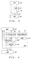
- FIG. 3 is shown the basic test circuit of the present invention where the ATE 20 and the MTE 21 are connected to a DUT 22 using a bus 23 of the DUT.
- a switch S1 24 connects the MTE to the bus 23
- the MTE when connected to the bus allows the MTE to perform memory tests on the embedded memory of the DUT in parallel with analog tests performed on the DUT 22 by the ATE 20.
- FIG. 4 is block diagram of the MTE 21 and connectivity between the MTE and the ATE 20 and the DUT 22.
- the ATE 20 communicates coded information to microcontroller 30 of the MTE 21, which comprises the embedded memory size within the DUT, physical configuration of the embedded memory and the chosen test algorithm.
- a flash memory 31 connected to the microcontroller contains the software for the microcontroller 30.
- the flash memory 31 is programmed with a boundary scan port.
- the microcontroller couples microinstructions to the FPGA (field programmable gate array) 32.
- the RAM 33 that is connected to the FPGA is used to contain a map of the embedded memory of the DUT.
- the RAM 33 is preferably implemented using an SRAM, but other random access memories can be used.
- An arbiter function 35 within the FPGA communicates with the ATE 20 to arbitrate the use of the bus 23 of the DUT 22 and a switch 24 is used to couple the MTE 21 to the bus of the DUT when embedded memory testing is being performed simultaneous to analog testing from the ATE.
- FIG. 5 is a block diagram of the present invention of the logical functions of the MTE.
- the microcontroller 30 generates codes for the state machine 42 and transfers these codes to status registers (SR) 40.
- the address generator 40 generates the next address for testing the embedded memory of the DUT 22 in accordance with the mapping of the embedded memory that is defined in the SR 40.
- the state machine 42 selects an address from the address generator 41 or an increment/decrement address.
- the next address created by the address generator 40 corresponds to the memory mapping provided by the microcontroller 30 and defined in the status registers 40.
- the data generator 43 calculates the correct data word to be applied to the embedded memory of the DUT 22 according to the algorithm supplied by the microcontroller 30 through the status registers 42, and evaluates the test results by comparing the test results to expected values that are dynamically generated. Mismatches between actual measurements and expected values are initially stored in an error buffer and then transferred to the RAM 33 to generate a bit map and image of the tested embedded memory of the DUT 22. This allows the results of the embedded memory test of the DUT 22 to be analyzed later by image processing algorithms to determine failure mechanisms. When a "march test" is performed, the embedded memory bits are first set and then on a separate pass through the embedded memory the memory cells are read and the values read are compared to data calculated by the data generator 43.
- the memory cell location and the value of the error are stored in an error buffer within the FPGA 21. All data read from the embedded memory is stored in a memory map buffer located in the RAM 33.
- a test status flag is set in a status register 40 of the state machine 42.
- the microcontroller 30 couples the test status flag to the ATE 20 to indicate the results of the test of embedded memory within the DUT 22. Besides coupling the test results to the ATE, the microcontroller 30 is capable of coupling to the ATE 20 defective memory cells to provide information for possible repair actions.
- FIG. 6 is a conceptual diagram of the location of the memory test engine (MTE).
- the MTE circuit board 50 is located above the test probe board 51.
- Located under the test probe board 51 are a plurality of test probes 51 that contact a plurality of LCD driver chips 22 simultaneously.
- the test from the ATE 20 and the MTE 21 are applied to the plurality the chips 22 contacted with the plurality of probes 22, simultaneously.
- FIG. 7 is a flow diagram of the method of the present invention for performing both embedded memory testing and analog testing in parallel on an LCD driver chip (DUT).
- DUT LCD driver chip
- MTE memory test engine
- the test of the embedded memory requires that the MTE circuit access the LCD driver chip through the DUT data bus to set up and run the memory tests. Since there is only one data bus emanating from the DUT for use by data and set up, the use of the data bus is arbitrated 61 between the requirements of the memory testing controlled by the MTE circuit and the requirements of analog measurements performed by automatic test equipment (ATE).
- ATE automatic test equipment
- the arbitration of the data bus is a negotiation between the ate and a FPGA (field programmable gate array) located in MTE circuit.
- the memory testing 62 of the embedded memory within the DUT comprises addressing, controlling and providing data to the embedded memory from the MTE, and the embedded memory testing is performed in parallel with the analog testing of the DUT.
- each usage of the data bus is arbitrated 61 between the test functions requiring use of the data bus to resolve conflicts in the usage.
- the register of the DUT is accessed to perform a setup of the DUT to allow analog measurements 63.
- the data bus of the DUT is released 64 to allow usage by subsequent test requirements, either by the analog or the embedded memory testing.
- the analog measurements of the DUT are performed by the ATE 65 while embedded memory tests controlled by the MTE are being performed in parallel. If the analog measurements are not complete 66, the ATE arbitrates with the MTE for the usage of the DUT data bus 61 and repeats the access of the DUT registers through the data bus 63 after which the ATE releases the DUT data bus 64, and analog measurements 65 are performed by the ATE on the DUT. If the analog testing is complete 67, results of the embedded memory tests, which are accumulated in the MTE, are returned from the MTE to the ATE 68.
Landscapes
- Engineering & Computer Science (AREA)
- General Engineering & Computer Science (AREA)
- Physics & Mathematics (AREA)
- General Physics & Mathematics (AREA)
- Computer Networks & Wireless Communication (AREA)
- Tests Of Electronic Circuits (AREA)
- Saccharide Compounds (AREA)
- Techniques For Improving Reliability Of Storages (AREA)
Abstract
Description
- A semiconductor tester and in particular a built-off self test (BOST) for an embedded memory in a device operating simultaneous to other testing being performed.
- Built in self test (BIST) capability occupies valuable real estate on a semiconductor chip especially for implementing a memory BIST. Economics is a prime consideration for semiconductor LCD (liquid crystal display) driver devices. Not only is the real estate that would be occupied with a BIST circuit costly, but also the need to have a tester to perform a set of tests on a semiconductor chip with a diverse set of circuitry is also costly. Testing of such a device requires a sequential set of test procedures in which the testing of the embedded memory occupies a substantial portion of the total test time. Finding ways to reduce the total test time of a device with such a diverse set of requirements is important to the reduction of total product cost.
-
US 6,829,728 (Cheng et al. ) is directed to a test circuit for testing embedded synchronous memories where a BIST (built-in self test) controller is used to address the memory and provide reference data to compare to the memory output.US 6,721,904 (Ernst et al. ) is directed to a BOST (built off (chip) self test) function located between a DUT (device under test) and a semiconductor tester for the purpose of testing a SDRAM.US 6,653,855 (Mori et al. ) is directed to a BOST board containing a connector, a substrate and an external self test circuit. InUS 6,587,979 (Kraus et al. ) a flexible BIST is directed to being incorporated into an integrated circuit chip. InUS 6,286,115 (Stubbs ) discloses a test circuit is directed an on-chip test circuit that includes a multiplexer and an interface to I/O to allow interfacing with I/O associated an embedded memory to allow testing and repairing the embedded memory.US 6,182,257 (Gillingham ) is directed to a semiconductor device with a self test circuit, which includes a test memory array, a self test controller for internally generating test and results data, and an interface for loading test data into the test memory array.US 6,072,737 (Morgan et al. ) is directed to an embedded test circuit to test an embedded DRAM of an integrated circuit chip wherein the test circuitry interfaces with a memory tester. InUS 4,873,705 (Johnson ) a method and system is directed to functionally testing memories in microprocessor based units or boards under test with an interface circuit coupled to the bus structure of the unit under test. - In FIG. 1 is a diagram of prior art showing a test time sequence for testing an LCD driver chip as might be performed by automatic test equipment (ATE). DC tests are first performed as an initial screen of the chip to determine the ability of the chip to be powered and have I/O circuits free of shorts and opens. A test is then performed on the embedded array (RAM) to determine the capability of the array to properly store and read data This is then followed by analog tests to test the ability of the I/O drivers and receivers to function properly, followed by a test of the digital circuits and the chips video capability.
- A built-in-self-test (BIST) circuit could be useful in reducing the test time required by an ATE particularly with respect to the embedded memory, but this would be at the cost of the additional chip size required to accommodate the BIST circuitry and the BIST would require testing. A built-off-(chip)-self test (BOST) could also be used, but an allocation of test time is still required for the embedded memory.
- It is an objective of the present invention to provide an embedded memory test of an LCD driver chip that overlaps analog testing of the chip.
- It is also an objective of the present invention to provide the RAM test of the LCD driver chip that is performed by a MTE (memory test engine) circuit, which is physically mounted on the probe head for the LCD chips.
- It is still an objective of the present invention to probe a plurality of chips to perform chip test on the plurality of chips simultaneously.
- It is further an objective of the present invention to arbitrate the use of the data bus connected to the device under test between the embedded memory test and the analog test to prevent interference between overlapped tests.
- It is still further an objective of the present invention to download test algorithms and array mapping from automatic test equipment (ATE) to the MTE circuitry comprising a microcontroller and a field programmable gate array (FPGA).
- It is also further an objective of the present invention to translate microinstructions from the microcontroller to the FPGA for execution in the embedded array of the LCD driver chip.
- In the present invention an MTE (memory test engine) circuit is mounted above the probe head that is used to contact a plurality of semiconductor chips simultaneously. The MTE circuit receives test instructions from an ATE (automatic test equipment) and converts these instructions into addresses, data and control information to test embedded arrays within the chips contacted by the test probe head. The specific chips under test are LCD driver chips; although, the methodology herein of the present invention is applicable to other chips serving other purposes.
- The LCD driver chips are tested for DC parameters, analog capability of the drivers, logic circuitry surrounding the functions contained on the chip, video capability as well as the capability of the embedded array. The analog testing consumes a substantial amount of time and is separate from the embedded array, which has a different addressing requirement than the driver circuits. This allows the testing of the embedded array to be overlapped in time with the analog testing of the driver circuits and allows the shortening of the total test time for the driver chips.
- An arbiter function within the FPGA in the MTE circuit coordinates the use of the data bus with the ATE to test the LCD chips between the analog testing and the memory testing. Other than the coordination and receiving test instruction from the ATE, the MTE circuit operates independent of the ATE as is done with BIST circuitry embedded within semiconductor chips without occupying valuable semiconductor real estate required by a BIST circuit.
- This invention will be described with reference to the accompanying drawings, wherein:
- FIG. 1 is diagram showing a test sequence time line of prior art;
- FIG. 2 is a diagram showing the test sequence time line of the present invention;
- FIG. 3 is a block diagram of the present invention for the basic test circuitry configuration;
- FIG. 4 is a block diagram of the present invention demonstrating the functions of the MTE circuitry and the interconnectivity to the ATE and a DUT (device under test);
- FIG. 5 is a block diagram of the present invention of the logical functions of the MTE;
- FIG. 6 is a conceptual diagram of the physical location of the MTE circuitry above a chip probe head of the present invention; and
- FIG. 7 is a flow diagram of the present invention for performing memory testing and analog testing simultaneous.
- In FIG. 2 is a test time sequence of the present invention for testing an LCD driver chip performed by automatic test equipment (ATE) and a memory test engine (MTE). The MTE is a form of a BOST (built off-chip self test) circuit where the MTE performs memory tests independent of the ATE. DC screening tests are performed first by the ATE in a sequence of tests followed by
analog tests 10 performed by the ATE overlapped by embedded memory (RAM) 11 performed by the MTE circuitry. Digital testing of the logic on the LCD driver chip and the video testing, both performed by the ATE, follow theoverlap testing - In FIG. 3 is shown the basic test circuit of the present invention where the ATE 20 and the MTE 21 are connected to a
DUT 22 using abus 23 of the DUT. Aswitch S1 24 connects the MTE to thebus 23 The MTE when connected to the bus allows the MTE to perform memory tests on the embedded memory of the DUT in parallel with analog tests performed on theDUT 22 by the ATE 20. - In FIG. 4 is block diagram of the MTE 21 and connectivity between the MTE and the ATE 20 and the
DUT 22. The ATE 20 communicates coded information tomicrocontroller 30 of the MTE 21, which comprises the embedded memory size within the DUT, physical configuration of the embedded memory and the chosen test algorithm. Aflash memory 31 connected to the microcontroller contains the software for themicrocontroller 30. Theflash memory 31 is programmed with a boundary scan port. The microcontroller couples microinstructions to the FPGA (field programmable gate array) 32. TheRAM 33 that is connected to the FPGA is used to contain a map of the embedded memory of the DUT. TheRAM 33 is preferably implemented using an SRAM, but other random access memories can be used. An arbiter function 35 within the FPGA communicates with the ATE 20 to arbitrate the use of thebus 23 of theDUT 22 and aswitch 24 is used to couple theMTE 21 to the bus of the DUT when embedded memory testing is being performed simultaneous to analog testing from the ATE. - FIG. 5 is a block diagram of the present invention of the logical functions of the MTE. The
microcontroller 30 generates codes for thestate machine 42 and transfers these codes to status registers (SR) 40. Theaddress generator 40 generates the next address for testing the embedded memory of theDUT 22 in accordance with the mapping of the embedded memory that is defined in the SR 40. In accordance with the embedded memory in theDUT 22, thestate machine 42 selects an address from theaddress generator 41 or an increment/decrement address. The next address created by theaddress generator 40 corresponds to the memory mapping provided by themicrocontroller 30 and defined in thestatus registers 40. - The
data generator 43 calculates the correct data word to be applied to the embedded memory of theDUT 22 according to the algorithm supplied by themicrocontroller 30 through the status registers 42, and evaluates the test results by comparing the test results to expected values that are dynamically generated. Mismatches between actual measurements and expected values are initially stored in an error buffer and then transferred to theRAM 33 to generate a bit map and image of the tested embedded memory of theDUT 22. This allows the results of the embedded memory test of theDUT 22 to be analyzed later by image processing algorithms to determine failure mechanisms. When a "march test" is performed, the embedded memory bits are first set and then on a separate pass through the embedded memory the memory cells are read and the values read are compared to data calculated by thedata generator 43. - When a test error occurs, the memory cell location and the value of the error are stored in an error buffer within the
FPGA 21. All data read from the embedded memory is stored in a memory map buffer located in theRAM 33. A test status flag is set in astatus register 40 of thestate machine 42. Themicrocontroller 30 couples the test status flag to the ATE 20 to indicate the results of the test of embedded memory within theDUT 22. Besides coupling the test results to the ATE, themicrocontroller 30 is capable of coupling to the ATE 20 defective memory cells to provide information for possible repair actions. - In FIG. 6 is a conceptual diagram of the location of the memory test engine (MTE). The
MTE circuit board 50 is located above thetest probe board 51. Located under thetest probe board 51 are a plurality oftest probes 51 that contact a plurality ofLCD driver chips 22 simultaneously. The test from the ATE 20 and theMTE 21 are applied to the plurality thechips 22 contacted with the plurality ofprobes 22, simultaneously. This requires theRAM 33 connected to thedata generator 43 to be large enough to contain memory maps of the plurality ofchips 22 being simultaneously tested. - FIG. 7 is a flow diagram of the method of the present invention for performing both embedded memory testing and analog testing in parallel on an LCD driver chip (DUT). After a DUT has been tested for catastrophic failures and has been found not to have a catastrophic failure, a test of an embedded memory within the DUT is initiated 60 using the memory test engine (MTE) located in the probe head. The test of the embedded memory requires that the MTE circuit access the LCD driver chip through the DUT data bus to set up and run the memory tests. Since there is only one data bus emanating from the DUT for use by data and set up, the use of the data bus is arbitrated 61 between the requirements of the memory testing controlled by the MTE circuit and the requirements of analog measurements performed by automatic test equipment (ATE). The arbitration of the data bus is a negotiation between the ate and a FPGA (field programmable gate array) located in MTE circuit. The
memory testing 62 of the embedded memory within the DUT comprises addressing, controlling and providing data to the embedded memory from the MTE, and the embedded memory testing is performed in parallel with the analog testing of the DUT. When either the memory testing or the analog testing requires usage of the data bus of the DUT, each usage of the data bus is arbitrated 61 between the test functions requiring use of the data bus to resolve conflicts in the usage. - Continuing to refer to FIG. 7, upon arbitration of the
data bus 61, the register of the DUT is accessed to perform a setup of the DUT to allowanalog measurements 63. Once the setup is complete, the data bus of the DUT is released 64 to allow usage by subsequent test requirements, either by the analog or the embedded memory testing. The analog measurements of the DUT are performed by the ATE 65 while embedded memory tests controlled by the MTE are being performed in parallel. If the analog measurements are not complete 66, the ATE arbitrates with the MTE for the usage of theDUT data bus 61 and repeats the access of the DUT registers through thedata bus 63 after which the ATE releases theDUT data bus 64, andanalog measurements 65 are performed by the ATE on the DUT. If the analog testing is complete 67, results of the embedded memory tests, which are accumulated in the MTE, are returned from the MTE to the ATE 68. - While the invention has been particularly shown and described with reference to preferred embodiments thereof, it will be understood by those skilled in the art that various changes in form and details may be made without departing from the spirit and scope of the invention.
Claims (25)
- A test circuit, comprising:a) an ATE (automatic test equipment);b) a MTE (memory test engine) circuit;c) a device test probe;d) said MTE circuit mounted above said chip test probe and coupled to a DUT (device under test) through said device test probe; ande) said ATE coupled to said DUT through said test probe to perform tests on said DUT and coupled to said MTE circuit to provide test instructions whereby said MTE circuit carries out a sequence of tests on said DUT in parallel with test from said ATE.
- The test circuit of claim 1, wherein said MTE circuit coordinates parallel testing of said DUT with the ATE.
- The test circuit of claim 2, wherein said coordination of the parallel testing is coordination of the use of a test bus connected to said DUT.
- The test circuit of claim 1, wherein said MTE circuit performs tests on an embedded array of said DUT in parallel to analog tests performed by said ATE.
- The test circuit of claim 1, wherein said MTE circuit further comprises a microcontroller, a FPGA (field programmable gate array), a flash memory, a random access memory and a switch.
- The test circuit of claim 5, wherein said microcontroller interfaces with said ATE and to receive code information about said DUT and transfers microinstructions to said FPGA.
- The test circuit of claim 5, wherein said FPGA provides addresses, data and control to the DUT and provides a coordinated use of a test bus connected to said DUT and used by both the ATE and the MTE circuit.
- The test circuit of claim 5, wherein said switch disconnects said MTE circuit from the device test probes.
- The test circuit of claim 1, wherein said device test probe contacts a plurality of DUT's simultaneously to test said plurality of DUT's in parallel.
- The test circuit of claim 1, wherein said DUT is an LCD (liquid crystal display) driver chip containing an embedded memory.
- An external test circuit, comprising:a) a means to couple an ATE (automatic test equipment) and a MTE (memory test engine) circuit to a same DUT (device under test);c) a means to instruct said MTE circuit and allow said MTE circuit to perform tests independent of the ATE;d) a means to share the use of a data bus of said DUT between said ATE and said MTE circuit; ande) a means to overlap a test from said ATE with a test from said BOST circuit.
- The test circuit of claim 11, wherein said means to couple the ATE and the BOST circuit to the same DUT uses said data bus of the DUT wherein the BOST circuit is disconnected from the data bus when the BOST circuit is not being used.
- The test circuit of claim 11, wherein said means to instruct said MTE circuit is provided to the MTE circuit from the ATE and further comprises:a) a size of an embedded memory within said DUT;b) a physical memory configuration of said embedded memory;c) a pin configuration of said DUT;d) a test algorithm; ande) a microcontroller within said MTE circuit receives the instructions from the ATE and connects microinstructions to a FPGA (field programmable gate array) within the MTE circuit that are executed by the FPGA to perform tests of said embedded memory in the DUT, receive back test results from said embedded memory and compare said test results to an expected value.
- The test circuit of claim 11, wherein said means to share the use of a data bus of said DUT between said ATE and said MTE circuit comprises arbitration of the use of said data bus.
- The test circuit of claim 11, wherein said means to overlap a test from said ATE with a test from said MTE circuit overlaps an analog test performed by said ATE with a memory test performed by said MTE circuit.
- The test circuit of claim 15, wherein analog tests and said memory tests use separate DUT addressing.
- The test circuit of claim 15 wherein said MTE circuit provides addresses, data and control of the embedded memory of the DUT and receives back from said DUT test results that are compared in the MTE circuit to expected test results.
- The test circuit of claim 11, wherein said DUT is an LCD driver chip that contains an embedded memory.
- A method for performing tests in parallel, comprising:a) initiating an embedded memory test of a DUT (device under test) using an MTE (memory test engine) mounted on a test probe head for contacting said DUT;b) performing said embedded memory test controlled by said MTE using a data bus of said DUT;c) arbitrating usage of said data bus when initiating analog measurements of said DUT in parallel with said embedded memory tests to prevent conflicts between test functions;d) accessing a register of said DUT to setup analog measurements;e) releasing said usage of the data bus;f) performing analog measurements on the DUT with an ATE (automatic test equipment);g) arbitrating usage of the data bus and repeating steps c) through f) until analog testing is complete; andh) coupling memory test results from said MTE circuit to said ATE upon completion of testing.
- The method of claim 19, wherein initiating tests of the embedded memory couples the MTE circuit to said DUT through data bus.
- The method of claim 19, wherein arbitrating usage of the data bus resolves conflicts between setup of said analog measurements and said embedded memory test.
- The method of claim 19, wherein said arbitrating usage of the data bus of the DUT is conducted between the ATE and a FPGA (field programmable gate array) within said MTE circuit.
- The method of claim 19, wherein performing said embedded memory test further comprises using said data bus for addressing the embedded memory, providing data to the embedded memory, and controlling the embedded memory.
- The method of claim 19, wherein returning embedded memory test results to said MTE circuit allows comparison of the test results to expected values.
- The method of claim 19, wherein the DUT is an LCD driver device.
Priority Applications (4)
| Application Number | Priority Date | Filing Date | Title |
|---|---|---|---|
| DE602006019069T DE602006019069D1 (en) | 2006-05-18 | 2006-05-18 | Test device for memory |
| EP06392009A EP1858028B1 (en) | 2006-05-18 | 2006-05-18 | Memory test engine |
| AT06392009T ATE492885T1 (en) | 2006-05-18 | 2006-05-18 | MEMORY TEST APPARATUS |
| US11/446,625 US7395169B2 (en) | 2006-05-18 | 2006-06-05 | Memory test engine |
Applications Claiming Priority (1)
| Application Number | Priority Date | Filing Date | Title |
|---|---|---|---|
| EP06392009A EP1858028B1 (en) | 2006-05-18 | 2006-05-18 | Memory test engine |
Publications (2)
| Publication Number | Publication Date |
|---|---|
| EP1858028A1 true EP1858028A1 (en) | 2007-11-21 |
| EP1858028B1 EP1858028B1 (en) | 2010-12-22 |
Family
ID=37188933
Family Applications (1)
| Application Number | Title | Priority Date | Filing Date |
|---|---|---|---|
| EP06392009A Expired - Lifetime EP1858028B1 (en) | 2006-05-18 | 2006-05-18 | Memory test engine |
Country Status (4)
| Country | Link |
|---|---|
| US (1) | US7395169B2 (en) |
| EP (1) | EP1858028B1 (en) |
| AT (1) | ATE492885T1 (en) |
| DE (1) | DE602006019069D1 (en) |
Cited By (5)
| Publication number | Priority date | Publication date | Assignee | Title |
|---|---|---|---|---|
| CN106841993A (en) * | 2017-02-16 | 2017-06-13 | 长沙云涯电子科技有限责任公司 | A kind of LCD detection means and method |
| WO2017133185A1 (en) * | 2016-02-02 | 2017-08-10 | 深圳市汇顶科技股份有限公司 | Data acquisition chip test system and device and control method therefor |
| US12099424B2 (en) | 2022-11-10 | 2024-09-24 | Intelligent Memory Limited | Apparatus, systems, and methods for dynamically reconfigured semiconductor tester for volatile and non-volatile memories |
| US12321249B2 (en) | 2022-11-10 | 2025-06-03 | Intelligent Memory Limited | Systems and methods for reducing error log required space in semiconductor testing |
| US12374417B2 (en) | 2022-11-10 | 2025-07-29 | Intelligent Memory Limited | Apparatus, systems, and methods for dynamically reconfigured semiconductor tester for volatile and non-volatile memories |
Families Citing this family (19)
| Publication number | Priority date | Publication date | Assignee | Title |
|---|---|---|---|---|
| US20070127052A1 (en) * | 2005-12-06 | 2007-06-07 | Mediatek Inc. | Electronic recovery system and method |
| US7797598B1 (en) * | 2006-11-14 | 2010-09-14 | Xilinx, Inc. | Dynamic timer for testbench interface synchronization |
| KR20100062326A (en) * | 2008-12-02 | 2010-06-10 | 삼성전자주식회사 | Semiconductor device test apparatus |
| KR101535228B1 (en) * | 2009-05-13 | 2015-07-08 | 삼성전자주식회사 | Built-off test equipment |
| CN101963930B (en) * | 2009-07-21 | 2013-06-12 | 纬创资通股份有限公司 | automated testing device |
| US10162007B2 (en) * | 2013-02-21 | 2018-12-25 | Advantest Corporation | Test architecture having multiple FPGA based hardware accelerator blocks for testing multiple DUTs independently |
| US9952276B2 (en) | 2013-02-21 | 2018-04-24 | Advantest Corporation | Tester with mixed protocol engine in a FPGA block |
| US12079098B2 (en) * | 2013-02-21 | 2024-09-03 | Advantest Corporation | Automated test equipment with hardware accelerator |
| US10161993B2 (en) * | 2013-02-21 | 2018-12-25 | Advantest Corporation | Tester with acceleration on memory and acceleration for automatic pattern generation within a FPGA block |
| US11009550B2 (en) | 2013-02-21 | 2021-05-18 | Advantest Corporation | Test architecture with an FPGA based test board to simulate a DUT or end-point |
| US9810729B2 (en) * | 2013-02-28 | 2017-11-07 | Advantest Corporation | Tester with acceleration for packet building within a FPGA block |
| US10126362B2 (en) * | 2014-12-15 | 2018-11-13 | International Business Machines Corporation | Controlling a test run on a device under test without controlling the test equipment testing the device under test |
| US10976361B2 (en) | 2018-12-20 | 2021-04-13 | Advantest Corporation | Automated test equipment (ATE) support framework for solid state device (SSD) odd sector sizes and protection modes |
| US11137910B2 (en) | 2019-03-04 | 2021-10-05 | Advantest Corporation | Fast address to sector number/offset translation to support odd sector size testing |
| US11237202B2 (en) | 2019-03-12 | 2022-02-01 | Advantest Corporation | Non-standard sector size system support for SSD testing |
| US10884847B1 (en) | 2019-08-20 | 2021-01-05 | Advantest Corporation | Fast parallel CRC determination to support SSD testing |
| US11899550B2 (en) | 2020-03-31 | 2024-02-13 | Advantest Corporation | Enhanced auxiliary memory mapped interface test systems and methods |
| KR102902641B1 (en) | 2021-08-11 | 2025-12-23 | 삼성전자주식회사 | Interface board for testing image sensor, test system having the same, and operating methed thereof |
| US12531133B2 (en) | 2022-11-10 | 2026-01-20 | Intelligent Memory Limited | Systems and methods for reducing error log required space at low temperatures |
Citations (11)
| Publication number | Priority date | Publication date | Assignee | Title |
|---|---|---|---|---|
| US4873705A (en) | 1988-01-27 | 1989-10-10 | John Fluke Mfg. Co., Inc. | Method of and system for high-speed, high-accuracy functional testing of memories in microprocessor-based units |
| US6072737A (en) | 1998-08-06 | 2000-06-06 | Micron Technology, Inc. | Method and apparatus for testing embedded DRAM |
| US6182257B1 (en) | 1997-07-31 | 2001-01-30 | Mosaid Technologies Incorporated | BIST memory test system |
| US6286115B1 (en) | 1998-06-29 | 2001-09-04 | Micron Technology, Inc. | On-chip testing circuit and method for integrated circuits |
| US6331770B1 (en) * | 2000-04-12 | 2001-12-18 | Advantest Corp. | Application specific event based semiconductor test system |
| US20030074153A1 (en) * | 2001-10-15 | 2003-04-17 | Shigeru Sugamori | Application specific event based semiconductor memory test system |
| US6587979B1 (en) | 1999-10-18 | 2003-07-01 | Credence Systems Corporation | Partitionable embedded circuit test system for integrated circuit |
| US6653855B2 (en) | 2001-02-08 | 2003-11-25 | Mitsubishi Denki Kabushiki Kaisha | External test auxiliary device to be used for testing semiconductor device |
| US6721904B2 (en) | 2000-07-18 | 2004-04-13 | Infineon Technologies Ag | System for testing fast integrated digital circuits, in particular semiconductor memory modules |
| US6829728B2 (en) | 2000-11-13 | 2004-12-07 | Wu-Tung Cheng | Full-speed BIST controller for testing embedded synchronous memories |
| US20050058077A1 (en) * | 2003-06-30 | 2005-03-17 | Infineon Technologies Ag | Fast-path implementation for an uplink double tagging engine |
Family Cites Families (4)
| Publication number | Priority date | Publication date | Assignee | Title |
|---|---|---|---|---|
| US4481627A (en) * | 1981-10-30 | 1984-11-06 | Honeywell Information Systems Inc. | Embedded memory testing method and apparatus |
| US6449741B1 (en) * | 1998-10-30 | 2002-09-10 | Ltx Corporation | Single platform electronic tester |
| EP1345197A1 (en) * | 2002-03-11 | 2003-09-17 | Dialog Semiconductor GmbH | LCD module identification |
| US8581610B2 (en) * | 2004-04-21 | 2013-11-12 | Charles A Miller | Method of designing an application specific probe card test system |
-
2006
- 2006-05-18 DE DE602006019069T patent/DE602006019069D1/en not_active Expired - Lifetime
- 2006-05-18 EP EP06392009A patent/EP1858028B1/en not_active Expired - Lifetime
- 2006-05-18 AT AT06392009T patent/ATE492885T1/en not_active IP Right Cessation
- 2006-06-05 US US11/446,625 patent/US7395169B2/en not_active Expired - Fee Related
Patent Citations (11)
| Publication number | Priority date | Publication date | Assignee | Title |
|---|---|---|---|---|
| US4873705A (en) | 1988-01-27 | 1989-10-10 | John Fluke Mfg. Co., Inc. | Method of and system for high-speed, high-accuracy functional testing of memories in microprocessor-based units |
| US6182257B1 (en) | 1997-07-31 | 2001-01-30 | Mosaid Technologies Incorporated | BIST memory test system |
| US6286115B1 (en) | 1998-06-29 | 2001-09-04 | Micron Technology, Inc. | On-chip testing circuit and method for integrated circuits |
| US6072737A (en) | 1998-08-06 | 2000-06-06 | Micron Technology, Inc. | Method and apparatus for testing embedded DRAM |
| US6587979B1 (en) | 1999-10-18 | 2003-07-01 | Credence Systems Corporation | Partitionable embedded circuit test system for integrated circuit |
| US6331770B1 (en) * | 2000-04-12 | 2001-12-18 | Advantest Corp. | Application specific event based semiconductor test system |
| US6721904B2 (en) | 2000-07-18 | 2004-04-13 | Infineon Technologies Ag | System for testing fast integrated digital circuits, in particular semiconductor memory modules |
| US6829728B2 (en) | 2000-11-13 | 2004-12-07 | Wu-Tung Cheng | Full-speed BIST controller for testing embedded synchronous memories |
| US6653855B2 (en) | 2001-02-08 | 2003-11-25 | Mitsubishi Denki Kabushiki Kaisha | External test auxiliary device to be used for testing semiconductor device |
| US20030074153A1 (en) * | 2001-10-15 | 2003-04-17 | Shigeru Sugamori | Application specific event based semiconductor memory test system |
| US20050058077A1 (en) * | 2003-06-30 | 2005-03-17 | Infineon Technologies Ag | Fast-path implementation for an uplink double tagging engine |
Non-Patent Citations (2)
| Title |
|---|
| NIKILA K ET AL.: "DFT for test optimizations in a complex mixed-signal SOC - case study on TI's TNETD7300 ADSL modem device", TEST, 2004 INTEMATIONAL CONFERENCE, 26 October 2004 (2004-10-26), pages 773 - 782 |
| NIKILA K ET AL: "DFT for test optimisations in a complex mixed-signal SOC - case study on TI's TNETD7300 ADSL modem device", TEST, 2004 INTERNATIONAL CONFERCE ON. CHARLOTTE, NC OCT. 26-28, 2004, PISCATAWAY, NJ, USA,IEEE, 26 October 2004 (2004-10-26), pages 773 - 782, XP010763683, ISBN: 0-7803-8580-2 * |
Cited By (7)
| Publication number | Priority date | Publication date | Assignee | Title |
|---|---|---|---|---|
| WO2017133185A1 (en) * | 2016-02-02 | 2017-08-10 | 深圳市汇顶科技股份有限公司 | Data acquisition chip test system and device and control method therefor |
| CN106841993A (en) * | 2017-02-16 | 2017-06-13 | 长沙云涯电子科技有限责任公司 | A kind of LCD detection means and method |
| CN106841993B (en) * | 2017-02-16 | 2019-09-06 | 泰州镭昇光电科技有限公司 | An LCD detection device and method |
| US12099424B2 (en) | 2022-11-10 | 2024-09-24 | Intelligent Memory Limited | Apparatus, systems, and methods for dynamically reconfigured semiconductor tester for volatile and non-volatile memories |
| US12174717B2 (en) | 2022-11-10 | 2024-12-24 | Intelligent Memory Limited | Apparatus, systems, and methods for dynamically reconfigured semiconductor tester for volatile and non-volatile memories |
| US12321249B2 (en) | 2022-11-10 | 2025-06-03 | Intelligent Memory Limited | Systems and methods for reducing error log required space in semiconductor testing |
| US12374417B2 (en) | 2022-11-10 | 2025-07-29 | Intelligent Memory Limited | Apparatus, systems, and methods for dynamically reconfigured semiconductor tester for volatile and non-volatile memories |
Also Published As
| Publication number | Publication date |
|---|---|
| US20070271059A1 (en) | 2007-11-22 |
| US7395169B2 (en) | 2008-07-01 |
| ATE492885T1 (en) | 2011-01-15 |
| DE602006019069D1 (en) | 2011-02-03 |
| EP1858028B1 (en) | 2010-12-22 |
Similar Documents
| Publication | Publication Date | Title |
|---|---|---|
| US7395169B2 (en) | Memory test engine | |
| TWI225199B (en) | Hierarchical test methodology for multi-core chips | |
| US9557366B2 (en) | Tester to simultaneously test different types of semiconductor devices and test system including the same | |
| US6587979B1 (en) | Partitionable embedded circuit test system for integrated circuit | |
| US8170828B2 (en) | Test method using memory programmed with tests and protocol to communicate between device under test and tester | |
| JP4298960B2 (en) | Trigger signal generation method in algorithmically programmable memory tester | |
| US20020133771A1 (en) | On-chip method and apparatus for testing semiconductor circuits | |
| US9640279B1 (en) | Apparatus and method for built-in test and repair of 3D-IC memory | |
| CN111124768B (en) | Method and apparatus for accessing high-capacity test data via a high-speed interface | |
| TWI389129B (en) | Intergrated circuit device | |
| US20080235537A1 (en) | System and method for electronic testing of multiple memory devices | |
| JP2002189632A (en) | Error-trapping RAM for memory testers with SDRAM memory sets configurable with respect to size and speed | |
| JP2004522169A (en) | Electronic circuit optimal parallel inspection access method and apparatus | |
| JP2002267721A (en) | Test apparatus and method for CPU embedded RAM embedded LSI | |
| US7610528B2 (en) | Configuring flash memory | |
| US20120198292A1 (en) | Test apparatus and test method | |
| JP4334463B2 (en) | Semiconductor integrated circuit test apparatus and method | |
| EP0961936B1 (en) | Semiconductor tester with data serializer | |
| JP4334285B2 (en) | Semiconductor test apparatus and control method thereof | |
| US20140164856A1 (en) | pBIST ENGINE WITH REDUCED SRAM TESTING BUS WIDTH | |
| US8368418B2 (en) | Testing apparatus for multiple identical circuit components | |
| US20100096629A1 (en) | Multi-chip module for automatic failure analysis | |
| US7249295B2 (en) | Test circuit for semiconductor device | |
| JP2002203398A (en) | How to avoid wasting time programming with addresses in bad columns | |
| US6311303B1 (en) | Monitor port with selectable trace support |
Legal Events
| Date | Code | Title | Description |
|---|---|---|---|
| PUAI | Public reference made under article 153(3) epc to a published international application that has entered the european phase |
Free format text: ORIGINAL CODE: 0009012 |
|
| AK | Designated contracting states |
Kind code of ref document: A1 Designated state(s): AT BE BG CH CY CZ DE DK EE ES FI FR GB GR HU IE IS IT LI LT LU LV MC NL PL PT RO SE SI SK TR |
|
| AX | Request for extension of the european patent |
Extension state: AL BA HR MK YU |
|
| 17P | Request for examination filed |
Effective date: 20080521 |
|
| 17Q | First examination report despatched |
Effective date: 20080620 |
|
| AKX | Designation fees paid |
Designated state(s): AT BE BG CH CY CZ DE DK EE ES FI FR GB GR HU IE IS IT LI LT LU LV MC NL PL PT RO SE SI SK TR |
|
| GRAP | Despatch of communication of intention to grant a patent |
Free format text: ORIGINAL CODE: EPIDOSNIGR1 |
|
| GRAS | Grant fee paid |
Free format text: ORIGINAL CODE: EPIDOSNIGR3 |
|
| GRAA | (expected) grant |
Free format text: ORIGINAL CODE: 0009210 |
|
| AK | Designated contracting states |
Kind code of ref document: B1 Designated state(s): AT BE BG CH CY CZ DE DK EE ES FI FR GB GR HU IE IS IT LI LT LU LV MC NL PL PT RO SE SI SK TR |
|
| REG | Reference to a national code |
Ref country code: GB Ref legal event code: FG4D |
|
| REG | Reference to a national code |
Ref country code: CH Ref legal event code: EP |
|
| REG | Reference to a national code |
Ref country code: IE Ref legal event code: FG4D |
|
| REF | Corresponds to: |
Ref document number: 602006019069 Country of ref document: DE Date of ref document: 20110203 Kind code of ref document: P |
|
| REG | Reference to a national code |
Ref country code: DE Ref legal event code: R096 Ref document number: 602006019069 Country of ref document: DE Effective date: 20110203 |
|
| REG | Reference to a national code |
Ref country code: NL Ref legal event code: VDEP Effective date: 20101222 |
|
| PG25 | Lapsed in a contracting state [announced via postgrant information from national office to epo] |
Ref country code: LT Free format text: LAPSE BECAUSE OF FAILURE TO SUBMIT A TRANSLATION OF THE DESCRIPTION OR TO PAY THE FEE WITHIN THE PRESCRIBED TIME-LIMIT Effective date: 20101222 |
|
| LTIE | Lt: invalidation of european patent or patent extension |
Effective date: 20101222 |
|
| PG25 | Lapsed in a contracting state [announced via postgrant information from national office to epo] |
Ref country code: AT Free format text: LAPSE BECAUSE OF FAILURE TO SUBMIT A TRANSLATION OF THE DESCRIPTION OR TO PAY THE FEE WITHIN THE PRESCRIBED TIME-LIMIT Effective date: 20101222 Ref country code: BG Free format text: LAPSE BECAUSE OF FAILURE TO SUBMIT A TRANSLATION OF THE DESCRIPTION OR TO PAY THE FEE WITHIN THE PRESCRIBED TIME-LIMIT Effective date: 20110322 Ref country code: LV Free format text: LAPSE BECAUSE OF FAILURE TO SUBMIT A TRANSLATION OF THE DESCRIPTION OR TO PAY THE FEE WITHIN THE PRESCRIBED TIME-LIMIT Effective date: 20101222 Ref country code: FI Free format text: LAPSE BECAUSE OF FAILURE TO SUBMIT A TRANSLATION OF THE DESCRIPTION OR TO PAY THE FEE WITHIN THE PRESCRIBED TIME-LIMIT Effective date: 20101222 Ref country code: SE Free format text: LAPSE BECAUSE OF FAILURE TO SUBMIT A TRANSLATION OF THE DESCRIPTION OR TO PAY THE FEE WITHIN THE PRESCRIBED TIME-LIMIT Effective date: 20101222 Ref country code: CY Free format text: LAPSE BECAUSE OF FAILURE TO SUBMIT A TRANSLATION OF THE DESCRIPTION OR TO PAY THE FEE WITHIN THE PRESCRIBED TIME-LIMIT Effective date: 20101222 Ref country code: SI Free format text: LAPSE BECAUSE OF FAILURE TO SUBMIT A TRANSLATION OF THE DESCRIPTION OR TO PAY THE FEE WITHIN THE PRESCRIBED TIME-LIMIT Effective date: 20101222 |
|
| PG25 | Lapsed in a contracting state [announced via postgrant information from national office to epo] |
Ref country code: PT Free format text: LAPSE BECAUSE OF FAILURE TO SUBMIT A TRANSLATION OF THE DESCRIPTION OR TO PAY THE FEE WITHIN THE PRESCRIBED TIME-LIMIT Effective date: 20110422 Ref country code: IS Free format text: LAPSE BECAUSE OF FAILURE TO SUBMIT A TRANSLATION OF THE DESCRIPTION OR TO PAY THE FEE WITHIN THE PRESCRIBED TIME-LIMIT Effective date: 20110422 Ref country code: GR Free format text: LAPSE BECAUSE OF FAILURE TO SUBMIT A TRANSLATION OF THE DESCRIPTION OR TO PAY THE FEE WITHIN THE PRESCRIBED TIME-LIMIT Effective date: 20110323 Ref country code: CZ Free format text: LAPSE BECAUSE OF FAILURE TO SUBMIT A TRANSLATION OF THE DESCRIPTION OR TO PAY THE FEE WITHIN THE PRESCRIBED TIME-LIMIT Effective date: 20101222 Ref country code: ES Free format text: LAPSE BECAUSE OF FAILURE TO SUBMIT A TRANSLATION OF THE DESCRIPTION OR TO PAY THE FEE WITHIN THE PRESCRIBED TIME-LIMIT Effective date: 20110402 Ref country code: BE Free format text: LAPSE BECAUSE OF FAILURE TO SUBMIT A TRANSLATION OF THE DESCRIPTION OR TO PAY THE FEE WITHIN THE PRESCRIBED TIME-LIMIT Effective date: 20101222 Ref country code: EE Free format text: LAPSE BECAUSE OF FAILURE TO SUBMIT A TRANSLATION OF THE DESCRIPTION OR TO PAY THE FEE WITHIN THE PRESCRIBED TIME-LIMIT Effective date: 20101222 |
|
| PGFP | Annual fee paid to national office [announced via postgrant information from national office to epo] |
Ref country code: FR Payment date: 20110614 Year of fee payment: 6 |
|
| PG25 | Lapsed in a contracting state [announced via postgrant information from national office to epo] |
Ref country code: PL Free format text: LAPSE BECAUSE OF FAILURE TO SUBMIT A TRANSLATION OF THE DESCRIPTION OR TO PAY THE FEE WITHIN THE PRESCRIBED TIME-LIMIT Effective date: 20101222 Ref country code: SK Free format text: LAPSE BECAUSE OF FAILURE TO SUBMIT A TRANSLATION OF THE DESCRIPTION OR TO PAY THE FEE WITHIN THE PRESCRIBED TIME-LIMIT Effective date: 20101222 Ref country code: NL Free format text: LAPSE BECAUSE OF FAILURE TO SUBMIT A TRANSLATION OF THE DESCRIPTION OR TO PAY THE FEE WITHIN THE PRESCRIBED TIME-LIMIT Effective date: 20101222 Ref country code: RO Free format text: LAPSE BECAUSE OF FAILURE TO SUBMIT A TRANSLATION OF THE DESCRIPTION OR TO PAY THE FEE WITHIN THE PRESCRIBED TIME-LIMIT Effective date: 20101222 |
|
| PLBE | No opposition filed within time limit |
Free format text: ORIGINAL CODE: 0009261 |
|
| STAA | Information on the status of an ep patent application or granted ep patent |
Free format text: STATUS: NO OPPOSITION FILED WITHIN TIME LIMIT |
|
| PG25 | Lapsed in a contracting state [announced via postgrant information from national office to epo] |
Ref country code: DK Free format text: LAPSE BECAUSE OF FAILURE TO SUBMIT A TRANSLATION OF THE DESCRIPTION OR TO PAY THE FEE WITHIN THE PRESCRIBED TIME-LIMIT Effective date: 20101222 |
|
| 26N | No opposition filed |
Effective date: 20110923 |
|
| PG25 | Lapsed in a contracting state [announced via postgrant information from national office to epo] |
Ref country code: MC Free format text: LAPSE BECAUSE OF NON-PAYMENT OF DUE FEES Effective date: 20110531 Ref country code: IT Free format text: LAPSE BECAUSE OF FAILURE TO SUBMIT A TRANSLATION OF THE DESCRIPTION OR TO PAY THE FEE WITHIN THE PRESCRIBED TIME-LIMIT Effective date: 20101222 |
|
| REG | Reference to a national code |
Ref country code: CH Ref legal event code: PL |
|
| REG | Reference to a national code |
Ref country code: DE Ref legal event code: R097 Ref document number: 602006019069 Country of ref document: DE Effective date: 20110923 |
|
| PG25 | Lapsed in a contracting state [announced via postgrant information from national office to epo] |
Ref country code: LI Free format text: LAPSE BECAUSE OF NON-PAYMENT OF DUE FEES Effective date: 20110531 Ref country code: CH Free format text: LAPSE BECAUSE OF NON-PAYMENT OF DUE FEES Effective date: 20110531 |
|
| REG | Reference to a national code |
Ref country code: IE Ref legal event code: MM4A |
|
| PG25 | Lapsed in a contracting state [announced via postgrant information from national office to epo] |
Ref country code: IE Free format text: LAPSE BECAUSE OF NON-PAYMENT OF DUE FEES Effective date: 20110518 |
|
| REG | Reference to a national code |
Ref country code: FR Ref legal event code: ST Effective date: 20130131 |
|
| PG25 | Lapsed in a contracting state [announced via postgrant information from national office to epo] |
Ref country code: FR Free format text: LAPSE BECAUSE OF NON-PAYMENT OF DUE FEES Effective date: 20120531 |
|
| PG25 | Lapsed in a contracting state [announced via postgrant information from national office to epo] |
Ref country code: LU Free format text: LAPSE BECAUSE OF NON-PAYMENT OF DUE FEES Effective date: 20110518 |
|
| PG25 | Lapsed in a contracting state [announced via postgrant information from national office to epo] |
Ref country code: TR Free format text: LAPSE BECAUSE OF FAILURE TO SUBMIT A TRANSLATION OF THE DESCRIPTION OR TO PAY THE FEE WITHIN THE PRESCRIBED TIME-LIMIT Effective date: 20101222 |
|
| PG25 | Lapsed in a contracting state [announced via postgrant information from national office to epo] |
Ref country code: HU Free format text: LAPSE BECAUSE OF FAILURE TO SUBMIT A TRANSLATION OF THE DESCRIPTION OR TO PAY THE FEE WITHIN THE PRESCRIBED TIME-LIMIT Effective date: 20101222 |
|
| PGFP | Annual fee paid to national office [announced via postgrant information from national office to epo] |
Ref country code: DE Payment date: 20150513 Year of fee payment: 10 Ref country code: GB Payment date: 20150512 Year of fee payment: 10 |
|
| REG | Reference to a national code |
Ref country code: DE Ref legal event code: R119 Ref document number: 602006019069 Country of ref document: DE |
|
| GBPC | Gb: european patent ceased through non-payment of renewal fee |
Effective date: 20160518 |
|
| PG25 | Lapsed in a contracting state [announced via postgrant information from national office to epo] |
Ref country code: DE Free format text: LAPSE BECAUSE OF NON-PAYMENT OF DUE FEES Effective date: 20161201 |
|
| PG25 | Lapsed in a contracting state [announced via postgrant information from national office to epo] |
Ref country code: GB Free format text: LAPSE BECAUSE OF NON-PAYMENT OF DUE FEES Effective date: 20160518 |