EP1857729A1 - Optoelectronic module and lighting device including the optoelectronic module - Google Patents
Optoelectronic module and lighting device including the optoelectronic module Download PDFInfo
- Publication number
- EP1857729A1 EP1857729A1 EP06425336A EP06425336A EP1857729A1 EP 1857729 A1 EP1857729 A1 EP 1857729A1 EP 06425336 A EP06425336 A EP 06425336A EP 06425336 A EP06425336 A EP 06425336A EP 1857729 A1 EP1857729 A1 EP 1857729A1
- Authority
- EP
- European Patent Office
- Prior art keywords
- radiation
- module according
- cavity
- previous
- substrate
- Prior art date
- Legal status (The legal status is an assumption and is not a legal conclusion. Google has not performed a legal analysis and makes no representation as to the accuracy of the status listed.)
- Granted
Links
- 230000005693 optoelectronics Effects 0.000 title claims abstract description 116
- 230000005855 radiation Effects 0.000 claims abstract description 204
- 230000003287 optical effect Effects 0.000 claims abstract description 59
- 230000008878 coupling Effects 0.000 claims abstract description 3
- 238000010168 coupling process Methods 0.000 claims abstract description 3
- 238000005859 coupling reaction Methods 0.000 claims abstract description 3
- 239000000758 substrate Substances 0.000 claims description 53
- 239000000463 material Substances 0.000 claims description 32
- 238000006243 chemical reaction Methods 0.000 claims description 13
- TZCXTZWJZNENPQ-UHFFFAOYSA-L barium sulfate Chemical compound [Ba+2].[O-]S([O-])(=O)=O TZCXTZWJZNENPQ-UHFFFAOYSA-L 0.000 claims description 10
- OAICVXFJPJFONN-UHFFFAOYSA-N Phosphorus Chemical compound [P] OAICVXFJPJFONN-UHFFFAOYSA-N 0.000 claims description 5
- 239000003086 colorant Substances 0.000 claims description 3
- 229910052698 phosphorus Inorganic materials 0.000 claims 1
- 239000011574 phosphorus Substances 0.000 claims 1
- 239000002184 metal Substances 0.000 description 5
- 229940092690 barium sulfate Drugs 0.000 description 4
- 230000000694 effects Effects 0.000 description 4
- 238000000605 extraction Methods 0.000 description 3
- 239000003973 paint Substances 0.000 description 3
- 238000005538 encapsulation Methods 0.000 description 2
- BHEPBYXIRTUNPN-UHFFFAOYSA-N hydridophosphorus(.) (triplet) Chemical compound [PH] BHEPBYXIRTUNPN-UHFFFAOYSA-N 0.000 description 2
- 238000001228 spectrum Methods 0.000 description 2
- 239000004593 Epoxy Substances 0.000 description 1
- 230000001419 dependent effect Effects 0.000 description 1
- 239000010410 layer Substances 0.000 description 1
- 239000002346 layers by function Substances 0.000 description 1
- 238000004519 manufacturing process Methods 0.000 description 1
- 239000000203 mixture Substances 0.000 description 1
- 230000006798 recombination Effects 0.000 description 1
- 238000005215 recombination Methods 0.000 description 1
- 238000009877 rendering Methods 0.000 description 1
- 239000004065 semiconductor Substances 0.000 description 1
- 238000000926 separation method Methods 0.000 description 1
Images



Classifications
-
- F—MECHANICAL ENGINEERING; LIGHTING; HEATING; WEAPONS; BLASTING
- F21—LIGHTING
- F21K—NON-ELECTRIC LIGHT SOURCES USING LUMINESCENCE; LIGHT SOURCES USING ELECTROCHEMILUMINESCENCE; LIGHT SOURCES USING CHARGES OF COMBUSTIBLE MATERIAL; LIGHT SOURCES USING SEMICONDUCTOR DEVICES AS LIGHT-GENERATING ELEMENTS; LIGHT SOURCES NOT OTHERWISE PROVIDED FOR
- F21K9/00—Light sources using semiconductor devices as light-generating elements, e.g. using light-emitting diodes [LED] or lasers
-
- F—MECHANICAL ENGINEERING; LIGHTING; HEATING; WEAPONS; BLASTING
- F21—LIGHTING
- F21K—NON-ELECTRIC LIGHT SOURCES USING LUMINESCENCE; LIGHT SOURCES USING ELECTROCHEMILUMINESCENCE; LIGHT SOURCES USING CHARGES OF COMBUSTIBLE MATERIAL; LIGHT SOURCES USING SEMICONDUCTOR DEVICES AS LIGHT-GENERATING ELEMENTS; LIGHT SOURCES NOT OTHERWISE PROVIDED FOR
- F21K9/00—Light sources using semiconductor devices as light-generating elements, e.g. using light-emitting diodes [LED] or lasers
- F21K9/60—Optical arrangements integrated in the light source, e.g. for improving the colour rendering index or the light extraction
- F21K9/62—Optical arrangements integrated in the light source, e.g. for improving the colour rendering index or the light extraction using mixing chambers, e.g. housings with reflective walls
-
- F—MECHANICAL ENGINEERING; LIGHTING; HEATING; WEAPONS; BLASTING
- F21—LIGHTING
- F21V—FUNCTIONAL FEATURES OR DETAILS OF LIGHTING DEVICES OR SYSTEMS THEREOF; STRUCTURAL COMBINATIONS OF LIGHTING DEVICES WITH OTHER ARTICLES, NOT OTHERWISE PROVIDED FOR
- F21V7/00—Reflectors for light sources
- F21V7/0025—Combination of two or more reflectors for a single light source
- F21V7/0033—Combination of two or more reflectors for a single light source with successive reflections from one reflector to the next or following
- F21V7/0041—Combination of two or more reflectors for a single light source with successive reflections from one reflector to the next or following for avoiding direct view of the light source or to prevent dazzling
-
- F—MECHANICAL ENGINEERING; LIGHTING; HEATING; WEAPONS; BLASTING
- F21—LIGHTING
- F21V—FUNCTIONAL FEATURES OR DETAILS OF LIGHTING DEVICES OR SYSTEMS THEREOF; STRUCTURAL COMBINATIONS OF LIGHTING DEVICES WITH OTHER ARTICLES, NOT OTHERWISE PROVIDED FOR
- F21V7/00—Reflectors for light sources
- F21V7/0008—Reflectors for light sources providing for indirect lighting
-
- F—MECHANICAL ENGINEERING; LIGHTING; HEATING; WEAPONS; BLASTING
- F21—LIGHTING
- F21V—FUNCTIONAL FEATURES OR DETAILS OF LIGHTING DEVICES OR SYSTEMS THEREOF; STRUCTURAL COMBINATIONS OF LIGHTING DEVICES WITH OTHER ARTICLES, NOT OTHERWISE PROVIDED FOR
- F21V7/00—Reflectors for light sources
- F21V7/04—Optical design
- F21V7/045—Optical design with spherical surface
-
- F—MECHANICAL ENGINEERING; LIGHTING; HEATING; WEAPONS; BLASTING
- F21—LIGHTING
- F21V—FUNCTIONAL FEATURES OR DETAILS OF LIGHTING DEVICES OR SYSTEMS THEREOF; STRUCTURAL COMBINATIONS OF LIGHTING DEVICES WITH OTHER ARTICLES, NOT OTHERWISE PROVIDED FOR
- F21V7/00—Reflectors for light sources
- F21V7/04—Optical design
- F21V7/06—Optical design with parabolic curvature
-
- F—MECHANICAL ENGINEERING; LIGHTING; HEATING; WEAPONS; BLASTING
- F21—LIGHTING
- F21V—FUNCTIONAL FEATURES OR DETAILS OF LIGHTING DEVICES OR SYSTEMS THEREOF; STRUCTURAL COMBINATIONS OF LIGHTING DEVICES WITH OTHER ARTICLES, NOT OTHERWISE PROVIDED FOR
- F21V7/00—Reflectors for light sources
- F21V7/04—Optical design
- F21V7/08—Optical design with elliptical curvature
-
- F—MECHANICAL ENGINEERING; LIGHTING; HEATING; WEAPONS; BLASTING
- F21—LIGHTING
- F21Y—INDEXING SCHEME ASSOCIATED WITH SUBCLASSES F21K, F21L, F21S and F21V, RELATING TO THE FORM OR THE KIND OF THE LIGHT SOURCES OR OF THE COLOUR OF THE LIGHT EMITTED
- F21Y2113/00—Combination of light sources
- F21Y2113/10—Combination of light sources of different colours
- F21Y2113/13—Combination of light sources of different colours comprising an assembly of point-like light sources
-
- F—MECHANICAL ENGINEERING; LIGHTING; HEATING; WEAPONS; BLASTING
- F21—LIGHTING
- F21Y—INDEXING SCHEME ASSOCIATED WITH SUBCLASSES F21K, F21L, F21S and F21V, RELATING TO THE FORM OR THE KIND OF THE LIGHT SOURCES OR OF THE COLOUR OF THE LIGHT EMITTED
- F21Y2115/00—Light-generating elements of semiconductor light sources
- F21Y2115/10—Light-emitting diodes [LED]
Definitions
- the invention relates to the mixing of radiation emitted by different radiation-emitting sources.
- One embodiment of the present invention meets this need by providing an optoelectronic module according to base claim 1. Further embodiments of the invention are subject of further dependent and independent claims.
- the surface of the cavity reflecting the radiation of the first and second different radiation-emitting sources enables an improved mixing of the radiation, thereby resulting in a more homogenous radiation output through the outlet of the first optical element. Therefore such an optoelectronic module produces a more homogenous radiation output distribution than other optoelectronic modules which do not have such a cavity with a reflecting surface.
- the first and second radiation-emitting sources are spatially separated from one another such a mixing of the radiation can lead to a spreading of the radiation sources over a larger area thereby providing a radiation output reducing or even completely compensating the spatial separation of the radiation sources.
- the complete surface of the cavity is able to reflect the radiation.
- the first and second radiation-emitting sources have a preferred direction of emission of the radiation
- only the parts of the surface of the cavity which are arranged in this preferred direction have to be reflective for the radiation.
- radiation-emitting source denotes any kind of radiation source which is able to emit radiation.
- optoelectronic devices which can emit radiation when a voltage is applied can be considered as radiation-emitting sources.
- This term also covers, for example, fluorescent or phosphorescent materials for example radiation conversion materials, which are able to emit secondary radiation when absorbing a primary radiation for example from an optoelectronic device. This secondary radiation can have a longer wavelength than the primary radiation.
- the first radiation-emitting source is able to emit radiation at a wavelength different to the wavelength of the second radiation-emitting source.
- the mixed radiation outcoupled via the outlet would have a wavelength which is a mixture of both radiations.
- a wavelength which is a mixture of both radiations For example in the case that visible radiation is emitted by both radiation-emitting sources an effective color mixing can take place in such an optoelectronic module.
- the first and second radiation sources are a first and second optoelectronic device.
- an optoelectronic device can be for example, an inorganic semiconductor chip, for example a light-emitting diode (LED).
- the optoelectronic devices also can be organic light-emitting diodes (OLEDs), which in general comprise a first and a second electrode and at least one organic functional semiconducting layer disposed between both electrodes. In the case that a voltage is applied via the first and second electrode, electrons and "holes" are injected into the organic functional layer resulting in an emission of radiation upon recombination of the electrons and the "holes".
- the optoelectronic devices can comprise a certain encapsulation for example epoxy including optical elements (for example lenses, diffusors or reflectors), which can influence the spatial distribution of the emitted radiation of the optoelectronic devices.
- the first radiation source is an optoelectronic device and the second radiation source is a radiation conversion material.
- a radiation conversion material is, for example, able to emit radiation at a second wavelength when stimulated by the radiation of the first radiation source (optoelectronic device).
- the radiation emitted by the radiation conversion material has a longer wavelength than the wavelength of the radiation emitted by the optoelectronic device.
- the optoelectronic device can be able to emit blue radiation and the radiation conversion material, for example, phosphorous, can be able to emit yellow radiation when being stimulated by the blue light of the optoelectronic device.
- an effective mixing of the blue and yellow light can take place within the cavity of the first optical element of the optoelectronic module, thereby leading to a white light output through the outlet (see for example Figure 4).
- the optoelectronic devices and radiation sources of the optoelectronic module can be arranged within the cavity of the first optical element.
- the radiation conversion material can be included in the surface of the cavity.
- Such an arrangement of the optoelectronic device and the radiation conversion material can lead to an improved mixing of both radiations due to the fact that parts of the radiation of the optoelectronic device are reflected by the cavities and other parts of the radiation are absorbed by the radiation conversion material.
- a third radiation source is present apart from the first and second radiation source, wherein the third radiation source is able to emit radiation at a wavelength different to the wavelength of the first and second radiation sources.
- a very effective mixing of the radiations of three different wavelengths can be carried out within the cavity by reflecting and thereby mixing the different radiations.
- the first, second and third radiation source emit different primary colors, for example red, green and blue light
- white output can be generated after mixing the different colors.
- circuitry that drives the three radiation sources independently, so that the intensity of radiation emitted by the different sources can be independently tuned or even separately turned off, thereby enabling a broader spectrum of mixed radiation to be emitted by the optoelectronic module.
- the optoelectronic module further comprises a second optical element arranged outside the cavity on or around the outlet.
- Such a second optical element is advantageously able to modulate the mixed radiation outcoupled via the outlet.
- the second optical element can comprise a reflector which can focus the mixed radiation outcoupled through the outlet in a very small radiation beam angle thereby providing a high radiation intensity in the forward direction.
- the second optical element comprises a lens which could also focus the mixed radiation.
- the first optical element can furthermore be opaque for the radiation of the radiation sources.
- the first optical element can comprise metal, plastic or the like.
- the first optical element can, for example, be a metal cup having a highly reflective surface of the cavity (see embodiments). It is also possible to manufacture the first optical element by forming a cavity in a plastic block.
- the first optical element can also comprise a material which is transparent for the radiation of the radiation sources.
- a reflective, opaque material can be applied on the surface of the cavity thereby enabling a good reflection of the radiation.
- the optoelectronic devices as radiation sources are arranged within the cavity of the first optical element around the outlet.
- Such a special arrangement of the optoelectronic devices ensures that a large fraction of the radiation emitted by the optoelectronic devices is first reflected by the surface of the cavity and therefore mixed before leaving the cavity via the outlet (see for example Figures 2, 3 and 4).
- the first optical element of the optoelectronic module comprises a housing including the cavity with a concave curved surface.
- the surface of the cavity can adopt any kind of concaved curved form, for example parabolic, spherical, hemispherical or an ellipsoidal form.
- a cavity with such a concaved curved surface form can effectively reflect the radiation and thereby provide a good mixing of the radiation.
- At least parts of the surface of the cavity are able to reflect the radiation of the radiation sources at least two times forming a multiple reflection surface.
- a multiple reflection surface is preferably orientated relative to the outlet in such a way that radiation reflected by the multiple reflection surface cannot travel directly through the outlet but first has to be reflected again.
- Certain embodiments of multiple reflection surfaces are, for example, shown in Figures 2, 3 and 4.
- the first optical element further comprises a substrate having an opening as the outlet.
- the substrate with the opening can, for example, easily be arranged in such a way relative to the cavity of the first optical element that a closed cavity is provided for mixing the radiation and housing the radiation sources.
- the radiation sources are arranged on the substrate around the opening as, for example, shown in Figure 2 and Figure 7.
- the substrate with the radiation sources can then be mounted on the cavity of the first optical element thereby forming a closed cavity harboring the radiation sources.
- the radiation output surfaces of these optoelectronic devices are preferably arranged in such a way so that the radiation output surfaces are facing the reflective surface of the cavity. Such an arrangement provides a good reflection of the radiation emitted by the optoelectronic devices as, for example, shown in Figures 2, 3 and 4.
- connection member can, for example, also comprise a reflecting surface aligning with the reflecting surface of the cavity and thereby forming a larger reflecting surface.
- the connection member does not necessarily have to comprise a reflecting surface, but can for example also comprise any other non-reflecting material.
- the radiation sources comprise radiation output surfaces defining a main direction for emitting the radiation and the cavity has a concave curved surface with a vertex.
- the radiation output surfaces of the radiation sources are preferably orientated towards the vertex (see for example Fig. 2).
- Radiation output surfaces for defining a main beam direction of the emitted radiation can for example be implemented in optoelectronic devices as radiation sources by including optical elements in the encapsulation of the optoelectronic devices, for example lenses or reflectors, which modulate the emitted radiation. In such a configuration the emitted radiation can effectively be mixed and focused in the vertex of the cavity, thereby enabling a high output of mixed radiation through the outlet.
- the surface of this substrate is preferably tilted towards the opening.
- Such an arrangement is, for example, shown in Figure 2. Due to the tilted surface of the substrate the optoelectronic devices arranged on this surface are also tilted towards the opening of the substrate.
- Such an arrangement can, for example, provide a better radiation mixing due to the fact that the radiation beam paths of the optoelectronic devices can overlap.
- the tilting of the radiation output surfaces of the opto-electronic devices towards the vertex of the cavity can also provide a better outcoupling of the mixed radiation through the opening in the case that the opening is arranged in or near the focal point, where the reflected and mixed radiation is focused (see for example Fig. 2). Then most of the radiation emitted by the optoelectronic devices is reflected and mixed by the vertex of the concaved curved cavity and is therefore focused in or near the focal point of the concave curved cavity for example a parabolic mirror-shaped surface providing a higher radiation output (see for example Figure 2).
- the term "in or near” means that the opening is arranged roughly opposite to the vertex of the parabolic mirror near the focal point.
- outcoupling of the mixed radiation out of the cavity is especially improved when the surface of the substrate on which the optoelectronic devices are arranged is tilted by roughly 30° towards the opening as the outlet.
- the surface area of the substrate on which the optoelectronic devices are arranged is larger than the surface area of that substrate which is directly occupied by the radiation sources as, for example, shown in Figures 2, 3 and 4.
- the additional surface area of the substrate which is free of the optoelectronic devices on the substrate can be made reflective to the radiation emitted by the optoelectronic devices thereby providing an additional reflection surface area.
- This additional surface reflection area is advantageously orientated relative to the outlet of the cavity, so that radiation reflected by that additional reflection radiation surface area is not directly outcoupled through the outlet, but first has to be reflected by other parts of the reflective surface of the cavity before leaving the cavity via the outlet (multiple reflection surface area).
- a closed cavity is formed when the substrate on which the opto-electronic devices are arranged is directly mounted on the cavity of the first optical element.
- a large part of the surface area of the substrate inside the closed cavity which is adjacent to the optoelectronic devices is free of the optoelectronic devices.
- Such configurations are, for example, shown in Figures 2, 3 and 4. These additional surface areas of the substrate which are free of the optoelectronic devices can serve as a multiple reflection surface area thereby improving the mixing of the radiation of the different optoelectronic devices.
- the surface of the cavity may also comprise a diffusive material.
- a diffusive material is able to split the rays of the radiation of the different radiation sources into multiple rays, thereby improving the mixing of the radiation, or example to obtain a good white light mixing starting from an array of selected opto-electronic devices with special wavelengths ( red, green, and blue).
- the surface of the substrate which is free of the optoelectronic devices also comprises a diffusive material as, for example, shown in Figure 3.
- Such a configuration enables a very efficient radiation mixing by reflecting and diffusing the radiation emitted by the optoelectronic devices or other radiation sources, for example radiation conversion materials.
- the diffusive material can comprise a material selected from the group of bariumsulfate and phosphors.
- bariumsulfate as a diffusive material is mixed with white paint in order to improve a better adhesion of the reflective material on the surface of the cavity.
- the bariumsulfate is mixed with 20 to 25 weight percent of white paint in order to ensure good adhesion.
- the phosphorous can additionally convert the radiation emitted by the opto-electronic devices into radiation with a longer wavelength, for example visible light. In the case that UV parts of the radiation emitted by the optoelectronic devices are converted to visible light by the phosphors, the radiation efficiency of the optoelectronic module can be improved.
- the reflecting surface of the cavity can also comprise a faceted surface, which enables a high outcoupling efficiency.
- the optoelectronic devices and the first optical element are thermally conductive connected, so that the heat produced by the optoelectronic devices can easily be transferred away from the optoelectronic devices via the first optical element.
- the substrate on which the optoelectronic devices are arranged is also thermally conductive, the heat produced by the optoelectronic devices can be transferred to the metal cup of the first optical element via the substrate.
- the size of the outlet is variably adjustable, for example by reducing or enlarging the diameter of the opening in the substrate using slits.
- Such a configuration can be used in order to control the intensity of the radiation outcoupled out of the module through the outlet.
- the surface of the cavity may also comprise phosphors.
- This kind of phosphor substrate may be arranged over the substrate of the diffusive material or directly in the cavity structure.
- the effect of this material is used in the fluorescent lamps and in this embodiment the optoelectronic module uses this effect to increase the light extraction from the cavity.
- the phosphors can convert the UV light to visible light.
- the increase of the light extraction from the phosphors is related to the spectrum of the sources; i.e. the lower the wavelength of the source (especially UV light), the higher is the effect of the phosphors.
- the phosphors substrate effect may also increase the CRI (color rendering index) of the white mixed light (starting from optoelectronic R,G,B sources) coming out from the cavity, with respect to CRI of the mixed light without any kind of cavity and phosphor substrate.
- CRI color rendering index
- the cavity structure with phosphors substrate and secondary lens may also be sealed to provide vacuum ambient (inside the cavity) and to give long life to the phosphor substrate.
- the optoelectronic module can form a separate complex part of a larger electronic arrangement. Such a module can formed a self-contained functional unit which can easily be replaced in its entirety.
- the optoelectronic module can be used as a headlamp, for example in automotive applications in any kind of vehicle.
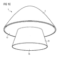
- Figures 1A to 1C show different embodiments of an optoelectronic module in perspective view.
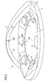
- Figure 2 shows a perspective view of an optoelectronic module with a section cut out of the first optical element.
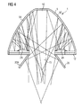
- FIGS 3 and 4 denote different embodiments of the optoelectronic module in cross-sectional view.
- FIGS 5 and 6 show different optoelectronic modules integrated into larger surfaces.
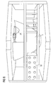
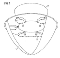
- Figure 7 shows another perspective view of an optoelectronic module in which a section of the reflective mirror of the first optical element is cut out in order to provide insight into the interior of the module.
- Figure 1A shows a perspective view of an optoelectronic module 1 from the side.
- the first optical element 5 comprises a dome-shaped part which can, for example, be made of a metal (metal cup).
- the second optical element 20 is arranged on the first optical element 5 in the form of a reflective tube which is able to focus the radiation outputted via the outlet 15, which is shown in Fig. 1C.
- the dome-shaped first optical element 5 can adopt different forms, for example hemispherical forms as shown in Figure 1B or more parabolic forms as shown in Figure 1A.
- Figure 1C depicts another perspective view of the optoelectronic module where the substrate 12 on which the optoelectronic devices are arranged inside the cavity is shown.
- the substrate 12 also comprises an outlet 15 wherein around the outlet 15 the second optical element 20 is arranged in the form of a tubular-shaped second reflector focusing the radiation outcoupled via the outlet.
- the inventor found out that a diameter of the outlet of roughly 27 mm and a radius of roughly 10 mm of the substrate results in a good mixing and outcoupling efficiency.
- Figure 2 shows another perspective view of the optoelectronic module 1 according to one embodiment of the invention wherein a part of the dome-shaped reflector of the first optical element 5 is cut out in order to provide a view into the interior of the device.
- the second optical element is missing in that figure, but could also be present, for example in the form of a tubular-shaped second reflector as shown in Figure 1A to 1C or even in the form of a lens.
- the first optical element 5 forms a concave-shaped parabolic mirror having a reflective inner surface 5A.
- a substrate 12 on which optoelectronic devices 2A, 2B and 2C are arranged is directly mounted onto the parabolic mirror, thereby forming a closed cavity 10 having an outlet 15.
- the optoelectronic devices only occupy a small fraction of the surface 12A of the substrate 12.
- Parts of that surface 12A which are free of the optoelectronic devices 2A to 2C can also comprise a reflective surface thereby forming a multiple reflection surface area 5B which is able to reflect the radiation beams which were already reflected by the reflecting surface 5A of the dome-shaped optical element.
- the surface 12A of the substrate 12 is tilted towards the outlet 15 so that the radiation output surface areas 4 of the optoelectronic devices 2A to 2C are orientated towards the vertex 30B of the reflective surface 5A of the parabolic mirror of the first optical element 5. In this case more light can be outcoupled through the outlet 15.
- the reflective surface 5A and/or the reflecting surface 12A which is free of the optoelectronic devices 2A to 2C forming the multiple reflection surface area 5B can additionally comprise a diffusive material, for example white paint mixed with bariumsulfate in order to enhance the radiation mixing.
- a diffusive material for example white paint mixed with bariumsulfate in order to enhance the radiation mixing.
- the parabolic mirror of the first optical element 5 is able to focus the radiation of the optoelectronic devices 2A, 2B, 2C in a focal point 30A.
- the outlet 15 is preferably arranged in or near the focal point 30B of the concave mirror thereby improving the outcoupling efficiency of the mixed radiation.
- the optoelectronic devices implemented in the optoelectronic module can for example be the radiation emitting devices described in the patent application WO 02/084749 A2 , which is hereby incorporated by reference in its entirety.
- Figure 3 depicts a cross-sectional schematic view of an optoelectronic module additionally showing the beam paths 3A and 3B of the radiation emitted by the optoelectronic devices 2A and 2B. It can be seen that the radiation 3A, 3B emitted by the optoelectronic devices 2A and 2B can be reflected by the reflecting surface 5A of the parabolic mirror 5 of the first optical element in the cavity 10 before leaving the cavity 10 through the outlet 15. A multiple reflection surface area 5B is present on the substrate 12 on which the optoelectronic devices 2A and 2B are mounted, which is able to reflect radiation beams multiple times before they are coupled out of the cavity 10 through the outlet 15.
- the second optical element 20 again has the form of a tubular-shaped reflector having a reflective inner surface 20A. This reflector is further able to focus the radiation outcoupled out of the module.
- Figure 3 also shows that a large fraction of the radiation 3A, 3B outcoupled out of the cavity 10 is focused in a focal point 30A. Therefore the outlet 15 is preferably arranged in such a way relative to the focal point that most of the light can be outcoupled.
- the reflective mirror surface 5A of the first optical element 5 can optionally additionally comprise diffusive material 40 which can also be present in the multiple reflection surface 5B of the substrate 12.
- Such a diffusive material can enhance the mixing of the radiation of different radiation sources and in case that a phosphor substrate is also present can enhance the light extraction of the radiation of different radiation sources.
- the optoelectronic devices 2A and 2B emit visible radiation of a different wavelength so that the mixing results in a color mixing.
- Figure 4 shows another embodiment of an optoelectronic module 1 according to the invention.
- only two first optoelectronic devices 2A both emitting visible radiation at the same wavelength, but no second optoelectronic devices are present in the cavity 10.
- the parabolic mirror with the reflecting surface 5A of the first optical element 5 also comprises a radiation conversion material 5C able to emit radiation at a longer wavelength than the wavelength of the optoelectronic devices 2A when stimulated by the radiation of the optoelectronic devices.
- a radiation conversion material 5C able to emit radiation at a longer wavelength than the wavelength of the optoelectronic devices 2A when stimulated by the radiation of the optoelectronic devices.
- such a configuration can, for example, be used in order to produce white light output in the case that the first optoelectronic devices 2A emit blue light and the radiation conversion material 5C emits yellow light when absorbing the blue light.
- the parabolic mirror-shaped housing of the first optical element 5 also comprises phosphors on its reflecting surface 5A able to convert invisible UV parts of the radiation emitted by the optoelectronic devices 2A to visible radiation thereby improving the overall light output of the optoelectronic module 1.
- Figures 5 and 6 show different embodiments of the invention where the optoelectronic module is integrated into a larger surface including driver circuits 50 for controlling the module.
- Figure 7 shows a perspective view of an optoelectronic module according to the invention.
Landscapes
- Engineering & Computer Science (AREA)
- General Engineering & Computer Science (AREA)
- Physics & Mathematics (AREA)
- Microelectronics & Electronic Packaging (AREA)
- Optics & Photonics (AREA)
- Led Device Packages (AREA)
Abstract
Description
- The invention relates to the mixing of radiation emitted by different radiation-emitting sources.
- It is the main object of one embodiment of the invention to provide an optoelectronic module with different radiation sources enabling a mixing of the radiation of the different radiation-emitting sources. One embodiment of the present invention meets this need by providing an optoelectronic module according to
base claim 1. Further embodiments of the invention are subject of further dependent and independent claims. - One embodiment of the invention describes an optoelectronic module comprising:
- at least a first and a second radiation-emitting source,
- a first optical element including a cavity, the surface of the cavity able to reflect the radiation of the at least two radiation sources, and
- an outlet in the optical element for coupling radiation out of the cavity,
- wherein the radiation emitted by the radiation sources is reflected by the surface of the cavity and the reflected radiation is outcoupled through the outlet, resulting in a mixing of the radiation from the first and second radiation-emitting source.
- The surface of the cavity reflecting the radiation of the first and second different radiation-emitting sources enables an improved mixing of the radiation, thereby resulting in a more homogenous radiation output through the outlet of the first optical element. Therefore such an optoelectronic module produces a more homogenous radiation output distribution than other optoelectronic modules which do not have such a cavity with a reflecting surface.
- In the case that the first and second radiation-emitting sources are spatially separated from one another such a mixing of the radiation can lead to a spreading of the radiation sources over a larger area thereby providing a radiation output reducing or even completely compensating the spatial separation of the radiation sources.
- It is not necessary that the complete surface of the cavity is able to reflect the radiation. For example, in the case that the first and second radiation-emitting sources have a preferred direction of emission of the radiation, only the parts of the surface of the cavity which are arranged in this preferred direction have to be reflective for the radiation. Preferably more than 90 %, even more preferably more than 95 % of the surface of the cavity should be reflective for the radiation.
- The term "radiation-emitting source" denotes any kind of radiation source which is able to emit radiation. For example optoelectronic devices which can emit radiation when a voltage is applied can be considered as radiation-emitting sources. This term also covers, for example, fluorescent or phosphorescent materials for example radiation conversion materials, which are able to emit secondary radiation when absorbing a primary radiation for example from an optoelectronic device. This secondary radiation can have a longer wavelength than the primary radiation.
- In another embodiment of the invention the first radiation-emitting source is able to emit radiation at a wavelength different to the wavelength of the second radiation-emitting source.
- In such a case the mixed radiation outcoupled via the outlet would have a wavelength which is a mixture of both radiations. For example in the case that visible radiation is emitted by both radiation-emitting sources an effective color mixing can take place in such an optoelectronic module.
- In accordance with another embodiment of the invention the first and second radiation sources are a first and second optoelectronic device. Such an optoelectronic device can be for example, an inorganic semiconductor chip, for example a light-emitting diode (LED). The optoelectronic devices also can be organic light-emitting diodes (OLEDs), which in general comprise a first and a second electrode and at least one organic functional semiconducting layer disposed between both electrodes. In the case that a voltage is applied via the first and second electrode, electrons and "holes" are injected into the organic functional layer resulting in an emission of radiation upon recombination of the electrons and the "holes". The optoelectronic devices can comprise a certain encapsulation for example epoxy including optical elements (for example lenses, diffusors or reflectors), which can influence the spatial distribution of the emitted radiation of the optoelectronic devices.
- It is also possible that according to another embodiment of the invention the first radiation source is an optoelectronic device and the second radiation source is a radiation conversion material. Such a radiation conversion material is, for example, able to emit radiation at a second wavelength when stimulated by the radiation of the first radiation source (optoelectronic device). In some cases the radiation emitted by the radiation conversion material has a longer wavelength than the wavelength of the radiation emitted by the optoelectronic device. For example the optoelectronic device can be able to emit blue radiation and the radiation conversion material, for example, phosphorous, can be able to emit yellow radiation when being stimulated by the blue light of the optoelectronic device. In such a case an effective mixing of the blue and yellow light can take place within the cavity of the first optical element of the optoelectronic module, thereby leading to a white light output through the outlet (see for example Figure 4).
- The optoelectronic devices and radiation sources of the optoelectronic module can be arranged within the cavity of the first optical element.
- Preferably the radiation conversion material can be included in the surface of the cavity. Such an arrangement of the optoelectronic device and the radiation conversion material can lead to an improved mixing of both radiations due to the fact that parts of the radiation of the optoelectronic device are reflected by the cavities and other parts of the radiation are absorbed by the radiation conversion material.
- Furthermore, it is possible that a third radiation source is present apart from the first and second radiation source, wherein the third radiation source is able to emit radiation at a wavelength different to the wavelength of the first and second radiation sources.
- In such a case a very effective mixing of the radiations of three different wavelengths can be carried out within the cavity by reflecting and thereby mixing the different radiations. In the case that the first, second and third radiation source emit different primary colors, for example red, green and blue light, white output can be generated after mixing the different colors. It is also possible to use circuitry that drives the three radiation sources independently, so that the intensity of radiation emitted by the different sources can be independently tuned or even separately turned off, thereby enabling a broader spectrum of mixed radiation to be emitted by the optoelectronic module.
- In yet another embodiment of the invention the optoelectronic module further comprises a second optical element arranged outside the cavity on or around the outlet.
- Such a second optical element is advantageously able to modulate the mixed radiation outcoupled via the outlet. For example the second optical element can comprise a reflector which can focus the mixed radiation outcoupled through the outlet in a very small radiation beam angle thereby providing a high radiation intensity in the forward direction. It is also possible that for example, the second optical element comprises a lens which could also focus the mixed radiation.
- The first optical element can furthermore be opaque for the radiation of the radiation sources. For example, the first optical element can comprise metal, plastic or the like. The first optical element can, for example, be a metal cup having a highly reflective surface of the cavity (see embodiments). It is also possible to manufacture the first optical element by forming a cavity in a plastic block.
- The first optical element can also comprise a material which is transparent for the radiation of the radiation sources. In such an embodiment of the invention a reflective, opaque material can be applied on the surface of the cavity thereby enabling a good reflection of the radiation.
- In yet another embodiment of the invention the optoelectronic devices as radiation sources are arranged within the cavity of the first optical element around the outlet. Such a special arrangement of the optoelectronic devices ensures that a large fraction of the radiation emitted by the optoelectronic devices is first reflected by the surface of the cavity and therefore mixed before leaving the cavity via the outlet (see for example Figures 2, 3 and 4).
- Preferably the first optical element of the optoelectronic module comprises a housing including the cavity with a concave curved surface. The surface of the cavity can adopt any kind of concaved curved form, for example parabolic, spherical, hemispherical or an ellipsoidal form. A cavity with such a concaved curved surface form, as for example shown in Figures 1 and 2, can effectively reflect the radiation and thereby provide a good mixing of the radiation.
- In another embodiment of the invention at least parts of the surface of the cavity are able to reflect the radiation of the radiation sources at least two times forming a multiple reflection surface. Such a multiple reflection surface is preferably orientated relative to the outlet in such a way that radiation reflected by the multiple reflection surface cannot travel directly through the outlet but first has to be reflected again. Certain embodiments of multiple reflection surfaces are, for example, shown in Figures 2, 3 and 4.
- In a further embodiment of the invention the first optical element further comprises a substrate having an opening as the outlet. The substrate with the opening can, for example, easily be arranged in such a way relative to the cavity of the first optical element that a closed cavity is provided for mixing the radiation and housing the radiation sources.
- Advantageously the radiation sources are arranged on the substrate around the opening as, for example, shown in Figure 2 and Figure 7. The substrate with the radiation sources can then be mounted on the cavity of the first optical element thereby forming a closed cavity harboring the radiation sources. When optoelectronic devices are used as radiation sources the radiation output surfaces of these optoelectronic devices are preferably arranged in such a way so that the radiation output surfaces are facing the reflective surface of the cavity. Such an arrangement provides a good reflection of the radiation emitted by the optoelectronic devices as, for example, shown in Figures 2, 3 and 4. Due to the closed cavity and the orientation of the radiation output surfaces of the optoelectronic devices facing the reflective surface of the cavity, the radiation emitted by the optoelectronic devices cannot leave the closed cavity through the opening as the outlet without first being reflected by the reflective surface of the cavity and thereby being mixed with the radiation of the other radiation sources. It is also possible to connect the substrate on which the radiation sources are arranged to the cavity of the housing via a connection member arranged between the substrate and the cavity. Such a connection member can, for example, also comprise a reflecting surface aligning with the reflecting surface of the cavity and thereby forming a larger reflecting surface. The connection member does not necessarily have to comprise a reflecting surface, but can for example also comprise any other non-reflecting material.
- In yet another embodiment of the invention the radiation sources comprise radiation output surfaces defining a main direction for emitting the radiation and the cavity has a concave curved surface with a vertex. In this case the radiation output surfaces of the radiation sources are preferably orientated towards the vertex (see for example Fig. 2). Radiation output surfaces for defining a main beam direction of the emitted radiation can for example be implemented in optoelectronic devices as radiation sources by including optical elements in the encapsulation of the optoelectronic devices, for example lenses or reflectors, which modulate the emitted radiation. In such a configuration the emitted radiation can effectively be mixed and focused in the vertex of the cavity, thereby enabling a high output of mixed radiation through the outlet.
- In the case that the optoelectronic devices are arranged on the surface of the substrate having an opening, the surface of this substrate is preferably tilted towards the opening. Such an arrangement is, for example, shown in Figure 2. Due to the tilted surface of the substrate the optoelectronic devices arranged on this surface are also tilted towards the opening of the substrate. Such an arrangement can, for example, provide a better radiation mixing due to the fact that the radiation beam paths of the optoelectronic devices can overlap.
- The tilting of the radiation output surfaces of the opto-electronic devices towards the vertex of the cavity can also provide a better outcoupling of the mixed radiation through the opening in the case that the opening is arranged in or near the focal point, where the reflected and mixed radiation is focused (see for example Fig. 2). Then most of the radiation emitted by the optoelectronic devices is reflected and mixed by the vertex of the concaved curved cavity and is therefore focused in or near the focal point of the concave curved cavity for example a parabolic mirror-shaped surface providing a higher radiation output (see for example Figure 2). The term "in or near" means that the opening is arranged roughly opposite to the vertex of the parabolic mirror near the focal point. The inventor discovered that outcoupling of the mixed radiation out of the cavity is especially improved when the surface of the substrate on which the optoelectronic devices are arranged is tilted by roughly 30° towards the opening as the outlet.
- Advantageously the surface area of the substrate on which the optoelectronic devices are arranged is larger than the surface area of that substrate which is directly occupied by the radiation sources as, for example, shown in Figures 2, 3 and 4. This means that the additional surface area of the substrate which is free of the optoelectronic devices on the substrate can be made reflective to the radiation emitted by the optoelectronic devices thereby providing an additional reflection surface area. This additional surface reflection area is advantageously orientated relative to the outlet of the cavity, so that radiation reflected by that additional reflection radiation surface area is not directly outcoupled through the outlet, but first has to be reflected by other parts of the reflective surface of the cavity before leaving the cavity via the outlet (multiple reflection surface area).
- According to another embodiment of the invention a closed cavity is formed when the substrate on which the opto-electronic devices are arranged is directly mounted on the cavity of the first optical element. A large part of the surface area of the substrate inside the closed cavity which is adjacent to the optoelectronic devices is free of the optoelectronic devices. Such configurations are, for example, shown in Figures 2, 3 and 4. These additional surface areas of the substrate which are free of the optoelectronic devices can serve as a multiple reflection surface area thereby improving the mixing of the radiation of the different optoelectronic devices.
- In yet another embodiment of the invention the surface of the cavity may also comprise a diffusive material. Such a diffusive material is able to split the rays of the radiation of the different radiation sources into multiple rays, thereby improving the mixing of the radiation, or example to obtain a good white light mixing starting from an array of selected opto-electronic devices with special wavelengths ( red, green, and blue). In the case that a closed cavity is formed by mounting a substrate on which optoelectronic devices are arranged onto the cavity of the first optical element, it is advantageously also possible that the surface of the substrate which is free of the optoelectronic devices also comprises a diffusive material as, for example, shown in Figure 3. Such a configuration enables a very efficient radiation mixing by reflecting and diffusing the radiation emitted by the optoelectronic devices or other radiation sources, for example radiation conversion materials.
- The diffusive material, for example, can comprise a material selected from the group of bariumsulfate and phosphors. Preferably bariumsulfate as a diffusive material is mixed with white paint in order to improve a better adhesion of the reflective material on the surface of the cavity. Preferably the bariumsulfate is mixed with 20 to 25 weight percent of white paint in order to ensure good adhesion. The phosphorous can additionally convert the radiation emitted by the opto-electronic devices into radiation with a longer wavelength, for example visible light. In the case that UV parts of the radiation emitted by the optoelectronic devices are converted to visible light by the phosphors, the radiation efficiency of the optoelectronic module can be improved.
- According to another configuration of the invention, the reflecting surface of the cavity can also comprise a faceted surface, which enables a high outcoupling efficiency.
- Advantageously the optoelectronic devices and the first optical element are thermally conductive connected, so that the heat produced by the optoelectronic devices can easily be transferred away from the optoelectronic devices via the first optical element. For example in the case that the substrate on which the optoelectronic devices are arranged is also thermally conductive, the heat produced by the optoelectronic devices can be transferred to the metal cup of the first optical element via the substrate.
- According to another embodiment of the invention the size of the outlet is variably adjustable, for example by reducing or enlarging the diameter of the opening in the substrate using slits. Such a configuration can be used in order to control the intensity of the radiation outcoupled out of the module through the outlet.
- In one embodiment of the invention the surface of the cavity may also comprise phosphors. This kind of phosphor substrate may be arranged over the substrate of the diffusive material or directly in the cavity structure. The effect of this material is used in the fluorescent lamps and in this embodiment the optoelectronic module uses this effect to increase the light extraction from the cavity. In particular the phosphors can convert the UV light to visible light. The increase of the light extraction from the phosphors is related to the spectrum of the sources; i.e. the lower the wavelength of the source (especially UV light), the higher is the effect of the phosphors. The phosphors substrate effect may also increase the CRI (color rendering index) of the white mixed light (starting from optoelectronic R,G,B sources) coming out from the cavity, with respect to CRI of the mixed light without any kind of cavity and phosphor substrate.
- The cavity structure with phosphors substrate and secondary lens may also be sealed to provide vacuum ambient (inside the cavity) and to give long life to the phosphor substrate.
- The optoelectronic module according to some embodiments of the invention can form a separate complex part of a larger electronic arrangement. Such a module can formed a self-contained functional unit which can easily be replaced in its entirety. The optoelectronic module can be used as a headlamp, for example in automotive applications in any kind of vehicle.
- In the following some embodiments of the invention will be explained in more details by figures and embodiments. All figures are just simplified schematic representations presented for illustration purposes only.
- Figures 1A to 1C show different embodiments of an optoelectronic module in perspective view.
- Figure 2 shows a perspective view of an optoelectronic module with a section cut out of the first optical element.
- Figures 3 and 4 denote different embodiments of the optoelectronic module in cross-sectional view.
- Figures 5 and 6 show different optoelectronic modules integrated into larger surfaces.
- Figure 7 shows another perspective view of an optoelectronic module in which a section of the reflective mirror of the first optical element is cut out in order to provide insight into the interior of the module.
- Figure 1A shows a perspective view of an
optoelectronic module 1 from the side. The firstoptical element 5 comprises a dome-shaped part which can, for example, be made of a metal (metal cup). The secondoptical element 20 is arranged on the firstoptical element 5 in the form of a reflective tube which is able to focus the radiation outputted via theoutlet 15, which is shown in Fig. 1C. The dome-shaped firstoptical element 5 can adopt different forms, for example hemispherical forms as shown in Figure 1B or more parabolic forms as shown in Figure 1A. Figure 1C depicts another perspective view of the optoelectronic module where thesubstrate 12 on which the optoelectronic devices are arranged inside the cavity is shown. Thesubstrate 12 also comprises anoutlet 15 wherein around theoutlet 15 the secondoptical element 20 is arranged in the form of a tubular-shaped second reflector focusing the radiation outcoupled via the outlet. The inventor found out that a diameter of the outlet of roughly 27 mm and a radius of roughly 10 mm of the substrate results in a good mixing and outcoupling efficiency. - Figure 2 shows another perspective view of the
optoelectronic module 1 according to one embodiment of the invention wherein a part of the dome-shaped reflector of the firstoptical element 5 is cut out in order to provide a view into the interior of the device. Furthermore, the second optical element is missing in that figure, but could also be present, for example in the form of a tubular-shaped second reflector as shown in Figure 1A to 1C or even in the form of a lens. It can be seen that the firstoptical element 5 forms a concave-shaped parabolic mirror having a reflectiveinner surface 5A. Asubstrate 12 on whichoptoelectronic devices closed cavity 10 having anoutlet 15. The optoelectronic devices only occupy a small fraction of the surface 12A of thesubstrate 12. Parts of that surface 12A which are free of theoptoelectronic devices 2A to 2C can also comprise a reflective surface thereby forming a multiplereflection surface area 5B which is able to reflect the radiation beams which were already reflected by the reflectingsurface 5A of the dome-shaped optical element. It can be seen that the surface 12A of thesubstrate 12 is tilted towards theoutlet 15 so that the radiationoutput surface areas 4 of theoptoelectronic devices 2A to 2C are orientated towards thevertex 30B of thereflective surface 5A of the parabolic mirror of the firstoptical element 5. In this case more light can be outcoupled through theoutlet 15. Thereflective surface 5A and/or the reflecting surface 12A which is free of theoptoelectronic devices 2A to 2C forming the multiplereflection surface area 5B can additionally comprise a diffusive material, for example white paint mixed with bariumsulfate in order to enhance the radiation mixing. - The parabolic mirror of the first
optical element 5 is able to focus the radiation of theoptoelectronic devices focal point 30A. Theoutlet 15 is preferably arranged in or near thefocal point 30B of the concave mirror thereby improving the outcoupling efficiency of the mixed radiation. - The optoelectronic devices implemented in the optoelectronic module can for example be the radiation emitting devices described in the patent application
WO 02/084749 A2 - Figure 3 depicts a cross-sectional schematic view of an optoelectronic module additionally showing the
beam paths optoelectronic devices radiation optoelectronic devices surface 5A of theparabolic mirror 5 of the first optical element in thecavity 10 before leaving thecavity 10 through theoutlet 15. A multiplereflection surface area 5B is present on thesubstrate 12 on which theoptoelectronic devices cavity 10 through theoutlet 15. The secondoptical element 20 again has the form of a tubular-shaped reflector having a reflectiveinner surface 20A. This reflector is further able to focus the radiation outcoupled out of the module. Figure 3 also shows that a large fraction of theradiation cavity 10 is focused in afocal point 30A. Therefore theoutlet 15 is preferably arranged in such a way relative to the focal point that most of the light can be outcoupled. Thereflective mirror surface 5A of the firstoptical element 5 can optionally additionally comprisediffusive material 40 which can also be present in themultiple reflection surface 5B of thesubstrate 12. As mentioned above such a diffusive material can enhance the mixing of the radiation of different radiation sources and in case that a phosphor substrate is also present can enhance the light extraction of the radiation of different radiation sources. Theoptoelectronic devices - Figure 4 shows another embodiment of an
optoelectronic module 1 according to the invention. In contrast to the embodiment shown in Figure 3, only two firstoptoelectronic devices 2A, both emitting visible radiation at the same wavelength, but no second optoelectronic devices are present in thecavity 10. The parabolic mirror with the reflectingsurface 5A of the firstoptical element 5 also comprises aradiation conversion material 5C able to emit radiation at a longer wavelength than the wavelength of theoptoelectronic devices 2A when stimulated by the radiation of the optoelectronic devices. As mentioned above such a configuration can, for example, be used in order to produce white light output in the case that the firstoptoelectronic devices 2A emit blue light and theradiation conversion material 5C emits yellow light when absorbing the blue light. - It is also possible that the parabolic mirror-shaped housing of the first
optical element 5 also comprises phosphors on its reflectingsurface 5A able to convert invisible UV parts of the radiation emitted by theoptoelectronic devices 2A to visible radiation thereby improving the overall light output of theoptoelectronic module 1. - Figures 5 and 6 show different embodiments of the invention where the optoelectronic module is integrated into a larger surface including
driver circuits 50 for controlling the module. - Figure 7 shows a perspective view of an optoelectronic module according to the invention.
- The scope of protection of the invention is not limited to the examples given hereinabove. The invention is embodied in each novel characteristic and each combination of characteristics, which particularly includes every combination of any features which are stated in the claims, even if this feature or this combination of features is not explicitly stated in the claims or in the examples.
-
- 1
- optoelectronic module
- 2A, 2B, 2C
- radiation sources
- 4
- radiation output surface
- 5
- first optical element
- 5A
- reflecting surface
- 5B
- multiple reflection area
- 10
- cavity
- 11
- substrate
- 12A
- surface of substrate
- 15
- outlet (opening)
- 20
- second optical element
- 30A
- vertex of parabolic mirror
- 30B
- focal point of parabolic mirror
- 40
- diffusive material
- 50
- driver circuit
Claims (34)
- Optoelectronic module (1) comprising:- at least a first (2A) and a second (2B) radiation emitting source,- a first optical element (5) including a cavity (10), the surface (5A) of the cavity (10) able to reflect the radiation (3A, 3B) of the at least two radiation sources (2A, 2B), and- an outlet (15) in the optical element (5) for coupling radiation (3) out of the cavity (10),- wherein the radiation (3) emitted by the radiation sources (2A, 2B) is reflected by the surface (5A) of the cavity (10) and the reflected radiation is out-coupled through the outlet (15), resulting in a mixing of the radiation from the first and second radiation emitting source (2A, 2B).
- Module (1) according to claim 1,- wherein the first radiation emitting source (2A) is able to emit radiation at a wavelength different to the wavelength of the second radiation emitting source (2B).
- Module according to any of the previous claims,- wherein the first and second radiation source (2A, 2B) is a first and second optoelectronic device.
- Module according to any of the claims 1 or 2,- wherein the first radiation source (2A) is an optoelectronic device and the second radiation source (2B) is a radiation conversion material.
- Module according to the previous claim,- wherein said radiation conversion material is included in the surface (5A) of the cavity (10).
- Module according to any of the previous claims, further comprising a third radiation source (2C) arranged within the cavity (10) able to emit radiation at a wavelength different to the wavelength of the first and second optoelectronic devices.
- Module according to the previous claim,- wherein the first, second and third radiation sources are able to emit primary colors.
- Module according to any of the previous claims,- wherein the radiation sources (2A, 2B, 2C) are arranged within the cavity (10).
- Module according to any of the previous claims further comprising- a second optical element (20) arranged outside the cavity (10) on or around the outlet (15).
- Module according to the previous claim,- wherein the second optical element (20) comprises a lens.
- Module according to claim 9,- wherein the second optical element (20) comprises a reflector.
- Module according to any of the previous claims- wherein the first optical element (5) is opaque for the radiation of the radiation sources.
- Module according to any of the previous claims,- wherein optoelectronic devices as radiation sources are arranged within the cavity (10) around the outlet (15).
- Module according to any of the previous claims,- wherein the first optical element (5) comprises a housing including the cavity (10) with a concave curved surface.
- Module according to the previous claim,- wherein the surface (5A) of the cavity (10) is parabolic, spherical, hemispherical or ellipsoidal.
- Module according to any of the previous claims,- wherein at least parts of the surface (5A) are able to reflect the radiation (3A, 3B) of the radiation sources (2A, 2B) at least two-times forming a multiple-reflection surface (5B) .
- Module according to any of the previous claims,- wherein the first optical element further comprises a substrate (12) having an opening as the outlet (15).
- Module according to the previous claim,- wherein the radiation sources (2A, 2B, 2C) are arranged on the substrate (12) around the opening.
- Module according to any of the claims 17 or 18,- wherein the substrate (12) is mounted on the cavity (10) of the first optical element (5) thereby forming a closed cavity.
- Module according to any of the preceding claims, wherein- the radiation sources (2A, 2B, 2C) comprise radiation output surfaces (4) defining a main direction for emitting the radiation,- the cavity has a concave curved surface with a vertex (30B),- the radiation output surfaces (4) of the radiation sources (2A, 2B, 2C) are orientated towards the vertex (30B).
- Module according to the previous claim,- wherein the optoelectronic devices (2A, 2B, 2C) are arranged on the surface (12A) of a substrate (12) with an opening (15) as the outlet, the surface of the substrate is tilted by roughly 30° towards the opening.
- Module according to any of the claims 17 to 21,- wherein the surface (12A) of the substrate (12) is at least partly reflective for the radiation emitted by the radiation sources (2A, 2B, 2C).
- Module according to the previous claim, wherein- the substrate is directly mounted on the cavity of the first optical element thereby forming a closed cavity,- optoelectronic devices as radiation sources are arranged around the opening of the substrate on the substrate,- a large part of the surface area of the substrate inside the closed cavity being adjacent to the housing is free of the optoelectronic devices.
- Module according to any of the claims 17 to 23,- wherein the substrate is flat.
- Module according to any of the claims 17 to 23 further comprising- electronic components for controlling the current of the optoelectronic devices,- the electronic components are arranged on the surface of the substrate remote to the optoelectronic devices.
- Module according to any of the claims 17 to 25,- wherein the substrate is also a driver circuit board.
- Module according to any of the previous claims 1 to 16, further comprising electronic components for controlling the current of the optoelectronic devices.
- Module according to any of the previous claims,- wherein the surface of the cavity also comprises a diffusive material (40).
- Module according to any of the previous claims,- wherein the internal reflecting surface of the cavity comprises a material selected from the group of BaSO4 and phosphorus.
- Module according to any of the previous claims,- wherein the internal reflecting surface of the cavity comprises a faceted surface.
- Module according to any of the previous claims,- wherein the internal surface of the cavity forms a concave mirror able to focus the radiation of the optoelectronic devices in a focal point,- wherein the outlet is arranged in or near the focal point.
- Module according to any of the previous claims,- wherein the optoelectronic devices and the first optical element are thermally conductive connected.
- Module according to any of the previous claims,- Wherein the size of the outlet is variable adjustable.
- Lighting device comprising:- at least one optoelectronic module according to any of the previous claims.
Priority Applications (5)
| Application Number | Priority Date | Filing Date | Title |
|---|---|---|---|
| EP06425336A EP1857729B1 (en) | 2006-05-19 | 2006-05-19 | Optoelectronic module and lighting device including the optoelectronic module |
| AT06425336T ATE450751T1 (en) | 2006-05-19 | 2006-05-19 | OPTOELECTRONIC MODULE AND LIGHTING DEVICE COMPRISING SUCH A MODULE |
| DE602006010826T DE602006010826D1 (en) | 2006-05-19 | 2006-05-19 | Optoelectronic module and lighting device with such a module |
| DE102007015475A DE102007015475A1 (en) | 2006-05-19 | 2007-03-30 | Multiple light emitting diode module |
| US11/798,558 US9042041B2 (en) | 2006-05-19 | 2007-05-15 | Optoelectronic module and lighting device including the optoelectronic module |
Applications Claiming Priority (1)
| Application Number | Priority Date | Filing Date | Title |
|---|---|---|---|
| EP06425336A EP1857729B1 (en) | 2006-05-19 | 2006-05-19 | Optoelectronic module and lighting device including the optoelectronic module |
Publications (2)
| Publication Number | Publication Date |
|---|---|
| EP1857729A1 true EP1857729A1 (en) | 2007-11-21 |
| EP1857729B1 EP1857729B1 (en) | 2009-12-02 |
Family
ID=37546791
Family Applications (1)
| Application Number | Title | Priority Date | Filing Date |
|---|---|---|---|
| EP06425336A Ceased EP1857729B1 (en) | 2006-05-19 | 2006-05-19 | Optoelectronic module and lighting device including the optoelectronic module |
Country Status (4)
| Country | Link |
|---|---|
| US (1) | US9042041B2 (en) |
| EP (1) | EP1857729B1 (en) |
| AT (1) | ATE450751T1 (en) |
| DE (2) | DE602006010826D1 (en) |
Cited By (9)
| Publication number | Priority date | Publication date | Assignee | Title |
|---|---|---|---|---|
| TWI402999B (en) * | 2008-01-14 | 2013-07-21 | Epistar Corp | Light-emitting device |
| JP2013235854A (en) * | 2007-10-17 | 2013-11-21 | Xicato Inc | LIGHTING DEVICE WITH LIGHT EMITTING DIODE |
| GB2504334A (en) * | 2012-07-26 | 2014-01-29 | Sharp Kk | Headlight system with adaptive beams |
| US8931939B2 (en) | 2009-08-20 | 2015-01-13 | Arnold & Richter Cine Tecnik Gmbh & Co. Betriebs Kg | LED luminaire, particularly LED headlight |
| EP2843301A1 (en) * | 2013-08-30 | 2015-03-04 | Danmarks Tekniske Universitet | Light engine for an illumination device |
| US20150131260A1 (en) * | 2012-06-08 | 2015-05-14 | Koninklijke Philips N.V. | Light-emitting device comprising a hollow retro-reflector |
| EP3156720A1 (en) * | 2015-10-15 | 2017-04-19 | GE Lighting Solutions, LLC | An indirect light mixing led module for point-source applications |
| EP3156719A1 (en) * | 2015-10-15 | 2017-04-19 | GE Lighting Solutions, LLC | An indirect color-mixing led module for point-source application |
| US10571082B2 (en) | 2016-10-11 | 2020-02-25 | Signify Holding B.V. | Lighting device for a light source |
Families Citing this family (5)
| Publication number | Priority date | Publication date | Assignee | Title |
|---|---|---|---|---|
| DE102007040873B4 (en) * | 2007-08-29 | 2017-07-20 | Osram Gmbh | Lighting device and method for adjusting a radiation characteristic of a lighting device |
| DE102008031987A1 (en) | 2008-07-07 | 2010-04-15 | Osram Gesellschaft mit beschränkter Haftung | lighting device |
| DE102009047487A1 (en) | 2009-12-04 | 2011-06-09 | Osram Gesellschaft mit beschränkter Haftung | light module |
| DE102010023956A1 (en) * | 2010-06-16 | 2011-12-22 | Osram Opto Semiconductors Gmbh | light source |
| DE102010062463A1 (en) * | 2010-12-06 | 2012-06-06 | Osram Ag | Lighting-device i.e. vehicle headlight, has phosphor regions individually illuminatable by respective light sources, and aligned for diffuse radiation of light on downstream optical elements, which exhibit different optical properties |
Citations (11)
| Publication number | Priority date | Publication date | Assignee | Title |
|---|---|---|---|---|
| US6149283A (en) * | 1998-12-09 | 2000-11-21 | Rensselaer Polytechnic Institute (Rpi) | LED lamp with reflector and multicolor adjuster |
| JP2001243821A (en) * | 2000-02-28 | 2001-09-07 | Mitsubishi Electric Lighting Corp | Surface-emitting LED light source |
| WO2002084749A2 (en) | 2001-04-10 | 2002-10-24 | Osram Opto Semiconductors Gmbh | Conductor frame and housing for a radiation-emitting component, radiation emitting component and method for producing the same |
| JP2003008067A (en) * | 2001-06-27 | 2003-01-10 | Toyoda Gosei Co Ltd | Light-shielding light-emitting diode |
| DE10164033A1 (en) * | 2001-12-28 | 2003-07-10 | Osram Opto Semiconductors Gmbh | Optoelectronic component reflects light from individual sources onto a diffuser which projects a unified virtual light source through a housing window |
| WO2004088200A2 (en) * | 2003-03-31 | 2004-10-14 | Osram Opto Semiconductors Gmbh | Headlight and headlight element |
| US6841804B1 (en) * | 2003-10-27 | 2005-01-11 | Formosa Epitaxy Incorporation | Device of white light-emitting diode |
| US20050135113A1 (en) * | 2003-12-18 | 2005-06-23 | Harvatek Corporation | Optical projection device of a colored lighting module |
| US20050157503A1 (en) * | 2004-01-20 | 2005-07-21 | Chao-Tang Lin | Low-power high-intensity lighting apparatus |
| DE102004013226A1 (en) * | 2004-03-18 | 2005-09-29 | Andreas Friedrich Roithner | LED reflector unit e.g. for vehicle lamp, has LED elements and reflector unit for producing ray of light which is produced exclusively by reflected light by optical opening being uncoupled |
| WO2006033032A1 (en) * | 2004-09-24 | 2006-03-30 | Koninklijke Philips Electronics N.V. | Illumination system |
Family Cites Families (5)
| Publication number | Priority date | Publication date | Assignee | Title |
|---|---|---|---|---|
| US6634759B1 (en) * | 2000-03-27 | 2003-10-21 | Cogent Light Technologies, Inc. | Coupling of light from a light source to a target using dual ellipsoidal reflectors |
| US7447891B2 (en) * | 2003-04-30 | 2008-11-04 | Hewlett-Packard Development Company, L.P. | Light modulator with concentric control-electrode structure |
| US7540629B2 (en) * | 2004-12-28 | 2009-06-02 | General Electric Company | Modular fixture and sports lighting system |
| US7151599B2 (en) * | 2005-01-27 | 2006-12-19 | Hewlett-Packard Development Company, L.P. | Monolithic system and method for enhanced Raman spectroscopy |
| US7923706B2 (en) * | 2008-10-03 | 2011-04-12 | Nordson Corporation | Ultraviolet curing apparatus for continuous material |
-
2006
- 2006-05-19 EP EP06425336A patent/EP1857729B1/en not_active Ceased
- 2006-05-19 DE DE602006010826T patent/DE602006010826D1/en not_active Expired - Lifetime
- 2006-05-19 AT AT06425336T patent/ATE450751T1/en not_active IP Right Cessation
-
2007
- 2007-03-30 DE DE102007015475A patent/DE102007015475A1/en not_active Withdrawn
- 2007-05-15 US US11/798,558 patent/US9042041B2/en not_active Expired - Fee Related
Patent Citations (11)
| Publication number | Priority date | Publication date | Assignee | Title |
|---|---|---|---|---|
| US6149283A (en) * | 1998-12-09 | 2000-11-21 | Rensselaer Polytechnic Institute (Rpi) | LED lamp with reflector and multicolor adjuster |
| JP2001243821A (en) * | 2000-02-28 | 2001-09-07 | Mitsubishi Electric Lighting Corp | Surface-emitting LED light source |
| WO2002084749A2 (en) | 2001-04-10 | 2002-10-24 | Osram Opto Semiconductors Gmbh | Conductor frame and housing for a radiation-emitting component, radiation emitting component and method for producing the same |
| JP2003008067A (en) * | 2001-06-27 | 2003-01-10 | Toyoda Gosei Co Ltd | Light-shielding light-emitting diode |
| DE10164033A1 (en) * | 2001-12-28 | 2003-07-10 | Osram Opto Semiconductors Gmbh | Optoelectronic component reflects light from individual sources onto a diffuser which projects a unified virtual light source through a housing window |
| WO2004088200A2 (en) * | 2003-03-31 | 2004-10-14 | Osram Opto Semiconductors Gmbh | Headlight and headlight element |
| US6841804B1 (en) * | 2003-10-27 | 2005-01-11 | Formosa Epitaxy Incorporation | Device of white light-emitting diode |
| US20050135113A1 (en) * | 2003-12-18 | 2005-06-23 | Harvatek Corporation | Optical projection device of a colored lighting module |
| US20050157503A1 (en) * | 2004-01-20 | 2005-07-21 | Chao-Tang Lin | Low-power high-intensity lighting apparatus |
| DE102004013226A1 (en) * | 2004-03-18 | 2005-09-29 | Andreas Friedrich Roithner | LED reflector unit e.g. for vehicle lamp, has LED elements and reflector unit for producing ray of light which is produced exclusively by reflected light by optical opening being uncoupled |
| WO2006033032A1 (en) * | 2004-09-24 | 2006-03-30 | Koninklijke Philips Electronics N.V. | Illumination system |
Cited By (11)
| Publication number | Priority date | Publication date | Assignee | Title |
|---|---|---|---|---|
| JP2013235854A (en) * | 2007-10-17 | 2013-11-21 | Xicato Inc | LIGHTING DEVICE WITH LIGHT EMITTING DIODE |
| TWI402999B (en) * | 2008-01-14 | 2013-07-21 | Epistar Corp | Light-emitting device |
| US8931939B2 (en) | 2009-08-20 | 2015-01-13 | Arnold & Richter Cine Tecnik Gmbh & Co. Betriebs Kg | LED luminaire, particularly LED headlight |
| US20150131260A1 (en) * | 2012-06-08 | 2015-05-14 | Koninklijke Philips N.V. | Light-emitting device comprising a hollow retro-reflector |
| GB2504334A (en) * | 2012-07-26 | 2014-01-29 | Sharp Kk | Headlight system with adaptive beams |
| US9200780B2 (en) | 2012-07-26 | 2015-12-01 | Sharp Kabushiki Kaisha | Light source for an automotive headlight with adaptive function |
| EP2843301A1 (en) * | 2013-08-30 | 2015-03-04 | Danmarks Tekniske Universitet | Light engine for an illumination device |
| EP3156720A1 (en) * | 2015-10-15 | 2017-04-19 | GE Lighting Solutions, LLC | An indirect light mixing led module for point-source applications |
| EP3156719A1 (en) * | 2015-10-15 | 2017-04-19 | GE Lighting Solutions, LLC | An indirect color-mixing led module for point-source application |
| US10100984B2 (en) | 2015-10-15 | 2018-10-16 | GE Lighting Solutions, LLC | Indirect light mixing LED module for point-source applications |
| US10571082B2 (en) | 2016-10-11 | 2020-02-25 | Signify Holding B.V. | Lighting device for a light source |
Also Published As
| Publication number | Publication date |
|---|---|
| ATE450751T1 (en) | 2009-12-15 |
| US20070268696A1 (en) | 2007-11-22 |
| US9042041B2 (en) | 2015-05-26 |
| DE102007015475A1 (en) | 2008-05-29 |
| DE602006010826D1 (en) | 2010-01-14 |
| EP1857729B1 (en) | 2009-12-02 |
Similar Documents
| Publication | Publication Date | Title |
|---|---|---|
| US9042041B2 (en) | Optoelectronic module and lighting device including the optoelectronic module | |
| JP4729665B2 (en) | Lighting device | |
| US7712922B2 (en) | Illumination unit comprising an LED light source | |
| EP2529421B1 (en) | Light emitting diode device having a wide angular distribution | |
| US8672512B2 (en) | Omni reflective optics for wide angle emission LED light bulb | |
| US9217553B2 (en) | LED lighting systems including luminescent layers on remote reflectors | |
| EP2524165B1 (en) | Apparatus, method to change light source color temperature with reduced optical filtering losses | |
| KR101214135B1 (en) | Light engine | |
| US8071990B2 (en) | Optoelectronic component that emits electromagnetic radiation and illumination module | |
| US7385349B2 (en) | Light emitting module and lighting unit for vehicle | |
| US7812363B2 (en) | Light emitting device module | |
| JP5028466B2 (en) | Car headlights | |
| KR101497482B1 (en) | Lighting module | |
| KR20090026196A (en) | Efficient emitting led package and method for efficiently emitting light | |
| CN1425117A (en) | Solid state lamp | |
| JP2009512151A (en) | Multifunctional automotive floodlight module, especially for the automotive front area | |
| CN102317680A (en) | Lamp cover and LED lamp using the same | |
| JP2006521667A (en) | Light projecting device and light projecting element | |
| CN109479075A (en) | Lighting equipment for mobile terminals | |
| US20150085466A1 (en) | Low profile led-based lighting arrangements | |
| JP2007059864A (en) | LIGHTING DEVICE AND LIGHT EMITTING DIODE DEVICE | |
| US20120162985A1 (en) | Solid state lighting unit incorporating optical spreading elements | |
| JP2022517870A (en) | Light extraction bridge in the cup | |
| CN110748805B (en) | Lighting source system | |
| CN204201685U (en) | Ligthing paraphernalia |
Legal Events
| Date | Code | Title | Description |
|---|---|---|---|
| PUAI | Public reference made under article 153(3) epc to a published international application that has entered the european phase |
Free format text: ORIGINAL CODE: 0009012 |
|
| AK | Designated contracting states |
Kind code of ref document: A1 Designated state(s): AT BE BG CH CY CZ DE DK EE ES FI FR GB GR HU IE IS IT LI LT LU LV MC NL PL PT RO SE SI SK TR |
|
| AX | Request for extension of the european patent |
Extension state: AL BA HR MK YU |
|
| 17P | Request for examination filed |
Effective date: 20080131 |
|
| AKX | Designation fees paid |
Designated state(s): AT BE BG CH CY CZ DE DK EE ES FI FR GB GR HU IE IS IT LI LT LU LV MC NL PL PT RO SE SI SK TR |
|
| RAP1 | Party data changed (applicant data changed or rights of an application transferred) |
Owner name: OSRAM GESELLSCHAFT MIT BESCHRAENKTER HAFTUNG Owner name: OSRAM S.P.A. - SOCIETA' RIUNITE OSRAM EDISON CLERI |
|
| 17Q | First examination report despatched |
Effective date: 20081211 |
|
| GRAP | Despatch of communication of intention to grant a patent |
Free format text: ORIGINAL CODE: EPIDOSNIGR1 |
|
| GRAS | Grant fee paid |
Free format text: ORIGINAL CODE: EPIDOSNIGR3 |
|
| GRAA | (expected) grant |
Free format text: ORIGINAL CODE: 0009210 |
|
| AK | Designated contracting states |
Kind code of ref document: B1 Designated state(s): AT BE BG CH CY CZ DE DK EE ES FI FR GB GR HU IE IS IT LI LT LU LV MC NL PL PT RO SE SI SK TR |
|
| REG | Reference to a national code |
Ref country code: GB Ref legal event code: FG4D |
|
| REG | Reference to a national code |
Ref country code: CH Ref legal event code: EP |
|
| REG | Reference to a national code |
Ref country code: IE Ref legal event code: FG4D |
|
| REF | Corresponds to: |
Ref document number: 602006010826 Country of ref document: DE Date of ref document: 20100114 Kind code of ref document: P |
|
| REG | Reference to a national code |
Ref country code: NL Ref legal event code: VDEP Effective date: 20091202 |
|
| PG25 | Lapsed in a contracting state [announced via postgrant information from national office to epo] |
Ref country code: FI Free format text: LAPSE BECAUSE OF FAILURE TO SUBMIT A TRANSLATION OF THE DESCRIPTION OR TO PAY THE FEE WITHIN THE PRESCRIBED TIME-LIMIT Effective date: 20091202 Ref country code: LT Free format text: LAPSE BECAUSE OF FAILURE TO SUBMIT A TRANSLATION OF THE DESCRIPTION OR TO PAY THE FEE WITHIN THE PRESCRIBED TIME-LIMIT Effective date: 20091202 Ref country code: SE Free format text: LAPSE BECAUSE OF FAILURE TO SUBMIT A TRANSLATION OF THE DESCRIPTION OR TO PAY THE FEE WITHIN THE PRESCRIBED TIME-LIMIT Effective date: 20091202 |
|
| LTIE | Lt: invalidation of european patent or patent extension |
Effective date: 20091202 |
|
| PG25 | Lapsed in a contracting state [announced via postgrant information from national office to epo] |
Ref country code: SI Free format text: LAPSE BECAUSE OF FAILURE TO SUBMIT A TRANSLATION OF THE DESCRIPTION OR TO PAY THE FEE WITHIN THE PRESCRIBED TIME-LIMIT Effective date: 20091202 Ref country code: CY Free format text: LAPSE BECAUSE OF FAILURE TO SUBMIT A TRANSLATION OF THE DESCRIPTION OR TO PAY THE FEE WITHIN THE PRESCRIBED TIME-LIMIT Effective date: 20091202 Ref country code: LV Free format text: LAPSE BECAUSE OF FAILURE TO SUBMIT A TRANSLATION OF THE DESCRIPTION OR TO PAY THE FEE WITHIN THE PRESCRIBED TIME-LIMIT Effective date: 20091202 Ref country code: PL Free format text: LAPSE BECAUSE OF FAILURE TO SUBMIT A TRANSLATION OF THE DESCRIPTION OR TO PAY THE FEE WITHIN THE PRESCRIBED TIME-LIMIT Effective date: 20091202 |
|
| PG25 | Lapsed in a contracting state [announced via postgrant information from national office to epo] |
Ref country code: AT Free format text: LAPSE BECAUSE OF FAILURE TO SUBMIT A TRANSLATION OF THE DESCRIPTION OR TO PAY THE FEE WITHIN THE PRESCRIBED TIME-LIMIT Effective date: 20091202 |
|
| PG25 | Lapsed in a contracting state [announced via postgrant information from national office to epo] |
Ref country code: RO Free format text: LAPSE BECAUSE OF FAILURE TO SUBMIT A TRANSLATION OF THE DESCRIPTION OR TO PAY THE FEE WITHIN THE PRESCRIBED TIME-LIMIT Effective date: 20091202 Ref country code: EE Free format text: LAPSE BECAUSE OF FAILURE TO SUBMIT A TRANSLATION OF THE DESCRIPTION OR TO PAY THE FEE WITHIN THE PRESCRIBED TIME-LIMIT Effective date: 20091202 Ref country code: ES Free format text: LAPSE BECAUSE OF FAILURE TO SUBMIT A TRANSLATION OF THE DESCRIPTION OR TO PAY THE FEE WITHIN THE PRESCRIBED TIME-LIMIT Effective date: 20100313 Ref country code: BG Free format text: LAPSE BECAUSE OF FAILURE TO SUBMIT A TRANSLATION OF THE DESCRIPTION OR TO PAY THE FEE WITHIN THE PRESCRIBED TIME-LIMIT Effective date: 20100302 Ref country code: IS Free format text: LAPSE BECAUSE OF FAILURE TO SUBMIT A TRANSLATION OF THE DESCRIPTION OR TO PAY THE FEE WITHIN THE PRESCRIBED TIME-LIMIT Effective date: 20100402 Ref country code: NL Free format text: LAPSE BECAUSE OF FAILURE TO SUBMIT A TRANSLATION OF THE DESCRIPTION OR TO PAY THE FEE WITHIN THE PRESCRIBED TIME-LIMIT Effective date: 20091202 Ref country code: PT Free format text: LAPSE BECAUSE OF FAILURE TO SUBMIT A TRANSLATION OF THE DESCRIPTION OR TO PAY THE FEE WITHIN THE PRESCRIBED TIME-LIMIT Effective date: 20100402 |
|
| PG25 | Lapsed in a contracting state [announced via postgrant information from national office to epo] |
Ref country code: SK Free format text: LAPSE BECAUSE OF FAILURE TO SUBMIT A TRANSLATION OF THE DESCRIPTION OR TO PAY THE FEE WITHIN THE PRESCRIBED TIME-LIMIT Effective date: 20091202 Ref country code: BE Free format text: LAPSE BECAUSE OF FAILURE TO SUBMIT A TRANSLATION OF THE DESCRIPTION OR TO PAY THE FEE WITHIN THE PRESCRIBED TIME-LIMIT Effective date: 20091202 Ref country code: CZ Free format text: LAPSE BECAUSE OF FAILURE TO SUBMIT A TRANSLATION OF THE DESCRIPTION OR TO PAY THE FEE WITHIN THE PRESCRIBED TIME-LIMIT Effective date: 20091202 |
|
| PLBE | No opposition filed within time limit |
Free format text: ORIGINAL CODE: 0009261 |
|
| STAA | Information on the status of an ep patent application or granted ep patent |
Free format text: STATUS: NO OPPOSITION FILED WITHIN TIME LIMIT |
|
| PG25 | Lapsed in a contracting state [announced via postgrant information from national office to epo] |
Ref country code: GR Free format text: LAPSE BECAUSE OF FAILURE TO SUBMIT A TRANSLATION OF THE DESCRIPTION OR TO PAY THE FEE WITHIN THE PRESCRIBED TIME-LIMIT Effective date: 20100303 |
|
| 26N | No opposition filed |
Effective date: 20100903 |
|
| PG25 | Lapsed in a contracting state [announced via postgrant information from national office to epo] |
Ref country code: MC Free format text: LAPSE BECAUSE OF NON-PAYMENT OF DUE FEES Effective date: 20100531 |
|
| REG | Reference to a national code |
Ref country code: CH Ref legal event code: PL |
|
| GBPC | Gb: european patent ceased through non-payment of renewal fee |
Effective date: 20100519 |
|
| PG25 | Lapsed in a contracting state [announced via postgrant information from national office to epo] |
Ref country code: DK Free format text: LAPSE BECAUSE OF FAILURE TO SUBMIT A TRANSLATION OF THE DESCRIPTION OR TO PAY THE FEE WITHIN THE PRESCRIBED TIME-LIMIT Effective date: 20091202 |
|
| PG25 | Lapsed in a contracting state [announced via postgrant information from national office to epo] |
Ref country code: CH Free format text: LAPSE BECAUSE OF NON-PAYMENT OF DUE FEES Effective date: 20100531 Ref country code: LI Free format text: LAPSE BECAUSE OF NON-PAYMENT OF DUE FEES Effective date: 20100531 |
|
| PG25 | Lapsed in a contracting state [announced via postgrant information from national office to epo] |
Ref country code: IE Free format text: LAPSE BECAUSE OF NON-PAYMENT OF DUE FEES Effective date: 20100519 |
|
| PG25 | Lapsed in a contracting state [announced via postgrant information from national office to epo] |
Ref country code: GB Free format text: LAPSE BECAUSE OF NON-PAYMENT OF DUE FEES Effective date: 20100519 |
|
| REG | Reference to a national code |
Ref country code: DE Ref legal event code: R081 Ref document number: 602006010826 Country of ref document: DE Owner name: OSRAM GMBH, DE Free format text: FORMER OWNER: OSRAM GESELLSCHAFT MIT BESCHRAENKTER HAFTUNG, 81543 MUENCHEN, DE Effective date: 20111214 |
|
| PG25 | Lapsed in a contracting state [announced via postgrant information from national office to epo] |
Ref country code: HU Free format text: LAPSE BECAUSE OF FAILURE TO SUBMIT A TRANSLATION OF THE DESCRIPTION OR TO PAY THE FEE WITHIN THE PRESCRIBED TIME-LIMIT Effective date: 20100603 Ref country code: LU Free format text: LAPSE BECAUSE OF NON-PAYMENT OF DUE FEES Effective date: 20100519 |
|
| PG25 | Lapsed in a contracting state [announced via postgrant information from national office to epo] |
Ref country code: TR Free format text: LAPSE BECAUSE OF FAILURE TO SUBMIT A TRANSLATION OF THE DESCRIPTION OR TO PAY THE FEE WITHIN THE PRESCRIBED TIME-LIMIT Effective date: 20091202 |
|
| REG | Reference to a national code |
Ref country code: DE Ref legal event code: R081 Ref document number: 602006010826 Country of ref document: DE Owner name: OSRAM GMBH, DE Free format text: FORMER OWNER: OSRAM AG, 81543 MUENCHEN, DE Effective date: 20130205 |
|
| REG | Reference to a national code |
Ref country code: DE Ref legal event code: R081 Ref document number: 602006010826 Country of ref document: DE Owner name: OSRAM GMBH, DE Free format text: FORMER OWNER: OSRAM GMBH, 81543 MUENCHEN, DE Effective date: 20130823 |
|
| REG | Reference to a national code |
Ref country code: FR Ref legal event code: PLFP Year of fee payment: 11 |
|
| REG | Reference to a national code |
Ref country code: FR Ref legal event code: PLFP Year of fee payment: 12 |
|
| PGFP | Annual fee paid to national office [announced via postgrant information from national office to epo] |
Ref country code: FR Payment date: 20170523 Year of fee payment: 12 Ref country code: DE Payment date: 20170523 Year of fee payment: 12 |
|
| PGFP | Annual fee paid to national office [announced via postgrant information from national office to epo] |
Ref country code: IT Payment date: 20170526 Year of fee payment: 12 |
|
| REG | Reference to a national code |
Ref country code: DE Ref legal event code: R119 Ref document number: 602006010826 Country of ref document: DE |
|
| PG25 | Lapsed in a contracting state [announced via postgrant information from national office to epo] |
Ref country code: IT Free format text: LAPSE BECAUSE OF NON-PAYMENT OF DUE FEES Effective date: 20180519 Ref country code: DE Free format text: LAPSE BECAUSE OF NON-PAYMENT OF DUE FEES Effective date: 20181201 Ref country code: FR Free format text: LAPSE BECAUSE OF NON-PAYMENT OF DUE FEES Effective date: 20180531 |