EP1856784B1 - Control apparatus and method of regulating power - Google Patents
Control apparatus and method of regulating power Download PDFInfo
- Publication number
- EP1856784B1 EP1856784B1 EP05708797.5A EP05708797A EP1856784B1 EP 1856784 B1 EP1856784 B1 EP 1856784B1 EP 05708797 A EP05708797 A EP 05708797A EP 1856784 B1 EP1856784 B1 EP 1856784B1
- Authority
- EP
- European Patent Office
- Prior art keywords
- power
- pass device
- current
- predetermined
- control circuit
- Prior art date
- Legal status (The legal status is an assumption and is not a legal conclusion. Google has not performed a legal analysis and makes no representation as to the accuracy of the status listed.)
- Expired - Lifetime
Links
Images



Classifications
-
- H—ELECTRICITY
- H01—ELECTRIC ELEMENTS
- H01M—PROCESSES OR MEANS, e.g. BATTERIES, FOR THE DIRECT CONVERSION OF CHEMICAL ENERGY INTO ELECTRICAL ENERGY
- H01M10/00—Secondary cells; Manufacture thereof
- H01M10/42—Methods or arrangements for servicing or maintenance of secondary cells or secondary half-cells
- H01M10/44—Methods for charging or discharging
-
- H—ELECTRICITY
- H02—GENERATION; CONVERSION OR DISTRIBUTION OF ELECTRIC POWER
- H02J—ELECTRIC POWER NETWORKS; CIRCUIT ARRANGEMENTS OR SYSTEMS FOR SUPPLYING OR DISTRIBUTING ELECTRIC POWER; SYSTEMS FOR STORING ELECTRIC ENERGY
- H02J7/00—Circuit arrangements for charging or discharging batteries or for supplying loads from batteries
-
- Y—GENERAL TAGGING OF NEW TECHNOLOGICAL DEVELOPMENTS; GENERAL TAGGING OF CROSS-SECTIONAL TECHNOLOGIES SPANNING OVER SEVERAL SECTIONS OF THE IPC; TECHNICAL SUBJECTS COVERED BY FORMER USPC CROSS-REFERENCE ART COLLECTIONS [XRACs] AND DIGESTS
- Y02—TECHNOLOGIES OR APPLICATIONS FOR MITIGATION OR ADAPTATION AGAINST CLIMATE CHANGE
- Y02E—REDUCTION OF GREENHOUSE GAS [GHG] EMISSIONS, RELATED TO ENERGY GENERATION, TRANSMISSION OR DISTRIBUTION
- Y02E60/00—Enabling technologies; Technologies with a potential or indirect contribution to GHG emissions mitigation
- Y02E60/10—Energy storage using batteries
Definitions
- This invention relates to a control apparatus of the type, for example, used to regulate power dissipation by a pass device coupled between a power supply and a load, such as a cell to be charged.
- the present invention also relates to a method of regulating power in a circuit comprising a pass device for coupling a power supply to a load, such as a cell to be charged.
- Rechargeable cells are now in widespread use in many applications. Electronic and, particularly portable electronic, devices ranging from cellular telephone handsets to digital cameras rely heavily upon high-quality rechargeable cells.
- the electronic device In relation to an electronic device having, for example, wireless communications capabilities, the electronic device is typically fitted with an internal charging system to charge a main battery also fitted in the electronic device.
- the charging system has a pass device designed to be coupled between an external power transformer (hereinafter referred to as an "adapter") and the battery.
- an external power transformer hereinafter referred to as an "adapter”
- the widespread availability of third party, and sometimes "pirate" adapters causes safety concerns for manufacturers of the electronic devices due to the sometimes incompatible output of the adapters.
- One of these concerns relates to power dissipated by the pass device where the adapter is supplying more power than the power rating of the pass device. Under such conditions, the pass device can be damaged, fail completely, or at the very least the useful lifetime of the pass device can be curtailed; the battery may even become dangerous.
- adapters are designed either for coupling to a wall-mounted power outlet or a cigarette/cigar lighter in a vehicle, such as an automobile.
- modern adapters are expected to be useable in a number of different countries having differing mains voltage supplies. Therefore, due to these performance demands, some manufacturers of adapters have chosen design alternatives to ensure that only genuine Original Equipment Manufacturer (OEM) adapters are used with the electronic devices, thereby attempting to obviate or at least mitigate against potential harm to charging systems, batteries and/or users.
- OEM Original Equipment Manufacturer
- manufacturers have designed adapters having low regulated output voltages, and have tried to encourage use of such adapters by providing the adapters with bespoke connector arrangements to couple an adapter to the electronic device.
- the arrangements increase cost of the electronic device and the handset.
- the electronic device can be fitted with a fuse.
- the provision of the fuse increases the cost of the electronic device and cannot be re-used once the fuse has melted or otherwise become disabled and hence the charging system is disabled.
- Another measure is to provide the charging system with a temperature shutdown circuit, for example a circuit comprising an internal pass device protected by a thermal regulation loop that also maximises charge rate of the charging system, as described in US 6,521,118 .
- a temperature shutdown circuit for example a circuit comprising an internal pass device protected by a thermal regulation loop that also maximises charge rate of the charging system, as described in US 6,521,118 .
- the circuit describes in US 6,521,118 is not designed to operate with charging systems that employ a pass device external to the adapter.
- WO02/45237 describes a method and apparatus for charging a rechargeable battery which reduces the heat generated during the charging process.
- US6087810 describes a battery charger for charging a battery with a constant current and a constant voltage.
- a charging arrangement 100 comprises an adapter 102 coupled to a charging system 104, the charging system 104 being coupled to a cell, for example, a battery 106.
- the adapter 102 can be represented as a voltage source 108 coupled in series to an equivalent internal resistance 110 of the adapter 102, including the resistive contribution by an electrical plug (not shown) attached to the adapter 102.
- the charging system 104 is external to the adapter 102 and is disposed within an electronic device (not shown), for example a wireless communications device, such as a cellular telephone handset.
- the charging system has an input terminal 112 coupled to an output terminal 114 of the adapter 102, for example by a two-core cable (not shown) and a pair of connectors (also not shown).
- the two-core cable has a positive voltage wire and a ground, or earth, wire.
- the input terminal 112 of the charging system 104 comprises a positive power supply rail 116 and a ground rail 118, the positive supply rail 116 being coupled to the positive voltage wire and the ground rail 118 being coupled to the ground wire.
- the resistive losses of the cable are represented by a resistive loss 113.
- the positive power supply rail 116 is coupled to an input 120 of a controller 122, and a first output terminal 124 of the controller 122 is coupled to the ground rail 118.
- a second output terminal 126 of the controller 122 is coupled to an input terminal 128 of a controlled current source 130.
- a control terminal 132 of the drive current source 130 is coupled to a control terminal 134 of a pass device 136, a second input terminal 138 of the pass device 136 being coupled to the positive supply rail 116.
- the pass device 136 is independent from the adapter 102.
- An output terminal 140 of the pass device 136 is coupled directly to the charging system 104 and also to a first terminal 142 of an external, sensing, resistor 144, a second terminal 146 of the external sensing resistor 144 also being coupled to the charging system 104.
- the exact coupling between the pass device 136 and the charging system 104 is described in greater later herein.
- the pass device 136 is any suitable device capable of setting and modifying the flow of a charge current, I ch , to the battery 106.
- the pass device 136 is a bipolar PNP transistor, but the skilled person will appreciate that other devices can be employed.
- the second terminal 146 of the sensing resistor 144 is also coupled to a positive voltage terminal 148 of the battery 106, the battery 106 being characterised as comprising an equivalent internal resistance 150 of the battery coupled to at least one cell 152.
- the positive voltage terminal 148 of the battery 106 is coupled to the internal resistance 150, the internal resistance 150, as explained above, being coupled to the at least one cell 152.
- the at least one cell 152 is coupled to a ground terminal 154 of the battery 106, the ground terminal 154 of the battery 106 being coupled the ground rail 118 of the charging system 104.
- the controller 122 comprises a control unit 200 having a first terminal 202 thereof coupled to the positive supply rail 116 and a second terminal 204 thereof coupled to the ground rail 118.
- the control unit 200 comprises a counter 206 having an output (not shown) coupled to an output terminal 208 of the control unit 200.
- the output terminal 208 of the control unit 200 is coupled to a first terminal 210 of a power sensing circuit 212.
- a second terminal 214 of the power sensing circuit 212 is coupled to a first terminal 216 of a differential voltage sensing circuit 218, a second terminal 220 of the differential voltage sensing circuit 218 being coupled to the positive supply rail 116.
- a third terminal 222 of the power sensing circuit 212 is also coupled to a first terminal 224 of a charge current sensing circuit 226, a second terminal 228 of the charge current sensing circuit 226 being coupled to a third terminal 230 of the differential voltage sensing circuit 218 and the output terminal 140 of the pass device 136.
- a third terminal 232 of the charge current sensing circuit 226 is coupled to the second terminal 146 of the sensing resistor 144, and a fourth terminal 234 of the charge current sensing circuit 226 is coupled to a gate terminal 236 of a first N-channel Metal Oxide Semiconductor (NMOS) Field Effect Transistor (FET) 238 of the drive current source 130.
- NMOS Metal Oxide Semiconductor
- FET Field Effect Transistor
- a drain terminal 240 of the first NMOS FET 238 is coupled to a first terminal 242 of a first load resistor 244, a second terminal 246 of the first load resistor 244 being coupled to the first input terminal 134 of the pass device 136.
- the first load resistor 244 provides additional protection to base of the PNP bipolar transistor that serves as the pass device 136.
- a source terminal 248 of the first NMOS FET 238 is coupled to a drain terminal 250 of a second NMOS FET 252, a source terminal 254 of the second NMOS FET 252 being coupled to the ground rail 118.
- a gate terminal 256 of the second NMOS FET 252 is coupled to a fourth terminal 258 of the power sensing circuit 212.
- the controller 122 comprises the differential voltage sensing circuit 218, the charge current sensing circuit 226 and the power sensing circuit 212. Although not shown in FIGs. 1 and 2 , the controller 122 also comprises a reference current generation circuit 300.
- the differential voltage sensing circuit 218 comprises an integrated sensing resistor R vce 302 coupled to the positive power rail 116 and an inverting input terminal of a first operational amplifier 304 and a source terminal of a first P-channel Metal Oxide Semiconductor (PMOS) FET 306.
- a gate terminal of the first PMOS FET 306 is coupled to an output terminal of the operational amplifier 304.
- the non-inverting input terminal of the first operational amplifier 304 is coupled to the output terminal 140 of the pass device 136.
- the drain terminal of the first PMOS FET 306 is coupled to a current mirror arrangement 308.
- the integrated sensing resistor 302, the first operational amplifier 304, the first PMOS FET 306 and the current mirror arrangement 308 serve as a current source circuit for generating a first sensing current, I vce , proportional to the collector-emitter voltage, V ce , of the pass device 136.
- the non-inverting input terminal of the first operational amplifier 304 is also coupled to a third sensing resistor 310, the third sensing resistor 310 also being coupled to an inverting input terminal of a second operational amplifier 312 and a source terminal of a second PMOS FET 314.
- a gate terminal of the second PMOS FET 314 is coupled to an output terminal of the second operational amplifier 312, and the drain terminal of the second PMOS FET 314 is coupled to a second current mirror arrangement 316.
- the second current mirror arrangement 316 is coupled to a third current mirror arrangement 318.
- a non-inverting input terminal of the second operational amplifier 312 is coupled to the positive voltage terminal 148 of the battery 106.
- the third sensing resistor 310, the second PMOS FET 314, the second operational amplifier 312, and the second and third current mirror arrangements 316, 318 serve as a second current source circuit for generating a second sensing current, I cc , that is proportional to the current flowing through the pass device 136, i.e. the charging current, I ch , and is used to limit the charge current.
- a source terminal 320 of the third current mirror arrangement 318 is coupled to a first terminal 322 of a Gilbert Cell arrangement 324.
- the Gilbert Cell arrangement 324 comprises a number of PMOS FETs and NPN bipolar transistors, the arrangement of which is known to the skilled person and so for the sake of conciseness will not be described further herein.
- a second terminal 326 of the Gilbert Cell arrangement 324 is coupled to a source of a reference voltage V ref (not shown).
- a third terminal 328 of the Gilbert Cell arrangement 324 is coupled to a drain terminal 330 of the first current mirror arrangement 308, and a fourth terminal 332 of the Gilbert Cell arrangement 324 is coupled to a drain terminal 334 of a fourth current mirror arrangement 336 of the reference current generation circuit 300.
- the Gilbert Cell arrangement 324 is coupled to a fifth current mirror arrangement 338, the fifth current mirror arrangement 338 being coupled to a sixth current mirror arrangement 340.
- a drain terminal 342 of the sixth current mirror arrangement 340 provides a third sensing current, I pw , that is proportional to a power dissipated, P d , by the pass device 136.
- the reference current generation circuit 300 comprises a third operational amplifier 344 having a non-inverting input terminal coupled to the source of the reference voltage, V ref .
- V ref the reference voltage
- the circuit that generates the reference voltage, V ref is a known standard feature of integrated circuits and routinely designed into the integrated circuits for use by a number of circuits making up the integrated circuit.
- the reference voltage, V ref is a voltage that is stable with respect to temperature and manufacturing process variations.
- An array of PMOS FETs 346 are coupled in parallel having their gate terminals coupled to an output terminal of the operational amplifier 344, an inverting input terminal and a drain terminal of a first PMOS FET 348 of the array of PMOS FETs 346 being coupled to the ground rail 118 via a reference resistor 350.
- a drain terminal of a second PMOS FET 352 of the array of PMOS FETs 346 is coupled to the fourth current mirror arrangement 336.
- the third operational amplifier 344, the array of PMOS FETs 346, the reference resistor 350 and the fourth current mirror arrangement 336 serve as a current source for generating reference currents, a first reference current, I ref , being provided at the drain terminal 334 of the fourth current mirror arrangement 336, a second, threshold reference charging, current, I refc , being provided at a drain terminal of a third PMOS FET 354 of the array of PMOS FETs 346, and a third, threshold power reference, current, I refp , being provided at a drain terminal of a fourth PMOS FET 356 of the array of PMOS FETs 346.
- the adapter 102 is plugged into a power outlet as well as connected to the electronic device, thereby coupling the adapter 102 to the charging system 104.
- the battery 106 is, of course, also coupled to the charging system 104 in the manner already described above.
- the reference voltage, V ref is supplied to the reference current generation circuit 300, causing the current source circuit therein to generate the first, second and third reference currents I ref , I refc , I refp .
- the reference resistor 350 is set such that the threshold reference charging current, I refc , corresponds to a predetermined maximum threshold current that is permitted to flow through the pass device 136 and the battery 106 when the battery is being charged.
- the threshold reference charging current, I refc corresponds to a maximum charging current of 1A.
- the setting of the reference resistor 350 also ensures that the threshold power reference current, I refp , corresponds to a maximum permitted power dissipation by the pass device 136 of 1W.
- the current source of the differential voltage sensing circuit 218 translates the voltage applied across the positive power rail 116 and the non-inverting input terminal of the first operational amplifier 304 into the first sensing current I vce .
- the voltage across the positive power rail 116 and the non-inverting input terminal of the first operational amplifier 304 is the collector-emitter voltage, V ce , of the pass device 136 and so the second sensing current I vce is proportional to the collector-emitter voltage, V ce , of the pass device 136.
- a voltage across the first sensing resistor 144 is applied across the non-inverting input terminal of the first operational amplifier 304 and the non-inverting input terminal of the second operational amplifier 312.
- the voltage across the first sensing resistor 144 is translated by the current source circuit of the charging current sensing circuit 226 into the second sensing current, I cc .
- the second sensing current, I cc is proportional to the current flowing though the pass device 136, corresponding to the charging current, I ch , of the charging system 104.
- the charging system 104 therefore has a measure of the charging current, I ch , and the collector emitter voltage, V ce , of the pass device 136.
- the Gilbert Cell arrangement 324 being a cross coupled differential amplifier, multiplies the value of the second sensing current, I cc , which is proportional to the charging current, I ch , by the first sensing current, I vce , which is proportional to the collector-emitter voltage, V ce , to arrive at a power dissipated sensing current, I pw , that is proportional to the power dissipated, P d , by the pass device 136.
- the reference voltage, V ref serves to set a correct operating point for the Gilbert cell arrangement 324
- I ch Knowledge of the charge current, I ch , is used in combination with the threshold reference charge current, I refc , to control the first NMOS FET 238.
- the second NMOS FET 252 is controlled by the power dissipation sensing current, I pw , in combination with the threshold power reference current, I refp , thereby providing independent control of the current flowing through the pass device 136 and hence the charging current, I ch .
- the supply rail 116 is at 8V
- the resistance R plug of the adapter 102 is 6 ⁇
- the initial charge voltage across the battery 106 is 3V.
- the threshold reference charge current, I refc , and the second sensing current, I cc flow in opposite directions resulting in a first error signal, I refc -I cc , the first error signal serving as a control signal for the first NMOS FET 238 being amplified by the transconductance of the first NMOS FET 238 to act as a first control of a drive current for the pass device 136.
- a first error signal I refc -I cc
- the threshold power reference current, I refp and the power dissipation sensing current, I pw , flow in opposite directions resulting in a second error signal, I refp -I pw , the second error signal serving as a control signal for the second PMOS FET 252 being amplified by the transconductance of the second NMOS FET 252 to act as a second control of the drive current for the pass device 136.
- the power dissipated, P d by the pass device 136 increases until it reaches a first peak 504 of about 950mW. Thereafter, as the drive current is further increased, the power dissipated by the pass device 136 reduces to about 200mW. As a result, the first error signal does not reach a level (Step 400) sufficient to cause the first NMOS FET 238 to limit the drive current so as to limit the charging current flowing through the pass device 136 to the first predetermined threshold current of 1A.
- the second error signal does not reach a level (Step 402) sufficient to cause the second NMOS FET 252 to limit the drive current so as to limit the power dissipated, P d , by the pass device 136 to the second predetermined threshold power dissipation of 1W.
- the supply rail 116 is at 10V
- the resistance R plug of the adapter 102 is 6 ⁇
- the initial charge voltage across the battery 106 is 3V.
- These initial parameters result in a second charging current curve 506 and a second power dissipation curve 508 for the power, P d , dissipated by the pass device 136.
- the first error signal begins to reach the level (Step 400) mentioned above that is sufficient to cause the first NMOS FET 238 to limit the drive current, thereby limiting the charging current, I ch , flowing through the pass device 136 to no more than the first predetermined threshold current of 1A.
- the second error signal does not reach the level (Step 402) sufficient to cause the second NMOS FET 252 to limit the drive current; the power dissipated, P d , by the pass device 136, when 1A flows through the pass device 136, is about 700mW.
- the supply rail 116 is at 12V
- the resistance R plug of the adapter 102 is 6 ⁇
- the initial charge voltage across the battery 106 is 3V.
- These initial parameters result in a third charging current curve 510 and a third power dissipation curve 512 for the power, P d , dissipated by the pass device 136.
- the first error signal begins to reach the level (Step 400) mentioned above that is sufficient to cause the first NMOS FET 238 to limit the drive current, thereby limiting the charging current flowing through the pass device 136 to no more than the first predetermined threshold current of 1A.
- the power dissipated Pd by the pass device 136 is much higher than 1W (2.6W) and so the second error signal reaches the level (Step 402) sufficient to cause the second NMOS FET 252 to limit (Step 404) the PNP drive current to about 1mA and hence the charging current, I ch , to about 100mA, thereby reducing the power dissipated, P d , by the pass device 136 to a maximum of 1W.
- the above described circuit limits the power dissipated, P d , by the pass device 136 to a safe maximum value, in this example 1W.
- the first error signal begins to reach the level (Step 400) mentioned above that is sufficient to cause the first NMOS FET 238 to limit the drive current, thereby limiting the charging current flowing through the pass device 136 to no more than the first predetermined threshold current of 1A.
- the power being dissipated by the pass device 136 is 1.6W and so, when the first error signal dictates the charging current to be the maximum of 1A, the power dissipated, P d , by the pass device 136 is higher than 1W (1.6W) and so the second error signal reaches the level (Step 402) sufficient to cause the second NMOS FET 252 to limit (Step 404) the PNP drive current to about 1mA and hence the charging current to about 100mA, thereby reducing the power dissipated, P d , by the pass device 136 to a maximum of 1W.
- the first error signal would still causes the first NMOS FET 238 to limit (Step 400) the drive current to about 12.5mA and hence the charging current flowing through the pass device 136 to no more than 1A.
- the power dissipation characteristic of the pass device 136 shifts downwards, resulting in the pass device 136 dissipating less power when the charging current is 1A.
- Step 406 the charging system has a refresh mechanism (Step 406) to ensure that the highest permissible charging current is flowing through the pass device 136 whilst maintaining the power dissipated, P d , by the pass device to below the predetermined power dissipation threshold.
- the charging system 104 through the use of the first error signal ensures that the charging current flowing through the pass device 136 is at the predetermined threshold charging current (step 400). Then, using the second error signal, the charging system 104 ensures that the power dissipated by the pass device 136 does not exceed (Step 402) the predetermined power dissipation threshold. Provided the predetermined power dissipation threshold is not exceeded, the charging current remains at the predetermined threshold charging current.
- the second error signal causes the charging current to reduce (Step 404) to a value low enough to ensure the predetermined power dissipation threshold is no longer exceeded, whilst maintaining the charging current at as high a value as possible within the constraint of the predetermined power dissipation threshold.
- the charging cycle progresses the voltage across the battery 106 increases and so the charging conditions change as well.
- the counter 206 of the controller 208 periodically disables (Step 406) the power sensing circuit 212 for a predetermined temporary period of time, for example a disabling period of lOps every Is, but not so long so as to cause damage to the pass device 136 through excessive power dissipated by the pass device 136.
- the drive current is controlled only by the first error signal and hence the charging system 104 causes the charging current, I ch , flowing through the pass device 136 to return to the predetermined threshold charging current irrespective of the power dissipated, P d , by the pass device 136.
- control by the power sensing circuit 212 is reinstated after the predetermined temporary period of time and, through use of the second error signal, the power sensing circuit 212 reduces the drive current to the pass device 136 to a safe level that is not more than the predetermined power dissipation threshold. Consequently, as the charging current and power dissipation characteristics of the pass device change during the charging cycle, the charging current is always maintained at a maximum possible value whilst the predetermined power dissipation threshold is not exceeded, thereby ensuring an optimum safe charge time.
- the first switching device can be used to provide additional control of the drive current controlling the pass device so as to ensure that the pass device does not dissipate power in excess of the predetermined threshold power dissipation level.
- the power sensing circuit 212 has been disabled, for example by a disabling PMOS FET 700 ( FIG. 7 ), it will be apparent to the skilled person that any other suitable know technique for temporarily permitting the predetermined power dissipation threshold to be exceeded for the predetermined period of time can be employed.
- the apparatus has a lower Bill Of Materials (BOM) cost, uses small and Low cost PNP transistor. Additionally, a low-cost unregulated adapter can be used with a charging system comprising the control apparatus. Further, the need for pass device temperature monitoring is no longer necessary. Also, the time taken to charge a battery is optimised and is maximised with respect to permissible power dissipation by the pass device. Another benefit is that the lifetime of the pass device is not curtailed through excessive power dissipation by the charge device.
- BOM Bill Of Materials
Landscapes
- Engineering & Computer Science (AREA)
- Power Engineering (AREA)
- Manufacturing & Machinery (AREA)
- Chemical & Material Sciences (AREA)
- Chemical Kinetics & Catalysis (AREA)
- Electrochemistry (AREA)
- General Chemical & Material Sciences (AREA)
- Charge And Discharge Circuits For Batteries Or The Like (AREA)
Description
- This invention relates to a control apparatus of the type, for example, used to regulate power dissipation by a pass device coupled between a power supply and a load, such as a cell to be charged. The present invention also relates to a method of regulating power in a circuit comprising a pass device for coupling a power supply to a load, such as a cell to be charged.
- Rechargeable cells are now in widespread use in many applications. Electronic and, particularly portable electronic, devices ranging from cellular telephone handsets to digital cameras rely heavily upon high-quality rechargeable cells.
- In relation to an electronic device having, for example, wireless communications capabilities, the electronic device is typically fitted with an internal charging system to charge a main battery also fitted in the electronic device. The charging system has a pass device designed to be coupled between an external power transformer (hereinafter referred to as an "adapter") and the battery. However, the widespread availability of third party, and sometimes "pirate", adapters causes safety concerns for manufacturers of the electronic devices due to the sometimes incompatible output of the adapters. One of these concerns relates to power dissipated by the pass device where the adapter is supplying more power than the power rating of the pass device. Under such conditions, the pass device can be damaged, fail completely, or at the very least the useful lifetime of the pass device can be curtailed; the battery may even become dangerous.
- Typically, adapters are designed either for coupling to a wall-mounted power outlet or a cigarette/cigar lighter in a vehicle, such as an automobile. Further, modern adapters are expected to be useable in a number of different countries having differing mains voltage supplies. Therefore, due to these performance demands, some manufacturers of adapters have chosen design alternatives to ensure that only genuine Original Equipment Manufacturer (OEM) adapters are used with the electronic devices, thereby attempting to obviate or at least mitigate against potential harm to charging systems, batteries and/or users. In this respect, manufacturers have designed adapters having low regulated output voltages, and have tried to encourage use of such adapters by providing the adapters with bespoke connector arrangements to couple an adapter to the electronic device. However, whilst such arrangements reduce connection flexibility in a positive way to encourage use of safe OEM adapters, the arrangements increase cost of the electronic device and the handset.
- Another approach employs external protective measures. For example, the electronic device can be fitted with a fuse. However, the provision of the fuse increases the cost of the electronic device and cannot be re-used once the fuse has melted or otherwise become disabled and hence the charging system is disabled. Another measure is to provide the charging system with a temperature shutdown circuit, for example a circuit comprising an internal pass device protected by a thermal regulation loop that also maximises charge rate of the charging system, as described in
US 6,521,118 . However, such a solution is unattractive for the following reasons. Firstly, the circuit describes inUS 6,521,118 is not designed to operate with charging systems that employ a pass device external to the adapter. Secondly, the circuit ofUS 6,521,118 would increase the cost of the electronic device, because it cannot be integrated into a larger power management chip due to the high heat dissipation of the circuit. Consequently, the chip count in the electronic device increases, making the circuit economically incompatible with a low cost charging arrangement. Further, additional internal power dissipation of the circuit is incompatible with disposal of the circuit in a fully integrated power management circuit. - Another technique for coping with excessive power dissipation by the pass device is to use pass devices with higher power dissipation capability. However, higher power rated pass devices require a larger physical package than their lower power rated counterparts and so occupy more circuit board space; they also increase the cost of the electronic device and so are an undesirable solution.
- Another known charging system is disclosed in
US 6,144,187 and uses an analogue multiplier to calculate an AC adapter input power. A control loop limits the power supplied by the AC adapter, but is more expensive to produce than linear charging systems for electronic devices. Consequently, the above described circuit does not provide protection for pass devices in linear charge applications. Additionally, this circuit limits the amount of power available to charge the battery. -
WO02/45237 US6087810 describes a battery charger for charging a battery with a constant current and a constant voltage. - According to the present invention, there is provided a control apparatus and a method of regulating power as set forth in the appended claims.
- At least one embodiment of the invention will now be described, by way of example only, with reference to the accompanying drawings, in which:
-
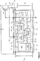
FIG. 1 is a schematic diagram, in overview, of a circuit comprising a power regulation apparatus constituting an embodiment of the invention; -
FIG. 2 is a schematic diagram of, inter alia, the power regulation apparatus ofFIG. 1 , the power regulation apparatus being shown in greater detail; -
FIG. 3 is a schematic diagram of the power regulation apparatus inFIG. 2 , but in further detail; -
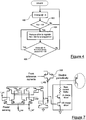
FIG. 4 is a flow diagram of the operation, in overview, of the apparatus ofFIG. 3 ; -
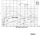
FIG. 5 is a graph of power dissipation curves and charging current curves in respect of three different voltage sources used at a first time; -
FIG. 6 is a graph of power dissipation curves and charge current curves for a single voltage source used, but at two different times; and -
FIG. 7 is a schematic diagram of part of the power regulation apparatus ofFIG. 3 . - Throughout the following description identical reference numerals will be used to identify like parts.
- Referring to
FIG. 1 , acharging arrangement 100 comprises anadapter 102 coupled to acharging system 104, thecharging system 104 being coupled to a cell, for example, abattery 106. Theadapter 102 can be represented as avoltage source 108 coupled in series to an equivalentinternal resistance 110 of theadapter 102, including the resistive contribution by an electrical plug (not shown) attached to theadapter 102. - The
charging system 104 is external to theadapter 102 and is disposed within an electronic device (not shown), for example a wireless communications device, such as a cellular telephone handset. The charging system has aninput terminal 112 coupled to anoutput terminal 114 of theadapter 102, for example by a two-core cable (not shown) and a pair of connectors (also not shown). The two-core cable has a positive voltage wire and a ground, or earth, wire. Theinput terminal 112 of thecharging system 104 comprises a positivepower supply rail 116 and aground rail 118, thepositive supply rail 116 being coupled to the positive voltage wire and theground rail 118 being coupled to the ground wire. In this example, the resistive losses of the cable are represented by aresistive loss 113. - The positive
power supply rail 116 is coupled to aninput 120 of acontroller 122, and afirst output terminal 124 of thecontroller 122 is coupled to theground rail 118. Asecond output terminal 126 of thecontroller 122 is coupled to aninput terminal 128 of a controlledcurrent source 130. - A
control terminal 132 of the drivecurrent source 130 is coupled to acontrol terminal 134 of apass device 136, asecond input terminal 138 of thepass device 136 being coupled to thepositive supply rail 116. Thepass device 136 is independent from theadapter 102. Anoutput terminal 140 of thepass device 136 is coupled directly to thecharging system 104 and also to afirst terminal 142 of an external, sensing,resistor 144, asecond terminal 146 of theexternal sensing resistor 144 also being coupled to thecharging system 104. The exact coupling between thepass device 136 and thecharging system 104 is described in greater later herein. Thepass device 136 is any suitable device capable of setting and modifying the flow of a charge current, Ich, to thebattery 106. In this example, thepass device 136 is a bipolar PNP transistor, but the skilled person will appreciate that other devices can be employed. - The
second terminal 146 of thesensing resistor 144 is also coupled to apositive voltage terminal 148 of thebattery 106, thebattery 106 being characterised as comprising an equivalentinternal resistance 150 of the battery coupled to at least onecell 152. Thepositive voltage terminal 148 of thebattery 106 is coupled to theinternal resistance 150, theinternal resistance 150, as explained above, being coupled to the at least onecell 152. The at least onecell 152 is coupled to aground terminal 154 of thebattery 106, theground terminal 154 of thebattery 106 being coupled theground rail 118 of thecharging system 104. - Turning to
FIG. 2 , thecontroller 122 comprises acontrol unit 200 having afirst terminal 202 thereof coupled to thepositive supply rail 116 and asecond terminal 204 thereof coupled to theground rail 118. Thecontrol unit 200 comprises acounter 206 having an output (not shown) coupled to anoutput terminal 208 of thecontrol unit 200. Theoutput terminal 208 of thecontrol unit 200 is coupled to afirst terminal 210 of apower sensing circuit 212. Asecond terminal 214 of thepower sensing circuit 212 is coupled to afirst terminal 216 of a differentialvoltage sensing circuit 218, asecond terminal 220 of the differentialvoltage sensing circuit 218 being coupled to thepositive supply rail 116. Athird terminal 222 of thepower sensing circuit 212 is also coupled to afirst terminal 224 of a chargecurrent sensing circuit 226, asecond terminal 228 of the chargecurrent sensing circuit 226 being coupled to athird terminal 230 of the differentialvoltage sensing circuit 218 and theoutput terminal 140 of thepass device 136. - A
third terminal 232 of the chargecurrent sensing circuit 226 is coupled to thesecond terminal 146 of thesensing resistor 144, and afourth terminal 234 of the chargecurrent sensing circuit 226 is coupled to agate terminal 236 of a first N-channel Metal Oxide Semiconductor (NMOS) Field Effect Transistor (FET) 238 of the drivecurrent source 130. Adrain terminal 240 of thefirst NMOS FET 238 is coupled to afirst terminal 242 of afirst load resistor 244, asecond terminal 246 of thefirst load resistor 244 being coupled to thefirst input terminal 134 of thepass device 136. Thefirst load resistor 244 provides additional protection to base of the PNP bipolar transistor that serves as thepass device 136. - A
source terminal 248 of thefirst NMOS FET 238 is coupled to adrain terminal 250 of asecond NMOS FET 252, asource terminal 254 of thesecond NMOS FET 252 being coupled to theground rail 118. Agate terminal 256 of thesecond NMOS FET 252 is coupled to afourth terminal 258 of thepower sensing circuit 212. - Referring to
FIG. 3 , thecontroller 122 comprises the differentialvoltage sensing circuit 218, the chargecurrent sensing circuit 226 and thepower sensing circuit 212. Although not shown inFIGs. 1 and2 , thecontroller 122 also comprises a referencecurrent generation circuit 300. - The differential
voltage sensing circuit 218 comprises an integratedsensing resistor R vce 302 coupled to thepositive power rail 116 and an inverting input terminal of a first operational amplifier 304 and a source terminal of a first P-channel Metal Oxide Semiconductor (PMOS)FET 306. A gate terminal of thefirst PMOS FET 306 is coupled to an output terminal of the operational amplifier 304. The non-inverting input terminal of the first operational amplifier 304 is coupled to theoutput terminal 140 of thepass device 136. The drain terminal of thefirst PMOS FET 306 is coupled to a current mirror arrangement 308. Together, theintegrated sensing resistor 302, the first operational amplifier 304, thefirst PMOS FET 306 and the current mirror arrangement 308 serve as a current source circuit for generating a first sensing current, Ivce, proportional to the collector-emitter voltage, Vce, of thepass device 136. - The non-inverting input terminal of the first operational amplifier 304 is also coupled to a
third sensing resistor 310, thethird sensing resistor 310 also being coupled to an inverting input terminal of a secondoperational amplifier 312 and a source terminal of asecond PMOS FET 314. A gate terminal of thesecond PMOS FET 314 is coupled to an output terminal of the secondoperational amplifier 312, and the drain terminal of thesecond PMOS FET 314 is coupled to a secondcurrent mirror arrangement 316. The secondcurrent mirror arrangement 316 is coupled to a thirdcurrent mirror arrangement 318. A non-inverting input terminal of the secondoperational amplifier 312 is coupled to thepositive voltage terminal 148 of thebattery 106. Together, thethird sensing resistor 310, thesecond PMOS FET 314, the secondoperational amplifier 312, and the second and thirdcurrent mirror arrangements pass device 136, i.e. the charging current, Ich, and is used to limit the charge current. - A
source terminal 320 of the thirdcurrent mirror arrangement 318 is coupled to a first terminal 322 of a Gilbert Cell arrangement 324. The Gilbert Cell arrangement 324 comprises a number of PMOS FETs and NPN bipolar transistors, the arrangement of which is known to the skilled person and so for the sake of conciseness will not be described further herein. - A
second terminal 326 of the Gilbert Cell arrangement 324 is coupled to a source of a reference voltage Vref (not shown). Athird terminal 328 of the Gilbert Cell arrangement 324 is coupled to adrain terminal 330 of the first current mirror arrangement 308, and afourth terminal 332 of the Gilbert Cell arrangement 324 is coupled to adrain terminal 334 of a fourthcurrent mirror arrangement 336 of the referencecurrent generation circuit 300. The Gilbert Cell arrangement 324 is coupled to a fifth current mirror arrangement 338, the fifth current mirror arrangement 338 being coupled to a sixthcurrent mirror arrangement 340. Adrain terminal 342 of the sixthcurrent mirror arrangement 340 provides a third sensing current, Ipw, that is proportional to a power dissipated, Pd, by thepass device 136. - The reference
current generation circuit 300 comprises a third operational amplifier 344 having a non-inverting input terminal coupled to the source of the reference voltage, Vref. Although not shown in the Figures, the circuit that generates the reference voltage, Vref, is a known standard feature of integrated circuits and routinely designed into the integrated circuits for use by a number of circuits making up the integrated circuit. Typically, the reference voltage, Vref, is a voltage that is stable with respect to temperature and manufacturing process variations. An array ofPMOS FETs 346 are coupled in parallel having their gate terminals coupled to an output terminal of the operational amplifier 344, an inverting input terminal and a drain terminal of afirst PMOS FET 348 of the array ofPMOS FETs 346 being coupled to theground rail 118 via areference resistor 350. A drain terminal of asecond PMOS FET 352 of the array ofPMOS FETs 346 is coupled to the fourthcurrent mirror arrangement 336. Together, the third operational amplifier 344, the array ofPMOS FETs 346, thereference resistor 350 and the fourthcurrent mirror arrangement 336 serve as a current source for generating reference currents, a first reference current, Iref, being provided at thedrain terminal 334 of the fourthcurrent mirror arrangement 336, a second, threshold reference charging, current, Irefc, being provided at a drain terminal of athird PMOS FET 354 of the array ofPMOS FETs 346, and a third, threshold power reference, current, Irefp, being provided at a drain terminal of afourth PMOS FET 356 of the array ofPMOS FETs 346. - In operation, the
adapter 102 is plugged into a power outlet as well as connected to the electronic device, thereby coupling theadapter 102 to thecharging system 104. Thebattery 106 is, of course, also coupled to thecharging system 104 in the manner already described above. - Upon powering up the
charging system 104, the reference voltage, Vref, is supplied to the referencecurrent generation circuit 300, causing the current source circuit therein to generate the first, second and third reference currents Iref, Irefc, Irefp. Thereference resistor 350 is set such that the threshold reference charging current, Irefc, corresponds to a predetermined maximum threshold current that is permitted to flow through thepass device 136 and thebattery 106 when the battery is being charged. In this example, the threshold reference charging current, Irefc, corresponds to a maximum charging current of 1A. Similarly, the setting of thereference resistor 350 also ensures that the threshold power reference current, Irefp, corresponds to a maximum permitted power dissipation by thepass device 136 of 1W. - At the same time, the current source of the differential
voltage sensing circuit 218 translates the voltage applied across thepositive power rail 116 and the non-inverting input terminal of the first operational amplifier 304 into the first sensing current Ivce. The voltage across thepositive power rail 116 and the non-inverting input terminal of the first operational amplifier 304, is the collector-emitter voltage, Vce, of thepass device 136 and so the second sensing current Ivce is proportional to the collector-emitter voltage, Vce, of thepass device 136. Additionally, a voltage across thefirst sensing resistor 144 is applied across the non-inverting input terminal of the first operational amplifier 304 and the non-inverting input terminal of the secondoperational amplifier 312. The voltage across thefirst sensing resistor 144 is translated by the current source circuit of the chargingcurrent sensing circuit 226 into the second sensing current, Icc. As already mentioned above, the second sensing current, Icc, is proportional to the current flowing though thepass device 136, corresponding to the charging current, Ich, of thecharging system 104. Thecharging system 104 therefore has a measure of the charging current, Ich, and the collector emitter voltage, Vce, of thepass device 136. - The Gilbert Cell arrangement 324, being a cross coupled differential amplifier, multiplies the value of the second sensing current, Icc, which is proportional to the charging current, Ich, by the first sensing current, Ivce, which is proportional to the collector-emitter voltage, Vce, to arrive at a power dissipated sensing current, Ipw, that is proportional to the power dissipated, Pd, by the
pass device 136. The reference voltage, Vref, serves to set a correct operating point for the Gilbert cell arrangement 324, and the first reference current, Iref, serves to provide a scaling factor for the third sensing current, Ipw, i.e. Ipw = (Ivce X Icc)/Iref. - Knowledge of the charge current, Ich, is used in combination with the threshold reference charge current, Irefc, to control the
first NMOS FET 238. In series with thefirst NMOS FET 238, thesecond NMOS FET 252 is controlled by the power dissipation sensing current, Ipw, in combination with the threshold power reference current, Irefp, thereby providing independent control of the current flowing through thepass device 136 and hence the charging current, Ich. - Turning to
FIGs. 4 and5 , in a first example of theadapter 102, thesupply rail 116 is at 8V, the resistance Rplug of theadapter 102 is 6Ω and the initial charge voltage across thebattery 106 is 3V. These initial parameters result in a first chargingcurrent curve 500 and a firstpower dissipation curve 502 for the power Pd dissipated by thepass device 136. In this first example, the threshold reference charge current, Irefc, and the second sensing current, Icc, flow in opposite directions resulting in a first error signal, Irefc-Icc, the first error signal serving as a control signal for thefirst NMOS FET 238 being amplified by the transconductance of thefirst NMOS FET 238 to act as a first control of a drive current for thepass device 136. Similarly, and referring toFIG. 7 , the threshold power reference current, Irefp, and the power dissipation sensing current, Ipw, flow in opposite directions resulting in a second error signal, Irefp-Ipw, the second error signal serving as a control signal for thesecond PMOS FET 252 being amplified by the transconductance of thesecond NMOS FET 252 to act as a second control of the drive current for thepass device 136. - Consequently, as the drive current increases, the power dissipated, Pd, by the
pass device 136 increases until it reaches afirst peak 504 of about 950mW. Thereafter, as the drive current is further increased, the power dissipated by thepass device 136 reduces to about 200mW. As a result, the first error signal does not reach a level (Step 400) sufficient to cause thefirst NMOS FET 238 to limit the drive current so as to limit the charging current flowing through thepass device 136 to the first predetermined threshold current of 1A. Similarly, the second error signal does not reach a level (Step 402) sufficient to cause thesecond NMOS FET 252 to limit the drive current so as to limit the power dissipated, Pd, by thepass device 136 to the second predetermined threshold power dissipation of 1W. - In a second example of the
adapter 102, thesupply rail 116 is at 10V, the resistance Rplug of theadapter 102 is 6Ω and the initial charge voltage across thebattery 106 is 3V. These initial parameters result in a second chargingcurrent curve 506 and a secondpower dissipation curve 508 for the power, Pd, dissipated by thepass device 136. However, as the current flowing through thepass device 136 increases to 1A, the first error signal begins to reach the level (Step 400) mentioned above that is sufficient to cause thefirst NMOS FET 238 to limit the drive current, thereby limiting the charging current, Ich, flowing through thepass device 136 to no more than the first predetermined threshold current of 1A. Since the power dissipated, Pd, by thepass device 136, when the first error signal dictates the charging current to be a maximum of 1A, is less than the predetermined threshold power dissipation of 1W, the second error signal does not reach the level (Step 402) sufficient to cause thesecond NMOS FET 252 to limit the drive current; the power dissipated, Pd, by thepass device 136, when 1A flows through thepass device 136, is about 700mW. - In a third example of the
adapter 102, thesupply rail 116 is at 12V, the resistance Rplug of theadapter 102 is 6Ω and the initial charge voltage across thebattery 106 is 3V. These initial parameters result in a third chargingcurrent curve 510 and a thirdpower dissipation curve 512 for the power, Pd, dissipated by thepass device 136. However, as the current flowing through thepass device 136 increases to 1A, the first error signal begins to reach the level (Step 400) mentioned above that is sufficient to cause thefirst NMOS FET 238 to limit the drive current, thereby limiting the charging current flowing through thepass device 136 to no more than the first predetermined threshold current of 1A. However, at the limited charging current of 1A, the power dissipated Pd by thepass device 136 is much higher than 1W (2.6W) and so the second error signal reaches the level (Step 402) sufficient to cause thesecond NMOS FET 252 to limit (Step 404) the PNP drive current to about 1mA and hence the charging current, Ich, to about 100mA, thereby reducing the power dissipated, Pd, by thepass device 136 to a maximum of 1W. Hence, it can be seen that the above described circuit limits the power dissipated, Pd, by thepass device 136 to a safe maximum value, in this example 1W. - The above examples related to initial parameters. However, as the charging of the
battery 106 progresses, the voltage across thebattery 106 rises. In a fourth example (FIG. 6 ) of theadapter 102, thesupply rail 116 is at 11V, the resistance Rplug of theadapter 102 is 6Ω and the initial charge voltage across thebattery 106 is 3V. These initial parameters result in a fourth chargingcurrent curve 600 and a fourthpower dissipation curve 602 for the power, Pd, dissipated by thepass device 136. However, as the current flowing through thepass device 136 increases to 1A, the first error signal begins to reach the level (Step 400) mentioned above that is sufficient to cause thefirst NMOS FET 238 to limit the drive current, thereby limiting the charging current flowing through thepass device 136 to no more than the first predetermined threshold current of 1A. At this point, the power being dissipated by thepass device 136 is 1.6W and so, when the first error signal dictates the charging current to be the maximum of 1A, the power dissipated, Pd, by thepass device 136 is higher than 1W (1.6W) and so the second error signal reaches the level (Step 402) sufficient to cause thesecond NMOS FET 252 to limit (Step 404) the PNP drive current to about 1mA and hence the charging current to about 100mA, thereby reducing the power dissipated, Pd, by thepass device 136 to a maximum of 1W. - As the charging of the
battery 106 progresses the voltage across thebattery 106 increases and hence the fourth chargingcurrent curve 600 and the fourthpower dissipation curve 602 change. Near the end of the charging cycle, a fifth chargingcurrent curve 604 and a fifth power dissipation curve 606 are respectively followed. In this respect, the first error signal would still causes thefirst NMOS FET 238 to limit (Step 400) the drive current to about 12.5mA and hence the charging current flowing through thepass device 136 to no more than 1A. However, the power dissipation characteristic of thepass device 136 shifts downwards, resulting in thepass device 136 dissipating less power when the charging current is 1A. Consequently, the second predetermined threshold power dissipation of 1W is no longer reached and the charging system has a refresh mechanism (Step 406) to ensure that the highest permissible charging current is flowing through thepass device 136 whilst maintaining the power dissipated, Pd, by the pass device to below the predetermined power dissipation threshold. - Therefore, in another embodiment, the
charging system 104, through the use of the first error signal ensures that the charging current flowing through thepass device 136 is at the predetermined threshold charging current (step 400). Then, using the second error signal, thecharging system 104 ensures that the power dissipated by thepass device 136 does not exceed (Step 402) the predetermined power dissipation threshold. Provided the predetermined power dissipation threshold is not exceeded, the charging current remains at the predetermined threshold charging current. However, as soon as the predetermined power dissipation threshold is exceeded, through use of the second error signal the second error signal causes the charging current to reduce (Step 404) to a value low enough to ensure the predetermined power dissipation threshold is no longer exceeded, whilst maintaining the charging current at as high a value as possible within the constraint of the predetermined power dissipation threshold. However, as mentioned above, as the charging cycle progresses the voltage across thebattery 106 increases and so the charging conditions change as well. Consequently, thecounter 206 of thecontroller 208 periodically disables (Step 406) thepower sensing circuit 212 for a predetermined temporary period of time, for example a disabling period of lOps every Is, but not so long so as to cause damage to thepass device 136 through excessive power dissipated by thepass device 136. When this happens, the drive current is controlled only by the first error signal and hence thecharging system 104 causes the charging current, Ich, flowing through thepass device 136 to return to the predetermined threshold charging current irrespective of the power dissipated, Pd, by thepass device 136. Subsequently, control by thepower sensing circuit 212 is reinstated after the predetermined temporary period of time and, through use of the second error signal, thepower sensing circuit 212 reduces the drive current to thepass device 136 to a safe level that is not more than the predetermined power dissipation threshold. Consequently, as the charging current and power dissipation characteristics of the pass device change during the charging cycle, the charging current is always maintained at a maximum possible value whilst the predetermined power dissipation threshold is not exceeded, thereby ensuring an optimum safe charge time. - Consequently, returning to the fifth power dissipation curve 606, whilst the first error signal limits the charging current flowing through the
pass device 136 to no more than 1 A, the second error signal does not reach a level sufficient to cause thesecond NMOS FET 252 to limit the drive current further; the drive current of about 12.5mA set by thefirst NMOS FET 238 therefore remains unchanged and the power dissipated, Pd, by thepass device 136 remains at the reduced level of 600mW. - Hence it can be seen that through controlling a first switching device coupled in series with a second switching device for charging current limitation, the first switching device can be used to provide additional control of the drive current controlling the pass device so as to ensure that the pass device does not dissipate power in excess of the predetermined threshold power dissipation level.
- Whilst in the above example, the
power sensing circuit 212 has been disabled, for example by a disabling PMOS FET 700 (FIG. 7 ), it will be apparent to the skilled person that any other suitable know technique for temporarily permitting the predetermined power dissipation threshold to be exceeded for the predetermined period of time can be employed. - It should be appreciated that although the above described example relates to the field of battery charging, the principles behind the above examples can be used in other applications, for example in relation to voltage regulator circuits, audio amplifier circuits, or any circuit that requires a pass device which may dissipate more power than it can withstand due to the supply of an unknown power source level to the pass device.
- It is thus possible to provide a control apparatus and a method of regulating power that performs real-time and accurate power dissipation calculations. The apparatus has a lower Bill Of Materials (BOM) cost, uses small and Low cost PNP transistor. Additionally, a low-cost unregulated adapter can be used with a charging system comprising the control apparatus. Further, the need for pass device temperature monitoring is no longer necessary. Also, the time taken to charge a battery is optimised and is maximised with respect to permissible power dissipation by the pass device. Another benefit is that the lifetime of the pass device is not curtailed through excessive power dissipation by the charge device.
Claims (11)
- A control apparatus (122) for controlling a pass device (136) coupled between an electrical power supply and a load, the apparatus comprising:an input for receiving power from the power supply;an output for supplying power to the load; anda current control circuit arranged to generate a first control signal for limiting, when in use, to a predetermined current level current flowing through the pass device (136); the apparatus characterised in that:
a power control circuit is arranged to generate a second control signal for controlling, when in use, power dissipated by the pass device (136) to a predetermined power dissipation level wherein the power control circuit is temporarily disableable for a predetermined period of time, in response to the power dissipated while the power control circuit is enabled being below the predetermined power dissipation level, wherein the predetermined period conforms to a predetermined frequency of occurrence. - An apparatus (122) as claimed in Claim 1, wherein the current control circuit generates the first control signal for driving, when in use, the pass device (136) in a linear regime thereof.
- An apparatus (122) as claimed in Claim 1 or Claim 2, wherein the power control circuit generates the second control signal for limiting current flowing through the pass device (136).
- An apparatus (122) as claimed in Claim 1 or Claim 2 or Claim 3, wherein the power control circuit generates the second control signal independently of the first control signal.
- An apparatus (122) as claimed in any one of the preceding claims, wherein the power control circuit is arranged, when in use, to permit temporarily the predetermined power dissipation level to be exceeded for a predetermined period of time.
- An apparatus (122) as claimed in Claim 5, wherein the predetermined power dissipation level is permitted to be exceeded at predetermined times.
- An apparatus (122) as claimed in Claim 1, wherein the power control circuit is arranged to be temporarily disabled at predetermined times.
- An apparatus (122) as claimed in any one of the preceding claims, wherein the load is a rechargeable cell.
- A method of regulating power in a circuit comprising a pass device (136) for coupling a power source to a load, the method comprising the steps of:measuring power dissipated by the pass device (136);controlling current flowing through the pass device (136), using a power control circuit, in response to the power circuit being enabled in response to the measured power dissipation so as to limit the power dissipation by the pass device (136) below a predetermined power dissipation level; andtemporarily disabling the power control circuit to allow the power dissipated to exceed the predetermined power dissipation level for a predetermined period of time in response to the measured power dissipation while the power control circuit is enabled being below the predetermined power dissipation level, wherein the predetermined period of time conforms to a predetermined frequency of occurrence.
- A method as claimed in Claim 9, further comprising the steps of:measuring current flowing through the pass device (136);controlling the current flowing through the pass device (136) in response to the measured current so as to limit the current flowing through the pass device to a predetermined current level.
- A method of charging a cell, comprising the steps of:coupling a power source to the load via a charging circuit; andregulating power in the circuit according to the method as claimed in Claim 9 or Claim 10.
Applications Claiming Priority (1)
| Application Number | Priority Date | Filing Date | Title |
|---|---|---|---|
| PCT/IB2005/000819 WO2006090203A1 (en) | 2005-02-22 | 2005-02-22 | Control apparatus and method of regulating power |
Publications (2)
| Publication Number | Publication Date |
|---|---|
| EP1856784A1 EP1856784A1 (en) | 2007-11-21 |
| EP1856784B1 true EP1856784B1 (en) | 2020-02-12 |
Family
ID=34964413
Family Applications (1)
| Application Number | Title | Priority Date | Filing Date |
|---|---|---|---|
| EP05708797.5A Expired - Lifetime EP1856784B1 (en) | 2005-02-22 | 2005-02-22 | Control apparatus and method of regulating power |
Country Status (5)
| Country | Link |
|---|---|
| US (1) | US8018200B2 (en) |
| EP (1) | EP1856784B1 (en) |
| CN (1) | CN100585980C (en) |
| TW (1) | TW200703843A (en) |
| WO (1) | WO2006090203A1 (en) |
Families Citing this family (13)
| Publication number | Priority date | Publication date | Assignee | Title |
|---|---|---|---|---|
| US7969275B2 (en) * | 2007-11-14 | 2011-06-28 | Enerdel, Inc. | Fuse assembly with integrated current sensing |
| CN101904081B (en) * | 2007-12-21 | 2013-10-09 | 桑迪士克科技股份有限公司 | Multi-regulator power delivery system for asic cores |
| US8294421B2 (en) * | 2008-09-05 | 2012-10-23 | O2Micro Inc | Cell balancing systems employing transformers |
| US8339108B2 (en) * | 2008-10-09 | 2012-12-25 | 02Micro Inc | Charging systems that control power dissipation in a charging path |
| JP5208149B2 (en) * | 2009-04-09 | 2013-06-12 | パナソニック株式会社 | Protection circuit and battery pack |
| US8084999B2 (en) * | 2009-06-02 | 2011-12-27 | Broadcom Corporation | Method for charging lithium batteries with power dissipation control |
| CN102570520A (en) * | 2010-12-22 | 2012-07-11 | 深圳富泰宏精密工业有限公司 | Charging circuit and charging method thereof |
| EP2846211A1 (en) | 2013-09-10 | 2015-03-11 | Dialog Semiconductor GmbH | Reduction in on-resistance in pass device |
| JP6104407B2 (en) | 2013-12-04 | 2017-03-29 | 三菱電機株式会社 | Semiconductor device |
| US20150263552A1 (en) * | 2014-03-12 | 2015-09-17 | Ergotron, Inc. | Electronic device charger |
| US10122259B2 (en) * | 2015-09-16 | 2018-11-06 | Semiconductor Components Industries, Llc | Over power protection for power converter |
| CN114167873B (en) * | 2021-12-09 | 2024-03-01 | 展讯通信(天津)有限公司 | Maze tracking robot and energy consumption adjusting method |
| CN114938136B (en) * | 2022-07-19 | 2022-11-01 | 伏达半导体(合肥)有限公司 | Power regulating device, double-battery charging device and charging current regulating method |
Family Cites Families (10)
| Publication number | Priority date | Publication date | Assignee | Title |
|---|---|---|---|---|
| US4937697A (en) * | 1989-05-22 | 1990-06-26 | Motorola, Inc. | Semiconductor device protection circuit |
| JP3620118B2 (en) * | 1995-10-24 | 2005-02-16 | 松下電器産業株式会社 | Constant current / constant voltage charger |
| US5764030A (en) * | 1997-03-14 | 1998-06-09 | International Components Corporation | Microcontrolled battery charger |
| US6144187A (en) * | 1998-11-12 | 2000-11-07 | Fairchild Semiconductor Corporation | Power measurement for adaptive battery charger |
| US6326769B1 (en) * | 2000-11-29 | 2001-12-04 | Telefonaktiebolaget Lm Ericsson (Publ) | Limitation of power dissipation in Li battery |
| US6522118B1 (en) | 2001-04-18 | 2003-02-18 | Linear Technology Corporation | Constant-current/constant-voltage current supply |
| US6498461B1 (en) * | 2001-08-17 | 2002-12-24 | O2 Micro International Limited | Voltage mode, high accuracy battery charger |
| US6667606B2 (en) * | 2002-02-15 | 2003-12-23 | Motorola, Inc. | Power regulation and thermal management circuit |
| US6771051B2 (en) * | 2002-06-29 | 2004-08-03 | Motorola, Inc. | Thermally limited battery protection and charging circuit |
| US6850040B2 (en) * | 2003-06-19 | 2005-02-01 | Motorola, Inc. | Charge boost battery charging and protection circuit |
-
2005
- 2005-02-22 CN CN200580048555A patent/CN100585980C/en not_active Expired - Fee Related
- 2005-02-22 WO PCT/IB2005/000819 patent/WO2006090203A1/en not_active Ceased
- 2005-02-22 US US11/816,040 patent/US8018200B2/en active Active
- 2005-02-22 EP EP05708797.5A patent/EP1856784B1/en not_active Expired - Lifetime
-
2006
- 2006-02-13 TW TW095104785A patent/TW200703843A/en unknown
Non-Patent Citations (1)
| Title |
|---|
| None * |
Also Published As
| Publication number | Publication date |
|---|---|
| TW200703843A (en) | 2007-01-16 |
| US20080094037A1 (en) | 2008-04-24 |
| CN101124708A (en) | 2008-02-13 |
| CN100585980C (en) | 2010-01-27 |
| US8018200B2 (en) | 2011-09-13 |
| WO2006090203A1 (en) | 2006-08-31 |
| EP1856784A1 (en) | 2007-11-21 |
Similar Documents
| Publication | Publication Date | Title |
|---|---|---|
| US11971734B2 (en) | Low dropout linear regulator and control circuit thereof | |
| US7656304B2 (en) | Method and apparatus for sensing a current in a circuit | |
| US9052728B2 (en) | Start-up circuit and method thereof | |
| US8242760B2 (en) | Constant-voltage circuit device | |
| US9231419B2 (en) | Semiconductor device and battery pack | |
| US6861824B1 (en) | Charger system with dual-level current regulation and dual-level thermal regulation | |
| US8018200B2 (en) | Control apparatus and method of regulating power | |
| CN101546920B (en) | Charge control circuit and charge controlling semiconductor integrated circuit | |
| JP2021518061A (en) | Low quiescent current load switch | |
| US7821233B2 (en) | Charging circuit | |
| CN101815974A (en) | Capacity-free low dropout voltage regulator with fast overvoltage response | |
| KR20130009599A (en) | Battery charging apparatus with a common control loop for a low drop-out voltage regulator and a boost regulator | |
| US8395359B2 (en) | Charge controller | |
| US8339108B2 (en) | Charging systems that control power dissipation in a charging path | |
| CN104571241B (en) | Voltage stabilizing circuit and method thereof | |
| JP4484839B2 (en) | Power supply control circuit and power supply control method | |
| JP6756754B2 (en) | Charge control device, charging system and charge control method | |
| US20140253019A1 (en) | Charger Circuit and Control Circuit and Control Method Thereof | |
| CN101345488A (en) | AC-DC Adapters for Mobile Systems | |
| CN111934404B (en) | charging circuit | |
| CN113572215A (en) | Controlled regulatory transitions | |
| JP2004515197A (en) | Charger circuit | |
| KR20070005881A (en) | A semiconductor device including a charging circuit and the charging circuit | |
| US9048661B2 (en) | Battery protection circuits | |
| CN119270968B (en) | Linear voltage regulators, chips and electronic devices |
Legal Events
| Date | Code | Title | Description |
|---|---|---|---|
| PUAI | Public reference made under article 153(3) epc to a published international application that has entered the european phase |
Free format text: ORIGINAL CODE: 0009012 |
|
| 17P | Request for examination filed |
Effective date: 20070924 |
|
| AK | Designated contracting states |
Kind code of ref document: A1 Designated state(s): AT BE BG CH CY CZ DE DK EE ES FI FR GB GR HU IE IS IT LI LT LU MC NL PL PT RO SE SI SK TR |
|
| DAX | Request for extension of the european patent (deleted) | ||
| RAP1 | Party data changed (applicant data changed or rights of an application transferred) |
Owner name: NXP USA, INC. |
|
| STAA | Information on the status of an ep patent application or granted ep patent |
Free format text: STATUS: EXAMINATION IS IN PROGRESS |
|
| 17Q | First examination report despatched |
Effective date: 20180725 |
|
| GRAP | Despatch of communication of intention to grant a patent |
Free format text: ORIGINAL CODE: EPIDOSNIGR1 |
|
| STAA | Information on the status of an ep patent application or granted ep patent |
Free format text: STATUS: GRANT OF PATENT IS INTENDED |
|
| INTG | Intention to grant announced |
Effective date: 20190628 |
|
| RIN1 | Information on inventor provided before grant (corrected) |
Inventor name: TICO, OLIVIER Inventor name: ENJALBERT, JEROME |
|
| GRAJ | Information related to disapproval of communication of intention to grant by the applicant or resumption of examination proceedings by the epo deleted |
Free format text: ORIGINAL CODE: EPIDOSDIGR1 |
|
| STAA | Information on the status of an ep patent application or granted ep patent |
Free format text: STATUS: EXAMINATION IS IN PROGRESS |
|
| INTC | Intention to grant announced (deleted) | ||
| GRAP | Despatch of communication of intention to grant a patent |
Free format text: ORIGINAL CODE: EPIDOSNIGR1 |
|
| STAA | Information on the status of an ep patent application or granted ep patent |
Free format text: STATUS: GRANT OF PATENT IS INTENDED |
|
| GRAS | Grant fee paid |
Free format text: ORIGINAL CODE: EPIDOSNIGR3 |
|
| GRAA | (expected) grant |
Free format text: ORIGINAL CODE: 0009210 |
|
| STAA | Information on the status of an ep patent application or granted ep patent |
Free format text: STATUS: THE PATENT HAS BEEN GRANTED |
|
| INTG | Intention to grant announced |
Effective date: 20191219 |
|
| REG | Reference to a national code |
Ref country code: DE Ref legal event code: R081 Ref document number: 602005056608 Country of ref document: DE Owner name: NXP USA, INC., AUSTIN, US Free format text: FORMER OWNER: FREESCALE SEMICONDUCTORS, INC., AUSTIN, TEX., US |
|
| AK | Designated contracting states |
Kind code of ref document: B1 Designated state(s): AT BE BG CH CY CZ DE DK EE ES FI FR GB GR HU IE IS IT LI LT LU MC NL PL PT RO SE SI SK TR |
|
| REG | Reference to a national code |
Ref country code: GB Ref legal event code: FG4D |
|
| REG | Reference to a national code |
Ref country code: CH Ref legal event code: EP |
|
| REG | Reference to a national code |
Ref country code: AT Ref legal event code: REF Ref document number: 1233372 Country of ref document: AT Kind code of ref document: T Effective date: 20200215 |
|
| REG | Reference to a national code |
Ref country code: IE Ref legal event code: FG4D |
|
| REG | Reference to a national code |
Ref country code: DE Ref legal event code: R096 Ref document number: 602005056608 Country of ref document: DE |
|
| PG25 | Lapsed in a contracting state [announced via postgrant information from national office to epo] |
Ref country code: FI Free format text: LAPSE BECAUSE OF FAILURE TO SUBMIT A TRANSLATION OF THE DESCRIPTION OR TO PAY THE FEE WITHIN THE PRESCRIBED TIME-LIMIT Effective date: 20200212 |
|
| REG | Reference to a national code |
Ref country code: LT Ref legal event code: MG4D |
|
| REG | Reference to a national code |
Ref country code: NL Ref legal event code: MP Effective date: 20200212 |
|
| PG25 | Lapsed in a contracting state [announced via postgrant information from national office to epo] |
Ref country code: SE Free format text: LAPSE BECAUSE OF FAILURE TO SUBMIT A TRANSLATION OF THE DESCRIPTION OR TO PAY THE FEE WITHIN THE PRESCRIBED TIME-LIMIT Effective date: 20200212 Ref country code: GR Free format text: LAPSE BECAUSE OF FAILURE TO SUBMIT A TRANSLATION OF THE DESCRIPTION OR TO PAY THE FEE WITHIN THE PRESCRIBED TIME-LIMIT Effective date: 20200513 Ref country code: IS Free format text: LAPSE BECAUSE OF FAILURE TO SUBMIT A TRANSLATION OF THE DESCRIPTION OR TO PAY THE FEE WITHIN THE PRESCRIBED TIME-LIMIT Effective date: 20200612 Ref country code: BG Free format text: LAPSE BECAUSE OF FAILURE TO SUBMIT A TRANSLATION OF THE DESCRIPTION OR TO PAY THE FEE WITHIN THE PRESCRIBED TIME-LIMIT Effective date: 20200512 |
|
| PG25 | Lapsed in a contracting state [announced via postgrant information from national office to epo] |
Ref country code: NL Free format text: LAPSE BECAUSE OF FAILURE TO SUBMIT A TRANSLATION OF THE DESCRIPTION OR TO PAY THE FEE WITHIN THE PRESCRIBED TIME-LIMIT Effective date: 20200212 |
|
| REG | Reference to a national code |
Ref country code: CH Ref legal event code: PL |
|
| REG | Reference to a national code |
Ref country code: BE Ref legal event code: MM Effective date: 20200229 |
|
| PG25 | Lapsed in a contracting state [announced via postgrant information from national office to epo] |
Ref country code: CZ Free format text: LAPSE BECAUSE OF FAILURE TO SUBMIT A TRANSLATION OF THE DESCRIPTION OR TO PAY THE FEE WITHIN THE PRESCRIBED TIME-LIMIT Effective date: 20200212 Ref country code: RO Free format text: LAPSE BECAUSE OF FAILURE TO SUBMIT A TRANSLATION OF THE DESCRIPTION OR TO PAY THE FEE WITHIN THE PRESCRIBED TIME-LIMIT Effective date: 20200212 Ref country code: SK Free format text: LAPSE BECAUSE OF FAILURE TO SUBMIT A TRANSLATION OF THE DESCRIPTION OR TO PAY THE FEE WITHIN THE PRESCRIBED TIME-LIMIT Effective date: 20200212 Ref country code: LT Free format text: LAPSE BECAUSE OF FAILURE TO SUBMIT A TRANSLATION OF THE DESCRIPTION OR TO PAY THE FEE WITHIN THE PRESCRIBED TIME-LIMIT Effective date: 20200212 Ref country code: ES Free format text: LAPSE BECAUSE OF FAILURE TO SUBMIT A TRANSLATION OF THE DESCRIPTION OR TO PAY THE FEE WITHIN THE PRESCRIBED TIME-LIMIT Effective date: 20200212 Ref country code: PT Free format text: LAPSE BECAUSE OF FAILURE TO SUBMIT A TRANSLATION OF THE DESCRIPTION OR TO PAY THE FEE WITHIN THE PRESCRIBED TIME-LIMIT Effective date: 20200705 Ref country code: DK Free format text: LAPSE BECAUSE OF FAILURE TO SUBMIT A TRANSLATION OF THE DESCRIPTION OR TO PAY THE FEE WITHIN THE PRESCRIBED TIME-LIMIT Effective date: 20200212 Ref country code: LU Free format text: LAPSE BECAUSE OF NON-PAYMENT OF DUE FEES Effective date: 20200222 Ref country code: EE Free format text: LAPSE BECAUSE OF FAILURE TO SUBMIT A TRANSLATION OF THE DESCRIPTION OR TO PAY THE FEE WITHIN THE PRESCRIBED TIME-LIMIT Effective date: 20200212 |
|
| REG | Reference to a national code |
Ref country code: DE Ref legal event code: R097 Ref document number: 602005056608 Country of ref document: DE |
|
| REG | Reference to a national code |
Ref country code: AT Ref legal event code: MK05 Ref document number: 1233372 Country of ref document: AT Kind code of ref document: T Effective date: 20200212 |
|
| PG25 | Lapsed in a contracting state [announced via postgrant information from national office to epo] |
Ref country code: CH Free format text: LAPSE BECAUSE OF NON-PAYMENT OF DUE FEES Effective date: 20200229 Ref country code: LI Free format text: LAPSE BECAUSE OF NON-PAYMENT OF DUE FEES Effective date: 20200229 Ref country code: MC Free format text: LAPSE BECAUSE OF FAILURE TO SUBMIT A TRANSLATION OF THE DESCRIPTION OR TO PAY THE FEE WITHIN THE PRESCRIBED TIME-LIMIT Effective date: 20200212 |
|
| PLBE | No opposition filed within time limit |
Free format text: ORIGINAL CODE: 0009261 |
|
| STAA | Information on the status of an ep patent application or granted ep patent |
Free format text: STATUS: NO OPPOSITION FILED WITHIN TIME LIMIT |
|
| 26N | No opposition filed |
Effective date: 20201113 |
|
| PG25 | Lapsed in a contracting state [announced via postgrant information from national office to epo] |
Ref country code: FR Free format text: LAPSE BECAUSE OF NON-PAYMENT OF DUE FEES Effective date: 20200412 Ref country code: AT Free format text: LAPSE BECAUSE OF FAILURE TO SUBMIT A TRANSLATION OF THE DESCRIPTION OR TO PAY THE FEE WITHIN THE PRESCRIBED TIME-LIMIT Effective date: 20200212 Ref country code: IT Free format text: LAPSE BECAUSE OF FAILURE TO SUBMIT A TRANSLATION OF THE DESCRIPTION OR TO PAY THE FEE WITHIN THE PRESCRIBED TIME-LIMIT Effective date: 20200212 Ref country code: IE Free format text: LAPSE BECAUSE OF NON-PAYMENT OF DUE FEES Effective date: 20200222 |
|
| PG25 | Lapsed in a contracting state [announced via postgrant information from national office to epo] |
Ref country code: PL Free format text: LAPSE BECAUSE OF FAILURE TO SUBMIT A TRANSLATION OF THE DESCRIPTION OR TO PAY THE FEE WITHIN THE PRESCRIBED TIME-LIMIT Effective date: 20200212 Ref country code: SI Free format text: LAPSE BECAUSE OF FAILURE TO SUBMIT A TRANSLATION OF THE DESCRIPTION OR TO PAY THE FEE WITHIN THE PRESCRIBED TIME-LIMIT Effective date: 20200212 Ref country code: BE Free format text: LAPSE BECAUSE OF NON-PAYMENT OF DUE FEES Effective date: 20200229 |
|
| PG25 | Lapsed in a contracting state [announced via postgrant information from national office to epo] |
Ref country code: TR Free format text: LAPSE BECAUSE OF FAILURE TO SUBMIT A TRANSLATION OF THE DESCRIPTION OR TO PAY THE FEE WITHIN THE PRESCRIBED TIME-LIMIT Effective date: 20200212 Ref country code: CY Free format text: LAPSE BECAUSE OF FAILURE TO SUBMIT A TRANSLATION OF THE DESCRIPTION OR TO PAY THE FEE WITHIN THE PRESCRIBED TIME-LIMIT Effective date: 20200212 |
|
| PGFP | Annual fee paid to national office [announced via postgrant information from national office to epo] |
Ref country code: GB Payment date: 20230121 Year of fee payment: 19 Ref country code: DE Payment date: 20230119 Year of fee payment: 19 |
|
| REG | Reference to a national code |
Ref country code: DE Ref legal event code: R119 Ref document number: 602005056608 Country of ref document: DE |
|
| GBPC | Gb: european patent ceased through non-payment of renewal fee |
Effective date: 20240222 |
|
| PG25 | Lapsed in a contracting state [announced via postgrant information from national office to epo] |
Ref country code: DE Free format text: LAPSE BECAUSE OF NON-PAYMENT OF DUE FEES Effective date: 20240903 |
|
| PG25 | Lapsed in a contracting state [announced via postgrant information from national office to epo] |
Ref country code: GB Free format text: LAPSE BECAUSE OF NON-PAYMENT OF DUE FEES Effective date: 20240222 |
|
| PG25 | Lapsed in a contracting state [announced via postgrant information from national office to epo] |
Ref country code: GB Free format text: LAPSE BECAUSE OF NON-PAYMENT OF DUE FEES Effective date: 20240222 Ref country code: DE Free format text: LAPSE BECAUSE OF NON-PAYMENT OF DUE FEES Effective date: 20240903 |