EP1855393A1 - Diversity receiver and gain adjusting method therefore - Google Patents
Diversity receiver and gain adjusting method therefore Download PDFInfo
- Publication number
- EP1855393A1 EP1855393A1 EP06714389A EP06714389A EP1855393A1 EP 1855393 A1 EP1855393 A1 EP 1855393A1 EP 06714389 A EP06714389 A EP 06714389A EP 06714389 A EP06714389 A EP 06714389A EP 1855393 A1 EP1855393 A1 EP 1855393A1
- Authority
- EP
- European Patent Office
- Prior art keywords
- reception level
- branches
- variable gain
- gain amplifiers
- branch
- Prior art date
- Legal status (The legal status is an assumption and is not a legal conclusion. Google has not performed a legal analysis and makes no representation as to the accuracy of the status listed.)
- Withdrawn
Links
Images


Classifications
-
- H—ELECTRICITY
- H04—ELECTRIC COMMUNICATION TECHNIQUE
- H04B—TRANSMISSION
- H04B7/00—Radio transmission systems, i.e. using radiation field
- H04B7/02—Diversity systems; Multi-antenna system, i.e. transmission or reception using multiple antennas
- H04B7/04—Diversity systems; Multi-antenna system, i.e. transmission or reception using multiple antennas using two or more spaced independent antennas
- H04B7/08—Diversity systems; Multi-antenna system, i.e. transmission or reception using multiple antennas using two or more spaced independent antennas at the receiving station
- H04B7/0837—Diversity systems; Multi-antenna system, i.e. transmission or reception using multiple antennas using two or more spaced independent antennas at the receiving station using pre-detection combining
- H04B7/0842—Weighted combining
- H04B7/0848—Joint weighting
- H04B7/0857—Joint weighting using maximum ratio combining techniques, e.g. signal-to- interference ratio [SIR], received signal strenght indication [RSS]
Definitions
- the present invention relates to a diversity receiver and a gain adjusting method therefor which are suitable for application to a W-CDMA (Wideband Code Division Multiple Access) based radio communication system.
- W-CDMA Wideband Code Division Multiple Access
- the receiver illustrated in Fig. 1 has a configuration which is predicated on a direct conversion scheme which directly converts a received radio frequency signal to a baseband signal.
- Direct conversion based receivers are described in detail, for example, in Japanese Patent No. 3329264 , Japanese Patent No. 3479835 , and the like.
- a signal received by antenna 1 is amplified by LNA (low-noise amplifier) 2.
- LNA low-noise amplifier
- the signal delivered from LNA 2 is converted to a baseband signal by orthogonal demodulator 4 after unwanted wave components which are the outside of a reception band have been removed by bandpass filter 3.
- bandpass filter 3 since the direct conversion scheme is assumed, local oscillator 5 generates a frequency which is the same as the carrier frequency of the received signal.
- Orthogonal demodulator 4 delivers two baseband signals, i.e., an I-signal which is a component in phase with a local signal, and a Q-signal which is a component orthogonal to the local signal.
- the I-signal and Q-signal are amplified by variable gain amplifiers (VGA) 6, 7, and converted to digital signals by A/D converters 10, 11 after unwanted wave components which are the outside of a using channel have been removed by low pass filters 8, 9.
- VGA variable gain amplifiers
- A/D converters 10, 11 used herein are of approximately eight bits taking into account the size of the circuit and operation speed. This results in approximately 50 dB of difference (dynamic range) between a maximal non-distortion input level available to A/D conversion and the quantization noise. Taking into consideration the peak factor of an input signal and the required S/N ratio, A/D converters 10, 11 cannot make use of their overall dynamic ranges. Therefore, the gains of variable gain amplifiers 6, 7 are adjusted such that the input levels to A/D converters 10, 11 present optimal values. Specifically, a target is set at a level approximately 10 dB lower than a maximal non-distortion input level which can be converted by A/D converters 10, 11 (called the "target level”) to adjust the gains of variable gain amplifiers 6, 7.
- I, Q in Equation (1) designate sample numbers of the digitally converted I-signal and Q-signal, and K designates a preceding number of the slot. Also, M designates the number of samples in the slot, and K+1 designates a sample number at the beginning point of the slot.
- the "slot" refers to a unit time for operational processing determined by the W-CDMA scheme. In the W-CDMA scheme, the average reception level is calculated on a slot-by-slot basis, and the gains of variable gain amplifiers 6, 7 are controlled based on that the value.
- Average reception level P calculated by reception level measuring unit 12 is supplied to gain setting circuit (Gain Setting) 13.
- Gain setting circuit (Gain Setting) 13 generates a control signal corresponding to the difference between average reception level P received from reception level measuring unit 12 and the target level to set the gains of variable gain amplifiers (VGA) 6, 7.
- VGA variable gain amplifiers
- Known configurations for variable gain amplifiers 6, 7 include changing the gains in response to an input voltage which is the control signal, or discretely controlling the gains in response to a digital signal which is the control signal, or the like. In this way, feedback control is conducted to optimize the input levels to A/D converters 10, 11.
- radio frequencies currently used by W-CDMA based radio communication systems are in a 2-GHz band, and the propagation characteristics deteriorates in rooms and the like, as compared with a 800-MHz band which is used by PDC (Personal Digital Cellular) and other radio communication systems. Accordingly, for purposes of compensating for deteriorated reception performance in a low electric-field range, studies have been made on the employment of a diversity reception scheme in the W-CDMA based radio communication system as well.
- Japanese Patent Laid-Open No. 2002-141844A describes a diversity receiver, for which the direct conversion scheme is not used, to measure the received power of each of two branches (receivers) by converting a radio frequency signal to an intermediate frequency signal and by detecting the envelope of the intermediate frequency signal.
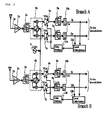
- Fig. 2 illustrates the configuration of a diversity reception scheme having two branches (receivers) A, B, given as an example, in which the circuit illustrated in Fig. 1 is applied, as is, to branch A and branch B. However, only local oscillator 5 is shared by branches A, B. While each component in Fig. 2 is designated a similar reference numeral to that in Fig. 1, a suffix "a” is added to reference numerals in branch A, and a suffix "b" is added in branch B for distinguishing them from each other.
- the gains of variable gain amplifiers are adjusted independently in each of branches A, B.
- An adjusting method therefor is completely similar to that used for the circuit illustrated in Fig. 1.
- branches A, B differ in average reception level, the gain of each variable gain amplifier is adjusted such that an input level to an A/D converter included in a branch to which the variable gain amplifier belongs is equal to the respective target level.
- Fig. 3 shows output levels of the variable gain amplifiers in the respective branches in the configuration illustrated in Fig. 2 after the gain adjustment.
- the vertical axis is in units of decibel (dB).
- branch A has a lower average reception level than branch B.
- the output level of each variable gain amplifier converges to the target level, as a result.
- branch B has an S/N ratio (Sb/Nb) of 30 dB.
- reception levels are measured in respective branches to compare the results of the measurements with one another to select the result of the measurement having a maximum reception level which is the highest reception level.
- the gains of variable gain amplifiers of all the branches including variable gain amplifiers belonging to a branch corresponding to the maximum reception level are adjusted to the same value such that output levels of the variable gain amplifiers are set to a preset target level.
- a diversity receiver and a gain adjusting method therefor of the present invention can restrain deterioration of the S/N ratio to produce effects resulting from the employment of the diversity reception scheme, as compared with the configuration illustrated in Fig. 2 which comprises two sets of circuits illustrated in Fig. 1 and which adjusts the gains independently on a branch-by-branch basis.
- circuit scale can be reduced because a feedback loop need not be included individually in each branch for gain adjustment.
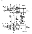
- Fig. 4 is a block diagram illustrating an exemplary configuration of a diversity receiver according to the present invention
- Fig. 5 is a graph showing the output level of each branch after a gain adjustment of the diversity receiver illustrated in Fig. 4.
- components similar to those in the conventional receiver illustrated in Fig. 2 are designated similar reference numerals to those in Fig. 2.
- the diversity receiver of the present invention is suitable for application to a radio communication system having a wide dynamic range of reception levels, like a W-CDMA scheme, which is required to finely adjust the gains of receivers, in order to carry out optimal and stable receptions.
- the receiver of this embodiment is a diversity receiver which comprises branches (Branches) A, B, and local oscillator 5 and gain setting circuit 13 shared by branches A, B.
- the diversity receiver of this embodiment differs in configuration from that illustrated in Fig. 2 in that it comprises level selector circuit (Level select) 14 for receiving average received power P of each of branches (Branches) A, B to select the highest average reception level P (maximum reception level) which is supplied to gain setting circuit (Gain Setting) 13.
- Level select level selector circuit
- the gains of branches A, B are adjusted respectively in accordance with the maximum reception level selected by this level selector circuit (Level select) 14.
- the adjustment is made based on the results of calculations by reception level measuring units 12a, 12b such that the input level of an A/D converter included in the branch presenting a higher average reception level is set to a target level.
- the branch presenting a lower average reception level is also set to the same gain as the branch presenting higher average reception level P in accordance with an output signal from gain setting circuit (Gain setting) 13.
- the difference in output signal level between the respective branches remains equal to the difference in level between signals received by the respective branches.
- the respective branches present substantially the same level because the signals pass through branch A and branch B in the same configuration with an equal gain.
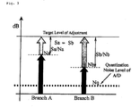
- the graph of Fig. 5 shows output levels of respective variable gain amplifiers 6a, 6b, 7a, 7b of branches A, B after gain adjustment in the configuration illustrated in Fig. 4.
- the vertical axis is in units of decibel (dB).
- branch A is lower than branch B in the received signal level.
- Level of branch A Branch B - 10 dB
- the gain is adjusted such that the output level of branch B is set to a target level, as shown in Fig. 5.
- noise power Na is equal to Nb.
- signal power Sa of branch A and signal power Sb of branch B are calculated by:
- total noise power N is twice as much as noise power Nb because there is no correlation between the branches, and is therefore calculated by:
- level selector circuit (Level select) 14 may receive average reception levels P of the respective branches calculated by a plurality of reception level measuring units (Level Calculation) to select and deliver the result of a measurement which presents the highest average reception level (maximum reception level) among them.
- gain setting circuit (Gain Setting) 13 sets all the variable gain amplifiers to the same gain based on the maximum reception level.
- the results of measurement of reception levels in respective branches are compared to select the result of a measurement indicative of a maximum reception level which is the highest reception level, and all variable gain amplifiers including variable gain amplifiers belonging to a branch corresponding to the maximum reception level are adjusted to the same gain such that the output levels of the variable gain amplifiers belonging to that branch are set to a preset target level. Consequently, deterioration in the S/N ratio is prevented, as compared with the configuration illustrated in Fig. 2 which comprises two sets of circuits illustrated in Fig. 1, and adjusts the gains independently on a branch-by-branch basis, thus producing the effect resulting from the employment of the diversity reception scheme.
- the circuit scale can be reduced because a feedback loop need not be included individually in each branch for gain adjustment.
- the gains of the variable gain amplifiers are also controlled based on the average received power value in each slot.
- the gain is constant within one slot, and the previous processing result (average received power) is reflected in the next slot to set all the variable gain amplifiers to the same gain based on the maximum reception level.
- a mobile terminal device comprising the diversity receiver of this embodiment comprises a storage element (slot)
- the processing result in the preceding slot can be utilized even if a communication is interrupted.
- a variety of controls including the gain adjustment can be conducted with reference to the processing result in the preceding slot in a waiting state (intermittent reception) or when no packet is available.
- circuits such as a combiner circuit and a demodulator circuit (not shown) disposed at stages subsequent to A/D converters 10a, 10b, 11a, 11 b, reception level measuring unit 12, level selector circuit 14 and the like can be contained in a single integrated circuit device.
- the integrated circuit is only required to deliver three signals, i.e., strobe, data, and clock to the outside (gain setting circuit 13).
Landscapes
- Engineering & Computer Science (AREA)
- Computer Networks & Wireless Communication (AREA)
- Signal Processing (AREA)
- Radio Transmission System (AREA)
Abstract
Description
- The present invention relates to a diversity receiver and a gain adjusting method therefor which are suitable for application to a W-CDMA (Wideband Code Division Multiple Access) based radio communication system.
- Referring to Fig. 1, a description will be first given of the configuration of a conventional receiver, used in a W-CDMA based radio communication system, which does not employ a diversity reception scheme. It should be noted that the receiver illustrated in Fig. 1 has a configuration which is predicated on a direct conversion scheme which directly converts a received radio frequency signal to a baseband signal. Direct conversion based receivers are described in detail, for example, in
Japanese Patent No. 3329264 Japanese Patent No. 3479835 - As illustrated in Fig. 1, in the conventional receiver, a signal received by antenna 1 is amplified by LNA (low-noise amplifier) 2. The signal delivered from LNA 2 is converted to a baseband signal by orthogonal demodulator 4 after unwanted wave components which are the outside of a reception band have been removed by bandpass filter 3. Here, since the direct conversion scheme is assumed, local oscillator 5 generates a frequency which is the same as the carrier frequency of the received signal.
- Orthogonal demodulator 4 delivers two baseband signals, i.e., an I-signal which is a component in phase with a local signal, and a Q-signal which is a component orthogonal to the local signal. The I-signal and Q-signal are amplified by variable gain amplifiers (VGA) 6, 7, and converted to digital signals by A/
D converters 10, 11 after unwanted wave components which are the outside of a using channel have been removed by low pass filters 8, 9. - Generally, A/
D converters 10, 11 used herein are of approximately eight bits taking into account the size of the circuit and operation speed. This results in approximately 50 dB of difference (dynamic range) between a maximal non-distortion input level available to A/D conversion and the quantization noise. Taking into consideration the peak factor of an input signal and the required S/N ratio, A/D converters 10, 11 cannot make use of their overall dynamic ranges. Therefore, the gains of variable gain amplifiers 6, 7 are adjusted such that the input levels to A/D converters 10, 11 present optimal values. Specifically, a target is set at a level approximately 10 dB lower than a maximal non-distortion input level which can be converted by A/D converters 10, 11 (called the "target level") to adjust the gains of variable gain amplifiers 6, 7. - The I-signal and Q-signal delivered from A/
D converters 10, 11, after they have been converted to digital signals, are supplied to a demodulator circuit (Demodulator), not shown, to restore the original signal. Also, the I-signal and Q-signal delivered from A/D converters 10, 11 are supplied to reception level measuring unit (Level Calculation) 12 to calculate average reception level (power) P for each slot in accordance with the following Equation (1): -

- Average reception level P calculated by reception level measuring unit 12 is supplied to gain setting circuit (Gain Setting) 13. Gain setting circuit (Gain Setting) 13 generates a control signal corresponding to the difference between average reception level P received from reception level measuring unit 12 and the target level to set the gains of variable gain amplifiers (VGA) 6, 7. Known configurations for variable gain amplifiers 6, 7 include changing the gains in response to an input voltage which is the control signal, or discretely controlling the gains in response to a digital signal which is the control signal, or the like. In this way, feedback control is conducted to optimize the input levels to A/
D converters 10, 11. - The foregoing description has been given of the configuration of the conventional receiver, used in a W-CDMA based radio communication system and the like, which does not employ a diversity reception scheme.
- Incidentally, radio frequencies currently used by W-CDMA based radio communication systems are in a 2-GHz band, and the propagation characteristics deteriorates in rooms and the like, as compared with a 800-MHz band which is used by PDC (Personal Digital Cellular) and other radio communication systems. Accordingly, for purposes of compensating for deteriorated reception performance in a low electric-field range, studies have been made on the employment of a diversity reception scheme in the W-CDMA based radio communication system as well.
- In regard to a general diversity receiver, which is not based on use with a W-CDMA scheme, an exemplary configuration thereof is described, for example, in
Japanese Patent Laid-Open No. 2002-141844A Japanese Patent Laid-Open No. 2002-141844A - When the diversity reception scheme is applied to the W-CDMA based radio communication system, problems as described below will arise if a diversity reception based receiver is designed as illustrated in Fig. 2 by simply using the conventional receiver illustrated in Fig. 1.
- Fig. 2 illustrates the configuration of a diversity reception scheme having two branches (receivers) A, B, given as an example, in which the circuit illustrated in Fig. 1 is applied, as is, to branch A and branch B. However, only local oscillator 5 is shared by branches A, B. While each component in Fig. 2 is designated a similar reference numeral to that in Fig. 1, a suffix "a" is added to reference numerals in branch A, and a suffix "b" is added in branch B for distinguishing them from each other.
- In such a configuration, the gains of variable gain amplifiers are adjusted independently in each of branches A, B. An adjusting method therefor is completely similar to that used for the circuit illustrated in Fig. 1. However, since branches A, B differ in average reception level, the gain of each variable gain amplifier is adjusted such that an input level to an A/D converter included in a branch to which the variable gain amplifier belongs is equal to the respective target level.
- Fig. 3 shows output levels of the variable gain amplifiers in the respective branches in the configuration illustrated in Fig. 2 after the gain adjustment. In the graph of Fig. 3, the vertical axis is in units of decibel (dB). Also, assume herein that branch A has a lower average reception level than branch B. In such an event, since the gains of the variable gain amplifiers are adjusted independently in each of the branches as described above, the output level of each variable gain amplifier converges to the target level, as a result.
- Assume herein that branch B has an S/N ratio (Sb/Nb) of 30 dB. Specifically,
-


-

- As output signals from these two branches are combined in a circuit at a subsequent stage, not shown, the respective signals are added in phase with each other, so that total signal power S is calculated by:
-

-

-
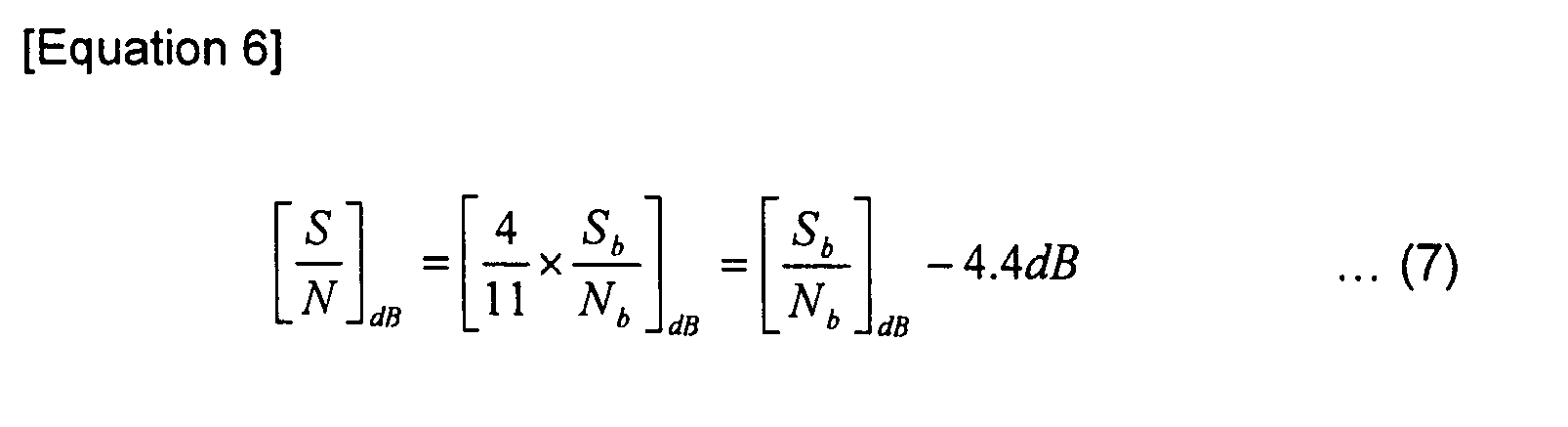
- In this way, when two sets of circuits illustrated in Fig. 1 are provided, and the gains are adjusted independently on a branch-by-branch basis, the S/N ratio is lower than the ratio that results from a reception signal by only one branch output which presents a higher average reception signal. Another disadvantage is that the number of feedback loops for adjusting the gains is the same as number of branches which results in a complicated circuit configuration.
- Accordingly, it is an object of the present invention to provide a diversity receiver which is capable of reducing deterioration in the S/N ratio in a simple circuit configuration, and to provide a gain adjusting method therefor.
- To achieve the above object, in the present invention, reception levels are measured in respective branches to compare the results of the measurements with one another to select the result of the measurement having a maximum reception level which is the highest reception level. The gains of variable gain amplifiers of all the branches including variable gain amplifiers belonging to a branch corresponding to the maximum reception level are adjusted to the same value such that output levels of the variable gain amplifiers are set to a preset target level.
- Thus, a diversity receiver and a gain adjusting method therefor of the present invention can restrain deterioration of the S/N ratio to produce effects resulting from the employment of the diversity reception scheme, as compared with the configuration illustrated in Fig. 2 which comprises two sets of circuits illustrated in Fig. 1 and which adjusts the gains independently on a branch-by-branch basis.
- In addition, the circuit scale can be reduced because a feedback loop need not be included individually in each branch for gain adjustment.
-
- [Fig. 1]
Fig. 1 is a block diagram illustrating the configuration of a conventional receiver which does not employ a diversity reception scheme. - [Fig. 2]
Fig. 2 is a block diagram illustrating an exemplary configuration of a diversity receiver which employs the receiver illustrated in Fig. 1 in each branch. - [Fig. 3]
Fig. 3 is a graph showing an output level of each branch after a gain adjustment of the diversity receiver illustrated in Fig. 2. - [Fig. 4]
Fig. 4 is a block diagram illustrating an exemplary configuration of a diversity receiver according to the present invention. - [Fig. 5]
Fig. 5 is a graph showing an output level of each branch after a gain adjustment of the diversity receiver illustrated in Fig. 4. - Fig. 4 is a block diagram illustrating an exemplary configuration of a diversity receiver according to the present invention, and Fig. 5 is a graph showing the output level of each branch after a gain adjustment of the diversity receiver illustrated in Fig. 4. In Fig. 4, components similar to those in the conventional receiver illustrated in Fig. 2 are designated similar reference numerals to those in Fig. 2.
- The diversity receiver of the present invention is suitable for application to a radio communication system having a wide dynamic range of reception levels, like a W-CDMA scheme, which is required to finely adjust the gains of receivers, in order to carry out optimal and stable receptions.
- As illustrated in Fig. 4, the receiver of this embodiment is a diversity receiver which comprises branches (Branches) A, B, and local oscillator 5 and gain setting
circuit 13 shared by branches A, B. - The diversity receiver of this embodiment differs in configuration from that illustrated in Fig. 2 in that it comprises level selector circuit (Level select) 14 for receiving average received power P of each of branches (Branches) A, B to select the highest average reception level P (maximum reception level) which is supplied to gain setting circuit (Gain Setting) 13. In the diversity receiver of this embodiment, the gains of branches A, B are adjusted respectively in accordance with the maximum reception level selected by this level selector circuit (Level select) 14.
- More specifically, the adjustment is made based on the results of calculations by reception
level measuring units - Accordingly, in the configuration of this embodiment, the difference in output signal level between the respective branches remains equal to the difference in level between signals received by the respective branches. In regard to the noise level, on the other hand, the respective branches present substantially the same level because the signals pass through branch A and branch B in the same configuration with an equal gain.
- The graph of Fig. 5 shows output levels of respective
variable gain amplifiers - Assume herein that branch A is lower than branch B in the received signal level.
- Specifically, assume that:
S/N Ratio of Branch B: Sb/Nb = 30 dB,
Level of branch A: Branch B - 10 dB, and
S/N Ratio of Branch A: Sa/Na = Sb/Nb - 10 dB = 20 dB - In this embodiment, the gain is adjusted such that the output level of branch B is set to a target level, as shown in Fig. 5.
- In this event, since branches A, B are identical in gain and circuit configuration, noise power Na is equal to Nb.
-

-

-

-

-

-

- While the diversity receiver of the present invention has been described above by giving, as an example, a configuration which comprises two branches (receivers), the number of branches is not limited to two, but may be equal to or larger than that. In this event, level selector circuit (Level select) 14 may receive average reception levels P of the respective branches calculated by a plurality of reception level measuring units (Level Calculation) to select and deliver the result of a measurement which presents the highest average reception level (maximum reception level) among them. In this event, gain setting circuit (Gain Setting) 13 sets all the variable gain amplifiers to the same gain based on the maximum reception level.
- According to the diversity receiver of this embodiment, the results of measurement of reception levels in respective branches are compared to select the result of a measurement indicative of a maximum reception level which is the highest reception level, and all variable gain amplifiers including variable gain amplifiers belonging to a branch corresponding to the maximum reception level are adjusted to the same gain such that the output levels of the variable gain amplifiers belonging to that branch are set to a preset target level. Consequently, deterioration in the S/N ratio is prevented, as compared with the configuration illustrated in Fig. 2 which comprises two sets of circuits illustrated in Fig. 1, and adjusts the gains independently on a branch-by-branch basis, thus producing the effect resulting from the employment of the diversity reception scheme. In addition, the circuit scale can be reduced because a feedback loop need not be included individually in each branch for gain adjustment.
- In the W-CDMA based radio communication system, signal processing is performed on a slot-by-slot basis as described above. Accordingly, the gains of the variable gain amplifiers are also controlled based on the average received power value in each slot. Here, the gain is constant within one slot, and the previous processing result (average received power) is reflected in the next slot to set all the variable gain amplifiers to the same gain based on the maximum reception level. In other words, since a mobile terminal device comprising the diversity receiver of this embodiment comprises a storage element (slot), the processing result in the preceding slot can be utilized even if a communication is interrupted. For example, a variety of controls including the gain adjustment can be conducted with reference to the processing result in the preceding slot in a waiting state (intermittent reception) or when no packet is available.
- In the configuration illustrated in Fig. 4, circuits such as a combiner circuit and a demodulator circuit (not shown) disposed at stages subsequent to A/
D converters level selector circuit 14 and the like can be contained in a single integrated circuit device. In this event, the integrated circuit is only required to deliver three signals, i.e., strobe, data, and clock to the outside (gain setting circuit 13). - On the other hand, in the configuration illustrated in Fig. 2, twice as many signals are delivered from an integrated circuit device to the outside (gain setting circuit 13). Recent mobile terminal devices experience significant difficulties as regards increasing the size of the mounting area. If the use of the diversity reception scheme results in a receiver having an increased number of components and consequently causes an increased in the number of terminals in the integrated circuit device which will require a larger mounting area, the integrated circuit device cannot be potentially mounted in the mobile terminal device. Thus, a reduction in circuit scale, as in the present invention, produces significant effects, if an increase in the number of terminals can be limited even to three.
Claims (5)
- A diversity receiver including a plurality of branches each comprised of a direct conversion type receiver, said diversity receiver comprising:a plurality of variable gain amplifiers, the gains of which can be controlled, for amplifying a received signal of each of said branches;a plurality of reception level measuring circuits for measuring a reception level in each of said branches to deliver the result of the measurement;a reception level selector circuit for comparing the results of the measurements of the reception levels in the respective branches to select and deliver the result of the measurement of a maximum reception level which is the highest reception level; anda gain setting circuit for adjusting the variable gain amplifiers of all branches, including variable gain amplifiers belonging to a branch corresponding to the maximum reception level, to the same gain such that output levels of said variable gain amplifiers are set to a preset predetermined value.
- The diversity receiver according to claim 1, wherein:said reception level measuring circuit calculates average power of the reception levels on a slot-by-slot basis, said slot indicating a preset predetermined time interval, to deliver the calculated average power as the result of the measurement of the reception level, andsaid reception level selector circuit determines the maximum reception level for each of the slots, and sets all the variable gain amplifiers to the same gain based on the maximum reception level.
- The diversity receiver according to claim 1 or 2, wherein said reception level measuring circuit and said reception level selector circuit are included in a single integrated circuit device.
- A gain adjusting method for a diversity receiver which comprises a plurality of branches each including a direct conversion type receiver, said each branch comprising a plurality of variable gain amplifiers, the gains of which can be controlled, said method comprising:measuring a reception level for each of said branches to deliver the respective results of the measurements;comparing the measurement results of reception levels in said respective branches with one another to select the result of the measurement of a maximum reception level which is the highest reception level; andadjusting the variable gain amplifiers of all said branches, including variable gain amplifiers belonging to a branch corresponding to the maximum reception level, to the same gain such that output levels of said variable gain amplifiers are set to a preset predetermined value.
- The gain adjusting method for a diversity receiver according to claim 4, comprising:calculating average power of the reception levels for each slot which is a preset time interval, as the result of the measurement of the reception level; anddetermining the maximum reception level for each said slot, and setting all the variable gain amplifiers to the same gain based on the maximum reception level.
Applications Claiming Priority (2)
| Application Number | Priority Date | Filing Date | Title |
|---|---|---|---|
| JP2005057480 | 2005-03-02 | ||
| PCT/JP2006/303249 WO2006093012A1 (en) | 2005-03-02 | 2006-02-23 | Diversity receiver and gain adjusting method therefore |
Publications (2)
| Publication Number | Publication Date |
|---|---|
| EP1855393A1 true EP1855393A1 (en) | 2007-11-14 |
| EP1855393A4 EP1855393A4 (en) | 2012-05-09 |
Family
ID=36941046
Family Applications (1)
| Application Number | Title | Priority Date | Filing Date |
|---|---|---|---|
| EP06714389A Withdrawn EP1855393A4 (en) | 2005-03-02 | 2006-02-23 | Diversity receiver and gain adjusting method therefore |
Country Status (5)
| Country | Link |
|---|---|
| US (1) | US7856216B2 (en) |
| EP (1) | EP1855393A4 (en) |
| JP (1) | JP4706871B2 (en) |
| CN (1) | CN101133567A (en) |
| WO (1) | WO2006093012A1 (en) |
Cited By (6)
| Publication number | Priority date | Publication date | Assignee | Title |
|---|---|---|---|---|
| US8054922B2 (en) | 2007-12-21 | 2011-11-08 | Mediatek Inc. | Parameter estimation for modulated signals |
| US8149702B2 (en) | 2007-12-21 | 2012-04-03 | Mediatek Inc. | Multi-mode bit rate processor |
| US8155241B2 (en) | 2007-12-21 | 2012-04-10 | Mediatek Inc. | System for processing common gain values |
| US8316378B2 (en) | 2007-12-21 | 2012-11-20 | Mediatek Inc. | Data flow control in wireless communication systems |
| CN101465837B (en) * | 2007-12-21 | 2013-02-27 | 联发科技股份有限公司 | Method and system for processing common gain values |
| US8488662B2 (en) | 2007-12-21 | 2013-07-16 | Mediatek Inc. | Receiver bit rate processing |
Families Citing this family (4)
| Publication number | Priority date | Publication date | Assignee | Title |
|---|---|---|---|---|
| JP4816949B2 (en) * | 2006-11-08 | 2011-11-16 | 日本電気株式会社 | CDMA receiver, profile synthesis path search method and program |
| KR101454027B1 (en) * | 2007-08-10 | 2014-10-24 | 한국전자통신연구원 | Time Division Multiplexing Communication System and Method Having Parallel Structure |
| JP2009060178A (en) * | 2007-08-29 | 2009-03-19 | Sharp Corp | Diversity device |
| WO2014049005A1 (en) * | 2012-09-25 | 2014-04-03 | Telefonaktiebolaget L M Ericsson (Publ) | A receiver arrangement and a method therein |
Family Cites Families (9)
| Publication number | Priority date | Publication date | Assignee | Title |
|---|---|---|---|---|
| US3364428A (en) * | 1964-06-09 | 1968-01-16 | Leonard R Kahn | Diversity receiver system with sequential comparison and control of signal segments in amplitude and phase |
| US3528012A (en) * | 1967-02-13 | 1970-09-08 | Kahn Res Lab | Phase control circuitry for placing diversely received signals in phase coincidence |
| JP3126426B2 (en) * | 1990-07-27 | 2001-01-22 | 株式会社東芝 | Automatic power control device and wireless communication device having automatic power control function |
| JPH09247005A (en) * | 1996-03-07 | 1997-09-19 | Fujitsu Ltd | Adaptive array receiver |
| JP2001168780A (en) | 1999-12-08 | 2001-06-22 | Sharp Corp | Diversity receiver |
| JP4357732B2 (en) | 2000-11-02 | 2009-11-04 | パナソニック株式会社 | Diversity receiver |
| JP4744725B2 (en) * | 2001-05-25 | 2011-08-10 | 三菱電機株式会社 | Interference canceller |
| WO2004095731A1 (en) * | 2003-04-21 | 2004-11-04 | Sanyo Electric Co., Ltd. | Reception device |
| JP2005006252A (en) * | 2003-06-16 | 2005-01-06 | Oki Electric Ind Co Ltd | Transmission power control method and system |
-
2006
- 2006-02-23 JP JP2007505872A patent/JP4706871B2/en not_active Expired - Fee Related
- 2006-02-23 EP EP06714389A patent/EP1855393A4/en not_active Withdrawn
- 2006-02-23 US US11/817,110 patent/US7856216B2/en not_active Expired - Fee Related
- 2006-02-23 CN CN200680007012.0A patent/CN101133567A/en active Pending
- 2006-02-23 WO PCT/JP2006/303249 patent/WO2006093012A1/en not_active Ceased
Cited By (6)
| Publication number | Priority date | Publication date | Assignee | Title |
|---|---|---|---|---|
| US8054922B2 (en) | 2007-12-21 | 2011-11-08 | Mediatek Inc. | Parameter estimation for modulated signals |
| US8149702B2 (en) | 2007-12-21 | 2012-04-03 | Mediatek Inc. | Multi-mode bit rate processor |
| US8155241B2 (en) | 2007-12-21 | 2012-04-10 | Mediatek Inc. | System for processing common gain values |
| US8316378B2 (en) | 2007-12-21 | 2012-11-20 | Mediatek Inc. | Data flow control in wireless communication systems |
| CN101465837B (en) * | 2007-12-21 | 2013-02-27 | 联发科技股份有限公司 | Method and system for processing common gain values |
| US8488662B2 (en) | 2007-12-21 | 2013-07-16 | Mediatek Inc. | Receiver bit rate processing |
Also Published As
| Publication number | Publication date |
|---|---|
| WO2006093012A1 (en) | 2006-09-08 |
| EP1855393A4 (en) | 2012-05-09 |
| JPWO2006093012A1 (en) | 2008-08-07 |
| JP4706871B2 (en) | 2011-06-22 |
| US7856216B2 (en) | 2010-12-21 |
| CN101133567A (en) | 2008-02-27 |
| US20090011731A1 (en) | 2009-01-08 |
Similar Documents
| Publication | Publication Date | Title |
|---|---|---|
| EP1655848B1 (en) | Method and apparatus for continuously controlling the dynamic range of an analog-to-digital converter | |
| KR100221163B1 (en) | Apparatus and method for optimizing the quality of a received signal in a radio receiver | |
| US7072632B2 (en) | Fast signal detection process | |
| US6614806B1 (en) | Method and apparatus for interfering receiver signal overload protection | |
| CN101449486A (en) | Automatic Gain Control for Frequency Hopping OFDM | |
| EP1654814A2 (en) | Radio transmitter with accurate power control | |
| JP4610697B2 (en) | Transmission power control method and wireless communication apparatus | |
| US6775336B1 (en) | Receiver and gain control method of the same | |
| US7856216B2 (en) | Diversity receiver and gain adjusting method therefor | |
| US7110735B2 (en) | Automatic gain control system | |
| WO2005011165A1 (en) | Radio receiver and automatic gain control method | |
| US7054605B1 (en) | Variable-gain low noise amplifier to reduce linearity requirements on a radio receiver | |
| US20080160945A1 (en) | Automatic gain controller for rf transceiver | |
| EP2151062B1 (en) | Increasing sensitivity of radio receiver | |
| US6404757B1 (en) | Reception method and apparatus in CDMA system | |
| CN116017666A (en) | AGC implementation method, device and system based on multi-level output signal strength detection | |
| JP2001339455A (en) | Receiving device and wireless communication device | |
| JP2000165272A (en) | Wireless base station equipment | |
| JP2009177568A (en) | Receiving device and electronic device using the same | |
| EP1306977A2 (en) | Receiver circuit for use in radio communications and communications unit including such a circuit | |
| JP2008053895A (en) | Radio receiver and gain control method thereof | |
| JPH11163782A (en) | Wireless base station device | |
| KR20010026355A (en) | Apparatus and method for sampling received signal for power control in mobile telecommunication system | |
| JP2001345782A (en) | Receiver | |
| JP2007150949A (en) | Receiving machine |
Legal Events
| Date | Code | Title | Description |
|---|---|---|---|
| PUAI | Public reference made under article 153(3) epc to a published international application that has entered the european phase |
Free format text: ORIGINAL CODE: 0009012 |
|
| 17P | Request for examination filed |
Effective date: 20070830 |
|
| AK | Designated contracting states |
Kind code of ref document: A1 Designated state(s): DE FR GB IT |
|
| RBV | Designated contracting states (corrected) |
Designated state(s): DE FR GB IT |
|
| DAX | Request for extension of the european patent (deleted) | ||
| A4 | Supplementary search report drawn up and despatched |
Effective date: 20120405 |
|
| RIC1 | Information provided on ipc code assigned before grant |
Ipc: H04B 7/08 20060101AFI20120330BHEP |
|
| RAP1 | Party data changed (applicant data changed or rights of an application transferred) |
Owner name: WARREN & LEWIS INVESTMENT CORPORATION |
|
| STAA | Information on the status of an ep patent application or granted ep patent |
Free format text: STATUS: THE APPLICATION IS DEEMED TO BE WITHDRAWN |
|
| 18D | Application deemed to be withdrawn |
Effective date: 20140902 |