EP1854697A1 - Electric assembly for monitoring the dynamic of a micro controller with a relay interface - Google Patents
Electric assembly for monitoring the dynamic of a micro controller with a relay interface Download PDFInfo
- Publication number
- EP1854697A1 EP1854697A1 EP06290777A EP06290777A EP1854697A1 EP 1854697 A1 EP1854697 A1 EP 1854697A1 EP 06290777 A EP06290777 A EP 06290777A EP 06290777 A EP06290777 A EP 06290777A EP 1854697 A1 EP1854697 A1 EP 1854697A1
- Authority
- EP
- European Patent Office
- Prior art keywords
- output
- input
- contact
- voltage
- working
- Prior art date
- Legal status (The legal status is an assumption and is not a legal conclusion. Google has not performed a legal analysis and makes no representation as to the accuracy of the status listed.)
- Granted
Links
- 238000012544 monitoring process Methods 0.000 title claims abstract description 35
- 238000005259 measurement Methods 0.000 claims abstract description 11
- 230000003321 amplification Effects 0.000 claims description 22
- 238000003199 nucleic acid amplification method Methods 0.000 claims description 22
- 239000003990 capacitor Substances 0.000 claims description 16
- 238000007599 discharging Methods 0.000 claims description 6
- 230000005669 field effect Effects 0.000 claims description 6
- 230000007257 malfunction Effects 0.000 claims description 5
- 238000000034 method Methods 0.000 claims description 5
- 238000012360 testing method Methods 0.000 abstract description 15
- 238000010276 construction Methods 0.000 abstract description 3
- 238000004458 analytical method Methods 0.000 description 3
- 238000010586 diagram Methods 0.000 description 3
- 238000010998 test method Methods 0.000 description 3
- 230000007547 defect Effects 0.000 description 2
- 238000005516 engineering process Methods 0.000 description 2
- 230000002452 interceptive effect Effects 0.000 description 2
- 238000011144 upstream manufacturing Methods 0.000 description 2
- 125000004122 cyclic group Chemical group 0.000 description 1
- 230000002950 deficient Effects 0.000 description 1
- 238000013461 design Methods 0.000 description 1
- 238000011161 development Methods 0.000 description 1
Images
Classifications
-
- B—PERFORMING OPERATIONS; TRANSPORTING
- B61—RAILWAYS
- B61L—GUIDING RAILWAY TRAFFIC; ENSURING THE SAFETY OF RAILWAY TRAFFIC
- B61L21/00—Station blocking between signal boxes in one yard
- B61L21/04—Electrical locking and release of the route; Electrical repeat locks
-
- B—PERFORMING OPERATIONS; TRANSPORTING
- B61—RAILWAYS
- B61L—GUIDING RAILWAY TRAFFIC; ENSURING THE SAFETY OF RAILWAY TRAFFIC
- B61L27/00—Central railway traffic control systems; Trackside control; Communication systems specially adapted therefor
- B61L27/20—Trackside control of safe travel of vehicle or train, e.g. braking curve calculation
Definitions
- the invention relates to an electrical assembly, in particular for an interface between an electronic interlocking system and an relay interlocking system, wherein, in a first operating condition, the electrical assembly switches an input voltage at a working input onto a working output if an alternating voltage is applied at a monitoring input, and wherein, in a second operating condition, the electrical assembly switches off the working output if no voltage or a direct voltage is applied to the monitoring input.
- railway control centers i.e, interlocking systems in the railway technology, are used to control railway field devices, in particular railway signals and railway switches of railway tracks and railway stations. Since most of the controlled field devices are of safety relevance, the components of a railway control center must be verified regularly.
- the checking frequency may be chosen freely, typically taking into account the technology of the components.
- the checking frequency is independent of the frequency of regular use of the components.
- a relay railway control center its relays are only checked during regular use upon engergizing and de-energizing, i.e. the checking frequency depends on the data flow.
- the control computer (belonging to the electronic interlocking system) provides electronic pulses periodically (a so called dynamic signal) when the control computer is executing its programming regularly,
- the dynamic relays are energized by the dynamic signal, and the dynamic relays can forward a switching current to the output relays. If the programming of the control computer is not executed properly and the dynamic signal ceases, the dynamic relay is supposed to de-energize, thus ending the switching current to the output relays, and putting the field devices (such as railway signals) into a safe condition.
- the electronic pulse analysis and the dynamic relays are checked periodically by a de-energizing test.
- this de-energizing for testing could be interpreted as a regular operation (such as switching a signal to red despite of a free track).
- This misinterpretation is prevented, in the state of the art, by doubling the pulse analysis circuit and the dynamic relays, and connecting the two sets in parallel. When one of the sets is tested, the other set can output the switching current.
- Such a doubling of sets is necessary for each channel of the control computer, increasing the construction costs in particular for multichannel control computers.
- an electrical assembly as introduced in the beginning, characterized in that the electronic assembly comprises a dynamic circuit, a measurement circuit with a readout output, and a buffer circuit, that the dynamic circuit comprises a switching capacity, which is connected to the monitoring input or an amplifier circuit of the monitoring input via a serial connection of a loading diode and a loading capacity, wherein a resistive component is connected in parallel to the switching capacity, that the dynamic circuit further comprises a switching transistor with a first contact, a second contact and a control contact, wherein the first contact is connected to the working input, and wherein the control contact is connected to the switching capacity or an amplifier circuit of the switching capacity, that the measurement circuit is connected to the second contact of the switching transistor, and that the buffer circuit comprises a separating diode and a buffer capacity, wherein the separating diode connects the second contact of the switching transistor with the working output, and wherein the buffer capacity is connected to the working output.
- the switching capacitor (C2) collects charges upon any recharging of the loading capacitor (C1) when the dynamic signal is present.
- the switching transistor (V7) becomes conductive, and forwards the input voltage to the working output.
- the switching capacity is no further charged, but is discharged via the resistive components (R5, V4).
- the switching transistor blocks.
- the voltage at the second contact of the switching transistor measurement circuit drops, what can be read at the readout output, indicating proper de-energizing.
- the voltage at the working output is maintained by the buffer capacity for some time, long enough to make the switching transistor conductive again (by resuming the dynamic signal) before the voltage at the working output has dropped significantly.
- the inventive electrical assembly is a completely electronic surveillance tool for the dynamic of the control computer, in particular doing without any space-consuming relays such as dynamic relays. This minimizes the risk of mechanical malfunctions.
- dynamic relays may have malfunctions that are difficult to detect with regular testing.
- the switching transistor and the electronic assembly as a whole are much more reliable than a dynamic relay, and very easy to test.
- the switching transistor is voltage controlled (and not current-controlled as a relay), and thus can be operated with less power consumption.
- the inventive electronic assembly itself can maintain a switching current at the interface relays during testing by means of the buffer circuit. This makes the inventive electronic assembly very cost-effective and keeps its design simple and small.
- the measurement circuit comprises a series connection of two resistors, and the readout output is attached between the two resistors.
- the two resistors act as potential dividers, so a typical voltage at the readout output can be set. Further, via the resistors a relic voltage at the second contact of the switching transistor is quickly eliminated during testing.
- the switching transistor is a field effect transistor, in particular a VMOS transistor, and the control contact of the switching transistor is the gate of the field effect transistor.
- the field effect transistor is voltage controlled, and only little electric power at the control contact is sufficient for controlling the forwarding of voltage.
- control contact of the switching transistor is connected to the working input via a resistor, or a limiting diode, or a resistor and a limiting diode connected in parallel.
- the switching capacity is connected to the basis of a DC amplification transistor via a resistor, and the collector of the DC amplification transistor is connected to the control contact of the switching transistor via a resistor.
- the basis of the DC amplification transistor is connected to a grounded resistor.
- a grounded resistor With the grounded resistor, a relic voltage at the switching capacity can be eliminated more quickly. It further helps setting the amplification factor at the DC amplification transistor.
- the electrical assembly is characterized in that the monitoring input is connected to the basis of an AC amplification transistor via a resistor, that the collector of the AC amplification transistor is connected to a supply voltage input via a resistor, and that the collector of the AC amplification transistor is connected to the loading capacitor, in particular via a resistor.
- the signal at the monitoring input is amplified in order to allow or accelerate the loading of the switching capacity.
- a typical voltage at the supply voltage input is 5 V DC.
- the resistor (R3) upstream of the loading capacitor helps to avoid current peaks.
- Another advantageous embodiment provides that a grounded discharging diode is attached between the loading diode and the loading capacity.
- the discharging diode helps to discharge the loading capacity during testing.
- a railway control center device comprising at least one output relay for a railway field device such as a railway signal or a track switch, and a control computer for controlling the at least one relay, wherein the control computer has a monitoring output for providing an alternating voltage signal in order to indicate its proper working condition
- the railway control center device further comprises an inventive electric assembly (or one of its embodiments mentioned above), wherein the at least one output relay has a control input which is connected to the working output of the electric assembly, and wherein the monitoring output of the control computer is connected to the monitoring input of the electric assembly.
- the inventive railway control center device can secure the at least one output relay, and it can be tested whenever desired, in particular periodically and independent from regular use, without interfering into the regular use when testing.
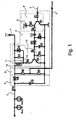
- Fig. 1 shows a circuit diagram of an inventive electric assembly.
- the electric assembly is connected between a control computer (which is part of an electric interlocking system) and a set of output relays Rel1, Rel2.
- the output relays Rel1, Rel2 control railway field devices such as railway signals according to the orders of the control computer (the details of this controlling are not shown here).
- the electric assembly is adapted to forward a constant input voltage Vin at a working input 1 to a working output 2, which is connected to the control inputs of the output relays Rel1, Rel2, as long as the control computer works properly.
- control computer As long as the control computer works properly, it provides an AC dynamic signal (such as a sinusoidal or saw tooth voltage) to a monitoring input 3 of the electric assembly.
- an AC dynamic signal such as a sinusoidal or saw tooth voltage
- the electric assembly stops the forwarding of the input voltage Vin to the working output 2 by means of a dynamic circuit 4. Nonetheless, the voltage Vrel at the working output 2 stays for some time at its level by means of a buffer circuit 5.
- the ending of the forwarding of the input voltage Vin can be noticed with the aid of a measuring circuit 6 providing a readout signal Vread to a readout output 7 before Vrel drops significantly. If the dynamic signal is reestablished quickly enough (i.e, within a "buffer time" of the buffer circuit), the input voltage Vin is forwarded again before Vrel has dropped significantly. This characteristic is used to test the electric assembly. In this case, there is no interruption of the voltage supply of the output relays Rel1, Rel2. If the dynamic signal is not reestablished quickly enough, what is in particular the case at a malfunction of the control computer, the voltage at the working output 2 finally drops. Then the output relays Rel1, Rel2 get no more (or not enough) relay voltage Vrel and switch into a safe state.
- a dynamic signal (such as a rectangular alternating voltage of e.g. 5 volts peak to peak and 10 Hz) is present at the monitoring input 3.
- the dynamic signal is provided via resistor R1 to the basis of the AC amplification transistor V1.
- V1 blocks, and the loading capacitor C1 and the switching capacitor C2 are loaded by the supply voltage Vsup of supply voltage input 8 via resistors R2, R3, and loading diode V2.
- the switching capacitor C2 provides (via resistor R4) the basis of a DC amplification transistor V4 with a voltage, so V4 becomes conductive.
- the switching transistor V7 (here a field effect transistor) gets a voltage onto its control contact 10 (here its gate).
- the voltage at the control contact 10 is limited by the limiting diode V6.
- V4, R4, R6, R7 and V6 form an amplification circuit 13 of the switching capacity C2.
- C2 is called switching capacitor.
- the regular operation is maintained for a predefined time, such as one hour or one day, and then a test procedure is launched, independent of the use of the output relays Rel1, Rel2.
- a constant high level signal is set instead of the dynamic signal.
- the AC amplification transistor V1 is conductive, and loading capacitor C1 is discharged via the discharging diode V3 and resistor R3 and V1.
- the switching capacitor C2 is not reloaded periodically any more, but discharged via the resistive components V4 and R5, and R4.
- the DC amplification transistor V4 blocks, and the control contact 10 of switching transistor V7 looses its voltage.
- the buffer capacity C3 provides the energy for the output relays Rel1, Rel2.
- separating diode V8 blocks and prevents the buffer capacity C3 from discharging via the resistors R8, R9.
- the testing can also be done with a constant low level signal at the monitoring input 3.
- C1 there is a constant voltage. Since C2 requires changing charges at C1 for further loading, C2 is discharges via R4, R5, V4 again, with the further function of the electric assembly as described above.
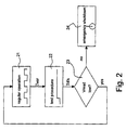
- Figure 2 describes an inventive method for operating a railway control center device, comprising an inventive electric assembly as described above, connected to a control computer and at least one output relay.
- the railway control center device is, at the beginning, in regular operation 21.
- the dynamic signal is provided to the monitoring input of the electric assembly by the monitoring output of the control computer.
- the control computer After a time interval Tver, the control computer starts automatically a test procedure 22.
- the signal at the monitoring input is put to a constant high level. Then it is waited for a time interval Tdis, long enough for the switching capacitor C2 to discharge, and the switching transistor V7 to block, but short enough so buffer capacity C3 is not yet discharged.
- Tdis the time interval for the switching capacitor C2 to discharge, and the switching transistor V7 to block, but short enough so buffer capacity C3 is not yet discharged.
- the readout signal Vout at the readout output is read out in step 23.
- Vout is at high level, indicating that the dynamic circuit does not de-energize as required for safety reasons, an emergency shutdown 24 of the input voltage Vin is undertaken.
- the voltage Vrel at the working output drops to zero, putting the output relays into a safe condition.
- the defective dynamic circuit can be repaired or exchanged afterwards,
- the invention describes a safety tool guaranteeing a turning off of a switching voltage of at least one output relay in case a control computer (or micro controller), which operates or controls the output relays, has a defect.
- a defect is indicated by the cessation of a dynamic signal which is provided to the electronic assembly.
- the electronic assembly can be tested for de-energizing independent of the use of the output relays by the control computer, and in particular as often as desired, without interfering into the regular operation of the output relays.
Landscapes
- Engineering & Computer Science (AREA)
- Mechanical Engineering (AREA)
- Testing Electric Properties And Detecting Electric Faults (AREA)
- Logic Circuits (AREA)
- Train Traffic Observation, Control, And Security (AREA)
- Fire Alarms (AREA)
Abstract
Description
- The invention relates to an electrical assembly,
in particular for an interface between an electronic interlocking system and an relay interlocking system,
wherein, in a first operating condition, the electrical assembly switches an input voltage at a working input onto a working output if an alternating voltage is applied at a monitoring input,
and wherein, in a second operating condition, the electrical assembly switches off the working output if no voltage or a direct voltage is applied to the monitoring input. - Railway control centers, i.e, interlocking systems in the railway technology, are used to control railway field devices, in particular railway signals and railway switches of railway tracks and railway stations. Since most of the controlled field devices are of safety relevance, the components of a railway control center must be verified regularly.
- In electronic railway control centers, the function of its components is checked in a cyclic manner by a test software. The checking frequency may be chosen freely, typically taking into account the technology of the components. The checking frequency is independent of the frequency of regular use of the components.
- In a relay railway control center, its relays are only checked during regular use upon engergizing and de-energizing, i.e. the checking frequency depends on the data flow.
- In the state of the art, there are also electronic interlocking systems which are attached to relay interlocking systems; this is often the result of a cost-effective partial upgrading of railway equipment. At the interface of the electronic interlocking system and the relay interlocking system, there are some electrical components which forward a switching voltage to output relays. The output relays control the railway field devices such as the railway signals or railway switches by means of the control computer. The electronic components can, in the state of the art, only be checked depending on the data flow of regular use. This may be too rare for an acceptance by common safety standards.
- More specifically, in the state of the art, there are dynamic relays connected upstream to the output relays. The control computer (belonging to the electronic interlocking system) provides electronic pulses periodically (a so called dynamic signal) when the control computer is executing its programming regularly, By means of an electronic pulse analysis, the dynamic relays are energized by the dynamic signal, and the dynamic relays can forward a switching current to the output relays. If the programming of the control computer is not executed properly and the dynamic signal ceases, the dynamic relay is supposed to de-energize, thus ending the switching current to the output relays, and putting the field devices (such as railway signals) into a safe condition.
- The electronic pulse analysis and the dynamic relays are checked periodically by a de-energizing test. However, this de-energizing for testing could be interpreted as a regular operation (such as switching a signal to red despite of a free track). This misinterpretation is prevented, in the state of the art, by doubling the pulse analysis circuit and the dynamic relays, and connecting the two sets in parallel. When one of the sets is tested, the other set can output the switching current. Such a doubling of sets is necessary for each channel of the control computer, increasing the construction costs in particular for multichannel control computers.
- It is the object of the invention to provide an electrical assembly at the interface of an electronic interlocking system and a relay interlocking system as introduced in the beginning, which allows its testing at arbitrary points of time, and at the same time is inexpensive and simple in construction.
- This object is achieved, in accordance with the invention, by an electrical assembly as introduced in the beginning, characterized in
that the electronic assembly comprises a dynamic circuit, a measurement circuit with a readout output, and a buffer circuit,
that the dynamic circuit comprises a switching capacity, which is connected to the monitoring input or an amplifier circuit of the monitoring input via a serial connection of a loading diode and a loading capacity,
wherein a resistive component is connected in parallel to the switching capacity, that the dynamic circuit further comprises a switching transistor with a first contact, a second contact and a control contact,
wherein the first contact is connected to the working input,
and wherein the control contact is connected to the switching capacity or an amplifier circuit of the switching capacity,
that the measurement circuit is connected to the second contact of the switching transistor,
and that the buffer circuit comprises a separating diode and a buffer capacity,
wherein the separating diode connects the second contact of the switching transistor with the working output,
and wherein the buffer capacity is connected to the working output. - In brief, the switching capacitor (C2) collects charges upon any recharging of the loading capacitor (C1) when the dynamic signal is present.. When enough charge is accumulated at the switching capacitor, the switching transistor (V7) becomes conductive, and forwards the input voltage to the working output. When the dynamic signal is not present, the switching capacity is no further charged, but is discharged via the resistive components (R5, V4). The switching transistor blocks. The voltage at the second contact of the switching transistor measurement circuit drops, what can be read at the readout output, indicating proper de-energizing. However, the voltage at the working output is maintained by the buffer capacity for some time, long enough to make the switching transistor conductive again (by resuming the dynamic signal) before the voltage at the working output has dropped significantly.
- The inventive electrical assembly is a completely electronic surveillance tool for the dynamic of the control computer, in particular doing without any space-consuming relays such as dynamic relays. This minimizes the risk of mechanical malfunctions. Note that dynamic relays may have malfunctions that are difficult to detect with regular testing. The switching transistor and the electronic assembly as a whole, in contrast, are much more reliable than a dynamic relay, and very easy to test.
- Further, the switching transistor is voltage controlled (and not current-controlled as a relay), and thus can be operated with less power consumption.
- Within the electrical assembly, there are no components that need to be provided in double and connected in parallel. The inventive electronic assembly itself can maintain a switching current at the interface relays during testing by means of the buffer circuit. This makes the inventive electronic assembly very cost-effective and keeps its design simple and small.
- In a preferred embodiment of the inventive electric assembly, the measurement circuit comprises a series connection of two resistors, and the readout output is attached between the two resistors. The two resistors act as potential dividers, so a typical voltage at the readout output can be set. Further, via the resistors a relic voltage at the second contact of the switching transistor is quickly eliminated during testing.
- In another preferred embodiment of the invention, the the switching transistor is a field effect transistor, in particular a VMOS transistor, and the control contact of the switching transistor is the gate of the field effect transistor. The field effect transistor is voltage controlled, and only little electric power at the control contact is sufficient for controlling the forwarding of voltage.
- Further preferred is an embodiment of the inventive electrical assembly wherein the control contact of the switching transistor is connected to the working input via a resistor, or a limiting diode, or a resistor and a limiting diode connected in parallel. By these means, in particular with the limiting diode, the voltage at the control input of the switching transistor can be limited to a maximum value appropriate for the switching transistor.
- Further preferred is an embodiment wherein the switching capacity is connected to the basis of a DC amplification transistor via a resistor, and the collector of the DC amplification transistor is connected to the control contact of the switching transistor via a resistor. By this means, the current resulting from the charge at the switching capacity through the resistive component, here the DC amplification transistor, can be amplified in order to switch the state of the switching transistor.
- In a preferred further development of this embodiment, the basis of the DC amplification transistor is connected to a grounded resistor. With the grounded resistor, a relic voltage at the switching capacity can be eliminated more quickly. It further helps setting the amplification factor at the DC amplification transistor.
- In a preferred embodiment, the electrical assembly is characterized in
that the monitoring input is connected to the basis of an AC amplification transistor via a resistor,
that the collector of the AC amplification transistor is connected to a supply voltage input via a resistor,
and that the collector of the AC amplification transistor is connected to the loading capacitor, in particular via a resistor. By this means, the signal at the monitoring input is amplified in order to allow or accelerate the loading of the switching capacity. A typical voltage at the supply voltage input is 5 V DC. The resistor (R3) upstream of the loading capacitor helps to avoid current peaks. - Another advantageous embodiment provides that a grounded discharging diode is attached between the loading diode and the loading capacity. The discharging diode helps to discharge the loading capacity during testing.
- Also within the scope of the invention is a railway control center device, comprising at least one output relay for a railway field device such as a railway signal or a track switch, and a control computer for controlling the at least one relay, wherein the control computer has a monitoring output for providing an alternating voltage signal in order to indicate its proper working condition, characterized in that the railway control center device further comprises an inventive electric assembly (or one of its embodiments mentioned above),
wherein the at least one output relay has a control input which is connected to the working output of the electric assembly, and wherein the monitoring output of the control computer is connected to the monitoring input of the electric assembly. The inventive railway control center device can secure the at least one output relay, and it can be tested whenever desired, in particular periodically and independent from regular use, without interfering into the regular use when testing. - Further within the scope of the invention is a method for operating a railway control center device as described above, characterized in that the control computer periodically runs a testing program, with the following steps:
- a) a direct current signal or no signal is applied to the monitoring output of the control computer;
- b) if the signal at the readout output of the measurement circuit drops to low level within a predefined time interval, indicating a proper functioning of the dynamic circuit, an alternating voltage signal is provided at the monitoring output of the control computer again until the next cycle of the testing program;
- c) if the signal at the readout output does not drop to low level within a predefined time interval, indicating a malfunction of the dynamic circuit, an error message is delivered and/or an emergency shutdown of the voltage at the control input of the at least one output relay is done. With this procedure, the railway control center device can be tested in a to the satisfaction of any safety standard, in particular as often as necessary.
- Further advantages can be extracted from the description and the enclosed drawing. The features mentioned above and below can be used in accordance with the invention either individually or collectively in any combination. The embodiments mentioned are not to be understood as exhaustive enumeration but rather have exemplary character for the description of the invention.
- The invention is shown in the drawing.
- Fig. 1
- shows a circuit diagram of an inventive electric assembly;
- Fig. 2
- shows a flow diagram of an inventive method for operating a railroad control center device comprising an inventive electric assembly.
- Fig. 1 shows a circuit diagram of an inventive electric assembly. The electric assembly is connected between a control computer (which is part of an electric interlocking system) and a set of output relays Rel1, Rel2. The output relays Rel1, Rel2 control railway field devices such as railway signals according to the orders of the control computer (the details of this controlling are not shown here). The electric assembly is adapted to forward a constant input voltage Vin at a working
input 1 to a working output 2, which is connected to the control inputs of the output relays Rel1, Rel2, as long as the control computer works properly. - As long as the control computer works properly, it provides an AC dynamic signal (such as a sinusoidal or saw tooth voltage) to a
monitoring input 3 of the electric assembly. When the dynamic signal ceases (by staying at a constant level which may be zero or a higher voltage), the electric assembly stops the forwarding of the input voltage Vin to the working output 2 by means of a dynamic circuit 4. Nonetheless, the voltage Vrel at the working output 2 stays for some time at its level by means of abuffer circuit 5. - The ending of the forwarding of the input voltage Vin can be noticed with the aid of a measuring circuit 6 providing a readout signal Vread to a readout output 7 before Vrel drops significantly. If the dynamic signal is reestablished quickly enough (i.e, within a "buffer time" of the buffer circuit), the input voltage Vin is forwarded again before Vrel has dropped significantly. This characteristic is used to test the electric assembly. In this case, there is no interruption of the voltage supply of the output relays Rel1, Rel2. If the dynamic signal is not reestablished quickly enough, what is in particular the case at a malfunction of the control computer, the voltage at the working output 2 finally drops. Then the output relays Rel1, Rel2 get no more (or not enough) relay voltage Vrel and switch into a safe state.
- In the following, the function of the inventive electric assembly is explained in detail.
- During regular operation, a dynamic signal (such as a rectangular alternating voltage of e.g. 5 volts peak to peak and 10 Hz) is present at the
monitoring input 3. The dynamic signal is provided via resistor R1 to the basis of the AC amplification transistor V1. - When the dynamic signal is in a low voltage half wave, V1 blocks, and the loading capacitor C1 and the switching capacitor C2 are loaded by the supply voltage Vsup of
supply voltage input 8 via resistors R2, R3, and loading diode V2. - When the dynamic signal is in a high voltage half wave, then the AC amplification transistor V1 is conducting, and loading capacitor C1 is discharged via discharging diode V3 as well as resistors R3 and V1.
- When V1 blocks again, C1 is recharged, and C2 is charged further. After a few cycles of the dynamic signal, a saturation voltage of e.g. 2V is present at the switching capacitor C2. In this sense, C1 loads C2, therefore C1 is called loading capacitor. Note that the
supply voltage input 8, the resistors R1, R2, R3, and AC amplification transistor V1 form an amplifier circuit 9 for themonitoring input 3. - The switching capacitor C2 provides (via resistor R4) the basis of a DC amplification transistor V4 with a voltage, so V4 becomes conductive. Via the potential divider of the two resistors R6, R7 connected to the working
input 1, the switching transistor V7 (here a field effect transistor) gets a voltage onto its control contact 10 (here its gate). The voltage at thecontrol contact 10 is limited by the limiting diode V6. V4, R4, R6, R7 and V6 form anamplification circuit 13 of the switching capacity C2. - As a consequence of the voltage at the
control contact 10, the switching transistor V7 becomes conductive, and the input voltage Vin at thefirst contact 11 is transmitted to thesecond contact 12 as well as to the working output 2 via the separating diode V8, so a voltage Vrel equaling Vin is present at the working output 2. In the end, it is the voltage at C2 that causes the switching transistor V7 to change its state. Therefore, C2 is called switching capacitor. - The buffer capacity C3, which is connected to the working output 2, is loaded. Moreover, the potential divider of the resistors R8, R9 connected to the
second contact 12 of V7 provides a high voltage level to the readout output 7. - Typically, and in accordance with the invention, the regular operation is maintained for a predefined time, such as one hour or one day, and then a test procedure is launched, independent of the use of the output relays Rel1, Rel2.
- For testing the dynamic circuit 4, at the monitoring input 3 a constant high level signal is set instead of the dynamic signal. As a result, the AC amplification transistor V1 is conductive, and loading capacitor C1 is discharged via the discharging diode V3 and resistor R3 and V1. The switching capacitor C2 is not reloaded periodically any more, but discharged via the resistive components V4 and R5, and R4. The DC amplification transistor V4 blocks, and the
control contact 10 of switching transistor V7 looses its voltage. - As a result of the lacking voltage at the
control input 10, the V7 blocks. At the anode of V8 (or at thesecond contact 12 of V7), there is no more voltage either. Note that any relic voltage there would be discharged via R8, R9. As a result, the readout signal Vread at readout output 7 drops to low level (here even zero level). - As soon as there is a low level at the readout output 7, the proper de-energizing function of the dynamic circuit 4 is proved, and the control computer immediately reestablishes the regular dynamic signal. Quickly afterwards, V7 is conductive again.
- For the duration of a successful testing, i.e. from the beginning of the constant high level signal at monitoring
input 3 until the V7 becomes conductive again, the buffer capacity C3 provides the energy for the output relays Rel1, Rel2. During the testing, separating diode V8 blocks and prevents the buffer capacity C3 from discharging via the resistors R8, R9. - The testing can also be done with a constant low level signal at the
monitoring input 3. At C1, there is a constant voltage. Since C2 requires changing charges at C1 for further loading, C2 is discharges via R4, R5, V4 again, with the further function of the electric assembly as described above. - Figure 2 describes an inventive method for operating a railway control center device, comprising an inventive electric assembly as described above, connected to a control computer and at least one output relay.
- The railway control center device is, at the beginning, in
regular operation 21. During regular operation, the dynamic signal is provided to the monitoring input of the electric assembly by the monitoring output of the control computer. - After a time interval Tver, the control computer starts automatically a
test procedure 22. The signal at the monitoring input is put to a constant high level. Then it is waited for a time interval Tdis, long enough for the switching capacitor C2 to discharge, and the switching transistor V7 to block, but short enough so buffer capacity C3 is not yet discharged. Immediately after Tdis has elapsed, the readout signal Vout at the readout output is read out instep 23. - If Vout is at low level, indicating proper de-energizing of the dynamic circuit,
regular operation 21 is resumed for another time interval Tver. - If Vout is at high level, indicating that the dynamic circuit does not de-energize as required for safety reasons, an
emergency shutdown 24 of the input voltage Vin is undertaken. The voltage Vrel at the working output drops to zero, putting the output relays into a safe condition. The defective dynamic circuit can be repaired or exchanged afterwards, - In summary, the invention describes a safety tool guaranteeing a turning off of a switching voltage of at least one output relay in case a control computer (or micro controller), which operates or controls the output relays, has a defect. Such a defect is indicated by the cessation of a dynamic signal which is provided to the electronic assembly. The electronic assembly can be tested for de-energizing independent of the use of the output relays by the control computer, and in particular as often as desired, without interfering into the regular operation of the output relays.
Claims (10)
- Electrical assembly,
in particular for an interface between an electronic interlocking system and a relay interlocking system,
wherein, in a first operating condition, the electrical assembly switches an input voltage (Vin) at a working input (1) onto a working output (2) if an alternating voltage is applied at a monitoring input (3),
and wherein, in a second operating condition, the electrical assembly switches off the working output (2) if no voltage or a direct voltage is applied to the monitoring input (3),
characterized in
that the electronic assembly comprises a dynamic circuit (4), a measurement circuit (6) with a readout output (7), and a buffer circuit (5), that the dynamic circuit (4) comprises a switching capacity (C2), which is connected to the monitoring input (3) or an amplifier circuit (9) of the monitoring input (3) via a serial connection of a loading diode (V2) and a loading capacity (C1),
wherein a resistive component (R5, V4) is connected in parallel to the switching capacity (C2),
that the dynamic circuit (4) further comprises a switching transistor (V7) with a first contact(11), a second contact (12) and a control contact (10),
wherein the first contact (11) is connected to the working input (1),
and wherein the control contact (10) is connected to the switching capacity (C2) or an amplifier circuit (13) of the switching capacity (C2), that the measurement circuit (6) is connected to the second contact (12) of the switching transistor (V7),
and that the buffer circuit (5) comprises a separating diode (V8) and a buffer capacity (C3),
wherein the separating diode (V8) connects the second contact (12) of the switching transistor (V7) with the working output (2),
and wherein the buffer capacity (C3) is connected to the working output (2). - Electric assembly according to claim 1, characterized in that the measurement circuit (6) comprises a series connection of two resistors (R8, R9), and the readout output (7) is attached between the two resistors (R8, R9).
- Electric assembly according to claim 1, characterized in that the switching transistor (V7) is a field effect transistor, in particular a VMOS transistor, and the control contact (10) of the switching transistor (V7) is the gate of the field effect transistor.
- Electrical assembly according to claim 1, characterized in that the control contact (10) of the switching transistor (V7) is connected to the working input (1) via a resistor (R7), or a limiting diode (V6), or a resistor (R7) and a limiting diode (V6) connected in parallel.
- Electrical assembly according to claim 1, characterized in that the switching capacity (C2) is connected to the basis of a DC amplification transistor (V4) via a resistor (R4), and the collector of the DC amplification transistor (V4) is connected to the control contact (10) of the switching transistor (V7) via a resistor (R6).
- Electrical assembly according to claim 5, characterized in that the basis of the DC amplification transistor (V4) is connected to a grounded resistor (R5).
- Electrical assembly according to claim 1, characterized in
that the monitoring input (3) is connected to the basis of an AC amplification transistor (V1) via a resistor (R1),
that the collector of the AC amplification transistor (V1) is connected to a supply voltage input (8) via a resistor (R2),
and that the collector of the AC amplification transistor (V1) is connected to the loading capacitor (C1), in particular via a resistor (R3). - Electrical assembly according to claim 1, characterized in that a grounded discharging diode (V3) is attached between the loading diode (V2) and the loading capacity (C1).
- Railway control center device, comprising
at least one output relay (Rel1, Rel2) for a railway field device such as a railway signal or a track switch,
and a control computer for controlling the at least one output relay (Rel1, Rel2),
wherein the control computer has a monitoring output for providing an alternating voltage signal in order to indicate its proper working condition,
characterized in
that the railway control center device further comprises an electric assembly according to claim 1,
wherein the at least one output relay (Rel1, Rel2) has a control input which is connected to the working output (2) of the electric assembly, and wherein the monitoring output of the control computer is connected to the monitoring input (3) of the electric assembly. - Method for operating a railway control center device according to claim 9,
characterized in that the control computer periodically runs a testing program, with the following steps:a) a direct current signal or no signal is applied to the monitoring output of the control computer (22);b) if the signal at the readout output of the measurement circuit drops to low level within a predefined time interval (Tdis), indicating a proper functioning of the dynamic circuit (4), an alternating voltage signal is provided at the monitoring output of the control computer again until the next cycle of the testing program (21);c) if the signal at the readout output (7) does not drop to low level within a predefined time interval (Tdis), indicating a malfunction of the dynamic circuit (4), an error message is delivered and/or an emergency shutdown (24) of the voltage at the control input of the at least one output relay (Rel1, Rel2) is done.
Priority Applications (3)
| Application Number | Priority Date | Filing Date | Title |
|---|---|---|---|
| DE602006002370T DE602006002370D1 (en) | 2006-05-10 | 2006-05-10 | Electrical circuit for monitoring the interface between an electronic interlocking and a relay interlocking |
| EP06290777A EP1854697B1 (en) | 2006-05-10 | 2006-05-10 | Electric assembly for monitoring the interface between an electronic interlocking system and a relay interlocking system |
| AT06290777T ATE405470T1 (en) | 2006-05-10 | 2006-05-10 | ELECTRICAL CIRCUIT FOR MONITORING THE INTERFACE BETWEEN AN ELECTRONIC INTERLOCKING AND A RELAY INTERLOCKING |
Applications Claiming Priority (1)
| Application Number | Priority Date | Filing Date | Title |
|---|---|---|---|
| EP06290777A EP1854697B1 (en) | 2006-05-10 | 2006-05-10 | Electric assembly for monitoring the interface between an electronic interlocking system and a relay interlocking system |
Publications (2)
| Publication Number | Publication Date |
|---|---|
| EP1854697A1 true EP1854697A1 (en) | 2007-11-14 |
| EP1854697B1 EP1854697B1 (en) | 2008-08-20 |
Family
ID=37025196
Family Applications (1)
| Application Number | Title | Priority Date | Filing Date |
|---|---|---|---|
| EP06290777A Not-in-force EP1854697B1 (en) | 2006-05-10 | 2006-05-10 | Electric assembly for monitoring the interface between an electronic interlocking system and a relay interlocking system |
Country Status (3)
| Country | Link |
|---|---|
| EP (1) | EP1854697B1 (en) |
| AT (1) | ATE405470T1 (en) |
| DE (1) | DE602006002370D1 (en) |
Cited By (1)
| Publication number | Priority date | Publication date | Assignee | Title |
|---|---|---|---|---|
| CN116039710A (en) * | 2022-11-28 | 2023-05-02 | 通号城市轨道交通技术有限公司 | Interface circuit for full-electronic computer interlocking and relay centralized interlocking and communication method |
Citations (2)
| Publication number | Priority date | Publication date | Assignee | Title |
|---|---|---|---|---|
| DE3743755A1 (en) * | 1987-12-23 | 1989-07-06 | Standard Elektrik Lorenz Ag | Method for transferring block information between geographical circuit installations |
| EP0787639A1 (en) * | 1996-02-02 | 1997-08-06 | Siemens Schweiz AG | Arrangement for connecting an electronic interlocking system to a relay interlocking system |
-
2006
- 2006-05-10 DE DE602006002370T patent/DE602006002370D1/en active Active
- 2006-05-10 EP EP06290777A patent/EP1854697B1/en not_active Not-in-force
- 2006-05-10 AT AT06290777T patent/ATE405470T1/en not_active IP Right Cessation
Patent Citations (2)
| Publication number | Priority date | Publication date | Assignee | Title |
|---|---|---|---|---|
| DE3743755A1 (en) * | 1987-12-23 | 1989-07-06 | Standard Elektrik Lorenz Ag | Method for transferring block information between geographical circuit installations |
| EP0787639A1 (en) * | 1996-02-02 | 1997-08-06 | Siemens Schweiz AG | Arrangement for connecting an electronic interlocking system to a relay interlocking system |
Non-Patent Citations (3)
| Title |
|---|
| BLECHINGER H-J: "EB L2000 - ELEKTRONISCHE BLOCKTECHNIK FUER CIR-ELKE-STRECKEN", SIGNAL + DRAHT, TELZLAFF VERLAG GMBH. DARMSTADT, DE, vol. 87, no. 3, March 1995 (1995-03-01), pages 80 - 83, XP002016086, ISSN: 0037-4997 * |
| LENNARTZ K ET AL: "BEDIENUNG VON RELAISSTELLWERKEN AUS ESTW", SIGNAL + DRAHT, TELZLAFF VERLAG GMBH. DARMSTADT, DE, vol. 85, no. 4, 1 April 1993 (1993-04-01), pages 126 - 130, XP000380311, ISSN: 0037-4997 * |
| RAHN ET AL: "Integration von Relaisstellwerken in die Bedienoberfläche des ESTW L90", SIGNAL + DRAHT, TELZLAFF VERLAG GMBH. DARMSTADT, DE, vol. 93, no. 4, April 2001 (2001-04-01), pages 24 - 26, XP002348969, ISSN: 0037-4997 * |
Cited By (1)
| Publication number | Priority date | Publication date | Assignee | Title |
|---|---|---|---|---|
| CN116039710A (en) * | 2022-11-28 | 2023-05-02 | 通号城市轨道交通技术有限公司 | Interface circuit for full-electronic computer interlocking and relay centralized interlocking and communication method |
Also Published As
| Publication number | Publication date |
|---|---|
| EP1854697B1 (en) | 2008-08-20 |
| DE602006002370D1 (en) | 2008-10-02 |
| ATE405470T1 (en) | 2008-09-15 |
Similar Documents
| Publication | Publication Date | Title |
|---|---|---|
| US6437540B2 (en) | Battery pack | |
| EP3565073B1 (en) | Self-test of over-current fault detection | |
| CN104386091B (en) | A rail transit safety control circuit and system | |
| US9640980B2 (en) | Power interrupting device | |
| EP1465319B1 (en) | Uninterruptible power supply device with circuit for degradation judgment of storage battery | |
| US8878552B2 (en) | End-of-line capacitor for measuring wiring impedance of emergency notification circuits | |
| EP2410644A1 (en) | A half bridge and half bridge control method | |
| CN102955136A (en) | Assistant detection circuit and assistant detection method for redundant power sources | |
| CN114614448B (en) | DC Switch | |
| CN104467156B (en) | Automatic repair system for power supplies | |
| US8044638B2 (en) | Monitoring system for monitoring low voltage disconnecting value of secondary batteries and method for the same | |
| JP2016134832A (en) | Load drive circuit | |
| CN107430172B (en) | Battery monitoring apparatus and method using discharge pulse measurements | |
| EP1854697B1 (en) | Electric assembly for monitoring the interface between an electronic interlocking system and a relay interlocking system | |
| CN107621566B (en) | Voltage detection equipment and voltage detection method | |
| EP2546852A2 (en) | Bi-stable security relay | |
| CN112838848A (en) | An insulated gate bipolar transistor series valve structure | |
| US20140211352A1 (en) | Protection apparatus and control method for the same | |
| EP3509178B1 (en) | Diagnostic system for vehicle electrical system having dc-dc voltage converter and voltage regulator | |
| JP4802740B2 (en) | Timer circuit and charge control device | |
| US11258299B1 (en) | Generating charge for service disconnect operation | |
| CN112595905B (en) | Circuit and method for real-time detection of faulty capacitors | |
| CN118100115B (en) | Protection circuit, method and related equipment for preventing current from flowing backwards | |
| CN101938116A (en) | Relay protection method and device | |
| EP2782112A1 (en) | Monitoring and control system comprising a safety switch and method for operating a safety switch |
Legal Events
| Date | Code | Title | Description |
|---|---|---|---|
| PUAI | Public reference made under article 153(3) epc to a published international application that has entered the european phase |
Free format text: ORIGINAL CODE: 0009012 |
|
| AK | Designated contracting states |
Kind code of ref document: A1 Designated state(s): AT BE BG CH CY CZ DE DK EE ES FI FR GB GR HU IE IS IT LI LT LU LV MC NL PL PT RO SE SI SK TR |
|
| AX | Request for extension of the european patent |
Extension state: AL BA HR MK YU |
|
| 17P | Request for examination filed |
Effective date: 20071108 |
|
| RTI1 | Title (correction) |
Free format text: ELECTRIC ASSEMBLY FOR MONITORING THE INTERFACE BETWEEN AN ELECTRONIC INTERLOCKING SYSTEM AND A RELAY INTERLOCKING SYSTEM |
|
| GRAP | Despatch of communication of intention to grant a patent |
Free format text: ORIGINAL CODE: EPIDOSNIGR1 |
|
| GRAS | Grant fee paid |
Free format text: ORIGINAL CODE: EPIDOSNIGR3 |
|
| GRAA | (expected) grant |
Free format text: ORIGINAL CODE: 0009210 |
|
| AKX | Designation fees paid |
Designated state(s): AT BE BG CH CY CZ DE DK EE ES FI FR GB GR HU IE IS IT LI LT LU LV MC NL PL PT RO SE SI SK TR |
|
| AK | Designated contracting states |
Kind code of ref document: B1 Designated state(s): AT BE BG CH CY CZ DE DK EE ES FI FR GB GR HU IE IS IT LI LT LU LV MC NL PL PT RO SE SI SK TR |
|
| REG | Reference to a national code |
Ref country code: GB Ref legal event code: FG4D |
|
| REG | Reference to a national code |
Ref country code: CH Ref legal event code: EP |
|
| REG | Reference to a national code |
Ref country code: IE Ref legal event code: FG4D |
|
| REF | Corresponds to: |
Ref document number: 602006002370 Country of ref document: DE Date of ref document: 20081002 Kind code of ref document: P |
|
| PG25 | Lapsed in a contracting state [announced via postgrant information from national office to epo] |
Ref country code: LT Free format text: LAPSE BECAUSE OF FAILURE TO SUBMIT A TRANSLATION OF THE DESCRIPTION OR TO PAY THE FEE WITHIN THE PRESCRIBED TIME-LIMIT Effective date: 20080820 Ref country code: IS Free format text: LAPSE BECAUSE OF FAILURE TO SUBMIT A TRANSLATION OF THE DESCRIPTION OR TO PAY THE FEE WITHIN THE PRESCRIBED TIME-LIMIT Effective date: 20081220 Ref country code: NL Free format text: LAPSE BECAUSE OF FAILURE TO SUBMIT A TRANSLATION OF THE DESCRIPTION OR TO PAY THE FEE WITHIN THE PRESCRIBED TIME-LIMIT Effective date: 20080820 |
|
| PG25 | Lapsed in a contracting state [announced via postgrant information from national office to epo] |
Ref country code: ES Free format text: LAPSE BECAUSE OF FAILURE TO SUBMIT A TRANSLATION OF THE DESCRIPTION OR TO PAY THE FEE WITHIN THE PRESCRIBED TIME-LIMIT Effective date: 20081201 Ref country code: FI Free format text: LAPSE BECAUSE OF FAILURE TO SUBMIT A TRANSLATION OF THE DESCRIPTION OR TO PAY THE FEE WITHIN THE PRESCRIBED TIME-LIMIT Effective date: 20080820 Ref country code: AT Free format text: LAPSE BECAUSE OF FAILURE TO SUBMIT A TRANSLATION OF THE DESCRIPTION OR TO PAY THE FEE WITHIN THE PRESCRIBED TIME-LIMIT Effective date: 20080820 Ref country code: SI Free format text: LAPSE BECAUSE OF FAILURE TO SUBMIT A TRANSLATION OF THE DESCRIPTION OR TO PAY THE FEE WITHIN THE PRESCRIBED TIME-LIMIT Effective date: 20080820 Ref country code: LV Free format text: LAPSE BECAUSE OF FAILURE TO SUBMIT A TRANSLATION OF THE DESCRIPTION OR TO PAY THE FEE WITHIN THE PRESCRIBED TIME-LIMIT Effective date: 20080820 |
|
| PG25 | Lapsed in a contracting state [announced via postgrant information from national office to epo] |
Ref country code: BE Free format text: LAPSE BECAUSE OF FAILURE TO SUBMIT A TRANSLATION OF THE DESCRIPTION OR TO PAY THE FEE WITHIN THE PRESCRIBED TIME-LIMIT Effective date: 20080820 |
|
| PG25 | Lapsed in a contracting state [announced via postgrant information from national office to epo] |
Ref country code: BG Free format text: LAPSE BECAUSE OF FAILURE TO SUBMIT A TRANSLATION OF THE DESCRIPTION OR TO PAY THE FEE WITHIN THE PRESCRIBED TIME-LIMIT Effective date: 20081120 Ref country code: DK Free format text: LAPSE BECAUSE OF FAILURE TO SUBMIT A TRANSLATION OF THE DESCRIPTION OR TO PAY THE FEE WITHIN THE PRESCRIBED TIME-LIMIT Effective date: 20080820 |
|
| PG25 | Lapsed in a contracting state [announced via postgrant information from national office to epo] |
Ref country code: SK Free format text: LAPSE BECAUSE OF FAILURE TO SUBMIT A TRANSLATION OF THE DESCRIPTION OR TO PAY THE FEE WITHIN THE PRESCRIBED TIME-LIMIT Effective date: 20080820 Ref country code: PT Free format text: LAPSE BECAUSE OF FAILURE TO SUBMIT A TRANSLATION OF THE DESCRIPTION OR TO PAY THE FEE WITHIN THE PRESCRIBED TIME-LIMIT Effective date: 20090120 Ref country code: RO Free format text: LAPSE BECAUSE OF FAILURE TO SUBMIT A TRANSLATION OF THE DESCRIPTION OR TO PAY THE FEE WITHIN THE PRESCRIBED TIME-LIMIT Effective date: 20080820 Ref country code: CZ Free format text: LAPSE BECAUSE OF FAILURE TO SUBMIT A TRANSLATION OF THE DESCRIPTION OR TO PAY THE FEE WITHIN THE PRESCRIBED TIME-LIMIT Effective date: 20080820 |
|
| PLBE | No opposition filed within time limit |
Free format text: ORIGINAL CODE: 0009261 |
|
| STAA | Information on the status of an ep patent application or granted ep patent |
Free format text: STATUS: NO OPPOSITION FILED WITHIN TIME LIMIT |
|
| 26N | No opposition filed |
Effective date: 20090525 |
|
| PG25 | Lapsed in a contracting state [announced via postgrant information from national office to epo] |
Ref country code: EE Free format text: LAPSE BECAUSE OF FAILURE TO SUBMIT A TRANSLATION OF THE DESCRIPTION OR TO PAY THE FEE WITHIN THE PRESCRIBED TIME-LIMIT Effective date: 20080820 |
|
| PG25 | Lapsed in a contracting state [announced via postgrant information from national office to epo] |
Ref country code: MC Free format text: LAPSE BECAUSE OF NON-PAYMENT OF DUE FEES Effective date: 20090531 |
|
| PG25 | Lapsed in a contracting state [announced via postgrant information from national office to epo] |
Ref country code: SE Free format text: LAPSE BECAUSE OF FAILURE TO SUBMIT A TRANSLATION OF THE DESCRIPTION OR TO PAY THE FEE WITHIN THE PRESCRIBED TIME-LIMIT Effective date: 20081120 |
|
| REG | Reference to a national code |
Ref country code: IE Ref legal event code: MM4A |
|
| PG25 | Lapsed in a contracting state [announced via postgrant information from national office to epo] |
Ref country code: IE Free format text: LAPSE BECAUSE OF NON-PAYMENT OF DUE FEES Effective date: 20090510 |
|
| PG25 | Lapsed in a contracting state [announced via postgrant information from national office to epo] |
Ref country code: PL Free format text: LAPSE BECAUSE OF FAILURE TO SUBMIT A TRANSLATION OF THE DESCRIPTION OR TO PAY THE FEE WITHIN THE PRESCRIBED TIME-LIMIT Effective date: 20080820 |
|
| PG25 | Lapsed in a contracting state [announced via postgrant information from national office to epo] |
Ref country code: GR Free format text: LAPSE BECAUSE OF FAILURE TO SUBMIT A TRANSLATION OF THE DESCRIPTION OR TO PAY THE FEE WITHIN THE PRESCRIBED TIME-LIMIT Effective date: 20081121 |
|
| REG | Reference to a national code |
Ref country code: CH Ref legal event code: PL |
|
| PG25 | Lapsed in a contracting state [announced via postgrant information from national office to epo] |
Ref country code: LI Free format text: LAPSE BECAUSE OF NON-PAYMENT OF DUE FEES Effective date: 20100531 Ref country code: CH Free format text: LAPSE BECAUSE OF NON-PAYMENT OF DUE FEES Effective date: 20100531 |
|
| PG25 | Lapsed in a contracting state [announced via postgrant information from national office to epo] |
Ref country code: LU Free format text: LAPSE BECAUSE OF NON-PAYMENT OF DUE FEES Effective date: 20090510 |
|
| PG25 | Lapsed in a contracting state [announced via postgrant information from national office to epo] |
Ref country code: HU Free format text: LAPSE BECAUSE OF FAILURE TO SUBMIT A TRANSLATION OF THE DESCRIPTION OR TO PAY THE FEE WITHIN THE PRESCRIBED TIME-LIMIT Effective date: 20090221 |
|
| PG25 | Lapsed in a contracting state [announced via postgrant information from national office to epo] |
Ref country code: TR Free format text: LAPSE BECAUSE OF FAILURE TO SUBMIT A TRANSLATION OF THE DESCRIPTION OR TO PAY THE FEE WITHIN THE PRESCRIBED TIME-LIMIT Effective date: 20080820 |
|
| PG25 | Lapsed in a contracting state [announced via postgrant information from national office to epo] |
Ref country code: CY Free format text: LAPSE BECAUSE OF FAILURE TO SUBMIT A TRANSLATION OF THE DESCRIPTION OR TO PAY THE FEE WITHIN THE PRESCRIBED TIME-LIMIT Effective date: 20080820 |
|
| REG | Reference to a national code |
Ref country code: FR Ref legal event code: PLFP Year of fee payment: 10 |
|
| PGFP | Annual fee paid to national office [announced via postgrant information from national office to epo] |
Ref country code: GB Payment date: 20150506 Year of fee payment: 10 Ref country code: DE Payment date: 20150512 Year of fee payment: 10 |
|
| PGFP | Annual fee paid to national office [announced via postgrant information from national office to epo] |
Ref country code: FR Payment date: 20150508 Year of fee payment: 10 Ref country code: IT Payment date: 20150526 Year of fee payment: 10 |
|
| REG | Reference to a national code |
Ref country code: DE Ref legal event code: R119 Ref document number: 602006002370 Country of ref document: DE |
|
| GBPC | Gb: european patent ceased through non-payment of renewal fee |
Effective date: 20160510 |
|
| PG25 | Lapsed in a contracting state [announced via postgrant information from national office to epo] |
Ref country code: IT Free format text: LAPSE BECAUSE OF NON-PAYMENT OF DUE FEES Effective date: 20160510 |
|
| REG | Reference to a national code |
Ref country code: FR Ref legal event code: ST Effective date: 20170131 |
|
| PG25 | Lapsed in a contracting state [announced via postgrant information from national office to epo] |
Ref country code: FR Free format text: LAPSE BECAUSE OF NON-PAYMENT OF DUE FEES Effective date: 20160531 Ref country code: DE Free format text: LAPSE BECAUSE OF NON-PAYMENT OF DUE FEES Effective date: 20161201 |
|
| PG25 | Lapsed in a contracting state [announced via postgrant information from national office to epo] |
Ref country code: GB Free format text: LAPSE BECAUSE OF NON-PAYMENT OF DUE FEES Effective date: 20160510 |