EP1854553A1 - Electronic device substrate, method for manufacturing substrate, compound used for substrate, method for manufacturing compound and polymerization initiator including compound - Google Patents
Electronic device substrate, method for manufacturing substrate, compound used for substrate, method for manufacturing compound and polymerization initiator including compound Download PDFInfo
- Publication number
- EP1854553A1 EP1854553A1 EP20070251888 EP07251888A EP1854553A1 EP 1854553 A1 EP1854553 A1 EP 1854553A1 EP 20070251888 EP20070251888 EP 20070251888 EP 07251888 A EP07251888 A EP 07251888A EP 1854553 A1 EP1854553 A1 EP 1854553A1
- Authority
- EP
- European Patent Office
- Prior art keywords
- compound
- group
- general formula
- electronic device
- substrate
- Prior art date
- Legal status (The legal status is an assumption and is not a legal conclusion. Google has not performed a legal analysis and makes no representation as to the accuracy of the status listed.)
- Granted
Links
- 150000001875 compounds Chemical class 0.000 title claims abstract description 161
- 239000000758 substrate Substances 0.000 title claims abstract description 116
- 238000000034 method Methods 0.000 title claims description 23
- 238000004519 manufacturing process Methods 0.000 title claims description 19
- 239000003505 polymerization initiator Substances 0.000 title claims description 12
- 238000006116 polymerization reaction Methods 0.000 claims abstract description 61
- 230000000977 initiatory effect Effects 0.000 claims abstract description 47
- 229910052751 metal Inorganic materials 0.000 claims abstract description 39
- 239000002184 metal Substances 0.000 claims abstract description 39
- 229910044991 metal oxide Inorganic materials 0.000 claims abstract description 28
- 150000004706 metal oxides Chemical class 0.000 claims abstract description 28
- 125000004430 oxygen atom Chemical group O* 0.000 claims abstract description 19
- 125000006239 protecting group Chemical group 0.000 claims abstract description 17
- 125000002947 alkylene group Chemical group 0.000 claims abstract description 15
- 125000004435 hydrogen atom Chemical group [H]* 0.000 claims abstract description 13
- 229910052717 sulfur Inorganic materials 0.000 claims description 14
- PCHJSUWPFVWCPO-UHFFFAOYSA-N gold Chemical compound [Au] PCHJSUWPFVWCPO-UHFFFAOYSA-N 0.000 claims description 12
- 229910052737 gold Inorganic materials 0.000 claims description 12
- 239000010931 gold Substances 0.000 claims description 12
- 125000004434 sulfur atom Chemical group 0.000 claims description 12
- BASFCYQUMIYNBI-UHFFFAOYSA-N platinum Chemical compound [Pt] BASFCYQUMIYNBI-UHFFFAOYSA-N 0.000 claims description 10
- 125000005843 halogen group Chemical group 0.000 claims description 6
- BQCADISMDOOEFD-UHFFFAOYSA-N Silver Chemical compound [Ag] BQCADISMDOOEFD-UHFFFAOYSA-N 0.000 claims description 5
- 229910052697 platinum Inorganic materials 0.000 claims description 5
- 229910052709 silver Inorganic materials 0.000 claims description 5
- 239000004332 silver Substances 0.000 claims description 5
- 239000011593 sulfur Substances 0.000 claims description 3
- 125000003837 (C1-C20) alkyl group Chemical group 0.000 claims 5
- 125000000217 alkyl group Chemical group 0.000 abstract description 14
- -1 perfluoro Chemical group 0.000 description 33
- 239000010410 layer Substances 0.000 description 24
- YMWUJEATGCHHMB-UHFFFAOYSA-N Dichloromethane Chemical compound ClCCl YMWUJEATGCHHMB-UHFFFAOYSA-N 0.000 description 21
- 239000002585 base Substances 0.000 description 16
- 238000006243 chemical reaction Methods 0.000 description 15
- LFQSCWFLJHTTHZ-UHFFFAOYSA-N Ethanol Chemical compound CCO LFQSCWFLJHTTHZ-UHFFFAOYSA-N 0.000 description 12
- 239000000463 material Substances 0.000 description 11
- 239000000243 solution Substances 0.000 description 11
- ZMXDDKWLCZADIW-UHFFFAOYSA-N N,N-Dimethylformamide Chemical compound CN(C)C=O ZMXDDKWLCZADIW-UHFFFAOYSA-N 0.000 description 9
- 239000007810 chemical reaction solvent Substances 0.000 description 8
- 230000035699 permeability Effects 0.000 description 7
- 125000006850 spacer group Chemical group 0.000 description 7
- 238000003786 synthesis reaction Methods 0.000 description 7
- 0 CCC(C)(*N)C(C)(C)N Chemical compound CCC(C)(*N)C(C)(C)N 0.000 description 6
- IAZDPXIOMUYVGZ-UHFFFAOYSA-N Dimethylsulphoxide Chemical compound CS(C)=O IAZDPXIOMUYVGZ-UHFFFAOYSA-N 0.000 description 6
- HEMHJVSKTPXQMS-UHFFFAOYSA-M Sodium hydroxide Chemical compound [OH-].[Na+] HEMHJVSKTPXQMS-UHFFFAOYSA-M 0.000 description 6
- WYURNTSHIVDZCO-UHFFFAOYSA-N Tetrahydrofuran Chemical compound C1CCOC1 WYURNTSHIVDZCO-UHFFFAOYSA-N 0.000 description 6
- ZMANZCXQSJIPKH-UHFFFAOYSA-N Triethylamine Chemical compound CCN(CC)CC ZMANZCXQSJIPKH-UHFFFAOYSA-N 0.000 description 6
- 239000002904 solvent Substances 0.000 description 6
- WKBOTKDWSSQWDR-UHFFFAOYSA-N Bromine atom Chemical compound [Br] WKBOTKDWSSQWDR-UHFFFAOYSA-N 0.000 description 5
- 230000035484 reaction time Effects 0.000 description 5
- GETTZEONDQJALK-UHFFFAOYSA-N (trifluoromethyl)benzene Chemical compound FC(F)(F)C1=CC=CC=C1 GETTZEONDQJALK-UHFFFAOYSA-N 0.000 description 4
- 102000004190 Enzymes Human genes 0.000 description 4
- 108090000790 Enzymes Proteins 0.000 description 4
- CSNNHWWHGAXBCP-UHFFFAOYSA-L Magnesium sulfate Chemical compound [Mg+2].[O-][S+2]([O-])([O-])[O-] CSNNHWWHGAXBCP-UHFFFAOYSA-L 0.000 description 4
- 239000002202 Polyethylene glycol Substances 0.000 description 4
- XUIMIQQOPSSXEZ-UHFFFAOYSA-N Silicon Chemical compound [Si] XUIMIQQOPSSXEZ-UHFFFAOYSA-N 0.000 description 4
- 230000015572 biosynthetic process Effects 0.000 description 4
- GDTBXPJZTBHREO-UHFFFAOYSA-N bromine Substances BrBr GDTBXPJZTBHREO-UHFFFAOYSA-N 0.000 description 4
- 229910052794 bromium Inorganic materials 0.000 description 4
- 230000000052 comparative effect Effects 0.000 description 4
- 238000010511 deprotection reaction Methods 0.000 description 4
- 238000001035 drying Methods 0.000 description 4
- 150000002500 ions Chemical class 0.000 description 4
- 229920001223 polyethylene glycol Polymers 0.000 description 4
- 239000011736 potassium bicarbonate Substances 0.000 description 4
- 235000015497 potassium bicarbonate Nutrition 0.000 description 4
- 229910000028 potassium bicarbonate Inorganic materials 0.000 description 4
- BWHMMNNQKKPAPP-UHFFFAOYSA-L potassium carbonate Chemical compound [K+].[K+].[O-]C([O-])=O BWHMMNNQKKPAPP-UHFFFAOYSA-L 0.000 description 4
- TYJJADVDDVDEDZ-UHFFFAOYSA-M potassium hydrogencarbonate Chemical compound [K+].OC([O-])=O TYJJADVDDVDEDZ-UHFFFAOYSA-M 0.000 description 4
- 229940086066 potassium hydrogencarbonate Drugs 0.000 description 4
- 102000004169 proteins and genes Human genes 0.000 description 4
- 229910052710 silicon Inorganic materials 0.000 description 4
- 239000010703 silicon Substances 0.000 description 4
- 238000003756 stirring Methods 0.000 description 4
- JBRZTFJDHDCESZ-UHFFFAOYSA-N AsGa Chemical compound [As]#[Ga] JBRZTFJDHDCESZ-UHFFFAOYSA-N 0.000 description 3
- BWGNESOTFCXPMA-UHFFFAOYSA-N Dihydrogen disulfide Chemical compound SS BWGNESOTFCXPMA-UHFFFAOYSA-N 0.000 description 3
- 229910001218 Gallium arsenide Inorganic materials 0.000 description 3
- 108010093096 Immobilized Enzymes Proteins 0.000 description 3
- OKKJLVBELUTLKV-UHFFFAOYSA-N Methanol Chemical compound OC OKKJLVBELUTLKV-UHFFFAOYSA-N 0.000 description 3
- 239000004721 Polyphenylene oxide Substances 0.000 description 3
- KWYUFKZDYYNOTN-UHFFFAOYSA-M Potassium hydroxide Chemical compound [OH-].[K+] KWYUFKZDYYNOTN-UHFFFAOYSA-M 0.000 description 3
- 229910052783 alkali metal Inorganic materials 0.000 description 3
- JAONJTDQXUSBGG-UHFFFAOYSA-N dialuminum;dizinc;oxygen(2-) Chemical compound [O-2].[O-2].[O-2].[O-2].[O-2].[Al+3].[Al+3].[Zn+2].[Zn+2] JAONJTDQXUSBGG-UHFFFAOYSA-N 0.000 description 3
- 125000002228 disulfide group Chemical group 0.000 description 3
- 150000002019 disulfides Chemical class 0.000 description 3
- 239000010408 film Substances 0.000 description 3
- 238000010550 living polymerization reaction Methods 0.000 description 3
- 238000005259 measurement Methods 0.000 description 3
- 150000002739 metals Chemical class 0.000 description 3
- 125000001570 methylene group Chemical group [H]C([H])([*:1])[*:2] 0.000 description 3
- 239000000203 mixture Substances 0.000 description 3
- 229920000570 polyether Polymers 0.000 description 3
- 229920006254 polymer film Polymers 0.000 description 3
- 230000008569 process Effects 0.000 description 3
- 108090000623 proteins and genes Proteins 0.000 description 3
- AKHNMLFCWUSKQB-UHFFFAOYSA-L sodium thiosulfate Chemical compound [Na+].[Na+].[O-]S([O-])(=O)=S AKHNMLFCWUSKQB-UHFFFAOYSA-L 0.000 description 3
- 235000019345 sodium thiosulphate Nutrition 0.000 description 3
- YLQBMQCUIZJEEH-UHFFFAOYSA-N tetrahydrofuran Natural products C=1C=COC=1 YLQBMQCUIZJEEH-UHFFFAOYSA-N 0.000 description 3
- 150000003573 thiols Chemical class 0.000 description 3
- CSCPPACGZOOCGX-UHFFFAOYSA-N Acetone Chemical compound CC(C)=O CSCPPACGZOOCGX-UHFFFAOYSA-N 0.000 description 2
- IJGRMHOSHXDMSA-UHFFFAOYSA-N Atomic nitrogen Chemical compound N#N IJGRMHOSHXDMSA-UHFFFAOYSA-N 0.000 description 2
- HEDRZPFGACZZDS-UHFFFAOYSA-N Chloroform Chemical compound ClC(Cl)Cl HEDRZPFGACZZDS-UHFFFAOYSA-N 0.000 description 2
- XEEYBQQBJWHFJM-UHFFFAOYSA-N Iron Chemical compound [Fe] XEEYBQQBJWHFJM-UHFFFAOYSA-N 0.000 description 2
- PXHVJJICTQNCMI-UHFFFAOYSA-N Nickel Chemical compound [Ni] PXHVJJICTQNCMI-UHFFFAOYSA-N 0.000 description 2
- CDBYLPFSWZWCQE-UHFFFAOYSA-L Sodium Carbonate Chemical compound [Na+].[Na+].[O-]C([O-])=O CDBYLPFSWZWCQE-UHFFFAOYSA-L 0.000 description 2
- UIIMBOGNXHQVGW-UHFFFAOYSA-M Sodium bicarbonate Chemical compound [Na+].OC([O-])=O UIIMBOGNXHQVGW-UHFFFAOYSA-M 0.000 description 2
- 125000002777 acetyl group Chemical group [H]C([H])([H])C(*)=O 0.000 description 2
- 239000013543 active substance Substances 0.000 description 2
- 150000001340 alkali metals Chemical class 0.000 description 2
- 239000000010 aprotic solvent Substances 0.000 description 2
- 239000007864 aqueous solution Substances 0.000 description 2
- 150000001721 carbon Chemical group 0.000 description 2
- 229910052799 carbon Inorganic materials 0.000 description 2
- 239000011203 carbon fibre reinforced carbon Substances 0.000 description 2
- 238000005229 chemical vapour deposition Methods 0.000 description 2
- 239000000706 filtrate Substances 0.000 description 2
- 239000011521 glass Substances 0.000 description 2
- 229910052943 magnesium sulfate Inorganic materials 0.000 description 2
- 235000019341 magnesium sulphate Nutrition 0.000 description 2
- 238000004949 mass spectrometry Methods 0.000 description 2
- 239000012044 organic layer Substances 0.000 description 2
- 238000007747 plating Methods 0.000 description 2
- 229910000027 potassium carbonate Inorganic materials 0.000 description 2
- 235000011181 potassium carbonates Nutrition 0.000 description 2
- 239000011541 reaction mixture Substances 0.000 description 2
- 238000001228 spectrum Methods 0.000 description 2
- 239000000126 substance Substances 0.000 description 2
- DHCDFWKWKRSZHF-UHFFFAOYSA-L thiosulfate(2-) Chemical group [O-]S([S-])(=O)=O DHCDFWKWKRSZHF-UHFFFAOYSA-L 0.000 description 2
- WSLDOOZREJYCGB-UHFFFAOYSA-N 1,2-Dichloroethane Chemical compound ClCCCl WSLDOOZREJYCGB-UHFFFAOYSA-N 0.000 description 1
- OEDVVPQEMKCXHX-UHFFFAOYSA-N 1,3-dibromo-3-methylbut-1-ene Chemical compound CC(C)(Br)C=CBr OEDVVPQEMKCXHX-UHFFFAOYSA-N 0.000 description 1
- YACSJHHWQAXJNH-UHFFFAOYSA-N 10-sulfanyldecan-1-ol Chemical compound OCCCCCCCCCCS YACSJHHWQAXJNH-UHFFFAOYSA-N 0.000 description 1
- XXSPGBOGLXKMDU-UHFFFAOYSA-N 2-bromo-2-methylpropanoic acid Chemical compound CC(C)(Br)C(O)=O XXSPGBOGLXKMDU-UHFFFAOYSA-N 0.000 description 1
- ZCYVEMRRCGMTRW-UHFFFAOYSA-N 7553-56-2 Chemical group [I] ZCYVEMRRCGMTRW-UHFFFAOYSA-N 0.000 description 1
- LSNNMFCWUKXFEE-UHFFFAOYSA-M Bisulfite Chemical compound OS([O-])=O LSNNMFCWUKXFEE-UHFFFAOYSA-M 0.000 description 1
- MCNZHBZJJRPBMI-UHFFFAOYSA-N CC(C)(C(F)(F)F)C(C)=O Chemical compound CC(C)(C(F)(F)F)C(C)=O MCNZHBZJJRPBMI-UHFFFAOYSA-N 0.000 description 1
- VEXZGXHMUGYJMC-UHFFFAOYSA-M Chloride anion Chemical compound [Cl-] VEXZGXHMUGYJMC-UHFFFAOYSA-M 0.000 description 1
- RYGMFSIKBFXOCR-UHFFFAOYSA-N Copper Chemical compound [Cu] RYGMFSIKBFXOCR-UHFFFAOYSA-N 0.000 description 1
- 238000005033 Fourier transform infrared spectroscopy Methods 0.000 description 1
- WQZGKKKJIJFFOK-GASJEMHNSA-N Glucose Natural products OC[C@H]1OC(O)[C@H](O)[C@@H](O)[C@@H]1O WQZGKKKJIJFFOK-GASJEMHNSA-N 0.000 description 1
- DGAQECJNVWCQMB-PUAWFVPOSA-M Ilexoside XXIX Chemical compound C[C@@H]1CC[C@@]2(CC[C@@]3(C(=CC[C@H]4[C@]3(CC[C@@H]5[C@@]4(CC[C@@H](C5(C)C)OS(=O)(=O)[O-])C)C)[C@@H]2[C@]1(C)O)C)C(=O)O[C@H]6[C@@H]([C@H]([C@@H]([C@H](O6)CO)O)O)O.[Na+] DGAQECJNVWCQMB-PUAWFVPOSA-M 0.000 description 1
- 108010058683 Immobilized Proteins Proteins 0.000 description 1
- FYYHWMGAXLPEAU-UHFFFAOYSA-N Magnesium Chemical compound [Mg] FYYHWMGAXLPEAU-UHFFFAOYSA-N 0.000 description 1
- FXHOOIRPVKKKFG-UHFFFAOYSA-N N,N-Dimethylacetamide Chemical compound CN(C)C(C)=O FXHOOIRPVKKKFG-UHFFFAOYSA-N 0.000 description 1
- 239000004698 Polyethylene Substances 0.000 description 1
- ZLMJMSJWJFRBEC-UHFFFAOYSA-N Potassium Chemical compound [K] ZLMJMSJWJFRBEC-UHFFFAOYSA-N 0.000 description 1
- HCHKCACWOHOZIP-UHFFFAOYSA-N Zinc Chemical compound [Zn] HCHKCACWOHOZIP-UHFFFAOYSA-N 0.000 description 1
- 239000000654 additive Substances 0.000 description 1
- 239000005456 alcohol based solvent Substances 0.000 description 1
- 230000004075 alteration Effects 0.000 description 1
- 229910052782 aluminium Inorganic materials 0.000 description 1
- XAGFODPZIPBFFR-UHFFFAOYSA-N aluminium Chemical compound [Al] XAGFODPZIPBFFR-UHFFFAOYSA-N 0.000 description 1
- 238000004458 analytical method Methods 0.000 description 1
- 150000001450 anions Chemical class 0.000 description 1
- 239000002216 antistatic agent Substances 0.000 description 1
- 239000008280 blood Substances 0.000 description 1
- 210000004369 blood Anatomy 0.000 description 1
- 125000000484 butyl group Chemical group [H]C([*])([H])C([H])([H])C([H])([H])C([H])([H])[H] 0.000 description 1
- 125000002915 carbonyl group Chemical group [*:2]C([*:1])=O 0.000 description 1
- 230000008859 change Effects 0.000 description 1
- 239000003153 chemical reaction reagent Substances 0.000 description 1
- 239000003795 chemical substances by application Substances 0.000 description 1
- 229910052801 chlorine Inorganic materials 0.000 description 1
- 125000001309 chloro group Chemical group Cl* 0.000 description 1
- 239000003086 colorant Substances 0.000 description 1
- 229910052802 copper Inorganic materials 0.000 description 1
- 239000010949 copper Substances 0.000 description 1
- 238000000354 decomposition reaction Methods 0.000 description 1
- 238000003618 dip coating Methods 0.000 description 1
- 230000005611 electricity Effects 0.000 description 1
- 230000005518 electrochemistry Effects 0.000 description 1
- 238000007772 electroless plating Methods 0.000 description 1
- 239000003792 electrolyte Substances 0.000 description 1
- 238000005516 engineering process Methods 0.000 description 1
- 125000001495 ethyl group Chemical group [H]C([H])([H])C([H])([H])* 0.000 description 1
- 229940058172 ethylbenzene Drugs 0.000 description 1
- 125000000816 ethylene group Chemical group [H]C([H])([*:1])C([H])([H])[*:2] 0.000 description 1
- 230000002349 favourable effect Effects 0.000 description 1
- 230000004907 flux Effects 0.000 description 1
- 125000000524 functional group Chemical group 0.000 description 1
- 239000008103 glucose Substances 0.000 description 1
- 125000002791 glucosyl group Chemical group C1([C@H](O)[C@@H](O)[C@H](O)[C@H](O1)CO)* 0.000 description 1
- 238000010559 graft polymerization reaction Methods 0.000 description 1
- 125000004836 hexamethylene group Chemical group [H]C([H])([*:2])C([H])([H])C([H])([H])C([H])([H])C([H])([H])C([H])([H])[*:1] 0.000 description 1
- 125000004051 hexyl group Chemical group [H]C([H])([H])C([H])([H])C([H])([H])C([H])([H])C([H])([H])C([H])([H])* 0.000 description 1
- 238000007654 immersion Methods 0.000 description 1
- AMGQUBHHOARCQH-UHFFFAOYSA-N indium;oxotin Chemical compound [In].[Sn]=O AMGQUBHHOARCQH-UHFFFAOYSA-N 0.000 description 1
- 229910052740 iodine Inorganic materials 0.000 description 1
- 238000007733 ion plating Methods 0.000 description 1
- 229910052742 iron Inorganic materials 0.000 description 1
- 239000005453 ketone based solvent Substances 0.000 description 1
- 238000003475 lamination Methods 0.000 description 1
- 238000001182 laser chemical vapour deposition Methods 0.000 description 1
- 229910052749 magnesium Inorganic materials 0.000 description 1
- 239000011777 magnesium Substances 0.000 description 1
- 125000002496 methyl group Chemical group [H]C([H])([H])* 0.000 description 1
- CWQXQMHSOZUFJS-UHFFFAOYSA-N molybdenum disulfide Chemical compound S=[Mo]=S CWQXQMHSOZUFJS-UHFFFAOYSA-N 0.000 description 1
- 229910052759 nickel Inorganic materials 0.000 description 1
- 229910052757 nitrogen Inorganic materials 0.000 description 1
- 230000035515 penetration Effects 0.000 description 1
- 238000005268 plasma chemical vapour deposition Methods 0.000 description 1
- 239000004033 plastic Substances 0.000 description 1
- 229920003023 plastic Polymers 0.000 description 1
- 239000004014 plasticizer Substances 0.000 description 1
- 229920000573 polyethylene Polymers 0.000 description 1
- 229920000642 polymer Polymers 0.000 description 1
- 229960003975 potassium Drugs 0.000 description 1
- 229910052700 potassium Inorganic materials 0.000 description 1
- 239000011591 potassium Substances 0.000 description 1
- LPNYRYFBWFDTMA-UHFFFAOYSA-N potassium tert-butoxide Chemical compound [K+].CC(C)(C)[O-] LPNYRYFBWFDTMA-UHFFFAOYSA-N 0.000 description 1
- 239000010453 quartz Substances 0.000 description 1
- 150000003839 salts Chemical class 0.000 description 1
- 239000004065 semiconductor Substances 0.000 description 1
- VYPSYNLAJGMNEJ-UHFFFAOYSA-N silicon dioxide Inorganic materials O=[Si]=O VYPSYNLAJGMNEJ-UHFFFAOYSA-N 0.000 description 1
- 229910052708 sodium Inorganic materials 0.000 description 1
- 239000011734 sodium Substances 0.000 description 1
- 229910000030 sodium bicarbonate Inorganic materials 0.000 description 1
- 235000017557 sodium bicarbonate Nutrition 0.000 description 1
- 229910000029 sodium carbonate Inorganic materials 0.000 description 1
- 235000017550 sodium carbonate Nutrition 0.000 description 1
- QDRKDTQENPPHOJ-UHFFFAOYSA-N sodium ethoxide Chemical compound [Na+].CC[O-] QDRKDTQENPPHOJ-UHFFFAOYSA-N 0.000 description 1
- 238000003980 solgel method Methods 0.000 description 1
- 238000004528 spin coating Methods 0.000 description 1
- 239000007921 spray Substances 0.000 description 1
- 238000004544 sputter deposition Methods 0.000 description 1
- 229910001220 stainless steel Inorganic materials 0.000 description 1
- 239000010935 stainless steel Substances 0.000 description 1
- 238000006467 substitution reaction Methods 0.000 description 1
- 125000000383 tetramethylene group Chemical group [H]C([H])([*:1])C([H])([H])C([H])([H])C([H])([H])[*:2] 0.000 description 1
- 238000002230 thermal chemical vapour deposition Methods 0.000 description 1
- 239000010409 thin film Substances 0.000 description 1
- 150000007944 thiolates Chemical class 0.000 description 1
- RKBCYCFRFCNLTO-UHFFFAOYSA-N triisopropylamine Chemical compound CC(C)N(C(C)C)C(C)C RKBCYCFRFCNLTO-UHFFFAOYSA-N 0.000 description 1
- 238000001771 vacuum deposition Methods 0.000 description 1
- 238000007738 vacuum evaporation Methods 0.000 description 1
- 238000005406 washing Methods 0.000 description 1
- 229910052725 zinc Inorganic materials 0.000 description 1
- 239000011701 zinc Substances 0.000 description 1
- YVTHLONGBIQYBO-UHFFFAOYSA-N zinc indium(3+) oxygen(2-) Chemical compound [O--].[Zn++].[In+3] YVTHLONGBIQYBO-UHFFFAOYSA-N 0.000 description 1
- 239000011787 zinc oxide Substances 0.000 description 1
- XLOMVQKBTHCTTD-UHFFFAOYSA-N zinc oxide Inorganic materials [Zn]=O XLOMVQKBTHCTTD-UHFFFAOYSA-N 0.000 description 1
Images

Classifications
-
- C—CHEMISTRY; METALLURGY
- C08—ORGANIC MACROMOLECULAR COMPOUNDS; THEIR PREPARATION OR CHEMICAL WORKING-UP; COMPOSITIONS BASED THEREON
- C08F—MACROMOLECULAR COMPOUNDS OBTAINED BY REACTIONS ONLY INVOLVING CARBON-TO-CARBON UNSATURATED BONDS
- C08F291/00—Macromolecular compounds obtained by polymerising monomers on to macromolecular compounds according to more than one of the groups C08F251/00 - C08F289/00
-
- B—PERFORMING OPERATIONS; TRANSPORTING
- B82—NANOTECHNOLOGY
- B82Y—SPECIFIC USES OR APPLICATIONS OF NANOSTRUCTURES; MEASUREMENT OR ANALYSIS OF NANOSTRUCTURES; MANUFACTURE OR TREATMENT OF NANOSTRUCTURES
- B82Y10/00—Nanotechnology for information processing, storage or transmission, e.g. quantum computing or single electron logic
-
- C—CHEMISTRY; METALLURGY
- C08—ORGANIC MACROMOLECULAR COMPOUNDS; THEIR PREPARATION OR CHEMICAL WORKING-UP; COMPOSITIONS BASED THEREON
- C08F—MACROMOLECULAR COMPOUNDS OBTAINED BY REACTIONS ONLY INVOLVING CARBON-TO-CARBON UNSATURATED BONDS
- C08F290/00—Macromolecular compounds obtained by polymerising monomers on to polymers modified by introduction of aliphatic unsaturated end or side groups
- C08F290/08—Macromolecular compounds obtained by polymerising monomers on to polymers modified by introduction of aliphatic unsaturated end or side groups on to polymers modified by introduction of unsaturated side groups
- C08F290/14—Polymers provided for in subclass C08G
-
- C—CHEMISTRY; METALLURGY
- C08—ORGANIC MACROMOLECULAR COMPOUNDS; THEIR PREPARATION OR CHEMICAL WORKING-UP; COMPOSITIONS BASED THEREON
- C08F—MACROMOLECULAR COMPOUNDS OBTAINED BY REACTIONS ONLY INVOLVING CARBON-TO-CARBON UNSATURATED BONDS
- C08F292/00—Macromolecular compounds obtained by polymerising monomers on to inorganic materials
-
- C—CHEMISTRY; METALLURGY
- C08—ORGANIC MACROMOLECULAR COMPOUNDS; THEIR PREPARATION OR CHEMICAL WORKING-UP; COMPOSITIONS BASED THEREON
- C08F—MACROMOLECULAR COMPOUNDS OBTAINED BY REACTIONS ONLY INVOLVING CARBON-TO-CARBON UNSATURATED BONDS
- C08F293/00—Macromolecular compounds obtained by polymerisation on to a macromolecule having groups capable of inducing the formation of new polymer chains bound exclusively at one or both ends of the starting macromolecule
- C08F293/005—Macromolecular compounds obtained by polymerisation on to a macromolecule having groups capable of inducing the formation of new polymer chains bound exclusively at one or both ends of the starting macromolecule using free radical "living" or "controlled" polymerisation, e.g. using a complexing agent
-
- H—ELECTRICITY
- H10—SEMICONDUCTOR DEVICES; ELECTRIC SOLID-STATE DEVICES NOT OTHERWISE PROVIDED FOR
- H10K—ORGANIC ELECTRIC SOLID-STATE DEVICES
- H10K85/00—Organic materials used in the body or electrodes of devices covered by this subclass
- H10K85/701—Langmuir Blodgett films
-
- H—ELECTRICITY
- H10—SEMICONDUCTOR DEVICES; ELECTRIC SOLID-STATE DEVICES NOT OTHERWISE PROVIDED FOR
- H10K—ORGANIC ELECTRIC SOLID-STATE DEVICES
- H10K10/00—Organic devices specially adapted for rectifying, amplifying, oscillating or switching; Organic capacitors or resistors having potential barriers
- H10K10/701—Organic molecular electronic devices
-
- Y—GENERAL TAGGING OF NEW TECHNOLOGICAL DEVELOPMENTS; GENERAL TAGGING OF CROSS-SECTIONAL TECHNOLOGIES SPANNING OVER SEVERAL SECTIONS OF THE IPC; TECHNICAL SUBJECTS COVERED BY FORMER USPC CROSS-REFERENCE ART COLLECTIONS [XRACs] AND DIGESTS
- Y10—TECHNICAL SUBJECTS COVERED BY FORMER USPC
- Y10T—TECHNICAL SUBJECTS COVERED BY FORMER US CLASSIFICATION
- Y10T428/00—Stock material or miscellaneous articles
- Y10T428/31504—Composite [nonstructural laminate]
-
- Y—GENERAL TAGGING OF NEW TECHNOLOGICAL DEVELOPMENTS; GENERAL TAGGING OF CROSS-SECTIONAL TECHNOLOGIES SPANNING OVER SEVERAL SECTIONS OF THE IPC; TECHNICAL SUBJECTS COVERED BY FORMER USPC CROSS-REFERENCE ART COLLECTIONS [XRACs] AND DIGESTS
- Y10—TECHNICAL SUBJECTS COVERED BY FORMER USPC
- Y10T—TECHNICAL SUBJECTS COVERED BY FORMER US CLASSIFICATION
- Y10T428/00—Stock material or miscellaneous articles
- Y10T428/31504—Composite [nonstructural laminate]
- Y10T428/31536—Including interfacial reaction product of adjacent layers
-
- Y—GENERAL TAGGING OF NEW TECHNOLOGICAL DEVELOPMENTS; GENERAL TAGGING OF CROSS-SECTIONAL TECHNOLOGIES SPANNING OVER SEVERAL SECTIONS OF THE IPC; TECHNICAL SUBJECTS COVERED BY FORMER USPC CROSS-REFERENCE ART COLLECTIONS [XRACs] AND DIGESTS
- Y10—TECHNICAL SUBJECTS COVERED BY FORMER USPC
- Y10T—TECHNICAL SUBJECTS COVERED BY FORMER US CLASSIFICATION
- Y10T428/00—Stock material or miscellaneous articles
- Y10T428/31504—Composite [nonstructural laminate]
- Y10T428/31678—Of metal
Definitions
- the present invention relates to an electronic device substrate, a method for manufacturing the substrate, a compound used for the substrate, a method for manufacturing the compound and a polymerization initiator including the compound.
- an immobilized enzyme electrode as known in the art, an underlying polymer film containing perfluoro polyethylene sulfonic acid is formed to deposit a selectively permeable film and an immobilized enzyme thereon (e.g. JP-A-7-77509 ).
- an electrode substrate in which an ester compound comprised of 2-bromo-2-methyl-propionic acid and 10-hydroxy-1-decanthiol has been bonded to an electrode surface (e.g. Advanced Materials, 2004, 16, No. 4, 338-341 ).
- those electrodes use a methylene chain as a spacer. Accordingly, when the compound is bonded to the electrode surface, a minute insulating film tends to be formed due to a lateral intermolecular force between methylene chains. As a result, ionic permeability is hindered, so that ion fluxes as electric current cannot be detected.
- JP-A-1-77509 is an example of related art.
- Advantages of the present invention are to provide an electronic device substrate having high ionic permeability, a method for manufacturing the substrate, a compound used for the substrate, a method for manufacturing the compound, and a polymerization initiator including the compound.
- An electronic device substrate includes a substrate having at least one of a metal and a metal oxide on a surface thereof and an underlying layer having a compound expressed by a following general formula (1) : wherein X represents one of a hydrogen atom and a protecting group; Y 1 represents one of an oxygen atom, an alkylene group and -N(R 1 )-, in which R 1 represents an alkyl group; Z 1 represents a polymerization initiating group; n 1 represents an integer from 1 to 4 ; and m 1 represents an integer from 1 to 15.
- the electronic device substrate can exhibit high ionic permeability.
- the compound expressed by the general formula (1) is bonded to the at least one of the metal and the metal oxide via a sulfur atom.
- the compound of the general formula (1) is firmly and stably bonded to the substrate. Therefore, the electronic device substrate can exhibit reliable ionic permeability.
- the metal is one of gold, silver and platinum.
- the compound of the general formula (1) can be more firmly and stably bonded to the substrate.
- a stable underlying layer can be formed on the substrate.
- the metal oxide is a transparent conductive metal oxide.
- the compound of the general formula (1) can be more firmly bonded to the substrate.
- a stable underlying layer can be formed on the substrate.
- the polymerization initiating group Z 1 of the compound expressed by the general formula (1) has one of following structures (I), (II) and (III):
- the electronic device substrate allows efficient initiation of polymerization.
- n 1 of the compound expressed by the general formula (1) is 2.
- the electronic device substrate can exhibit high ionic permeability.
- a method for manufacturing an electronic device substrate includes contacting a compound expressed by a following general formula (1) with a substrate having at least one of a metal and a metal oxide on a surface thereof to form a metal-sulfur bond on the surface thereof, the general formula (1) being as follows: wherein X represents one of a hydrogen atom and a protecting group; Y 1 represents one of an oxygen atom, an alkylene group and -N(R 1 )-, in which R 1 represents an alkyl group; Z 1 represents a polymerization initiating group; n 1 represents an integer from 1 to 4; and m 1 represents an integer from 1 to 15.
- the electronic device substrate can be manufactured in a short time.
- the protecting group X of the compound expressed by the general formula (1) is expressed by a following formula: wherein Y 2 represents one of an oxygen atom, an alkylene group and -N(R 2 )-, in which R 2 represents an alkyl group; Z 2 represents a polymerization initiating group; n 2 represents an integer from 1 to 4; and m 2 represents an integer from 1 to 15.
- the compound can be bonded to the substrate in a state of a disulfide compound, a deprotection step is unnecessary.
- a stable underlying layer can be easily formed on the substrate.
- the electronic device substrate can be manufactured in a short time.
- a compound expressed by a following general formula (1) X represents one of a hydrogen atom and a protecting group; Y 1 represents one of an oxygen atom, an alkylene group and -N(R 1 )-, in which R 1 represents an alkyl group; Z 1 represents a polymerization initiating group ; n 1 represents an integer from 1 to 4 ; and m 1 represents an integer from 1 to 15.
- the above compound can be bonded to a metal via a sulfur atom and can initiate polymerization with the polymerization initiating group, as well as can be used in various fields, such as that of electronic devices.
- the n 1 of the compound expressed by the general formula (1) is 2; the m 1 thereof is one of 3, 7 and 11; and the polymerization initiating group Z 1 thereof has a following structure:
- polymerization can be efficiently initiated by the polymerization initiating group.
- the compound can be used in various fields, such as that of electronic devices.
- a method for manufacturing the compound according to the third aspect includes reacting, in the presence of a base, a compound expressed by a following general formula (2) with a compound expressed by a following general formula (3), the general formula (2) being as follows:
- X represents one of a hydrogen atom and a protecting group;
- Y 1 represents one of an oxygen atom, an alkylene group and -N(R 1 )-, in which R 1 represents an alkyl group;
- L represents a leaving group;
- n 1 represents an integer from 1 to 4; and
- m 1 represents an integer from 1 to 15;
- the general formula (3) being as follows: Z 1 -Q (3)
- Z 1 represents a polymerization initiating group and Q represents a halogen atom.
- the compound according to the third aspect can be easily manufactured.
- a polymerization initiator including the compound according to the third aspect.
- the polymerization initiator can be bonded to at least one of a metal and a metal oxide.
- Fig. 1 is a schematic view of an electronic device substrate according to an embodiment of the invention.
- Fig. 2 is a schematic view of an electronic device substrate according to another embodiment of the invention.
- X represents one of a hydrogen atom and a protecting group
- Y 1 represents one of an oxygen atom, an alkylene group and -N (R 1 )-, in which R 1 represents an alkyl group
- Z 1 represents a polymerization initiating group
- n 1 represents an integer from 1 to 4
- m 1 represents an integer from 1 to 15.
- the X represents a hydrogen atom or a protecting group.
- the protecting group may be any one of protecting groups known in the art, such as an acetyl group, a thiosulfate group or a group expressed by the following structural formula: wherein Y 2 represents one of an oxygen atom, an alkylene group and -N (R 2 )-, in which R 2 represents an alkyl group; Z 2 represents a polymerization initiating group; n 2 represents an integer from 1 to 4; and m 2 represents an integer from 1 to 15.
- the Z 2 , Y 2 , R 2 , m 2 and n 2 are the same as the Z 1 , Y 1 , R 1 , m 1 and n 1 in the general formula (1).
- the group expressed by the above structural formula is preferred because it allows easy manufacturing of the electronic device substrate.
- the compound of the general formula (1) which uses the group of the above structural formula as a protecting group, can be directly bonded to a substrate member via an S-S bond. Accordingly, a deprotection step for X is unnecessary. Therefore, the electronic device substrate can be easily manufactured.
- Y 1 represents an oxygen atom, an alkylene group or -N (R 1 )-.
- the alkylene group may have, for example, a carbon atom number of 1 to 20, preferably 1 to 10 and more preferably 1 to 6.
- the R 1 of the -N (R 1 )- represents an alkyl group.
- an oxygen atom is preferable. In this manner, the compound expressed by the general formula (1) can be easily obtained.
- Z 1 represents a polymerization initiating group, which initiates polymerization.
- the polymerization initiating group may be, for example, any one of those known in the art. More preferably, as shown below, there may be mentioned those each having an active group at an alpha position of a carbonyl double bond or a carbon-carbon double bond.
- the more preferable polymerization initiating group may have one of the following structures (I), (II) and (III):
- the group having the above structure (I) is more preferable because it is easier to handle.
- n 1 representing an integer from 1 to 4 is preferably 2.
- the compound expressed by the above general formula (1) can be easily obtained from polyethylene glycol. Additionally, since -O-(CH 2 ) 2 - is used as a spacer, electrons can be more efficiently moved.
- the m 1 representing an integer from 1 to 15 is preferably 3, 7 or 11. In this manner, the compound expressed by the above general formula (1) can be easily obtained. Additionally, since a polyether chain is used as a spacer, electrons can be more efficiently moved.
- preferable compounds are those having the structures 1 to 3, which allow efficient movement of electrons. In this manner, since any one of them can be bonded to the substrate in a state of a disulfide compound, the step of deprotection is unnecessary, so that an underlying layer can be easily produced. Additionally, when using the electronic device substrate manufactured in this manner, adequate ionic permeability can be obtained due to a polyether chain spacer. Moreover, using the polymerization initiating group having the structure (I) enables efficient polymerization reaction.
- Q represents a halogen atom
- Y 1 represents one of an oxygen atom, an alkylene group and -N (R 1 )-, in which R 1 represents an alkyl group
- Z 1 represents a polymerization initiating group
- n 1 represents an integer from 1 to 4
- m 1 represents an integer from 1 to 15
- L represents a leaving group
- A represents an alkali metal cation
- B represents a basic anion.
- a compound (a) is reacted with Q 2 (e.g. bromine) in the presence of a base in a solvent to synthesize a symmetrical disulfide compound (b): (Disulfide Group Introduction Step A1). Then, the synthesized compound (b) is reacted with Z 1 Q in the presence of a base to produce a compound (c): (Polymerization Initiating group Introduction Step A2). Consequently, as the compound according to the embodiment, there can be obtained the disulfide compound (c), which has a bilaterally symmetrical structure and includes the polymerization initiating group.
- Q 2 e.g. bromine
- nonsymmetrical disulfide compound will be synthesized in a manner illustrated below.
- Q represents a halogen atom
- Y 1 represents one of an oxygen atom, an alkylene group and -N(R 1 )-, in which R 1 represents an alkyl group
- Z 1 represents a polymerization initiating group
- n 1 represents an integer from 1 to 4
- m 1 represents an integer from 1 to 15
- L represents a leaving group
- A represents an alkali metal
- a compound (d) is reacted with a sulfurizing agent such as sodium thiosulfate 5-hydrate and thereby the halogen atom in the compound (d) is substituted to synthesize a compound (e). Then, the synthesized compound (e) is reacted with PS - A + (See the reaction formula: P is a compound having poly(oxylene) chain which is covalently bonded to S and salified by a base.) to synthesize a disulfide compound (f) having a nonsymmetrical skeleton: (Disulfide Group Introduction Step A1).
- the synthesized nonsymmetrical disulfide compound (f) is reacted with Z 1 Q in the presence of a base to produce a compound (g): (Polymerization Initiating Group Introduction Step A2). Consequently, as the compound according to the embodiment, there can be obtained the compound (g), which is nonsymmetrical disulfide and has the polymerization initiating group.
- the compound (a) is reacted with a weak base such as potassium hydrogen carbonate and bromine dispersed in a solvent in a short time under a room temperature.
- a weak base such as potassium hydrogen carbonate and bromine dispersed in a solvent in a short time under a room temperature.
- the Q represents a halogen atom such as a bromine atom, a chlorine atom Or an iodine atom
- the A represents an alkali metal such as sodium or potassium
- the B represents a base such as OH-, CO 2 - or HCO 2 -
- the L represents a leaving group such as a hydrogen atom.
- the base (AB) used for the reaction may be sodium carbonate, sodium hydrogen carbonate, potassium carbonate, potassium hydrogen carbonate, triethylamine, triisopropylamine, sodium ethoxide, sodium hydroxide, potassium hydroxide, tert-butoxy potassium or the like.
- a relatively weak base gives favorable results.
- potassium carbonate and potassium hydrogen carbonate are preferable.
- An amount of the base to be used is preferably from 1 to 1.5 equivalent with respect to the reactive compound, and more preferably from 1 to 1.2 equivalent with respect thereto.
- the symmetrical disulfide compound (b) can be efficiently synthesized.
- the nonsymmetrical disulfide compound as the stable compound (f) can be obtained by producing the compound (e) from the compound (d) and then reacting the compound (e) with the compound PS - A + as thiolate salt.
- the compound (d) as halogenated poly(oxylene) is reacted with the sodium thiosulfate 5-hydrate in the solvent to obtain the compound (e) as Bunte salt which is in turn reacted with the thiolate molecule having a different chain.
- the Q, L and A are the same as those described above.
- an amount of sodium thiosulfate 5-hydrate to be dropped is in a range of 1 to 2 equivalent with respect to the compound (d), and more preferably 1.2 to 1.8 equivalent with respect thereto.
- a preferable reaction solvent may be an aprotic solvent such as dimethylformamide (DMF), dimethylsulfoxide (DMSO) or tetrahydrofuran (THF).
- DMF dimethylformamide
- DMSO dimethylsulfoxide
- THF tetrahydrofuran
- Reaction temperatures vary with reactive substrates, solvents and the like. It is only necessary that the temperature ranges from 40 to 100 degrees centigrade for the compound (d), and preferably it ranges from 50 to 80 degrees centigrade therefor.
- Reaction times vary with reactive substrates, solvents and the like.
- the time ranges from 2 to 20 hours for the compound (d) and more preferably from 8 to 15 hours therefor.
- reaction solvents, reaction time and reaction temperature which are preferred commonly in the syntheses of the symmetrical and nonsymmetrical disulfide compounds (the synthesis of the compound (b) from the compound (a) and that of the compound (f) from the compound (e)).
- reaction solvents include alcohol solvents such as ethanol and methanol, chloride solvents such as dichloromethane, 1,2-dichloroethane and chloroform, ketone solvents such as acetone and aprotic solvents such as trifluorotoluene (TFT), dimethylacetamide, DMF, DMSO and THF. Any one of them can be used as long as an amount thereof exceeds an amount of a reactive compound.
- alcohol solvents such as ethanol and methanol
- chloride solvents such as dichloromethane, 1,2-dichloroethane and chloroform
- ketone solvents such as acetone
- aprotic solvents such as trifluorotoluene (TFT), dimethylacetamide, DMF, DMSO and THF. Any one of them can be used as long as an amount thereof exceeds an amount of a reactive compound.
- TFT trifluorotoluene
- the reaction temperature varies with reaction substrates, Q 2 , PSA, reaction solvents or the kinds of the bases.
- reaction temperature it is only necessary to maintain the reaction temperature in a range from 15 to 40 degrees centigrade.
- the temperature ranges from 20 to 30 degrees centigrade.
- reaction time varies with reaction substrates, Q 2 , PSA, reaction solvents or the kinds of the bases.
- reaction time ranges from 1 to 10 hours, and preferably from 2 to 4 hours.
- the compounds (b) and (f) can be obtained by the above step A1.
- the Z 1 Q is a compound for introducing the polymerization initiating group and the Q is the same as in the above step.
- Z 1 Q examples of the Z 1 Q include compounds having the following structures (i), (ii) and (iii):
- the compound (i) is preferable because it is easier to handle and allows efficient initiation of polymerization.
- the compounds (c) and (f) (those expressed by the general formula (1)) are preferably used as polymerization initiators.
- An amount of the Z 1 Q to be used ranges preferably from 2 to 5 equivalent with respect to each of the compounds (b) and (f), and more preferably from 2 to 3 equivalent with respect thereto. In this manner, the polymerization initiating groups can be adequately introduced.
- reaction solvents and bases are the same as those described in the above step A1.
- sodium hydroxide is a preferable base.
- an amount thereof to be used is in a range preferably from 2 to 4, and more preferably 2.5 to 3. In this manner, the nonsymmetrical disulfide compound can be efficiently synthesized.
- the reaction temperature varies with reaction substrates, Z 1 Q, reaction solvents and the kinds of the bases.
- the temperature is preferably from 5 degrees centigrade below zero to 5 degrees centigrade, and more preferably from 2 degrees below zero to 2 degrees centigrade.
- reaction time varies with reaction substrates, Z 1 Q, reaction solvents and the kinds of the bases. It is only necessary that the time ranges from 3 to 8 hours and more preferably from 5 to 6 hours.
- the compounds (c) and (g) obtained as above have a covalent bond (according to an Au-S bond) with a metal substrate, for example, with a surface of a gold thin film via disulfide. Then, living polymerization is promoted by the polymerization initiating group formed at a molecular end, so that a polymer film is formed on the metal substrate.
- the compound according to the embodiment includes the polymerization initiating group.
- the compound can be used by being contained in a polymerization initiator.
- a polymerization initiator may contain the compound within a range of 10 to 100 percent by weight and preferably 50 to 100 percent by weight.
- the polymerization initiator may also contain various additives such a plasticizer, an antistatic agent and a coloring agent.
- the compound according to the embodiment since the compound according to the embodiment has the SX group, it can be bonded to a substrate having a metal thereon to be used for an electronic device substrate.
- the compound according to the embodiment which is bonded to the metal of the substrate surface, can be used as an underlying layer.
- the polymerization initiating group performs graft polymerization, living polymerization, block polymerization or the like of various physiologically active substances and functionalized substances. Accordingly, such an electronic device substrate using the compound can be advantageous for various kinds of sensors including an ion sensor and an organic sensor.
- Fig. 1 is a schematic sectional view of an electronic device substrate 1 according to an embodiment of the invention.
- upper and lower sides in Fig. 1 mean “upper” and “lower” sides, respectively. Additionally, the same parts as those in the description of the compound will not be described below.
- the electronic device substrate 1 shown in Fig. 1 includes a substrate 2 and an underlying layer 3 in which the compound expressed by the general formula (1) has been bonded to a surface 21 of the substrate 2 via a sulfur atom.
- the substrate 2 supports the underlying layer 3 and/or supplies electricity to a device.
- the substrate 2 is configured to have at least one of a metal and a metal oxide on the surface 21 thereof. Then, the at least one of the metal and the metal oxide is bonded to the compound expressed by the general formula (1) via the sulfur atom, so that the underlying layer 3 is laminated on the surface 21 thereof.
- Materials of the substrate 2 may be, for example, any one of various kinds of glasses, quartz, silicon, metals such as molybdenum sulfide, copper, zinc, aluminum, stainless steel, magnesium, iron, nickel, gold, silver and platinum, transparent conductive metal oxides such as indium-tin oxide (ITO), indium-zinc oxide (IZO), aluminum-zinc oxide (AZO) and gallium-zinc oxide (GZO), semiconductors such as gallium arsenide and various kinds of plastics.
- ITO indium-tin oxide
- IZO indium-zinc oxide
- AZO aluminum-zinc oxide
- GZO gallium-zinc oxide
- semiconductors such as gallium arsenide and various kinds of plastics.
- the electronic device substrate 1 can include the compound of the general formula (1) that has been stably bonded to the surface 21 of the substrate 2.
- the substrate 2 is made of a material other than a metal and a metal oxide, it is preferable to have at least one of a metal and a metal oxide on the surface 21 thereof. In this manner, the compound of the general formula (1) can be bonded to the at least one of them thereon via the sulfur atom.
- the metal on the surface 21 of the substrate 2 is not specifically limited as long as it can be bonded to the sulfur atom.
- the metal may be gold, silver, platinum, gallium arsenide or the like. Among them, gold is particularly preferable because it can be firmly bonded to the sulfur atom. In this manner, gold has a covalent bond with the compound of the general formula (1). Therefore, in the electronic device substrate 1 obtained, the compound of the general formula (1) has been firmly and stably bonded to the surface 21 thereof.
- Examples of the metal oxide formed on the surface 21 thereof may include transparent conductive oxides such as ITO, IZO, AZO and GZO.
- the substrate 2 has at least one of such a metal and a metal oxide on the surface 21 thereof. Alternatively, both of them may be formed thereon. In order to easily obtain the substrate 2, it is preferable to form one of them on the surface 21, and particularly preferable to have a metal that is easily bondable to the compound of the general formula (1).
- the material of the substrate 2 may be a combination of two or more kinds of materials.
- the metal and the metal oxide disposed on the surface 21 thereof may be a combination of two or more different kinds of them.
- a mean thickness of the substrate 2 is not specifically limited. In a case of the substrate 2 made of a metal, a preferable mean thickness thereof ranges approximately from 50 to 200 nm and more preferably approximately from 100 to 150 nm.
- the mean thickness thereof preferably ranges approximately from 0.1 to 2,000 nm, and more preferably approximately from 1 to 1,000 nm.
- the underlying layer 3 has the compound expressed by the general formula (1). Additionally, the underlying layer 3 is a layer that has been bonded to the at least one of the metal and the metal oxide on the surface 21 thereof via the sulfur atom of the compound. Furthermore, the underlying layer 3 allows bonding, polymerization and lamination of various compounds through the polymerization initiating group Z 1 of the compound of the general formula (1).
- the underlying layer 3 is comprised of only the compound expressed by the general formula (1).
- the layer may also include any other compound as long as it contains the compound of the general formula (1).
- An amount of the compound of the general formula (1) to be included is preferably equivalent to an amount including it as a main material. More preferably, the amount thereof to be included ranges from 50 to 100 percent by weight and most preferably from 70 to 100 percent by weight. In this manner, the underlying layer 3 can sufficiently include the compound of the general formula (i), so that electrons can be adequately moved.
- a mean thickness of the underlying layer 3 varies with a degree of polymerization m 1 in the compound expressed by the general formula (1).
- a preferable mean thickness thereof ranges from 0.5 to 5 nm and more preferably from 1 to 3 nm. In this manner, electrons can be adequately moved.
- the underlying layer 3 is preferably configured so as to include a group having the following structure:
- m 1 is an integer from 1 to 15. In this manner, the electronic device substrate 1 can be easily obtained in which the underlying layer 3 has been firmly and stably bonded to the surface 21 of the substrate 2. Additionally, since -O-(CH 2 ) 2 - is used as a spacer, electrons can be more adequately moved (ion penetration).
- the electronic device substrate 1 With the structure as described above, there can be produced the electronic device substrate 1 according to the embodiment.
- living polymerization is promoted by the polymerization initiator located at the molecular end to form a polymer film.
- the electronic device substrate 1 is preferably used as a substrate for an ion sensor, an organic sensor, a biosensor or the like, for example.
- the electronic device substrate 1 according to the embodiment can be produced, for example, by contacting the substrate 2 having at least one of a metal and a metal oxide on the surface 21 thereof with the underlying layer 3 comprised of a compound expressed by the following general formula (1) to form a metal-sulfur bond on the surface 21 thereof.
- X represents one of a hydrogen atom and a protecting group
- Y 1 represents one of an oxygen atom, an alkylene group and - N(R 1 )-, in which R 1 represents an alkyl group
- Z 1 represents a polymerization initiating group
- n 1 represents an integer from 1 to 4
- m 1 represents an integer from 1 to 15.
- the substrate 2 is made of a material other than the metal and the metal oxide, it is preferable to provide at least one of the metal and the metal oxide on the surface 21.
- any one of known methods may be used.
- vacuum coating such as sputtering, chemical vapor deposition (CVD) such as plasma CVD, thermal CVD or laser CVD, a dry process such as vacuum evaporation or ion plating, a wet process such as electrolyte plating, immersion plating or electroless plating, a spray process, a sol-gel process, a metal organic decomposition (MOD) process, bonding of a sheet material or the like.
- the compound expressed by the general formula (1) may be contacted with the substrate 2 in a manner as follows.
- the substrate 2 having the at least one of the metal and the metal oxide on the surface 21 thereof will be immersed in a 1-mmol ethanol solution of the compound of the general formula (1) for 1 hour under a room temperature (25 degrees centigrade).
- spin coating, dip coating, an inkjet method or the like may be used.
- a preferable temperature ranges from 10 to 40 degrees centigrade and a preferable time ranges from 1 to 24 hours. More preferably, the temperature and time, respectively, range from 15 to 30 degrees centigrade and 1 to 12 hours, respectively. Under those conditions, the compound of the general formula (1) can be adequately bonded to the surface 21 thereof, so that the underlying layer 3 can be easily formed.
- X may be a group expressed by the following formula:
- Y 2 represents one of an oxygen atom, an alkylene group and -N(R 2 )-, in which R 2 represents an alkyl group; Z 2 represents a polymerization initiating group; n 2 represents an integer from 1 to 4; and m 2 represents an integer from 1 to 15.
- the sulfur atom and the at least one of the metal and the metal oxide have a covalent bond (according to the Au-S bond) with each other.
- the compound of the general formula (1) is not closely bonded to the surface 21 of the substrate 2.
- the S-S bond will be separated as time passes and the compound structure will change into an upright structure on the substrate 2, as shown in Fig 1.
- the compound thereof (1) can be bonded upright to the substrate 2. Accordingly, the electronic device substrate 1 having high ionic permeability can be easily obtained.
- Example 2 was performed in the same manner as Example 1, except that polyethylene glycol thiol having a degree of polymerization (n) of 3 was used instead of that having the degree of polymerization (n) of 7 in Example 1. Then, with the same yield, a symmetrical disulfide compound was obtained that has a polymerization initiating group having a molecular weight of 688.
- Example 3 was performed in the same manner as Example 1, except that polyethylene glycol thiol having a degree of polymerization (n) of 11 was used instead of that having the degree of polymerization (n) of 7 in Example 1. Then, with the same yield, a symmetrical disulfide compound was obtained that has a polymerization initiating group having a molecular weight of 1392.
- Example 4 was performed in the same manner as Example 1, except that 1, 3-dibromo-3-methyl-1-butene was used instead of the 2-bromo-2-methyl-ethylbromoketone in Example 1. Then, with the same yield, a symmetrical disulfide compound was obtained that has a polymerization initiating group having a molecular weight of 1036.
- Example 5 was performed in the same manner as Example 1, except that 1-bromo-2-(2'-bromo-2'-methyl)-ethyl-benzene was used instead of the 2-bromo-2-methyl-ethylbromoketone in Example 1. Then, with the same yield, a symmetrical disulfide compound was obtained that has a polymerization initiating group having a molecular weight of 1136.
- FT-IR Fourier Transform Infrared
- Example 7 was performed in the same manner as Example 6 to obtain an electronic device substrate, except that the compound obtained in Example 2 was used instead of the compound obtained in Example 1.
- Example 8 was performed in the same manner as Example 6 to obtain an electronic device substrate, except that the compound obtained in Example 3 was used instead of the compound obtained in Example 1.
- Example 9 was performed in the same manner as Example 6 to obtain an electronic device substrate, except that the compound obtained in Example 4 was used instead of the compound obtained in Example 1.
- Example 10 was performed in the same manner as Example 6 to obtain an electronic device substrate, except that the compound obtained in Example 5 was used instead of the compound obtained in Example 1.
- Example 11 was performed in the same manner as Example 6 to obtain an electronic device substrate, except that a silicon substrate having a thickness of 100 nm and having ITO formed on a surface thereof was used instead of the gold substrate having the same thickness.
- Comparative example 1 was performed in the same manner as Example 6 to obtain an electronic device substrate, except that a compound (h) having the following structure was used instead of the compound obtained in Example 1.
- Comparative example 2 was performed in the same manner as Example 6 to obtain an electronic device substrate, except that a compound (i) having the following structure was used instead of the compound obtained in Example 1.
Landscapes
- Chemical & Material Sciences (AREA)
- Engineering & Computer Science (AREA)
- Polymers & Plastics (AREA)
- Health & Medical Sciences (AREA)
- Organic Chemistry (AREA)
- Medicinal Chemistry (AREA)
- Chemical Kinetics & Catalysis (AREA)
- Nanotechnology (AREA)
- Materials Engineering (AREA)
- Inorganic Chemistry (AREA)
- Theoretical Computer Science (AREA)
- Crystallography & Structural Chemistry (AREA)
- Physics & Mathematics (AREA)
- Mathematical Physics (AREA)
- Organic Low-Molecular-Weight Compounds And Preparation Thereof (AREA)
- Polyethers (AREA)
- Polymerisation Methods In General (AREA)
Abstract

Description
- The present invention relates to an electronic device substrate, a method for manufacturing the substrate, a compound used for the substrate, a method for manufacturing the compound and a polymerization initiator including the compound.
- Currently, chemical sensors operating on the basic principles of electrochemistry have been studied and applied in a broad range of areas. One example for that is a glucose sensor used for measuring blood sugar level. In recent years, particularly, along with the progress of application technology concerning enzymes and proteins, functionalized electrodes having immobilized enzymes and proteins thereon have been used to facilitate highly sensitive and highly selective analyses of such physiologically active substances as enzymes and proteins.
- In order to immobilize an enzyme or a protein on the functionalized electrode mentioned above, it is necessary in advance to form a film bonded to the enzyme or the like on a surface of the electrode. For example, in an immobilized enzyme electrode as known in the art, an underlying polymer film containing perfluoro polyethylene sulfonic acid is formed to deposit a selectively permeable film and an immobilized enzyme thereon (e.g.
JP-A-7-77509 - However, those electrodes use a methylene chain as a spacer. Accordingly, when the compound is bonded to the electrode surface, a minute insulating film tends to be formed due to a lateral intermolecular force between methylene chains. As a result, ionic permeability is hindered, so that ion fluxes as electric current cannot be detected.
-
JP-A-1-77509 - Advanced Materials (2004, 16, No.4 338-341) is a non-patent example of related art.
- Advantages of the present invention are to provide an electronic device substrate having high ionic permeability, a method for manufacturing the substrate, a compound used for the substrate, a method for manufacturing the compound, and a polymerization initiator including the compound.
- Such advantages can be achieved by aspects and features of the invention described below.
- An electronic device substrate according to a first aspect of the invention includes a substrate having at least one of a metal and a metal oxide on a surface thereof and an underlying layer having a compound expressed by a following general formula (1) :

- In this manner, since a polyether chain is used as a spacer, the electronic device substrate can exhibit high ionic permeability.
- In the electronic device substrate according to the first aspect, preferably, the compound expressed by the general formula (1) is bonded to the at least one of the metal and the metal oxide via a sulfur atom.
- In this manner, since the metal and the sulfur atom form a covalent bond with each other, the compound of the general formula (1) is firmly and stably bonded to the substrate. Therefore, the electronic device substrate can exhibit reliable ionic permeability.
- Additionally, in the electronic device substrate according to the first aspect, preferably, the metal is one of gold, silver and platinum.
- In this manner, since the metal and the sulfur atom are covalently bonded to each other, the compound of the general formula (1) can be more firmly and stably bonded to the substrate. Thus, a stable underlying layer can be formed on the substrate.
- Additionally, in the electronic device substrate according to the first aspect, preferably, the metal oxide is a transparent conductive metal oxide.
- In this manner, the compound of the general formula (1) can be more firmly bonded to the substrate. Thus, a stable underlying layer can be formed on the substrate.
- Additionally, in the electronic device substrate according to the first aspect, preferably, the polymerization initiating group Z1 of the compound expressed by the general formula (1) has one of following structures (I), (II) and (III):


- In this manner, since polymerization is promoted by the polymerization initiating group located at a molecular end of the compound, the electronic device substrate allows efficient initiation of polymerization.
- Additionally, in the electronic device substrate according to the first aspect, preferably, the n1 of the compound expressed by the general formula (1) is 2.
- In this manner, since the -O-(CH2)2- is used as a spacer, electrons can be efficiently moved. Thus, the electronic device substrate can exhibit high ionic permeability.
- According to a second aspect of the invention, a method for manufacturing an electronic device substrate includes contacting a compound expressed by a following general formula (1) with a substrate having at least one of a metal and a metal oxide on a surface thereof to form a metal-sulfur bond on the surface thereof, the general formula (1) being as follows:

- In this manner, a stable underlying layer can be easily formed on the substrate. Thus, the electronic device substrate can be manufactured in a short time.
- In the above method according to the second aspect, preferably, the protecting group X of the compound expressed by the general formula (1) is expressed by a following formula:

- In this manner, since the compound can be bonded to the substrate in a state of a disulfide compound, a deprotection step is unnecessary. Thus, a stable underlying layer can be easily formed on the substrate. As a result, the electronic device substrate can be manufactured in a short time.
- According to a third aspect of the invention, there is provided a compound expressed by a following general formula (1):

- In this manner, the above compound can be bonded to a metal via a sulfur atom and can initiate polymerization with the polymerization initiating group, as well as can be used in various fields, such as that of electronic devices.
- Additionally, in the above compound according to the third aspect, preferably, the n1 of the compound expressed by the general formula (1) is 2; the m1 thereof is one of 3, 7 and 11; and the polymerization initiating group Z1 thereof has a following structure:

- In this manner, polymerization can be efficiently initiated by the polymerization initiating group. Additionally, the compound can be used in various fields, such as that of electronic devices.
- According to a fourth aspect of the invention, there is provided a method for manufacturing the compound according to the third aspect. The method includes reacting, in the presence of a base, a compound expressed by a following general formula (2) with a compound expressed by a following general formula (3), the general formula (2) being as follows:

Z1-Q (3)
Z1 represents a polymerization initiating group and Q represents a halogen atom. - In this manner, the compound according to the third aspect can be easily manufactured.
- According to a fifth aspect of the invention, there is provided a polymerization initiator including the compound according to the third aspect.
- In this manner, the polymerization initiator can be bonded to at least one of a metal and a metal oxide.
- The invention will be described with reference to the accompanying drawings, wherein like numbers reference like elements.
- Fig. 1 is a schematic view of an electronic device substrate according to an embodiment of the invention.
- Fig. 2 is a schematic view of an electronic device substrate according to another embodiment of the invention.
- Reference will now be made in detail to exemplary embodiments and examples of the invention.
- First, a description will be given of a compound according to an embodiment of the invention. The compound according to the embodiment is expressed by a following general formula (1):
-

- In the above formula, X represents one of a hydrogen atom and a protecting group; Y1 represents one of an oxygen atom, an alkylene group and -N (R1)-, in which R1 represents an alkyl group; Z1 represents a polymerization initiating group; n1 represents an integer from 1 to 4 ; and m1 represents an integer from 1 to 15.
- As mentioned above, the X represents a hydrogen atom or a protecting group. The protecting group may be any one of protecting groups known in the art, such as an acetyl group, a thiosulfate group or a group expressed by the following structural formula:

- Among them, as a group used to manufacture an electronic device substrate to be described below, the group expressed by the above structural formula is preferred because it allows easy manufacturing of the electronic device substrate. In this manner, the compound of the general formula (1), which uses the group of the above structural formula as a protecting group, can be directly bonded to a substrate member via an S-S bond. Accordingly, a deprotection step for X is unnecessary. Therefore, the electronic device substrate can be easily manufactured.
- In the general formula (1), Y1 represents an oxygen atom, an alkylene group or -N (R1)-. The alkylene group may have, for example, a carbon atom number of 1 to 20, preferably 1 to 10 and more preferably 1 to 6. Specifically, there may be mentioned a methylene group, an ethylene group, a butylene group, a hexylene group or the like. Additionally, the R1 of the -N (R1)- represents an alkyl group. Specifically, there may be mentioned an alkyl group having a carbon atom number of 1 to 20, preferably, 1 to 10 and more preferably 1 to 6. More specifically, there may be used a methyl group, an ethyl group, a butyl group, a hexyl group or the like.
- Among them, particularly, an oxygen atom is preferable. In this manner, the compound expressed by the general formula (1) can be easily obtained.
- Z1 represents a polymerization initiating group, which initiates polymerization.
- The polymerization initiating group may be, for example, any one of those known in the art. More preferably, as shown below, there may be mentioned those each having an active group at an alpha position of a carbonyl double bond or a carbon-carbon double bond. For example, the more preferable polymerization initiating group may have one of the following structures (I), (II) and (III):


- In this manner, polymerization is efficiently initiated by the active group at the alpha position of the carbonyl or carbon-carbon double bond. Accordingly, a polymer compound can be easily obtained. Particularly, the group having the above structure (I) is more preferable because it is easier to handle.
- Furthermore, the n1 representing an integer from 1 to 4 is preferably 2. In this manner, the compound expressed by the above general formula (1) can be easily obtained from polyethylene glycol. Additionally, since -O-(CH2)2- is used as a spacer, electrons can be more efficiently moved.
- Furthermore, the m1 representing an integer from 1 to 15 is preferably 3, 7 or 11. In this manner, the compound expressed by the above general formula (1) can be easily obtained. Additionally, since a polyether chain is used as a spacer, electrons can be more efficiently moved.
- With combinations of the above exemplified X, Y1, Z1, n1 and m1, further concrete examples of the compound expressed by the general formula (1) may include those having the following structures 1 to 9:
-


- Among them, preferable compounds are those having the structures 1 to 3, which allow efficient movement of electrons. In this manner, since any one of them can be bonded to the substrate in a state of a disulfide compound, the step of deprotection is unnecessary, so that an underlying layer can be easily produced. Additionally, when using the electronic device substrate manufactured in this manner, adequate ionic permeability can be obtained due to a polyether chain spacer. Moreover, using the polymerization initiating group having the structure (I) enables efficient polymerization reaction.
- Next described will be an example of a method for manufacturing the compound according to the embodiment, described above. The compound according to the embodiment may be manufactured, for example, in a manner illustrated below. The same parts as those in the description concerning the compound will be omitted herein.
-

- In the above reaction formula, Q represents a halogen atom; Y1 represents one of an oxygen atom, an alkylene group and -N (R1)-, in which R1 represents an alkyl group; Z1 represents a polymerization initiating group; n1 represents an integer from 1 to 4 ; m1 represents an integer from 1 to 15 ; L represents a leaving group; A represents an alkali metal cation; and B represents a basic anion.
- A compound (a) is reacted with Q2 (e.g. bromine) in the presence of a base in a solvent to synthesize a symmetrical disulfide compound (b): (Disulfide Group Introduction Step A1). Then, the synthesized compound (b) is reacted with Z1Q in the presence of a base to produce a compound (c): (Polymerization Initiating group Introduction Step A2). Consequently, as the compound according to the embodiment, there can be obtained the disulfide compound (c), which has a bilaterally symmetrical structure and includes the polymerization initiating group.
- Meanwhile, a nonsymmetrical disulfide compound will be synthesized in a manner illustrated below.

- In the above reaction formula, Q represents a halogen atom; Y1 represents one of an oxygen atom, an alkylene group and -N(R1)-, in which R1 represents an alkyl group; Z1 represents a polymerization initiating group; n1 represents an integer from 1 to 4 ; m1 represents an integer from 1 to 15 ; L represents a leaving group; and A represents an alkali metal.
- A compound (d) is reacted with a sulfurizing agent such as sodium thiosulfate 5-hydrate and thereby the halogen atom in the compound (d) is substituted to synthesize a compound (e). Then, the synthesized compound (e) is reacted with PS-A+ (See the reaction formula: P is a compound having poly(oxylene) chain which is covalently bonded to S and salified by a base.) to synthesize a disulfide compound (f) having a nonsymmetrical skeleton: (Disulfide Group Introduction Step A1). The synthesized nonsymmetrical disulfide compound (f) is reacted with Z1Q in the presence of a base to produce a compound (g):
(Polymerization Initiating Group Introduction Step A2). Consequently, as the compound according to the embodiment, there can be obtained the compound (g), which is nonsymmetrical disulfide and has the polymerization initiating group. - A1: Disulfide Group Introduction Step
- This is a step for converting the thiol compound into disulfide.
- In the synthesis of the symmetrical disulfide compound, the compound (a) is reacted with a weak base such as potassium hydrogen carbonate and bromine dispersed in a solvent in a short time under a room temperature. As the result of this, the symmetrical disulfide compound (b) can be obtained.
- As used herein, the Q represents a halogen atom such as a bromine atom, a chlorine atom Or an iodine atom; the A represents an alkali metal such as sodium or potassium; the B represents a base such as OH-, CO2- or HCO2-; and the L represents a leaving group such as a hydrogen atom.
- The base (AB) used for the reaction may be sodium carbonate, sodium hydrogen carbonate, potassium carbonate, potassium hydrogen carbonate, triethylamine, triisopropylamine, sodium ethoxide, sodium hydroxide, potassium hydroxide, tert-butoxy potassium or the like. In the synthesis of the symmetrical disulfide compound, a relatively weak base gives favorable results. Thus, potassium carbonate and potassium hydrogen carbonate are preferable.
- An amount of the base to be used is preferably from 1 to 1.5 equivalent with respect to the reactive compound, and more preferably from 1 to 1.2 equivalent with respect thereto. In this manner, the symmetrical disulfide compound (b) can be efficiently synthesized.
Meanwhile, the nonsymmetrical disulfide compound as the stable compound (f) can be obtained by producing the compound (e) from the compound (d) and then reacting the compound (e) with the compound PS-A+ as thiolate salt. In other words, in this step, the compound (d) as halogenated poly(oxylene) is reacted with the sodium thiosulfate 5-hydrate in the solvent to obtain the compound (e) as Bunte salt which is in turn reacted with the thiolate molecule having a different chain. In this case, the Q, L and A are the same as those described above. - Preferably, an amount of sodium thiosulfate 5-hydrate to be dropped is in a range of 1 to 2 equivalent with respect to the compound (d), and more preferably 1.2 to 1.8 equivalent with respect thereto.
- A preferable reaction solvent may be an aprotic solvent such as dimethylformamide (DMF), dimethylsulfoxide (DMSO) or tetrahydrofuran (THF).
- Reaction temperatures vary with reactive substrates, solvents and the like. It is only necessary that the temperature ranges from 40 to 100 degrees centigrade for the compound (d), and preferably it ranges from 50 to 80 degrees centigrade therefor.
- Reaction times vary with reactive substrates, solvents and the like. Preferably, the time ranges from 2 to 20 hours for the compound (d) and more preferably from 8 to 15 hours therefor.
- In the manner as described above, there can be obtained the compound (e) in which the thiosulfate group has been introduced to the Q of the compound (d).
- Furthermore, a description will be given about reaction solvents, reaction time and reaction temperature, which are preferred commonly in the syntheses of the symmetrical and nonsymmetrical disulfide compounds (the synthesis of the compound (b) from the compound (a) and that of the compound (f) from the compound (e)).
- Examples of reaction solvents include alcohol solvents such as ethanol and methanol, chloride solvents such as dichloromethane, 1,2-dichloroethane and chloroform, ketone solvents such as acetone and aprotic solvents such as trifluorotoluene (TFT), dimethylacetamide, DMF, DMSO and THF. Any one of them can be used as long as an amount thereof exceeds an amount of a reactive compound.
- The reaction temperature varies with reaction substrates, Q2, PSA, reaction solvents or the kinds of the bases. In the syntheses of symmetrical and nonsymmetrical disulfide compounds, it is only necessary to maintain the reaction temperature in a range from 15 to 40 degrees centigrade. Preferably, the temperature ranges from 20 to 30 degrees centigrade.
- The reaction time varies with reaction substrates, Q2, PSA, reaction solvents or the kinds of the bases. In the syntheses of symmetrical and nonsymmetrical disulfide compounds, it is only necessary that the reaction time ranges from 1 to 10 hours, and preferably from 2 to 4 hours.
- Thus, in the manner as described above, there can be obtained the symmetrical disulfide compound (b) from the compound (a) and the nonsymmetrical disulfide compound (f) from the compound (d), respectively.
- A2: Polymerization Initiating Group Introduction Step
- This is a step for introducing the polymerization initiating group Z1 to the Y1 of each of the compounds (b) and (f). The compounds (b) and (f) can be obtained by the above step A1.
- The Z1Q is a compound for introducing the polymerization initiating group and the Q is the same as in the above step.
- Concrete examples of the Z1Q include compounds having the following structures (i), (ii) and (iii):
-
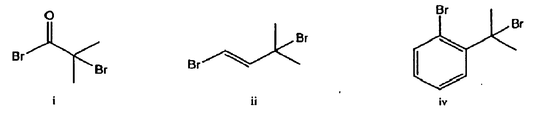
- Among them, the compound (i) is preferable because it is easier to handle and allows efficient initiation of polymerization. In this manner, the compounds (c) and (f) (those expressed by the general formula (1)) are preferably used as polymerization initiators.
- An amount of the Z1Q to be used ranges preferably from 2 to 5 equivalent with respect to each of the compounds (b) and (f), and more preferably from 2 to 3 equivalent with respect thereto. In this manner, the polymerization initiating groups can be adequately introduced.
- The reaction solvents and bases are the same as those described in the above step A1. In the synthesis of the nonsymmetrical disulfide compound, sodium hydroxide is a preferable base. In addition, an amount thereof to be used is in a range preferably from 2 to 4, and more preferably 2.5 to 3. In this manner, the nonsymmetrical disulfide compound can be efficiently synthesized.
- The reaction temperature varies with reaction substrates, Z1Q, reaction solvents and the kinds of the bases. The temperature is preferably from 5 degrees centigrade below zero to 5 degrees centigrade, and more preferably from 2 degrees below zero to 2 degrees centigrade.
- The reaction time varies with reaction substrates, Z1Q, reaction solvents and the kinds of the bases. It is only necessary that the time ranges from 3 to 8 hours and more preferably from 5 to 6 hours.
- Thus, in the manner as described above, there can be obtained the compounds (c) and (g) (those expressed by the general formula (1)) in which the polymerization initiating group Z1 has been introduced to Y1 of each of the compounds (b) and (f).
- The compounds (c) and (g) obtained as above have a covalent bond (according to an Au-S bond) with a metal substrate, for example, with a surface of a gold thin film via disulfide. Then, living polymerization is promoted by the polymerization initiating group formed at a molecular end, so that a polymer film is formed on the metal substrate.
- Additionally, in the above A1 step, if CH2COCl is used to appropriately determine a reaction reagent, a compound can be synthesized in which the S of each of the compounds (a) and (d) has been protected by an acetyl group.
- Polymerization Initiator
The compound according to the embodiment, as is obtained above, includes the polymerization initiating group. Thus, the compound can be used by being contained in a polymerization initiator. For example, such a polymerization initiator may contain the compound within a range of 10 to 100 percent by weight and preferably 50 to 100 percent by weight. - The polymerization initiator may also contain various additives such a plasticizer, an antistatic agent and a coloring agent.
- Furthermore, since the compound according to the embodiment has the SX group, it can be bonded to a substrate having a metal thereon to be used for an electronic device substrate. In this case, the compound according to the embodiment, which is bonded to the metal of the substrate surface, can be used as an underlying layer. Then, the polymerization initiating group performs graft polymerization, living polymerization, block polymerization or the like of various physiologically active substances and functionalized substances. Accordingly, such an electronic device substrate using the compound can be advantageous for various kinds of sensors including an ion sensor and an organic sensor.
- Electronic Device Substrate
Hereinafter, a detailed description will be given of an electronic device substrate according to embodiments of the invention by referring to the drawings. - Fig. 1 is a schematic sectional view of an electronic device substrate 1 according to an embodiment of the invention. In the description below, upper and lower sides in Fig. 1 mean "upper" and "lower" sides, respectively. Additionally, the same parts as those in the description of the compound will not be described below.
- The electronic device substrate 1 shown in Fig. 1 includes a
substrate 2 and an underlying layer 3 in which the compound expressed by the general formula (1) has been bonded to asurface 21 of thesubstrate 2 via a sulfur atom. - The structure of each part will now be sequentially explained below.
- The
substrate 2 supports the underlying layer 3 and/or supplies electricity to a device. In addition, thesubstrate 2 is configured to have at least one of a metal and a metal oxide on thesurface 21 thereof. Then, the at least one of the metal and the metal oxide is bonded to the compound expressed by the general formula (1) via the sulfur atom, so that the underlying layer 3 is laminated on thesurface 21 thereof. - Materials of the
substrate 2 may be, for example, any one of various kinds of glasses, quartz, silicon, metals such as molybdenum sulfide, copper, zinc, aluminum, stainless steel, magnesium, iron, nickel, gold, silver and platinum, transparent conductive metal oxides such as indium-tin oxide (ITO), indium-zinc oxide (IZO), aluminum-zinc oxide (AZO) and gallium-zinc oxide (GZO), semiconductors such as gallium arsenide and various kinds of plastics. - Among them, metals or metal oxides bondable to the compound expressed by the general formula (1) are preferred. As more bondable materials, gold, silver, platinum, gallium arsenide are more preferable. Particularly, gold is the most preferable because of its firm and stable bonding properties. In this manner, any one of them (particularly gold) can be covalently bonded to the compound expressed by the general formula (1). As a result, the electronic device substrate 1 can include the compound of the general formula (1) that has been stably bonded to the
surface 21 of thesubstrate 2. - When the
substrate 2 is made of a material other than a metal and a metal oxide, it is preferable to have at least one of a metal and a metal oxide on thesurface 21 thereof. In this manner, the compound of the general formula (1) can be bonded to the at least one of them thereon via the sulfur atom. - In this case, the metal on the
surface 21 of thesubstrate 2 is not specifically limited as long as it can be bonded to the sulfur atom. For example, the metal may be gold, silver, platinum, gallium arsenide or the like. Among them, gold is particularly preferable because it can be firmly bonded to the sulfur atom. In this manner, gold has a covalent bond with the compound of the general formula (1). Therefore, in the electronic device substrate 1 obtained, the compound of the general formula (1) has been firmly and stably bonded to thesurface 21 thereof. - Examples of the metal oxide formed on the
surface 21 thereof may include transparent conductive oxides such as ITO, IZO, AZO and GZO. - It is only necessary that the
substrate 2 has at least one of such a metal and a metal oxide on thesurface 21 thereof. Alternatively, both of them may be formed thereon. In order to easily obtain thesubstrate 2, it is preferable to form one of them on thesurface 21, and particularly preferable to have a metal that is easily bondable to the compound of the general formula (1). - The material of the
substrate 2 may be a combination of two or more kinds of materials. For example, there may be mentioned a combination of a metal and a metal oxide, a combination of a metal and silicon, a combination of a glass and silicon or the like. Additionally, the metal and the metal oxide disposed on thesurface 21 thereof may be a combination of two or more different kinds of them. - A mean thickness of the
substrate 2 is not specifically limited. In a case of thesubstrate 2 made of a metal, a preferable mean thickness thereof ranges approximately from 50 to 200 nm and more preferably approximately from 100 to 150 nm. - When the
substrate 2 is made of a material other than metals, the mean thickness thereof preferably ranges approximately from 0.1 to 2,000 nm, and more preferably approximately from 1 to 1,000 nm. - The underlying layer 3 has the compound expressed by the general formula (1). Additionally, the underlying layer 3 is a layer that has been bonded to the at least one of the metal and the metal oxide on the
surface 21 thereof via the sulfur atom of the compound. Furthermore, the underlying layer 3 allows bonding, polymerization and lamination of various compounds through the polymerization initiating group Z1 of the compound of the general formula (1). - In the present embodiment, the underlying layer 3 is comprised of only the compound expressed by the general formula (1). However, the layer may also include any other compound as long as it contains the compound of the general formula (1). An amount of the compound of the general formula (1) to be included is preferably equivalent to an amount including it as a main material. More preferably, the amount thereof to be included ranges from 50 to 100 percent by weight and most preferably from 70 to 100 percent by weight. In this manner, the underlying layer 3 can sufficiently include the compound of the general formula (i), so that electrons can be adequately moved.
- A mean thickness of the underlying layer 3 varies with a degree of polymerization m1 in the compound expressed by the general formula (1). A preferable mean thickness thereof ranges from 0.5 to 5 nm and more preferably from 1 to 3 nm. In this manner, electrons can be adequately moved.
- The underlying layer 3 is preferably configured so as to include a group having the following structure:
-

- In the above structural formula, m1 is an integer from 1 to 15. In this manner, the electronic device substrate 1 can be easily obtained in which the underlying layer 3 has been firmly and stably bonded to the
surface 21 of thesubstrate 2. Additionally, since -O-(CH2)2- is used as a spacer, electrons can be more adequately moved (ion penetration). - With the structure as described above, there can be produced the electronic device substrate 1 according to the embodiment. In the electronic device substrate 1, living polymerization is promoted by the polymerization initiator located at the molecular end to form a polymer film. Thus, the electronic device substrate 1 is preferably used as a substrate for an ion sensor, an organic sensor, a biosensor or the like, for example.
- Method for Manufacturing the Electronic Device Substrate
- Next, a description will be given as to an example of a method for manufacturing the electronic device substrate 1 described above. The same parts as those in the above description will be omitted below.
- The electronic device substrate 1 according to the embodiment can be produced, for example, by contacting the
substrate 2 having at least one of a metal and a metal oxide on thesurface 21 thereof with the underlying layer 3 comprised of a compound expressed by the following general formula (1) to form a metal-sulfur bond on thesurface 21 thereof. -

- In the above formula, X represents one of a hydrogen atom and a protecting group ; Y1 represents one of an oxygen atom, an alkylene group and - N(R1)-, in which R1 represents an alkyl group; Z1 represents a polymerization initiating group; n1 represents an integer from 1 to 4 ; and m1 represents an integer from 1 to 15.
- When the
substrate 2 is made of a material other than the metal and the metal oxide, it is preferable to provide at least one of the metal and the metal oxide on thesurface 21. In this case, any one of known methods may be used. For example, there may be used vacuum coating such as sputtering, chemical vapor deposition (CVD) such as plasma CVD, thermal CVD or laser CVD, a dry process such as vacuum evaporation or ion plating, a wet process such as electrolyte plating, immersion plating or electroless plating, a spray process, a sol-gel process, a metal organic decomposition (MOD) process, bonding of a sheet material or the like. - The compound expressed by the general formula (1) may be contacted with the
substrate 2 in a manner as follows. For example, thesubstrate 2 having the at least one of the metal and the metal oxide on thesurface 21 thereof will be immersed in a 1-mmol ethanol solution of the compound of the general formula (1) for 1 hour under a room temperature (25 degrees centigrade). Alternatively, spin coating, dip coating, an inkjet method or the like may be used. - Regarding concrete conditions for the contact, a preferable temperature ranges from 10 to 40 degrees centigrade and a preferable time ranges from 1 to 24 hours. More preferably, the temperature and time, respectively, range from 15 to 30 degrees centigrade and 1 to 12 hours, respectively. Under those conditions, the compound of the general formula (1) can be adequately bonded to the
surface 21 thereof, so that the underlying layer 3 can be easily formed. - Additionally, the X may be a group expressed by the following formula:
-

- In the above formula, Y2 represents one of an oxygen atom, an alkylene group and -N(R2)-, in which R2 represents an alkyl group; Z2 represents a polymerization initiating group; n2 represents an integer from 1 to 4; and m2 represents an integer from 1 to 15. In that case, as shown in Fig. 2, while maintaining a formed S-S bond, the sulfur atom and the at least one of the metal and the metal oxide have a covalent bond (according to the Au-S bond) with each other. In this situation, due to steric hindrance, the compound of the general formula (1) is not closely bonded to the
surface 21 of thesubstrate 2. Thus, the S-S bond will be separated as time passes and the compound structure will change into an upright structure on thesubstrate 2, as shown in Fig 1. In this manner, without deprotection of the X in the compound of the general formula (1), the compound thereof (1) can be bonded upright to thesubstrate 2. Accordingly, the electronic device substrate 1 having high ionic permeability can be easily obtained. - With the method as described above, there can be obtained the electronic device substrate 1 according to the embodiment.
- 1. Manufacturing of the Compound expressed by the General Formula (1).
-

- In a round bottom flask, 5g of polyethylene glycol thiol (a) having a degree of polymerization (n) of 7 was dissolved in 100 mL of dichloromethane and the obtained solution was mixed with 40 mL of 10% aqueous solution of potassium hydrogen carbonate. Then, the mixture solution was stirred (two-layered state) at a room temperature. After dissolving 2.0 g of bromine in 2 mL of ethanol, the solution was added to the mixture solution under stirring. The obtained solution was kept stirring for approximately 1 hour at a room temperature. A brown bromine component was immediately added for reaction and turned to be colorless. Thereafter, a reaction mixture was extracted with dichloromethane to collect a dichloromethane organic layer. After drying the layer with magnesium sulfate, an obtained filtrate was condensed by a low-pressure evaporator to obtain the compound (b) with a yield of 85%. The measurement of a mass spectrometry (MS) spectrum of the obtained compound (b) showed that the compound (b) has a molecular weight of 742.
- Next, after dissolving the obtained compound (b) in 100 ml of dichloromethane, the solution was mixed with 40 mL of a 10 aqueous solution of triethylamine and stirred (two-layered state) at a room temperature. Next, 2g of 2-bromo-2-methyl-ethylbromoketone was dissolved in 2 mL of ethanol and the solution was added to the mixture solution under stirring. The obtained solution was kept stirring for approximately 1 hour at a room temperature. Thereafter, a reaction mixture was extracted with dichloromethane to collect a dichloromethane organic layer. After drying the layer with magnesium sulfate, an obtained filtrate was condensed by the low-pressure evaporator to obtain the compound (c) with a yield of 85%. In the measurement of an MS spectrum of the obtained compound (c), the compound (c) was identified to have a molecular weight of 1040.
- Example 2 was performed in the same manner as Example 1, except that polyethylene glycol thiol having a degree of polymerization (n) of 3 was used instead of that having the degree of polymerization (n) of 7 in Example 1. Then, with the same yield, a symmetrical disulfide compound was obtained that has a polymerization initiating group having a molecular weight of 688.
- Example 3 was performed in the same manner as Example 1, except that polyethylene glycol thiol having a degree of polymerization (n) of 11 was used instead of that having the degree of polymerization (n) of 7 in Example 1. Then, with the same yield, a symmetrical disulfide compound was obtained that has a polymerization initiating group having a molecular weight of 1392.
- Example 4 was performed in the same manner as Example 1, except that 1, 3-dibromo-3-methyl-1-butene was used instead of the 2-bromo-2-methyl-ethylbromoketone in Example 1. Then, with the same yield, a symmetrical disulfide compound was obtained that has a polymerization initiating group having a molecular weight of 1036.
- Example 5 was performed in the same manner as Example 1, except that 1-bromo-2-(2'-bromo-2'-methyl)-ethyl-benzene was used instead of the 2-bromo-2-methyl-ethylbromoketone in Example 1. Then, with the same yield, a symmetrical disulfide compound was obtained that has a polymerization initiating group having a molecular weight of 1136.
- 2. Manufacturing of the Electronic Device Substrate
- A gold substrate having a thickness of 100 nm was immersed in a 1-mmol of ethanol solution containing the compound obtained in Example 1 for 1 hour at a room temperature (25 degrees centigrade). Then, ethanol washing and nitrogen drying were performed to obtain an electronic device substrate. In a measurement by the Fourier Transform Infrared (FT-IR) Spectrometer (thermo Nexsus 870 by Nicore Japan Co.), peak positions of functional groups (-O-, -S-, - C=O, etc.) of the compound obtained in Example 1 were observed and thereby bonding of the compound to the substrate surface was confirmed.
- Example 7 was performed in the same manner as Example 6 to obtain an electronic device substrate, except that the compound obtained in Example 2 was used instead of the compound obtained in Example 1.
- Example 8 was performed in the same manner as Example 6 to obtain an electronic device substrate, except that the compound obtained in Example 3 was used instead of the compound obtained in Example 1.
- Example 9 was performed in the same manner as Example 6 to obtain an electronic device substrate, except that the compound obtained in Example 4 was used instead of the compound obtained in Example 1.
- Example 10 was performed in the same manner as Example 6 to obtain an electronic device substrate, except that the compound obtained in Example 5 was used instead of the compound obtained in Example 1.
- Example 11 was performed in the same manner as Example 6 to obtain an electronic device substrate, except that a silicon substrate having a thickness of 100 nm and having ITO formed on a surface thereof was used instead of the gold substrate having the same thickness.
- Comparative example 1 was performed in the same manner as Example 6 to obtain an electronic device substrate, except that a compound (h) having the following structure was used instead of the compound obtained in Example 1.
-

- Comparative example 2 was performed in the same manner as Example 6 to obtain an electronic device substrate, except that a compound (i) having the following structure was used instead of the compound obtained in Example 1.
-

- Although the present invention has been described in detail, it will be apparent to those skilled in the art that the invention may be embodied in a variety of specific forms and that various changes, substitutions and alterations can be made without departing from the spirit and scope of the invention. The described embodiments and examples are only illustrative and not restrictive. The scope of the invention is, therefore, indicated by the following claims.
Claims (12)
- An electronic device substrate, comprising:a substrate having at least one of a metal and a metal oxide on a surface thereof, andan underlying layer having a compound expressed by a following general formula (1) :wherein X represents one of a hydrogen atom and a protecting group; Y1 represents one of an oxygen atom, a C1-C20 alkylene group and -N(R1)-, in which R1 represents a C1-C20 alkyl group; Z1 represents a polymerization initiating group; n1 represents an integer from 1 to 4 ; and m1 represents an integer from 1 to 15.

- The electronic device substrate according to Claim 1, wherein the compound expressed by the general formula (1) is bonded to the at least one of the metal and the metal oxide via a sulfur atom.
- The electronic device substrate according to Claim 1, wherein the metal is one of gold, silver and platinum.
- The electronic device substrate according to Claim 1, wherein the metal oxide is a transparent conductive metal oxide.
- The electronic device substrate according to Claim 1, the polymerization initiating group Z1 of the compound expressed by the general formula (1) has one of following structures (I), (II) and (III):


- The electronic device substrate according to Claim 1, wherein the n1 of the compound expressed by the general formula (1) is 2.
- A method for manufacturing an electronic device substrate, comprising contacting a compound expressed by a following general formula (1) with a substrate having at least one of a metal and a metal oxide on a surface thereof to form a metal-sulfur bond on the surface thereof, the general formula (1) being as follows :

- The method for manufacturing an electronic device substrate according to Claim 7, wherein the protecting group X of the compound expressed by the general formula (1) is expressed by a following formula:

- A compound expressed by a following general formula (1) :
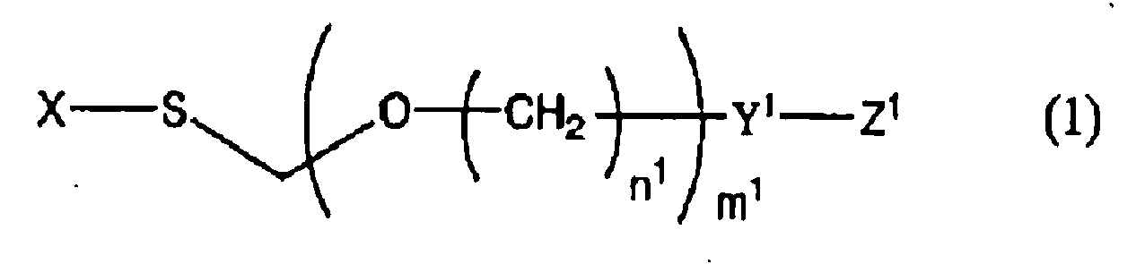
- The compound according to Claim 9, wherein the n1 of the compound expressed by the general formula (1) is 2; the m1 thereof is one of 3, 7 and 11; and the polymerization initiating group Z1 thereof has a following structure:

- A method for manufacturing the compound according to Claim 9, comprising reacting, in the presence of a base, a compound expressed by a following general formula (2) with a compound expressed by a following formula (3), the general formula (2) being as follows:

Z1-Q (3)
wherein Z1 represents a polymerization initiating group and Q represents a halogen atom. - A polymerization initiator comprising the compound according to Claim 9.
Applications Claiming Priority (1)
| Application Number | Priority Date | Filing Date | Title |
|---|---|---|---|
| JP2006129311A JP4175380B2 (en) | 2006-05-08 | 2006-05-08 | SUBSTRATE FOR ELECTRONIC DEVICE, PROCESS FOR PRODUCING THE SAME, COMPOUND USED FOR THEM, PROCESS FOR PRODUCING THE COMPOUND AND POLYMERIZATION INITIATOR CONTAINING COMPOUND USED FOR SUBSTRATE FOR ELECTRONIC DEVICE |
Publications (2)
| Publication Number | Publication Date |
|---|---|
| EP1854553A1 true EP1854553A1 (en) | 2007-11-14 |
| EP1854553B1 EP1854553B1 (en) | 2014-11-05 |
Family
ID=38335698
Family Applications (1)
| Application Number | Title | Priority Date | Filing Date |
|---|---|---|---|
| EP20070251888 Ceased EP1854553B1 (en) | 2006-05-08 | 2007-05-04 | Electronic device substrate, method for manufacturing substrate |
Country Status (4)
| Country | Link |
|---|---|
| US (1) | US7955705B2 (en) |
| EP (1) | EP1854553B1 (en) |
| JP (1) | JP4175380B2 (en) |
| CN (1) | CN101071118B (en) |
Cited By (1)
| Publication number | Priority date | Publication date | Assignee | Title |
|---|---|---|---|---|
| EP3604386A4 (en) * | 2017-03-30 | 2020-10-28 | NOF Corporation | DEGRADABLE POLYETHYLENE GLYCOL DERIVATIVE WITH DISULFIDE LINKER |
Families Citing this family (1)
| Publication number | Priority date | Publication date | Assignee | Title |
|---|---|---|---|---|
| US9456780B2 (en) * | 2013-02-07 | 2016-10-04 | Hill-Rom Services, Inc. | Dynamic therapy delivery system |
Family Cites Families (6)
| Publication number | Priority date | Publication date | Assignee | Title |
|---|---|---|---|---|
| JPH0777509A (en) | 1993-06-30 | 1995-03-20 | New Oji Paper Co Ltd | Electrochemical measurement electrode |
| US7807348B2 (en) * | 2002-03-20 | 2010-10-05 | Wisconsin Alumni Research Foundation | Optical imaging of nanostructured substrates |
| GB2413553A (en) * | 2004-04-29 | 2005-11-02 | Seiko Epson Corp | UV decomposable molecules and a photopatternable monomolecular film formed therefrom |
| JP2006242926A (en) | 2005-03-07 | 2006-09-14 | Seiko Epson Corp | Electrode substrate, detection device including the substrate, kit including the device, and detection method using the kit |
| JP2006242925A (en) | 2005-03-07 | 2006-09-14 | Seiko Epson Corp | Electrode substrate, detection device including the substrate, kit including the device, and detection method using the kit |
| JP2006261240A (en) * | 2005-03-15 | 2006-09-28 | Seiko Epson Corp | Electronic device substrate, method for manufacturing electronic device substrate, display device, and electronic apparatus |
-
2006
- 2006-05-08 JP JP2006129311A patent/JP4175380B2/en not_active Expired - Fee Related
-
2007
- 2007-04-25 US US11/739,837 patent/US7955705B2/en not_active Expired - Fee Related
- 2007-04-27 CN CN200710101919XA patent/CN101071118B/en not_active Expired - Fee Related
- 2007-05-04 EP EP20070251888 patent/EP1854553B1/en not_active Ceased
Non-Patent Citations (5)
| Title |
|---|
| LI DEJIN ET AL: "Thermosensitive hairy hybrid nanoparticles synthesized by surface-initiated atom transfer radical polymerization.", LANGMUIR : THE ACS JOURNAL OF SURFACES AND COLLOIDS 28 MAR 2006, vol. 22, no. 7, 28 March 2006 (2006-03-28), pages 3344 - 3351, XP002447096, ISSN: 0743-7463 * |
| PLUNKETT KYLE N ET AL: "PNIPAM chain collapse depends on the molecular weight and grafting density", LANGMUIR; LANGMUIR APR 25 2006, vol. 22, no. 9, 25 April 2006 (2006-04-25), pages 4259 - 4266, XP002447095 * |
| XU CHANG ET AL: "MicroChannel confined surface-initiated polymerization", MACROMOLECULES; MACROMOLECULES JAN 11 2005, vol. 38, no. 1, 11 January 2005 (2005-01-11), pages 6 - 8, XP002447097 * |
| XU D ET AL: "Functionalization of hydrogen-terminated silicon via surface-initiated atom-transfer radical polymerization and derivatization of the polymer brushes", JOURNAL OF COLLOID AND INTERFACE SCIENCE, ACADEMIC PRESS, NEW YORK, NY, US, vol. 279, no. 1, 1 November 2004 (2004-11-01), pages 78 - 87, XP004562973, ISSN: 0021-9797 * |
| XU F J ET AL: "UV-induced coupling of 4-vinylbenzyl chloride on hydrogen-terminated Si(100) surfaces for the preparation of well-defined polymer-Si hybrids via surface-initiated ATRP", MACROMOLECULES; MACROMOLECULES MAR 8 2005, vol. 38, no. 5, 8 March 2005 (2005-03-08), pages 1573 - 1580, XP002447098 * |
Cited By (2)
| Publication number | Priority date | Publication date | Assignee | Title |
|---|---|---|---|---|
| EP3604386A4 (en) * | 2017-03-30 | 2020-10-28 | NOF Corporation | DEGRADABLE POLYETHYLENE GLYCOL DERIVATIVE WITH DISULFIDE LINKER |
| US11220576B2 (en) | 2017-03-30 | 2022-01-11 | Nof Corporation | Degradable polyethylene glycol derivative having disulfide linker |
Also Published As
| Publication number | Publication date |
|---|---|
| CN101071118A (en) | 2007-11-14 |
| JP2007303832A (en) | 2007-11-22 |
| US20070259187A1 (en) | 2007-11-08 |
| CN101071118B (en) | 2013-01-02 |
| EP1854553B1 (en) | 2014-11-05 |
| JP4175380B2 (en) | 2008-11-05 |
| US7955705B2 (en) | 2011-06-07 |
Similar Documents
| Publication | Publication Date | Title |
|---|---|---|
| AU2002252868C1 (en) | Detection of negatively charged polymers using water-soluble, cationic, polythiophene derivatives | |
| KR102240669B1 (en) | Organic electrochemical transistor device and method for preparing the same | |
| Ponnappa et al. | Naphthalene flanked diketopyrrolopyrrole: a new conjugated building block with hexyl or octyl alkyl side chains for electropolymerization studies and its biosensor applications | |
| KR20130114096A (en) | Substituted 3,4-propylenedioxythiophene monomers and 3,4- propylenedioxythiophene-based crosslinkers and polymers thereof | |
| US12504396B2 (en) | Polycyclic aromatic bridges for molecular electronic sensors | |
| EP1854553B1 (en) | Electronic device substrate, method for manufacturing substrate | |
| Balog et al. | A versatile building block for EDOT or PEDOT functionalization | |
| Lu et al. | Synthesis, characterization, and vitamin C detection of a novel L-alanine-modified PEDOT with enhanced chirality | |
| JP2003335846A (en) | Novel conductive polymer, sensor and target substance detection method using the same | |
| CN101801985A (en) | redox mediators | |
| CN104311465A (en) | ω-vinylsulfone-based disulfide compound, its preparation method and application | |
| US20100126880A1 (en) | Dna complexing agents | |
| JP2012049287A (en) | Surface modification silicon substrate | |
| US9056872B2 (en) | Organic compounds, process for preparing same and uses in electronics | |
| CN100436472C (en) | Substituted pyrroles with oligonucleotides | |
| US11739179B2 (en) | Disulfide-containing monomer, its reduced form, and its derivate, method to synthesize the same, and polymer containing the same | |
| WO2007133714A2 (en) | Analyte focusing biochips for affinity mass spectrometry | |
| Li et al. | Conducting polythiophenes with a broad spectrum of reactive groups | |
| JP2004269532A (en) | Conductive compound, electrode and sensor containing the same, and method for detecting target molecule using the sensor | |
| Colleran et al. | Non-trivial solution chemistry between amido-pyridylcalix [4] arenes and some metal salts | |
| KR100601999B1 (en) | Target material detection method using novel conductive polymer | |
| US7833406B2 (en) | Gene detection method, and intercalator | |
| Oberoi et al. | Novel modified pyrrole monomers, 1: Synthesis and characterization | |
| Ticha et al. | Self-Assembled Monolayer of Cyclopentadienyl Ruthenium Thiolate Schiff Base-on-Gold, for Amperometric Detection of H2O2 | |
| JP4303707B2 (en) | Chemical modification immobilization method of polythiophene derivatives on metal surface |
Legal Events
| Date | Code | Title | Description |
|---|---|---|---|
| PUAI | Public reference made under article 153(3) epc to a published international application that has entered the european phase |
Free format text: ORIGINAL CODE: 0009012 |
|
| AK | Designated contracting states |
Kind code of ref document: A1 Designated state(s): AT BE BG CH CY CZ DE DK EE ES FI FR GB GR HU IE IS IT LI LT LU LV MC MT NL PL PT RO SE SI SK TR |
|
| AX | Request for extension of the european patent |
Extension state: AL BA HR MK YU |
|
| 17P | Request for examination filed |
Effective date: 20080311 |
|
| AKX | Designation fees paid |
Designated state(s): DE FR GB |
|
| 17Q | First examination report despatched |
Effective date: 20100504 |
|
| RIC1 | Information provided on ipc code assigned before grant |
Ipc: H01L 51/05 20060101ALI20140403BHEP Ipc: B05D 7/02 20060101AFI20140403BHEP Ipc: C08J 7/18 20060101ALI20140403BHEP Ipc: H01L 51/00 20060101ALI20140403BHEP Ipc: C08F 293/00 20060101ALI20140403BHEP Ipc: C08F 290/14 20060101ALI20140403BHEP Ipc: C08F 291/00 20060101ALI20140403BHEP Ipc: B82Y 10/00 20110101ALI20140403BHEP Ipc: C08F 292/00 20060101ALI20140403BHEP |
|
| GRAP | Despatch of communication of intention to grant a patent |
Free format text: ORIGINAL CODE: EPIDOSNIGR1 |
|
| INTG | Intention to grant announced |
Effective date: 20140521 |
|
| RIN1 | Information on inventor provided before grant (corrected) |
Inventor name: FUKUSHIMA, HITOSHI Inventor name: YOKOKAWA, SHINOBU |
|
| GRAS | Grant fee paid |
Free format text: ORIGINAL CODE: EPIDOSNIGR3 |
|
| GRAA | (expected) grant |
Free format text: ORIGINAL CODE: 0009210 |
|
| AK | Designated contracting states |
Kind code of ref document: B1 Designated state(s): DE FR GB |
|
| REG | Reference to a national code |
Ref country code: GB Ref legal event code: FG4D |
|
| REG | Reference to a national code |
Ref country code: DE Ref legal event code: R096 Ref document number: 602007039117 Country of ref document: DE Effective date: 20141218 |
|
| REG | Reference to a national code |
Ref country code: DE Ref legal event code: R097 Ref document number: 602007039117 Country of ref document: DE |
|
| PLBE | No opposition filed within time limit |
Free format text: ORIGINAL CODE: 0009261 |
|
| STAA | Information on the status of an ep patent application or granted ep patent |
Free format text: STATUS: NO OPPOSITION FILED WITHIN TIME LIMIT |
|
| 26N | No opposition filed |
Effective date: 20150806 |
|
| REG | Reference to a national code |
Ref country code: FR Ref legal event code: PLFP Year of fee payment: 10 |
|
| REG | Reference to a national code |
Ref country code: FR Ref legal event code: PLFP Year of fee payment: 11 |
|
| REG | Reference to a national code |
Ref country code: FR Ref legal event code: PLFP Year of fee payment: 12 |
|
| PGFP | Annual fee paid to national office [announced via postgrant information from national office to epo] |
Ref country code: DE Payment date: 20200422 Year of fee payment: 14 Ref country code: FR Payment date: 20200414 Year of fee payment: 14 |
|
| PGFP | Annual fee paid to national office [announced via postgrant information from national office to epo] |
Ref country code: GB Payment date: 20200422 Year of fee payment: 14 |
|
| REG | Reference to a national code |
Ref country code: DE Ref legal event code: R119 Ref document number: 602007039117 Country of ref document: DE |
|
| GBPC | Gb: european patent ceased through non-payment of renewal fee |
Effective date: 20210504 |
|
| PG25 | Lapsed in a contracting state [announced via postgrant information from national office to epo] |
Ref country code: GB Free format text: LAPSE BECAUSE OF NON-PAYMENT OF DUE FEES Effective date: 20210504 Ref country code: DE Free format text: LAPSE BECAUSE OF NON-PAYMENT OF DUE FEES Effective date: 20211201 |
|
| PG25 | Lapsed in a contracting state [announced via postgrant information from national office to epo] |
Ref country code: FR Free format text: LAPSE BECAUSE OF NON-PAYMENT OF DUE FEES Effective date: 20210531 |