EP1848169B1 - Frequency offset estimator - Google Patents
Frequency offset estimator Download PDFInfo
- Publication number
- EP1848169B1 EP1848169B1 EP07075540.0A EP07075540A EP1848169B1 EP 1848169 B1 EP1848169 B1 EP 1848169B1 EP 07075540 A EP07075540 A EP 07075540A EP 1848169 B1 EP1848169 B1 EP 1848169B1
- Authority
- EP
- European Patent Office
- Prior art keywords
- detector
- frequency offset
- magnitude
- clockwise
- zero
- Prior art date
- Legal status (The legal status is an assumption and is not a legal conclusion. Google has not performed a legal analysis and makes no representation as to the accuracy of the status listed.)
- Expired - Lifetime
Links
Images


Classifications
-
- H—ELECTRICITY
- H04—ELECTRIC COMMUNICATION TECHNIQUE
- H04L—TRANSMISSION OF DIGITAL INFORMATION, e.g. TELEGRAPHIC COMMUNICATION
- H04L27/00—Modulated-carrier systems
- H04L27/18—Phase-modulated carrier systems, i.e. using phase-shift keying
- H04L27/22—Demodulator circuits; Receiver circuits
- H04L27/233—Demodulator circuits; Receiver circuits using non-coherent demodulation
- H04L27/2332—Demodulator circuits; Receiver circuits using non-coherent demodulation using a non-coherent carrier
-
- H—ELECTRICITY
- H04—ELECTRIC COMMUNICATION TECHNIQUE
- H04L—TRANSMISSION OF DIGITAL INFORMATION, e.g. TELEGRAPHIC COMMUNICATION
- H04L27/00—Modulated-carrier systems
- H04L27/18—Phase-modulated carrier systems, i.e. using phase-shift keying
- H04L27/22—Demodulator circuits; Receiver circuits
- H04L27/227—Demodulator circuits; Receiver circuits using coherent demodulation
- H04L27/2275—Demodulator circuits; Receiver circuits using coherent demodulation wherein the carrier recovery circuit uses the received modulated signals
-
- H—ELECTRICITY
- H04—ELECTRIC COMMUNICATION TECHNIQUE
- H04L—TRANSMISSION OF DIGITAL INFORMATION, e.g. TELEGRAPHIC COMMUNICATION
- H04L27/00—Modulated-carrier systems
- H04L27/0014—Carrier regulation
- H04L2027/0044—Control loops for carrier regulation
- H04L2027/0063—Elements of loops
- H04L2027/0065—Frequency error detectors
-
- H—ELECTRICITY
- H04—ELECTRIC COMMUNICATION TECHNIQUE
- H04L—TRANSMISSION OF DIGITAL INFORMATION, e.g. TELEGRAPHIC COMMUNICATION
- H04L27/00—Modulated-carrier systems
- H04L27/0014—Carrier regulation
- H04L2027/0083—Signalling arrangements
- H04L2027/0087—Out-of-band signals, (e.g. pilots)
Definitions
- the present invention relates to radio receivers and, in particular, to a system and method for frequency offset estimation.
- a carrier frequency is generated by a local oscillator and is modulated by a baseband signal. More specifically, two sinusoidal carriers of the same frequency, but having a ninety-degree phase offset, are modulated by the real (I) and imaginary (Q) parts of a complex valued baseband signal.
- coherent demodulation requires exactly the same carrier frequency and phase.
- a frequency offset error appears in the demodulated baseband signal for one reason, or a combination of several reasons.
- the local oscillator frequency used in the receiver generally may not exactly match the frequency used by the local oscillator transmitter.
- the received signal may be affected by a Doppler spread.
- the demodulated in-phase and quadrature components (I' and Q') of the baseband signal differ from the transmitted components (I and Q) by a variable phase offset. This results in a steady rotation of the whole I-Q constellation diagram which can adversely impact the accuracy of baseband signal reception and detection.
- a predefined word (often referred to as a pilot) signal provides a reference that can be used for frequency offset measurement. Once the offset is measured, the local oscillator at the receiver can be tuned to correct for that offset.
- the document US 5 779 043 shows a method of compensating for a frequency error in a frequency shift keying receiver.
- the present invention is directed to a computationally efficient system and method for measurement of frequency offset error. More specifically, the present invention utilizes measurements made on a demodulated signal (for example, a pilot signal) to determine both a direction and magnitude of the frequency offset.
- a demodulated signal for example, a pilot signal
- the present invention provides a frequency offset detector as claimed in claim 1, and a method of detecting a frequency offset as claimed in claim 15.
- a frequency offset sign and magnitude of a received complex signal is measured by detecting at least one quadrant transition of the received complex signal in both a counter-clockwise and clockwise rotation direction. The detected transitions are separately accumulated over a time period. By comparing the accumulated counter-clockwise and clockwise quadrant transitions, a difference value is obtained. The sign of that difference value provides the frequency offset sign, and the magnitude of that difference value provides information indicative of the frequency offset magnitude.
- a frequency offset sign and magnitude of a received complex signal is measured by detecting at least one quadrant transition of the received complex signal in both a counter-clockwise and clockwise rotation direction as well as at least one zero-crossing transition.
- the detected transitions are separately accumulated over a time period.
- information indicative of frequency offset sign may be obtained.
- the accumulated zero-crossing transitions provides information indicative of the frequency offset magnitude.
- a frequency offset sign and magnitude of a received complex signal is measured by detecting at least one quadrant transition of the received complex signal in both a counter-clockwise and clockwise rotation direction as well as at least one zero-crossing transition.
- the detected transitions are separately accumulated over a time period.
- a difference value is obtained.
- the sign of that difference value provides the frequency offset sign.
- the magnitude of that difference value is then compared to a threshold. If the threshold is exceeded, the accumulated zero-crossing transitions provides information indicative of the frequency offset magnitude. However, if the threshold is not exceeded, the magnitude of that difference value provides information indicative of the frequency offset magnitude.
- the frequency offset detectors in accordance with the present invention may be used in a number of applications. More specifically, the frequency offset sign and magnitude information is useful in adjusting a local operator frequency in order to improve receiver performance.
- the frequency offset magnitude and sign information may be generated in a UMTS-FDD cell searcher step 3 functionality by processing the received complex pilot channel signal, with the output magnitude and sign information used to adjust the local oscillator frequency for the UMTS-FDD receiver.
- pilot sequence symbols used are all identical.
- each of the pilot QPSK components carry all ones, and hence Ae j ⁇ (k) can be expressed as: 2 e j ⁇ / 4
- the QPSK components contain a phase error that is, in the case of a frequency error ⁇ 1 - ⁇ , variable and amounts to ( ⁇ 1 - ⁇ ) t + ⁇ .
- the received phase components I' and Q' contain variable mixtures of original QPSK components I and Q
- the frequency offset estimation comprises the finding the ( ⁇ 1 - ⁇ ) term.
- a frequency offset causes the above-referenced phase components I'(k) and Q'(k) to fluctuate as sine waves.
- Each 0 to 2n cycle can be characterized by a characteristic event.
- the characteristic event is a simultaneous appearance of a zero crossing on one component (for example, I'(k)) and of an extremum on the other component (for example, Q'(k)), as shown in FIGURE 1 .
- the characteristic event is a zero crossing on one (or both) component (s).
- the extremum can be assumed to be detected on one component when both (1) the sign of this component does not change, and (2) a zero crossing is detected on the other component. It is thus recognized that both events (1) and (2) can be tracked simply from detection of possible sign changes. Additionally, for purposes of the frequency offset detection operation, the I' (k) and Q' (k) components can be quantized with only one bit (i.e., the sign bit). The one bit and sign change characteristics lead to several efficient designs for offset detection and measurement.
- FIGURE 2 wherein there is shown a diagram synthetically illustrating one bit event counting.
- the arrows 10 pointing in a counterclockwise direction correspond to a sequence of events caused by a positive frequency offset
- the arrows 12 pointing in the clockwise direction mark a sequence of events caused by a negative frequency offset.
- the top arrow 10 corresponds to a transition (or crossing) from a first quadrant to a second quadrant of the I'-Q' QPSK constellation due to a positive frequency offset
- the top arrow 12 corresponds to a transition from the second to the first quadrant due to a negative frequency offset, each arrow being characterized by a zero crossing for the I' component and no sign change for the Q' component. Similar relationships can be identified for each of the other quadrant transitions.
- each of the transitions can be detected by applying an appropriate logical analysis of events (1) and (2) described above against that bit.
- MSB most significant bit
- the transition from the first to the second quadrant is detected if the following logical expression is true (i.e., "1"):
- FIGURE 3B A logic circuit implementing this logical expression is shown in FIGURE 3B .
- the transition from the third to the fourth quadrant is detected if the following logical expression is true (i.e., "1"):
- FIGURE 3C A logic circuit implementing this logical expression is shown in FIGURE 3C . Lastly, the transition from the fourth to the first quadrant is detected if the following logical expression is true (i.e., "1"):
- FIGURE 3D A logic circuit implementing this logical expression is shown in FIGURE 3D .
- the first ⁇ -- ⁇ part of the expression reflects the zero crossing event (2) on one component
- the second ⁇ -- ⁇ part of the expression reflects the no-sign-change event (1) on the other component.
- FIGURE 4B A logic circuit implementing this logical expression is shown in FIGURE 4B .
- the transition from the third to the second quadrant is detected if the following logical expression is true (i.e., "1"):
- FIGURE 4C A logic circuit implementing this logical expression is shown in FIGURE 4C . Lastly, the transition from the second to the first quadrant is detected if the following logical expression is true (i.e., "1"):
- FIGURE 4D A logic circuit implementing this logical expression is shown in FIGURE 4D .
- the first ⁇ -- ⁇ part of the expression reflects the zero crossing event (2) on one component
- the second ⁇ -- ⁇ part of the expression reflects the no-sign-change event (1) on the other component.
- FIGURE 5 a block diagram of a frequency offset detector 100 in accordance with a first embodiment of the present invention.
- the detector 100 includes a counter-clockwise transition detector 102 and a clockwise transition detector 104.
- the counter-clockwise transition detector 102 implements one or more of the counter-clockwise transition detection logical expressions noted above (and discussed in connection with the logical implementations of FIGURES 3A-3D , or their equivalents).
- the clockwise transition detector 104 implements a corresponding one or more of the clockwise transition detection logical expressions noted above (and discussed in connection with the logical implementations of FIGURES 4A-4D , or their equivalents).
- the clockwise transition detector 104 should preferably implement the corresponding opposite transition detection expressions. For example, if the counter-clockwise transition detector 102 implements the logical expression for detecting a first to second quadrant transition, the clockwise transition detector 104 should preferably implement the corresponding opposite logical expression for detecting a second to first quadrant transition.
- the input to the counter-clockwise transition detector 102 and the clockwise transition detector 104 comprises a single quantization bit for each of the received I' and Q' signals. More specifically, in a preferred embodiment of the detector 100, the input comprises the sign bit (the most significant bit in this instance) of the received I' and Q' signals.
- the expressions recited above assume complementary logic, it will be understood that the input and the detection expressions may implement other equivalent formatting.
- the output from each of the counter-clockwise transition detector 102 and the clockwise transition detector 104 is a signal D (D ccw for the detector 102 and D cw for the detector 104) that when active indicates a detected occurrence of a transition event for the received signal.
- Active in this case could comprise either active high (i.e., logical "1") or active low (i.e., logical "0") as desired for a given implementation.
- the signals D are accumulated in a counter 108 that includes a counter-clockwise accumulator 108(1) (counting the active signals D ccw over a given time period) and a clockwise accumulator 108(2) (counting the active signals D cw over the same given time period).
- a reset signal 110 is used to reset the counter 108 at the start of each new time period.
- the output from the counter 108 at the expiration of each time period is a count N (N ccw for the counter-clockwise accumulator 108(1) and N cw for the clockwise accumulator 108(2)) that represents the sum number of occurrences of a detected transition event in each direction for the received signal during the given time period.
- a processing component 112 receives the counts N and mathematically operates on those counts to determine information that is at least indicative of, if not explicitly defining, the magnitude and sign of the frequency offset.
- the processing component 112 includes a subtractor 116 that subtracts the count N cw of the clockwise accumulator 108(2) from the count N ccw of the counter-clockwise accumulator 108(1).
- the processing component then examines the sign portion 118 (i.e., the most significant bit) of the subtractor 116 output to identify the sign of the frequency offset. For example, if the sign 118 is positive, then the sign of the frequency offset is also positive. Conversely, if the sign 118 is negative, then the sign of the frequency offset is negative.
- the difference value N dif is indicative of the offset magnitude (see, dotted line in FIGURE 5 ) and may be used directly for other operations such as frequency offset correction.
- This conversion 122 thus comprises the multiplication of the value 120 by a chosen constant to produce the frequency offset magnitude.
- the maximum frequency offset that is capable of detection is limited to 1/n of the sampling rate.
- the maximum frequency offset occurs when N dif increases by one for each signal sample.
- C-PICH common pilot channel
- the maximum rate of change of N dif is thus Ns quadrant transitions in one direction over the time period t.
- FIGURE 6 a block diagram of a frequency offset detector 200 in accordance with a second embodiment of the present invention.
- the detector 200 includes a counter-clockwise transition detector 202 and a clockwise transition detector 204.
- the counter-clockwise transition detector 202 implements one or more of the counter-clockwise transition detection logical expressions noted above (and discussed in connection with the logical implementations of FIGURES 3A-3D , or their equivalents).
- the clockwise transition detector 204 implements a corresponding one or more of the clockwise transition detection logical expressions noted above (and discussed in connection with the logical implementations of FIGURES 4A-4D , or their equivalents).
- the clockwise transition detector 204 should preferably implement the corresponding opposite transition detection expressions. For example, if the counter-clockwise transition detector 202 implements the logical expression for detecting a first to second quadrant transition, the clockwise transition detector 204 should preferably implement the corresponding opposite logical expression for detecting a second to first quadrant transition.
- the detector 200 still further includes a zero-crossing detector 206.
- the zero-crossing detector 206 may implement a zero-crossing detection portion (for example, the first ⁇ -- ⁇ portion shown above) of any one or more of the transition detection logical expressions noted above (or their equivalents).
- the expressions for the transitions in the counter-clockwise direction are as follows: first to second: I'(k-1) AND NOT(I'(k)) second to third: Q'(k-1) AND NOT(Q'(k)) third to fourth: NOT(I'(k-1)) AND I'(k) fourth to first: NOT(Q'(k-1)) AND Q'(k).
- the input to the counter-clockwise transition detector 202, the clockwise transition detector 204 and the zero-crossing detector 206 comprises a single quantization bit for each of the received I' and Q' signals. More specifically, in a preferred embodiment of the detector 200, the input comprises the sign bit (the most significant bit in this case) of the received I' and Q' signals.
- the output from each of the counter-clockwise transition detector 202, the clockwise transition detector 204 and zero-crossing detector 206 is a signal D (D ccw for the detector 202, D cw for the detector 204, and D zero for the detector 206) that when active indicates a detected occurrence of a transition/zero-crossing event for the received signal.
- Active in this case could comprise either active high (i.e., logical "1") or active low (i.e., logical "0") as desired for a given implementation.
- the signals D are accumulated in a counter 208 that includes a counter-clockwise accumulator 208(1) (counting the active signals D ccw over a given time period), a clockwise accumulator 208(2) (counting the active signals D cw over the same given time period), and a zero-crossing accumulator 208(3) (counting the active signals D zero over the same given time period).
- a reset signal 210 is used to reset the counter 208 at the start of each new time period.
- N N ccw for the counter-clockwise accumulator 208(1), N cw for the clockwise accumulator 208(2), and N zero for the zero-crossing accumulator 208(3)
- N N ccw for the counter-clockwise accumulator 208(1), N cw for the clockwise accumulator 208(2), and N zero for the zero-crossing accumulator 208(3)
- a processing component 212 receives the counts N and mathematically operates on those counts to determine information that is at least indicative of, if not explicitly defining, the magnitude and sign of the frequency offset.
- the processing component 212 includes a comparator 216 that compares the count N cw of the clockwise accumulator 208(2) with the count N ccw of the counter-clockwise accumulator 208(1) (a subtractor may alternatively be used, with the sign of the value resulting from the subtraction being indicative of offset sign).
- the processing component then examines the sign output 218 of the comparator 216 output to identify the sign of the frequency offset. For example, if the sign 218 is positive, then the sign of the frequency offset is also positive. Conversely, if the sign 218 is negative, then the sign of the frequency offset is negative.
- the count N zero of the zero-crossing accumulator 208(3) is indicative of offset magnitude (see dotted line in FIGURE 6 ) and may be directly used in other operations such as offset correction.
- this conversion comprises the multiplication by a constant.
- each crossing counts twice (once for clockwise (of one transition) and again for counter-clockwise (of a different transition)). More specifically, it is possible that during one sample change, both I' and Q' may change their sign. Such a change would reflect at least a ⁇ phase change in FIGURE 2 . This would give a Nyquist frequency that is twice as high as that provided with the embodiment of FIGURE 5 (where an event was measured by the combination of (1) and (2) which precludes both I' and Q' from changing). The higher Nyquist frequency in essence doubles the maximum frequency offset that can be detected.
- the maximum frequency offset occurs when N zero increases by n for each signal sample (where n is the number of matching zero-crossing detections that are utilized).
- n is the number of matching zero-crossing detections that are utilized.
- the maximum rate of change of N zero is thus 2*Ns zero-crossings in any direction over the time period t ("2" because both I' and Q' change sign with the zero-crossing).
- FIGURE 7 a block diagram of a frequency offset detector 300 in accordance with a third embodiment of the present invention.
- the detectors 202 and 204, and processor 212 operation for sign determination are the same as with FIGURE 6 .
- the detector 300 includes a modified, non-redundant counting, zero-crossing detector 306.
- the zero-crossing detector 306 implements a zero-crossing detection portion (for example, the first ⁇ -- ⁇ portion shown above) of any one or more of the transition detection logical expressions noted above (or their equivalents). More specifically, the detection is implemented in a non-redundant manner.
- the count N zero of the zero-crossing accumulator 208(3) is indicative of offset magnitude and may be directly used for other operations such as offset correction.
- the conversion to produce the frequency offset comprises a multiplication by a constant.
- This implementation likewise provides an improvement in the maximum measurable frequency offset (in comparison to the embodiment of FIGURE 5 ). In this case, however, each crossing counts only once. It is still possible, however, that during one sample change, both I' and Q' may change their sign, which would give a Nyquist frequency that is twice as high as that provided with the embodiment of FIGURE 5 (where an event was measured by the combination of (1) and (2) which precludes both I' and Q' from changing). The higher Nyquist frequency in essence doubles the maximum frequency offset that can be detected. This can be better understood by reference to a specific example. It is recognized that the maximum frequency offset occurs when N zero increases by n/2 for each signal sample (where n is the number of matching zero-crossing detections that are utilized).
- FIGURE 8 a block diagram of a frequency offset detector 400 in accordance with a fourth embodiment of the present invention.
- the detector 400 essentially combines the functionality of the first and third embodiments (see, FIGURES 5 and 7 ).
- the detector 400 includes a counter-clockwise transition detector 102 and a clockwise transition detector 104 as described above in FIGURE 3 .
- the detector 400 still further includes a modified, non-redundant counting, zero-crossing detector 306 as described above in FIGURE 5 .
- the output from each of the counter-clockwise transition detector 102, the clockwise transition detector 104 and zero-crossing detector 306 is a signal D (D ccw for the detector 102, D cw for the detector 104, and D zero for the detector 306) that when active indicates a detected occurrence of a transition/zero-crossing event for the received signal.
- Active in this case could comprise either active high (i.e., logical "1") or active low (i.e., logical "0") as desired for a given implementation.
- the signals D are accumulated in a counter 408 that includes a counter-clockwise accumulator 408(1) (counting the active signals D ccw over a given time period), a clockwise accumulator 408(2) (counting the active signals D cw over the same given time period), and a zero-crossing accumulator 408(3) (counting the active signals D zero over the same given time period).
- a reset signal 410 is used to reset the counter 408 at the start of each new time period.
- N N ccw for the counter-clockwise accumulator 408(1), N cw for the clockwise accumulator 408(2), and N zero for the zero-crossing accumulator 408(3)
- N N ccw for the counter-clockwise accumulator 408(1), N cw for the clockwise accumulator 408(2), and N zero for the zero-crossing accumulator 408(3)
- a processing component 412 receives the counts N and mathematically operates on those counts to determine information that is at least indicative of, if not explicitly defining, the magnitude and sign of the frequency offset.
- the processing component 412 includes a subtractor 416 that subtracts the count N cw of the clockwise accumulator 408(2) from the count N ccw of the counter-clockwise accumulator 408(1).
- the processing component then examines the sign portion 418 (i.e., the most significant bit) of the subtractor 416 output to identify the sign of the frequency offset. For example, if the sign 418 is positive, then the sign of the frequency offset is also positive. Conversely, if the sign 418 is negative, then the sign of the frequency offset is negative.
- the threshold T may be a selected value, and is preferably set to a small percentage of the number of symbol samples Ns during the time period. More specifically, in accordance with a preferred implementation of the present invention, the threshold T is set to 3% of Ns.
- N dif is less than T, this is indicative of the frequency offset being relatively low.
- this conversion to produce the frequency offset comprises a multiplication by a constant.
- N dif equals or exceeds T this is indicative of the frequency offset being relatively high.
- this conversion comprises a multiplication by a constant.
- the logical expressions for detecting transitions and zero-crossings may be implemented by the counter-clockwise transition detector, the clockwise transition detector and the zero-crossing detector (of any embodiment shown herein) in any suitable technological manner (for example, in hardware, software, firmware, or the like, including combinations thereof).
- the logic circuit implementations illustrated in FIGURES 3A-3D and 4A-4D (or equivalents, or simplifications, or combinations) may be utilized if appropriate for the detector application.
- the logical expressions may be coded in software running as an application, or implemented through the use of a digital signal processor or programmable array.
- the detection of a corresponding pair of transitions is sufficient to provide information for making a frequency offset magnitude and direction determination.
- the accuracy of the magnitude determination improves.
- the counter-clockwise transition detector and the clockwise transition detector should implement plural (up to the maximum of four if possible) pairs of transition detections.
- FIGURE 9 a block diagram of UMTS-FDD cell searcher 500 implementing the frequency offset detector of the present invention.
- the cell searcher 500 performs signal acquisition in three steps.
- a first step (often referred to in the art as "step 1"), slot acquisition (or slot synchronization) 502 is performed.
- slot acquisition or slot synchronization
- the cell searcher 500 synchronizes itself to the time slots of the received signal by detecting the beginnings of each slot through a correlation process where the received signal is correlated against a primary synchronization code.
- step 2 frame acquisition (or frame synchronization) 504 is performed.
- the cell searcher 500 synchronizes itself to the frame alignment (where a frame comprises 15 consecutive slots) through a correlation process where the received signal at each slot location is correlated against a secondary synchronization code.
- This frame alignment process not only detects the beginning of the frame, but also detects which sequence of codes are present in the received signal (and thus identifies the scrambling code used by the base station).
- base station identification (or scrambling code acquisition) 506 is performed.
- the cell searcher 500 identifies the unique code used by the base station to scramble its transmitted data.
- the frequency offset detector (100, 200, 300 and 400) of the present invention is particularly useful in connection with the performance of the step 3 process for base station identification 506.
- any of the detectors shown in FIGURES 5-8 may be used in the cell searcher 500, as a practical matter the detector 400 provides the best accuracy and would be preferred for a UMTS-FDD application.
- the I and Q (more specifically, the I' and Q') components of the primary common pilot channel (P-CPICH) are retrieved. Although the I and Q components have identical data contents (e.g., all ones), they are different because the scrambling code is complex in nature. So, the CPICH is actually the same as the scrambling code (during one frame).
- I and Q contain Is and Qs, respectively.
- the energy E will have the largest peak when the CPICH (I'+jQ') is matched with the true scrambling code candidate (Is_true-j Qs_true), which is the goal of the base station identification 506 (or scrambling code acquisition step).
- the present invention computes the frequency offset (solid line) or information indicative of the frequency offset (dotted line). This information (sign and magnitude) can then be fed back 508 to the automatic frequency control loop 510 of the receiver to improve its operation.
Description
- The present invention relates to radio receivers and, in particular, to a system and method for frequency offset estimation.
- The process for radio frequency transmission and reception is well known to those skilled in the art. Basically, at a transmitter, a carrier frequency is generated by a local oscillator and is modulated by a baseband signal. More specifically, two sinusoidal carriers of the same frequency, but having a ninety-degree phase offset, are modulated by the real (I) and imaginary (Q) parts of a complex valued baseband signal. At the receiver, coherent demodulation requires exactly the same carrier frequency and phase. In some radio communication systems, however, a frequency offset error appears in the demodulated baseband signal for one reason, or a combination of several reasons. For example, the local oscillator frequency used in the receiver generally may not exactly match the frequency used by the local oscillator transmitter. Also, if the transmitter or receiver is mobile, the received signal may be affected by a Doppler spread.
- When the demodulating frequency generated by the local oscillator at the receiver is not precisely equal to the received frequency of the transmitted signal, the demodulated in-phase and quadrature components (I' and Q') of the baseband signal differ from the transmitted components (I and Q) by a variable phase offset. This results in a steady rotation of the whole I-Q constellation diagram which can adversely impact the accuracy of baseband signal reception and detection. In many mobile communication systems, a predefined word (often referred to as a pilot) signal provides a reference that can be used for frequency offset measurement. Once the offset is measured, the local oscillator at the receiver can be tuned to correct for that offset.
- The document
US 5 779 043 shows a method of compensating for a frequency error in a frequency shift keying receiver. The present invention is directed to a computationally efficient system and method for measurement of frequency offset error. More specifically, the present invention utilizes measurements made on a demodulated signal (for example, a pilot signal) to determine both a direction and magnitude of the frequency offset. - This application is divided from European application no.
05076104.8 - The present invention provides a frequency offset detector as claimed in
claim 1, and a method of detecting a frequency offset as claimed in claim 15. - In accordance with one embodiment of the present invention, a frequency offset sign and magnitude of a received complex signal is measured by detecting at least one quadrant transition of the received complex signal in both a counter-clockwise and clockwise rotation direction. The detected transitions are separately accumulated over a time period. By comparing the accumulated counter-clockwise and clockwise quadrant transitions, a difference value is obtained. The sign of that difference value provides the frequency offset sign, and the magnitude of that difference value provides information indicative of the frequency offset magnitude.
- In accordance with another embodiment of the present invention, a frequency offset sign and magnitude of a received complex signal is measured by detecting at least one quadrant transition of the received complex signal in both a counter-clockwise and clockwise rotation direction as well as at least one zero-crossing transition. The detected transitions are separately accumulated over a time period. By comparing the accumulated counter-clockwise and clockwise quadrant transitions, information indicative of frequency offset sign may be obtained. Furthermore, the accumulated zero-crossing transitions provides information indicative of the frequency offset magnitude.
- In accordance with yet another embodiment of the present invention, a frequency offset sign and magnitude of a received complex signal is measured by detecting at least one quadrant transition of the received complex signal in both a counter-clockwise and clockwise rotation direction as well as at least one zero-crossing transition. The detected transitions are separately accumulated over a time period. By comparing the accumulated counter-clockwise and clockwise quadrant transitions, a difference value is obtained. The sign of that difference value provides the frequency offset sign. The magnitude of that difference value is then compared to a threshold. If the threshold is exceeded, the accumulated zero-crossing transitions provides information indicative of the frequency offset magnitude. However, if the threshold is not exceeded, the magnitude of that difference value provides information indicative of the frequency offset magnitude.
- The frequency offset detectors in accordance with the present invention may be used in a number of applications. More specifically, the frequency offset sign and magnitude information is useful in adjusting a local operator frequency in order to improve receiver performance. In particular, the frequency offset magnitude and sign information may be generated in a UMTS-FDD
cell searcher step 3 functionality by processing the received complex pilot channel signal, with the output magnitude and sign information used to adjust the local oscillator frequency for the UMTS-FDD receiver. - A more complete understanding of the method and apparatus of the present invention may be acquired by reference to the following Detailed Description when taken in conjunction with the accompanying Drawings wherein:
-
FIGURE 1 is a timing diagram illustrating in-phase and quadrature components; -
FIGURE 2 is a diagram synthetically illustrating one bit counting of characteristic events (such as, for example, quadrant transitions); -
FIGURES 3A-3D are logic diagrams illustrating single sign bit counter-clockwise transition detection; -
FIGURES 4A-4D are logic diagrams illustrating single sign bit clockwise transition detection; -
FIGURE 5 is a block diagram of a frequency offset detector in accordance with a first embodiment of the present invention; -
FIGURE 6 is a block diagram of a frequency offset detector in accordance with a second embodiment of the present invention; -
FIGURE 7 is a block diagram of a frequency offset detector in accordance with a third embodiment of the present invention; -
FIGURE 8 is a block diagram of a frequency offset detector in accordance with a fourth embodiment of the present invention; and -
FIGURE 9 is a block diagram of UMTS-FDD cell searcher implementing the frequency offset detector of the present invention. - Consider an input signal y(k) represented in the following format:

- wherein: Aejϕ(k) is the pilot sequence;
- A is a real scalar value;
- ejΦ(k) is the channel phase distortion;
- b(k) the channel amplitude distortion;
- ωe is the frequency error offset; and
- η(k) is a complex noise term including all interferences, plus additive white Gaussian noise (AWGN), and has low power compared to the total power of y(k).
- Typically, the pilot sequence symbols used are all identical. For example, in UMTS-FDD, each of the pilot QPSK components carry all ones, and hence Aejϕ(k) can be expressed as:

- The QPSK components contain a phase error that is, in the case of a frequency error ω 1-ω, variable and amounts to (ω 1-ω)t+φ. Here, ω1 is the local oscillator angular frequency and ω=2πFc, where Fc is the center frequency of the received signal. The consequence is that the received phase components I' and Q' contain variable mixtures of original QPSK components I and Q where:


- The system and method of the present invention for frequency offset determination is based on an event counting technique. Namely, a frequency offset causes the above-referenced phase components I'(k) and Q'(k) to fluctuate as sine waves. Each 0 to 2n cycle can be characterized by a characteristic event. In one aspect of the present invention, the characteristic event is a simultaneous appearance of a zero crossing on one component (for example, I'(k)) and of an extremum on the other component (for example, Q'(k)), as shown in
FIGURE 1 . In another aspect of the present invention, the characteristic event is a zero crossing on one (or both) component (s). Due to the n/2 phase delay between the I'(k) and Q'(k) components, the extremum can be assumed to be detected on one component when both (1) the sign of this component does not change, and (2) a zero crossing is detected on the other component. It is thus recognized that both events (1) and (2) can be tracked simply from detection of possible sign changes. Additionally, for purposes of the frequency offset detection operation, the I' (k) and Q' (k) components can be quantized with only one bit (i.e., the sign bit). The one bit and sign change characteristics lead to several efficient designs for offset detection and measurement. - Reference is now made to
FIGURE 2 wherein there is shown a diagram synthetically illustrating one bit event counting. Thearrows 10 pointing in a counterclockwise direction correspond to a sequence of events caused by a positive frequency offset, while thearrows 12 pointing in the clockwise direction mark a sequence of events caused by a negative frequency offset. For example, thetop arrow 10 corresponds to a transition (or crossing) from a first quadrant to a second quadrant of the I'-Q' QPSK constellation due to a positive frequency offset, while thetop arrow 12 corresponds to a transition from the second to the first quadrant due to a negative frequency offset, each arrow being characterized by a zero crossing for the I' component and no sign change for the Q' component. Similar relationships can be identified for each of the other quadrant transitions. - Remembering now that the I'(k) and Q'(k) components can be quantized with only one bit (i.e., the sign bit), it will be recognized that each of the transitions can be detected by applying an appropriate logical analysis of events (1) and (2) described above against that bit. Consider first, for example, the
arrows 10 defining the transitions in the counter-clockwise direction, and assume complementary logic (where the most significant bit (MSB) of a non-negative number is "1", and otherwise "0"). In this context, the transition from the first to the second quadrant is detected if the following logical expression is true (i.e., "1"): - {I'(k-1) AND NOT(I'(k))} AND {Q'(k-1) AND Q'(k)};
- {Q'(k-1) AND NOT(Q'(k))} AND {NOT(I'(k-1)) AND NOT(I'(k))}.
- A logic circuit implementing this logical expression is shown in
FIGURE 3B . The transition from the third to the fourth quadrant is detected if the following logical expression is true (i.e., "1"): - {NOT(I'(k-1)) AND I'(k)} AND {NOT(Q'(k-1)) AND NOT(Q'(k))}.
- A logic circuit implementing this logical expression is shown in
FIGURE 3C . Lastly, the transition from the fourth to the first quadrant is detected if the following logical expression is true (i.e., "1"): - {NOT(Q'(k-1)) AND Q'(k)} AND {I(k-1) AND I'(k)}.
- A logic circuit implementing this logical expression is shown in
FIGURE 3D . For each of the logical expressions recited above for detecting counter-clockwise direction transitions, the first {--} part of the expression reflects the zero crossing event (2) on one component, and the second {--} part of the expression reflects the no-sign-change event (1) on the other component. - Consider now, for example, the
arrows 12 defining the transitions in the clockwise direction, and again assume complementary logic. In this context, the transition from the first to the fourth quadrant is detected if the following logical expression is true (i.e., "1"): - {Q'(k-1) AND NOT(Q'(k))} AND {I'(k-1) AND I'(k)};
- {I'(k-1) AND NOT(I'(k))} AND {NOT(Q'(k-1)) AND NOT(Q'(k))}.
- A logic circuit implementing this logical expression is shown in
FIGURE 4B . The transition from the third to the second quadrant is detected if the following logical expression is true (i.e., "1"): - {NOT(Q'(k-1)) AND Q'(k)} AND {NOT(I'(k-1)) AND NOT(I'(k))}.
- A logic circuit implementing this logical expression is shown in
FIGURE 4C . Lastly, the transition from the second to the first quadrant is detected if the following logical expression is true (i.e., "1"): - {NOT(I'(k-1)) AND I'(k) AND {Q'(k-1) AND Q'(k)}.
- A logic circuit implementing this logical expression is shown in
FIGURE 4D . For each of the logical expressions recited above for detecting clockwise direction transitions, the first {--} part of the expression reflects the zero crossing event (2) on one component, and the second {--} part of the expression reflects the no-sign-change event (1) on the other component. - By detecting the occurrences of these transitions, information relating to the cycling of the I'-Q' QPSK constellation due to a frequency offset may be obtained (i.e., the existence of an offset is identified by detecting any transition, and the detection of a certain transition provides an indication of direction of rotation). More specifically, by counting the number and type of these transitions over a certain time period information concerning the magnitude and direction of the frequency offset may be obtained. For example, the count of the net number of transitions (N) provides direction and is proportional, after a measurement interval (t), to the residual frequency offset (Δf) where:

- wherein: Rb is the bit rate on a single QPSK component; and
- Nbits is the number of processed I' or Q' bits, on a single component, during the measurement interval (i.e., the data block length in samples).
- Reference is now made to
FIGURE 5 wherein there is shown a block diagram of a frequency offsetdetector 100 in accordance with a first embodiment of the present invention. Thedetector 100 includes acounter-clockwise transition detector 102 and aclockwise transition detector 104. Thecounter-clockwise transition detector 102 implements one or more of the counter-clockwise transition detection logical expressions noted above (and discussed in connection with the logical implementations ofFIGURES 3A-3D , or their equivalents). Theclockwise transition detector 104 implements a corresponding one or more of the clockwise transition detection logical expressions noted above (and discussed in connection with the logical implementations ofFIGURES 4A-4D , or their equivalents). By "corresponding" it is meant that which ever one or more of the transition detection expressions that is implemented by thecounter-clockwise transition detector 102, theclockwise transition detector 104 should preferably implement the corresponding opposite transition detection expressions. For example, if thecounter-clockwise transition detector 102 implements the logical expression for detecting a first to second quadrant transition, theclockwise transition detector 104 should preferably implement the corresponding opposite logical expression for detecting a second to first quadrant transition. - The input to the
counter-clockwise transition detector 102 and theclockwise transition detector 104 comprises a single quantization bit for each of the received I' and Q' signals. More specifically, in a preferred embodiment of thedetector 100, the input comprises the sign bit (the most significant bit in this instance) of the received I' and Q' signals. Although the expressions recited above assume complementary logic, it will be understood that the input and the detection expressions may implement other equivalent formatting. - The output from each of the
counter-clockwise transition detector 102 and theclockwise transition detector 104 is a signal D (Dccw for thedetector 102 and Dcw for the detector 104) that when active indicates a detected occurrence of a transition event for the received signal. Active in this case could comprise either active high (i.e., logical "1") or active low (i.e., logical "0") as desired for a given implementation. - The signals D are accumulated in a
counter 108 that includes a counter-clockwise accumulator 108(1) (counting the active signals Dccw over a given time period) and a clockwise accumulator 108(2) (counting the active signals Dcw over the same given time period). A reset signal 110 is used to reset thecounter 108 at the start of each new time period. The output from thecounter 108 at the expiration of each time period is a count N (Nccw for the counter-clockwise accumulator 108(1) and Ncw for the clockwise accumulator 108(2)) that represents the sum number of occurrences of a detected transition event in each direction for the received signal during the given time period. - A
processing component 112 receives the counts N and mathematically operates on those counts to determine information that is at least indicative of, if not explicitly defining, the magnitude and sign of the frequency offset. With respect to the sign, theprocessing component 112 includes asubtractor 116 that subtracts the count Ncw of the clockwise accumulator 108(2) from the count Nccw of the counter-clockwise accumulator 108(1). The processing component then examines the sign portion 118 (i.e., the most significant bit) of thesubtractor 116 output to identify the sign of the frequency offset. For example, if thesign 118 is positive, then the sign of the frequency offset is also positive. Conversely, if thesign 118 is negative, then the sign of the frequency offset is negative. - With respect to magnitude, the
processing component 112 examines the value portion 120 (i.e., the numerical result of the subtraction Ndif = Nccw - Ncw) of thesubtractor 116 output. The difference value Ndif is indicative of the offset magnitude (see, dotted line inFIGURE 5 ) and may be used directly for other operations such as frequency offset correction. If desired, the difference value may be converted 122 by theprocessing component 112 into a frequency magnitude by recognizing that the net number of transitions during the given time period is proportional to the frequency offset in accordance with:
- wherein: Rb is the bit rate on a single QPSK component (I' or Q');
- Nbits is the number of processed I' or Q' bits during the time period; and
- n is the number of corresponding quadrant transitions monitored by the
detectors 102 and 104 (for example, if only a first to second transition and corresponding second to first transition were monitored, then n=1). - This
conversion 122 thus comprises the multiplication of thevalue 120 by a chosen constant to produce the frequency offset magnitude. - A noted benefit concerning the operation of the embodiment of
FIGURE 3 is its behavior in the presence of pure noise. Since pure noise may be characterized by a relatively equal number of clockwise and counter-clockwise transitions, these cancel out in thecomparator 116 operation (Ndif = Nccw - Ncw), and the result more accurately reflects the frequency offset alone when averaged over time. - There is, however, a drawback with this operation in that the maximum frequency offset that is capable of detection is limited to 1/n of the sampling rate. This can be better understood by reference to a specific example. It is recognized that the maximum frequency offset occurs when Ndif increases by one for each signal sample. Take an implementation of the present invention in a UMTS-FDD common pilot channel (C-PICH) scenario where sampling occurs at a rate of 15kHz. Thus, the time period t contains Ns number of symbols (Ns=t*15,000). The maximum rate of change of Ndif is thus Ns quadrant transitions in one direction over the time period t. By replacing Ndif by Ns=t*15,0000 in the frequency offset formula set forth above, the following maximum measurable frequency offset (Maxf) calculation results:

FIGURE 3 implementation. Any frequency offset above this relationship is erroneously measured, and suffers from the so-called "aliasing effect." It is recognized that in some instances, due to the use of more inexpensive local oscillators in the receiver, an initial frequency offset often times exists that exceeds the (sampling rate)/n limitation. - Reference is now made to
FIGURE 6 wherein there is shown a block diagram of a frequency offsetdetector 200 in accordance with a second embodiment of the present invention. Thedetector 200 includes acounter-clockwise transition detector 202 and aclockwise transition detector 204. Thecounter-clockwise transition detector 202 implements one or more of the counter-clockwise transition detection logical expressions noted above (and discussed in connection with the logical implementations ofFIGURES 3A-3D , or their equivalents). Theclockwise transition detector 204 implements a corresponding one or more of the clockwise transition detection logical expressions noted above (and discussed in connection with the logical implementations ofFIGURES 4A-4D , or their equivalents). By "corresponding" it is meant that which ever one or more of the transition detection expressions that is implemented by thecounter-clockwise transition detector 202, theclockwise transition detector 204 should preferably implement the corresponding opposite transition detection expressions. For example, if thecounter-clockwise transition detector 202 implements the logical expression for detecting a first to second quadrant transition, theclockwise transition detector 204 should preferably implement the corresponding opposite logical expression for detecting a second to first quadrant transition. - The
detector 200 still further includes a zero-crossingdetector 206. The zero-crossingdetector 206 may implement a zero-crossing detection portion (for example, the first {--} portion shown above) of any one or more of the transition detection logical expressions noted above (or their equivalents). For example, the expressions for the transitions in the counter-clockwise direction are as follows:first to second: I'(k-1) AND NOT(I'(k)) second to third: Q'(k-1) AND NOT(Q'(k)) third to fourth: NOT(I'(k-1)) AND I'(k) fourth to first: NOT(Q'(k-1)) AND Q'(k). - Conversely, the expressions for the transitions in the clockwise direction are as follows:
fourth to third: I'(k-1) AND NOT(I'(k)) first to fourth: Q'(k-1) AND NOT(Q'(k)) second to first: NOT(I'(k-1)) AND I'(k) third to second: NOT(Q'(k-1)) AND Q'(k). - It will be noted from a review of the above zero-crossing expressions that the same expressions are used in both the clock-wise and counter-clockwise directions, but are reshuffled (for example, first to fourth and fourth to third are both satisfied when I'(k-1) AND NOT(I'(k)) is logically true). In this scenario, if a given expression is used within the zero-crossing detector, its satisfaction is counted twice (for the same example as above, once as a first to fourth zero-crossing and again for its matching fourth to third zero-crossing).
- The input to the
counter-clockwise transition detector 202, theclockwise transition detector 204 and the zero-crossingdetector 206 comprises a single quantization bit for each of the received I' and Q' signals. More specifically, in a preferred embodiment of thedetector 200, the input comprises the sign bit (the most significant bit in this case) of the received I' and Q' signals. Although the expressions recited above assume complementary logic, it will be understood that the input and the detection expressions may implement other equivalent formatting. - The output from each of the
counter-clockwise transition detector 202, theclockwise transition detector 204 and zero-crossingdetector 206 is a signal D (Dccw for thedetector 202, Dcw for thedetector 204, and Dzero for the detector 206) that when active indicates a detected occurrence of a transition/zero-crossing event for the received signal. Active in this case could comprise either active high (i.e., logical "1") or active low (i.e., logical "0") as desired for a given implementation. - The signals D are accumulated in a
counter 208 that includes a counter-clockwise accumulator 208(1) (counting the active signals Dccw over a given time period), a clockwise accumulator 208(2) (counting the active signals Dcw over the same given time period), and a zero-crossing accumulator 208(3) (counting the active signals Dzero over the same given time period). Areset signal 210 is used to reset thecounter 208 at the start of each new time period. The output from thecounter 208 at the expiration of each time period is a count N (Nccw for the counter-clockwise accumulator 208(1), Ncw for the clockwise accumulator 208(2), and Nzero for the zero-crossing accumulator 208(3)) that represents the sum number of occurrences of a detected transition event in each direction and zero-crossing event for the received signal during the given time period. - A
processing component 212 receives the counts N and mathematically operates on those counts to determine information that is at least indicative of, if not explicitly defining, the magnitude and sign of the frequency offset. With respect to the sign, theprocessing component 212 includes acomparator 216 that compares the count Ncw of the clockwise accumulator 208(2) with the count Nccw of the counter-clockwise accumulator 208(1) (a subtractor may alternatively be used, with the sign of the value resulting from the subtraction being indicative of offset sign). The processing component then examines thesign output 218 of thecomparator 216 output to identify the sign of the frequency offset. For example, if thesign 218 is positive, then the sign of the frequency offset is also positive. Conversely, if thesign 218 is negative, then the sign of the frequency offset is negative. - With respect to magnitude, the sign is disregarded because the zero-crossing detector is detecting an event and counting it twice as both a clockwise zero-crossing and a counter-clockwise zero-crossing (note the example recited above). The count Nzero of the zero-crossing accumulator 208(3) is indicative of offset magnitude (see dotted line in
FIGURE 6 ) and may be directly used in other operations such as offset correction. Alternatively, theprocessing component 212 may convert 222 the count Nzero of the zero-crossing accumulator 208(3) into a frequency magnitude by recognizing that the number of zero-crossings during the given time period is proportional to the frequency offset in accordance with:
- wherein: Rb is the bit rate on a single QPSK component (I' or Q');
- Nbits is the number of processed I' or Q' bits during the time period;
- 2 reflects that one crossing is counted twice; and
- n is the number of matching zero-crossing transitions monitored by the detector 206 (for example, if only a first to second crossing and matching fourth to third crossing were monitored, then n=1).
- Again, this conversion comprises the multiplication by a constant.
- Using the zero-crossing implementation discussed above provides for an improvement in the maximum measurable frequency offset (in comparison to the embodiment of
FIGURE 5 ). Since sign is ignored by the zero-crossingdetector 206, each crossing counts twice (once for clockwise (of one transition) and again for counter-clockwise (of a different transition)). More specifically, it is possible that during one sample change, both I' and Q' may change their sign. Such a change would reflect at least a π phase change inFIGURE 2 . This would give a Nyquist frequency that is twice as high as that provided with the embodiment ofFIGURE 5 (where an event was measured by the combination of (1) and (2) which precludes both I' and Q' from changing). The higher Nyquist frequency in essence doubles the maximum frequency offset that can be detected. This can be better understood by reference to a specific example. It is recognized that the maximum frequency offset occurs when Nzero increases by n for each signal sample (where n is the number of matching zero-crossing detections that are utilized). Take an implementation of the present invention in a UMTS-FDD common pilot channel (CPICH) scenario where sampling occurs at a rate of 15kHz. Thus, the time period t contains Ns number of symbols (Ns=t*15,000). The maximum rate of change of Nzero is thus 2*Ns zero-crossings in any direction over the time period t ("2" because both I' and Q' change sign with the zero-crossing). By replacing Nzero by Ns=2*t*15,0000 in the frequency offset formula set forth above, the following maximum frequency offset (Maxf) calculation results:
- There is, however, a drawback with this operation in that for smaller frequency offsets, sign is still detectable using the
detectors FIGURE 5 . The reason for this is that, although the clockwise and counter-clockwise rotations for noise are equally likely, they all sum up in the same sense with the zero-crossingdetector 206 and have a greater contribution to the detected magnitude in comparison to the actual magnitude. - Reference is now made to
FIGURE 7 wherein there is shown a block diagram of a frequency offsetdetector 300 in accordance with a third embodiment of the present invention. In this implementation, thedetectors processor 212 operation for sign determination, are the same as withFIGURE 6 . Thedetector 300, however includes a modified, non-redundant counting, zero-crossingdetector 306. The zero-crossingdetector 306 implements a zero-crossing detection portion (for example, the first {--} portion shown above) of any one or more of the transition detection logical expressions noted above (or their equivalents). More specifically, the detection is implemented in a non-redundant manner. It will be remembered the same zero-crossing expressions are used in both the clock-wise and counter-clockwise directions, but are reshuffled. These expressions are, therefore, directionally-independent, and the zero-crossingdetector 306 counts just once (instead of twice as in the implementation ofFIGURE 6 ) for each crossing. For example, the expressions for the crossing transitions are as follows: - a): I'(k-1) AND NOT(I'(k))
- b): Q'(k-1) AND NOT(Q'(k))
- c): NOT(I'(k-1)) AND I'(k)
- d): NOT(Q'(k-1)) AND Q'(k).
- With respect to magnitude, the count Nzero of the zero-crossing accumulator 208(3) is indicative of offset magnitude and may be directly used for other operations such as offset correction. Alternatively, the
processing component 312 may convert 322 the count Nzero of the zero-crossing accumulator 208(3) into a frequency magnitude by recognizing that the number of zero-crossings during the given time period is proportional to the frequency offset in accordance with:
- wherein: Rb is the bit rate on a single QPSK component I'
- or Q' (i.e., the symbol rate, or the sampling rate);
- Nbits is the number of processed I' or Q' bits during the time period (i.e., the number of processed symbols); and
- n is the number of zero-crossing transitions monitored by the detector 306 (for example, if only the a) crossing was monitored, then n=1).
- Again, the conversion to produce the frequency offset comprises a multiplication by a constant.
- This implementation likewise provides an improvement in the maximum measurable frequency offset (in comparison to the embodiment of
FIGURE 5 ). In this case, however, each crossing counts only once. It is still possible, however, that during one sample change, both I' and Q' may change their sign, which would give a Nyquist frequency that is twice as high as that provided with the embodiment ofFIGURE 5 (where an event was measured by the combination of (1) and (2) which precludes both I' and Q' from changing). The higher Nyquist frequency in essence doubles the maximum frequency offset that can be detected. This can be better understood by reference to a specific example. It is recognized that the maximum frequency offset occurs when Nzero increases by n/2 for each signal sample (where n is the number of matching zero-crossing detections that are utilized). Take an implementation of the present invention in a UMTS-FDD common pilot channel (C-PICH) scenario where sampling occurs at a rate of 15kHz. Thus, the time period t contains Ns number of symbols (Ns=t*15,000). The maximum rate of change of Nzero is thus n*Ns/2 zero-crossings in one direction over the time period t. By replacing Nzero by n*Ns/2=n*t*15,0000/2 in the frequency offset formula set forth above, the following maximum frequency offset (Maxf) calculation results:
FIGURE 5 implementation and provides equivalent range performance to the implementation ofFIGURE 6 . - Reference is now made to
FIGURE 8 wherein there is shown a block diagram of a frequency offsetdetector 400 in accordance with a fourth embodiment of the present invention. Thedetector 400 essentially combines the functionality of the first and third embodiments (see,FIGURES 5 and7 ). Thedetector 400 includes acounter-clockwise transition detector 102 and aclockwise transition detector 104 as described above inFIGURE 3 . Thedetector 400 still further includes a modified, non-redundant counting, zero-crossingdetector 306 as described above inFIGURE 5 . - The output from each of the
counter-clockwise transition detector 102, theclockwise transition detector 104 and zero-crossingdetector 306 is a signal D (Dccw for thedetector 102, Dcw for thedetector 104, and Dzero for the detector 306) that when active indicates a detected occurrence of a transition/zero-crossing event for the received signal. Active in this case could comprise either active high (i.e., logical "1") or active low (i.e., logical "0") as desired for a given implementation. - The signals D are accumulated in a
counter 408 that includes a counter-clockwise accumulator 408(1) (counting the active signals Dccw over a given time period), a clockwise accumulator 408(2) (counting the active signals Dcw over the same given time period), and a zero-crossing accumulator 408(3) (counting the active signals Dzero over the same given time period). Areset signal 410 is used to reset thecounter 408 at the start of each new time period. The output from thecounter 408 at the expiration of each time period is a count N (Nccw for the counter-clockwise accumulator 408(1), Ncw for the clockwise accumulator 408(2), and Nzero for the zero-crossing accumulator 408(3)) that represents the sum number of occurrences of a detected transition event in each direction and zero-crossing event for the received signal during the given time period. - A
processing component 412 receives the counts N and mathematically operates on those counts to determine information that is at least indicative of, if not explicitly defining, the magnitude and sign of the frequency offset. With respect to the sign, theprocessing component 412 includes asubtractor 416 that subtracts the count Ncw of the clockwise accumulator 408(2) from the count Nccw of the counter-clockwise accumulator 408(1). The processing component then examines the sign portion 418 (i.e., the most significant bit) of thesubtractor 416 output to identify the sign of the frequency offset. For example, if thesign 418 is positive, then the sign of the frequency offset is also positive. Conversely, if thesign 418 is negative, then the sign of the frequency offset is negative. - With respect to magnitude, the
processing component 412 includes acomparator 430 that compares the value portion 420 (i.e., the numerical result of the subtraction Ndif = Nccw - Ncw) of thesubtractor 416 output against a threshold value (T). The threshold T may be a selected value, and is preferably set to a small percentage of the number of symbol samples Ns during the time period. More specifically, in accordance with a preferred implementation of the present invention, the threshold T is set to 3% of Ns. - If Ndif is less than T, this is indicative of the frequency offset being relatively low. In this scenario, the frequency offset determination scheme of
FIGURE 3 is implemented. More specifically, the difference value Ndif is taken as being indicative of offset magnitude (see, dotted line inFIGURE 8 ) and may be directly used for other operations such as offset correction. Alternatively, the difference value may be converted 422 by theprocessing component 412 into a frequency magnitude by recognizing that the net number of transitions during the given time period is proportional to the frequency offset in accordance with:
- wherein: Rb is the bit rate on a single QPSK component (I' or Q');
- Nbits is the number of processed I' or Q' bits during the time period; and
- n is the number of corresponding quadrant transitions monitored by the
detectors 102 and 104 (for example, if only a first to second transition and corresponding second to first transition were monitored, then n=1). - Again, this conversion to produce the frequency offset comprises a multiplication by a constant.
- Conversely, if Ndif equals or exceeds T, this is indicative of the frequency offset being relatively high. In this scenario, the frequency offset determination scheme of
FIGURE 7 is implemented. More specifically, the count Nzero of the zero-crossing accumulator 408(3) is taken as indicative of the offset magnitude (see dotted line inFIGURE 8 ) and may be directly used for other operations such as offset correction. Alternatively, theprocessing component 412 then converts 424 the count Nzero of the zero-crossing accumulator 408(3) into a frequency magnitude by recognizing that the number of zero-crossings during the given time period is proportional to the frequency offset in accordance with: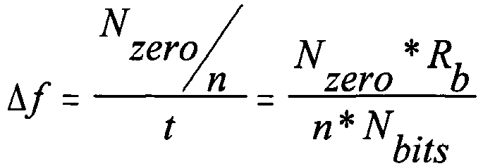
- wherein: Rb is the bit rate on a single QPSK component I' or Q' (the symbol rate);
- Nbits is the number of processed I' or Q' bits during the time period (number of processed symbols); and
- n is the number of zero-crossing transitions monitored by the detector 306 (for example, if only the a) crossing was monitored, then n=1).
- Again, this conversion comprises a multiplication by a constant.
- The logical expressions for detecting transitions and zero-crossings may be implemented by the counter-clockwise transition detector, the clockwise transition detector and the zero-crossing detector (of any embodiment shown herein) in any suitable technological manner (for example, in hardware, software, firmware, or the like, including combinations thereof). For example, the logic circuit implementations illustrated in
FIGURES 3A-3D and4A-4D (or equivalents, or simplifications, or combinations) may be utilized if appropriate for the detector application. Alternatively, the logical expressions may be coded in software running as an application, or implemented through the use of a digital signal processor or programmable array. Furthermore, it should be recognized, as discussed above, that the logical expressions for detecting transitions (event (1) AND event (2)) incorporate the logical expressions for zero-crossings (event (2)), and thus a separate physical implementation for zero-crossing detection is not required (this is graphically illustrated by the dotted line functionality within the clockwise and counter-clockwise transition detectors inFIGURES 6-8 ). - The detection of a corresponding pair of transitions (for example, first to second and second to first, as mentioned above) is sufficient to provide information for making a frequency offset magnitude and direction determination. By increasing the number of transition pairs detected, however, the accuracy of the magnitude determination improves. Thus, if a given implementation of the detector requires a high degree of accuracy in the measured magnitude of the determined frequency offset, the counter-clockwise transition detector and the clockwise transition detector should implement plural (up to the maximum of four if possible) pairs of transition detections.
- Reference is now made to
FIGURE 9 wherein there is shown a block diagram of UMTS-FDD cell searcher 500 implementing the frequency offset detector of the present invention. Thecell searcher 500 performs signal acquisition in three steps. In a first step (often referred to in the art as "step 1"), slot acquisition (or slot synchronization) 502 is performed. In thisstep 1 process, thecell searcher 500 synchronizes itself to the time slots of the received signal by detecting the beginnings of each slot through a correlation process where the received signal is correlated against a primary synchronization code. In the second step (often referred to in the art as "step 2"), frame acquisition (or frame synchronization) 504 is performed. In thisstep 2 process, thecell searcher 500 synchronizes itself to the frame alignment (where a frame comprises 15 consecutive slots) through a correlation process where the received signal at each slot location is correlated against a secondary synchronization code. This frame alignment process not only detects the beginning of the frame, but also detects which sequence of codes are present in the received signal (and thus identifies the scrambling code used by the base station). In the third step (often referred to in the art as "step 3"), base station identification (or scrambling code acquisition) 506 is performed. In thisstep 3 process, thecell searcher 500 identifies the unique code used by the base station to scramble its transmitted data. - The frequency offset detector (100, 200, 300 and 400) of the present invention is particularly useful in connection with the performance of the
step 3 process forbase station identification 506. Although any of the detectors shown inFIGURES 5-8 may be used in thecell searcher 500, as a practical matter thedetector 400 provides the best accuracy and would be preferred for a UMTS-FDD application. The I and Q (more specifically, the I' and Q') components of the primary common pilot channel (P-CPICH) are retrieved. Although the I and Q components have identical data contents (e.g., all ones), they are different because the scrambling code is complex in nature. So, the CPICH is actually the same as the scrambling code (during one frame). Although the I and Q components differ, they do not need to be retrieved separately, since this is the final step of the signal acquisition phase. Actually, the correct scrambling code is identified by correlating the complex input signal with the conjugate of one of the eight assumed scrambling codes (where this group of eight candidate codes for the actual scrambling code is an outcome of thestep 2 process in addition to the frame synchronization). Correlating the complex input signal with the conjugate of an assumed scrambling codes is performed as follows:
- wherein: I' is the "in-phase" signal vector I';
- Is is the real part of the assumed scrambling code;
- Q' is the "quadrature" signal vector;
- Qs is the imaginary part of the assumed scrambling code;
- E is the "energy" (i.e., the correlation result); and
- T refers to a transposition.
- In the presence of phase error (Φ), I' and Q' are:


- Thus:

references FIGURES 5-8 )) takes into account the phase components I'Is_true and Q'Qs_true, referred to herein as I' and Q', respectively, which already had to be computed for finding the correlation peak (value E). By estimating the number of "sector crossings" in I' and Q' (more precisely, I'Is and Q'Qs), the present invention computes the frequency offset (solid line) or information indicative of the frequency offset (dotted line). This information (sign and magnitude) can then be fed back 508 to the automaticfrequency control loop 510 of the receiver to improve its operation. - Although preferred embodiments of the method and apparatus of the present invention have been illustrated in the accompanying Drawings and described in the foregoing Detailed Description, it will be understood that the invention is not limited to the embodiments disclosed, but is capable of numerous rearrangements, modifications and substitutions without departing from the invention as set forth and defined by the following claims.
Claims (22)
- A frequency offset detector (100;200;300;400) for measuring the sign and magnitude of a frequency offset between a local oscillator frequency at a receiver and the frequency of a received complex signal, comprising:a first detector (102;202)adapted to detect at least one quadrant transition of the received complex signal in a counter-clockwise rotation direction;a first accumulator (108(1);208(1);408(1))adapted to accumulate a number of counter-clockwise quadrant transitions detected by the first detector during a time period;a second detector (104;204)adapted to detect at least one corresponding quadrant transition of the received complex signal in a clockwise rotation direction;a second accumulator (108(2);208(2);408(2))adapted to accumulate a number of clockwise quadrant transitions detected by the second detector during the same time period; characterized by comparing means (112,120;212,216;412,416) adapted to compare the accumulated counter-clockwise quadrant transitions with the clockwise quadrant transitions to obtain a difference value, a sign of that difference value being indicative of the frequency offset sign and a magnitude of that difference value being indicative of the frequency offset magnitude; andmeans (508,510) for adjusting operation of a receiver frequency control loop in accordance with the sign and magnitude.
- The detector as in claim 1 comprising a processing component (112) providing the comparing means and adapted to reset the first and second accumulators at the end of each time period.
- The detector as in claim 1 or 2 wherein the received complex signal is quantized by a single I bit and a single Q bit, and wherein the first and second detector operate to detect quadrant transitions by examining the single bits.
- A frequency offset detector as in claim 1, wherein the comparing means comprises a subtractor (116) adapted to subtract from the accumulated counter-clockwise quadrant transitions the clockwise quadrant transitions to obtain said difference value.
- A frequency offset detector as in claim 1 comprising:a third detector (206;306) operating to detect at least one zero-crossing on one component of the received complex signal;a third accumulator (208(3),408(3)) that accumulates a number of zero-crossings detected by the third detector during the same time period; anda comparator (216) that compares the difference value to a threshold, a magnitude of that difference value being indicative of the frequency offset magnitude if the threshold is not exceeded, and the accumulated zero-crossings being indicative of the frequency offset magnitude if the threshold is exceeded.
- The detector as in any preceding claim further including a processing component (212) adapted to calculate the frequency offset magnitude by dividing (222,322,422) the difference value by the time period.
- The detector as in claim 6 wherein the first and second detectors (102,202;104,204) each detect two or four corresponding quadrant transitions, and wherein the processing component calculates the frequency offset magnitude by dividing the difference value by two or four times the time period.
- The detector as in claims 5 and 6, wherein the processing component (212) calculates a value proportional to the frequency offset magnitude by dividing the accumulated zero-crossings by the time period.
- The detector as in claims 5 and 6, wherein the zero-crossing detector (206) detects two or four separate zero-crossings, and wherein the processing component calculates a value proportional to the frequency offset magnitude by dividing the accumulated zero-crossings by two or four times the time period.
- The detector as in claim 6 or any claim appended thereto wherein the processing component (212) is adapted to reset the first, second and third accumulators at the end of each time period.
- The detector as in claim 5 or any claim appended thereto wherein the received complex signal is quantized by a single I bit and a single Q bit, and wherein the first, second and third detectors each operate to make detections by examining the single bits.
- The detector as in claim 3 or any claim appended thereto or claim 11 wherein the quantized single I and Q bits are sign bits of the I and Q components of the received complex signal.
- The detector as in claim 5 or any claim dependent thereon, wherein the third detector (306) is adapted to detect zero-crossings in a non-redundant manner and/or in either direction of rotation.
- The detector as in claim 5 or any claim appended thereto wherein the third detector is incorporated within the first and second detectors.
- A method for measuring the sign and magnitude of a frequency offset between a local oscillator frequency at a receiver and the frequency of a received complex signal, comprising:detecting at least one quadrant transition of the received complex signal in a counter-clockwise rotation direction;accumulating a number of counter-clockwise quadrant transitions during a time period;detecting at least one corresponding quadrant transition of the received complex signal in a clockwise rotation direction;accumulating a number of clockwise quadrant transitions during the same time period; characterized by comparing the accumulated counter-clockwise quadrant transitions with the clockwise quadrant transitions to obtain a difference value;providing a sign of that difference value as being indicative of the frequency offset sign;providing a magnitude of that difference value being indicative of the frequency offset magnitude; andadjusting operation of a receiver frequency control loop in accordance with the sign and magnitude.
- The method as in claim 15 wherein the step of providing a magnitude comprises the step of calculating a value proportional to the frequency offset magnitude by dividing the difference value by the time period.
- The method as in claim 15, wherein the step of comparing comprises subtracting from the accumulated counter-clockwise quadrant transitions the clockwise quadrant transitions to obtain the difference value.
- A method as in claim 15 or 17 comprising:accumulating a number of zero-crossings during the same time period;comparing the difference value to a threshold;providing a magnitude of that difference value as being indicative of the frequency offset magnitude if the threshold is not exceeded; andproviding the accumulated zero-crossings being indicative of the frequency offset magnitude if the threshold is exceeded.
- The method as in any of claims 15 to 18 wherein the step of providing a magnitude comprises the step of calculating a value proportional to the frequency offset magnitude by dividing the difference value by the time period.
- The method as in any of claims 15 to 19 wherein the step of providing comprises the step of calculating a value proportional to the frequency offset magnitude by dividing the accumulated zero-crossings by the time period.
- The method as in any of claims 15 to 20 wherein the received complex signal is quantized by a single I bit and a single Q bit, and wherein the detecting steps detect quadrant transitions and/or zero-crossings by examining the single bits.
- The method as in claims 21 wherein the quantized single I and Q bits are sign bits of the I and Q components of the received complex signal.
Applications Claiming Priority (3)
| Application Number | Priority Date | Filing Date | Title |
|---|---|---|---|
| US10/154,233 US7075948B2 (en) | 2002-05-22 | 2002-05-22 | Frequency offset estimator |
| EP03253183A EP1389860A3 (en) | 2002-05-22 | 2003-05-21 | Frequency offset estimator |
| EP05076104A EP1566933B1 (en) | 2002-05-22 | 2003-05-21 | Cell search with frequency offset estimation |
Related Parent Applications (2)
| Application Number | Title | Priority Date | Filing Date |
|---|---|---|---|
| EP03253183A Division EP1389860A3 (en) | 2002-05-22 | 2003-05-21 | Frequency offset estimator |
| EP05076104A Division EP1566933B1 (en) | 2002-05-22 | 2003-05-21 | Cell search with frequency offset estimation |
Publications (2)
| Publication Number | Publication Date |
|---|---|
| EP1848169A1 EP1848169A1 (en) | 2007-10-24 |
| EP1848169B1 true EP1848169B1 (en) | 2018-01-24 |
Family
ID=29548828
Family Applications (3)
| Application Number | Title | Priority Date | Filing Date |
|---|---|---|---|
| EP07075540.0A Expired - Lifetime EP1848169B1 (en) | 2002-05-22 | 2003-05-21 | Frequency offset estimator |
| EP03253183A Withdrawn EP1389860A3 (en) | 2002-05-22 | 2003-05-21 | Frequency offset estimator |
| EP05076104A Expired - Lifetime EP1566933B1 (en) | 2002-05-22 | 2003-05-21 | Cell search with frequency offset estimation |
Family Applications After (2)
| Application Number | Title | Priority Date | Filing Date |
|---|---|---|---|
| EP03253183A Withdrawn EP1389860A3 (en) | 2002-05-22 | 2003-05-21 | Frequency offset estimator |
| EP05076104A Expired - Lifetime EP1566933B1 (en) | 2002-05-22 | 2003-05-21 | Cell search with frequency offset estimation |
Country Status (4)
| Country | Link |
|---|---|
| US (3) | US7075948B2 (en) |
| EP (3) | EP1848169B1 (en) |
| JP (1) | JP2004007692A (en) |
| DE (1) | DE60327460D1 (en) |
Families Citing this family (32)
| Publication number | Priority date | Publication date | Assignee | Title |
|---|---|---|---|---|
| AU2003225815A1 (en) * | 2002-03-19 | 2003-10-08 | Powerwave Technologies, Inc. | System and method for eliminating signal zero crossings in single and multiple channel communication systems |
| US7292624B2 (en) * | 2002-08-27 | 2007-11-06 | Itt Manufacturing, Inc. | Method and apparatus for robust acquisition of spread spectrum signals |
| WO2004034231A2 (en) * | 2002-10-11 | 2004-04-22 | Flint Hills Scientific, L.L.C. | Intrinsic timescale decomposition, filtering, and automated analysis of signals of arbitrary origin or timescale |
| NZ524369A (en) * | 2003-02-24 | 2005-05-27 | Tait Electronics Ltd | Improvements relating to frequency estimation |
| US7209716B2 (en) * | 2003-02-27 | 2007-04-24 | Ntt Docomo, Inc. | Radio communication system, radio station, and radio communication method |
| US7477713B2 (en) * | 2004-03-02 | 2009-01-13 | International Business Machines Corporation | method for providing automatic adaptation to frequency offsets in high speed serial links |
| US7349457B2 (en) * | 2004-03-29 | 2008-03-25 | Aeroflex Powel, Inc. | Broadband frequency agile signal characterization |
| US7756193B2 (en) * | 2006-09-21 | 2010-07-13 | Broadcom Corporation | Time divided pilot channel detection processing in WCDMA terminal having shared memory |
| US7720131B2 (en) | 2007-02-02 | 2010-05-18 | Pc-Tel, Inc. | Iterative pilot-aided frequency offset estimation and C/I measurement for TDMA signal with offset larger than nyquist frequency of the reference symbol rate |
| JP2010271091A (en) | 2009-05-20 | 2010-12-02 | Seiko Epson Corp | Frequency measuring device |
| JP5440999B2 (en) * | 2009-05-22 | 2014-03-12 | セイコーエプソン株式会社 | Frequency measuring device |
| JP5517033B2 (en) | 2009-05-22 | 2014-06-11 | セイコーエプソン株式会社 | Frequency measuring device |
| US8401123B2 (en) * | 2009-07-28 | 2013-03-19 | Broadcom Corporation | Method and system for increasing the accuracy of frequency offset estimation in multiple frequency hypothesis testing in an E-UTRA/LTE UE receiver |
| US8380151B2 (en) | 2009-12-18 | 2013-02-19 | Broadcom Corporation | Method and system for reducing the complexity of multi-frequency hypothesis testing using an iterative approach |
| US8462647B2 (en) * | 2009-07-28 | 2013-06-11 | Broadcom Corporation | Method and system for multiple frequency hypothesis testing with full synch acquisition in an E-UTRA/LTE UE receiver |
| US8369279B2 (en) | 2010-03-10 | 2013-02-05 | Broadcom Corporation | Method and system for iterative multiple frequency hypothesis testing with cell-ID detection in an E-UTRA/LTE UE receiver |
| JP5582447B2 (en) | 2009-08-27 | 2014-09-03 | セイコーエプソン株式会社 | Electric circuit, sensor system including the electric circuit, and sensor device including the electric circuit |
| JP5815918B2 (en) | 2009-10-06 | 2015-11-17 | セイコーエプソン株式会社 | Frequency measuring method, frequency measuring apparatus, and apparatus provided with frequency measuring apparatus |
| JP5876975B2 (en) | 2009-10-08 | 2016-03-02 | セイコーエプソン株式会社 | Frequency measuring device and method of generating shift frequency division signal in frequency measuring device |
| US8917704B2 (en) | 2009-12-18 | 2014-12-23 | Broadcom Corporation | Method and system for automatically rescaling an accumulation buffer in synchronization systems |
| US8897656B2 (en) * | 2010-07-08 | 2014-11-25 | Em Photonics, Inc. | Synchronizing phases of multiple opitcal channels |
| JP5883558B2 (en) | 2010-08-31 | 2016-03-15 | セイコーエプソン株式会社 | Frequency measuring device and electronic device |
| US8477885B2 (en) | 2011-01-21 | 2013-07-02 | Northrop Grumman Systems Corporation | Recursive frequency estimation |
| ES2402632B1 (en) | 2011-02-08 | 2014-05-14 | Tyco Electronics Raychem Bvba | RELEASE TONGUE FOR AN ELECTRICAL CONNECTOR AND ELECTRICAL CONNECTOR THAT INCLUDES SUCH RELEASE TONGUE |
| ES2395358B1 (en) | 2011-02-08 | 2014-04-25 | Tyco Electronics Corporation | SINGLE ACTION CONNECTOR |
| CN103257407B (en) | 2012-02-20 | 2015-11-25 | 泰科电子(上海)有限公司 | Connector and connector assembly |
| US9152929B2 (en) | 2013-01-23 | 2015-10-06 | Splunk Inc. | Real time display of statistics and values for selected regular expressions |
| ES2879918T3 (en) | 2014-01-13 | 2021-11-23 | Commscope Telecommunications Shanghai Co Ltd | Fiber optic connector |
| CN106941468B (en) * | 2016-01-05 | 2019-11-12 | 中国移动通信集团公司 | The frequency deviation estimating method and device of long evolving system |
| MX2019006853A (en) * | 2016-12-19 | 2019-08-22 | Ericsson Telefon Ab L M | Systems and methods for switching reference crystal oscillators for a transceiver of a wireless device. |
| WO2018226959A1 (en) | 2017-06-07 | 2018-12-13 | Commscope Technologies Llc | Fiber optic adapter and cassette |
| CN110068842B (en) * | 2019-05-06 | 2021-01-29 | 西安开阳微电子有限公司 | High-precision satellite signal capturing method |
Family Cites Families (33)
| Publication number | Priority date | Publication date | Assignee | Title |
|---|---|---|---|---|
| JPH0654509B2 (en) * | 1988-08-11 | 1994-07-20 | 株式会社日本コンラックス | Coin sorting accuracy setting device |
| GB2232852B (en) * | 1989-05-31 | 1993-10-27 | Technophone Ltd | Offset correction |
| US5376894A (en) * | 1992-12-31 | 1994-12-27 | Pacific Communication Sciences, Inc. | Phase estimation and synchronization using a PSK demodulator |
| US5590158A (en) * | 1993-01-28 | 1996-12-31 | Advantest Corporation | Method and apparatus for estimating PSK modulated signals |
| FR2726141B1 (en) * | 1994-10-25 | 1997-01-03 | Alcatel Mobile Comm France | CORRECTION OF A FREQUENCY OFFSET |
| JP3390272B2 (en) * | 1994-11-10 | 2003-03-24 | 沖電気工業株式会社 | Synchronous detection circuit |
| US5748682A (en) * | 1994-12-16 | 1998-05-05 | Lucent Technologies Inc. | Oscillator frequency offset error estimator for communications systems |
| US5640431A (en) * | 1995-03-10 | 1997-06-17 | Motorola, Inc. | Method and apparatus for offset frequency estimation for a coherent receiver |
| JP3200547B2 (en) * | 1995-09-11 | 2001-08-20 | 株式会社日立製作所 | CDMA mobile communication system |
| US5732111A (en) * | 1995-12-06 | 1998-03-24 | Rockwell International Corporation | Frequency error compensation for direct sequence spread spectrum systems |
| US6160841A (en) * | 1996-05-24 | 2000-12-12 | Leica Geosystems Inc. | Mitigation of multipath effects in global positioning system receivers |
| US5946360A (en) * | 1997-03-27 | 1999-08-31 | Lucent Technologies Inc. | Frequency offset compensation using dotting sequences |
| US5799043A (en) * | 1997-06-02 | 1998-08-25 | Motorola, Inc. | Method and apparatus for decoding a two-level radio signal |
| JP3316744B2 (en) * | 1997-10-30 | 2002-08-19 | 三菱電機株式会社 | AFC circuit, receiver having the same, and automatic frequency control communication system |
| US6134260A (en) * | 1997-12-16 | 2000-10-17 | Ericsson Inc. | Method and apparatus for frequency acquisition and tracking for DS-SS CDMA receivers |
| US6266361B1 (en) * | 1998-07-21 | 2001-07-24 | Chung-Shan Institute Of Science And Technology | Method and architecture for correcting carrier frequency offset and spreading code timing offset in a direct sequence spread spectrum communication system |
| US6324227B1 (en) * | 1998-09-09 | 2001-11-27 | Qualcomm Incorporated | Receiver for performing position location with efficient rotator |
| EP1035665A1 (en) * | 1999-03-10 | 2000-09-13 | Robert Bosch Gmbh | Method for the initial synchronization of a digital mobile radio system |
| US6560298B1 (en) * | 1999-05-25 | 2003-05-06 | Motorola, Inc. | Method and apparatus for concurrent synchronization and improved automatic frequency control in a communication device |
| JP2001016135A (en) * | 1999-06-29 | 2001-01-19 | Nec Corp | Method and system for automatically controlling frequency and cdma receiver |
| US6463266B1 (en) * | 1999-08-10 | 2002-10-08 | Broadcom Corporation | Radio frequency control for communications systems |
| GB2359456B (en) * | 2000-02-19 | 2003-09-17 | Nec Technologies | Method for frequency offset estimation in a direct sequence spread spectrum communications receiver |
| US6466958B1 (en) * | 2000-09-12 | 2002-10-15 | Interstate Electronics Corporation, A Division Of L3 Communications Corporation | Parallel frequency searching in an acquisition correlator |
| US6628926B1 (en) * | 2000-10-11 | 2003-09-30 | Nokia Networks Oy | Method for automatic frequency control |
| US6661851B1 (en) * | 2000-10-20 | 2003-12-09 | Qualcomm Incorporated | Bi-directional vector rotator |
| JP2002141962A (en) * | 2000-11-01 | 2002-05-17 | Mitsubishi Electric Corp | Carrier recovery circuit and lock detection circuit |
| US6704555B2 (en) * | 2001-01-09 | 2004-03-09 | Qualcomm, Incorporated | Apparatus and method for calibrating local oscillation frequency in wireless communications |
| US6891880B2 (en) * | 2001-05-18 | 2005-05-10 | Global Locate, Inc. | Method and apparatus for performing signal correlation |
| US6744747B2 (en) * | 2001-08-22 | 2004-06-01 | Qualcomm, Incorporated | Method & apparatus for W-CDMA handoff searching |
| US7200162B2 (en) * | 2001-08-31 | 2007-04-03 | Qualcomm, Incorporated | Interpolation of channel search results |
| US7206298B2 (en) * | 2001-09-06 | 2007-04-17 | Qualcomm, Incorporated | Conducting searches amidst asynchronous cells of a communication system |
| US20030128777A1 (en) * | 2001-12-04 | 2003-07-10 | Linsky Stuart T. | Decision directed phase locked loops (DD-PLL) with multiple initial phase and/or frequency estimates in digital communication systems |
| US7369577B2 (en) * | 2002-05-16 | 2008-05-06 | Stmicroelectronics, Inc. | Code group acquisition procedure for a UMTS-FDD receiver |
-
2002
- 2002-05-22 US US10/154,233 patent/US7075948B2/en not_active Expired - Lifetime
-
2003
- 2003-05-21 EP EP07075540.0A patent/EP1848169B1/en not_active Expired - Lifetime
- 2003-05-21 EP EP03253183A patent/EP1389860A3/en not_active Withdrawn
- 2003-05-21 DE DE60327460T patent/DE60327460D1/en not_active Expired - Fee Related
- 2003-05-21 EP EP05076104A patent/EP1566933B1/en not_active Expired - Lifetime
- 2003-05-22 JP JP2003145156A patent/JP2004007692A/en active Pending
-
2006
- 2006-06-29 US US11/480,205 patent/US7430402B2/en not_active Expired - Lifetime
-
2008
- 2008-09-23 US US12/235,757 patent/US7764937B2/en not_active Expired - Lifetime
Non-Patent Citations (1)
| Title |
|---|
| None * |
Also Published As
| Publication number | Publication date |
|---|---|
| US20060246865A1 (en) | 2006-11-02 |
| EP1566933A2 (en) | 2005-08-24 |
| US7764937B2 (en) | 2010-07-27 |
| JP2004007692A (en) | 2004-01-08 |
| EP1566933B1 (en) | 2009-04-29 |
| DE60327460D1 (en) | 2009-06-10 |
| EP1389860A2 (en) | 2004-02-18 |
| US20090017768A1 (en) | 2009-01-15 |
| US7075948B2 (en) | 2006-07-11 |
| US20030220084A1 (en) | 2003-11-27 |
| US7430402B2 (en) | 2008-09-30 |
| EP1566933A3 (en) | 2005-08-31 |
| EP1389860A3 (en) | 2004-04-07 |
| EP1848169A1 (en) | 2007-10-24 |
Similar Documents
| Publication | Publication Date | Title |
|---|---|---|
| EP1848169B1 (en) | Frequency offset estimator | |
| US7203254B2 (en) | Method and system for synchronizing in a frequency shift keying receiver | |
| US7239675B2 (en) | GFSK receiver | |
| US7426234B2 (en) | Synchronization signal detector and method | |
| CA2103299C (en) | Frequency offset estimation using the phase rotation of channel estimates | |
| US6266361B1 (en) | Method and architecture for correcting carrier frequency offset and spreading code timing offset in a direct sequence spread spectrum communication system | |
| JPH0821961B2 (en) | Digital demodulator, differential phase shift keying demodulator, and low signal-to-noise ratio input signal demodulation method | |
| US6693882B1 (en) | Frequency correction burst detection | |
| US10855494B2 (en) | Transmitter and receiver and corresponding methods | |
| EP1191704A2 (en) | Method and apparatus for acquiring slot timing and frequency offset correction | |
| CN113726347B (en) | Transmitter, receiver and method for chirp modulated radio signals | |
| US6603821B1 (en) | Wireless communication terminal capable of correctly specifying position of burst and having small frequency error of recovered carrier | |
| US5732105A (en) | Method of estimating signal quality in a DPSK demodulator | |
| CN108347396B (en) | System and method for tracking and compensating timing offset and frequency offset of modulated signal | |
| EP4087176A2 (en) | Radio receiver synchronization | |
| EP0783206A2 (en) | Data synchronizer lock detector and method of operation thereof | |
| US7315588B2 (en) | System and method for enhanced acquisition for large frequency offsets and poor signal to noise ratio | |
| EP1112634A1 (en) | Carrier frequency estimator for a signal receiver | |
| JP3789157B2 (en) | Frequency error estimation device | |
| US7239658B1 (en) | Coherent demodulation of hopped MSK waveforms system and method | |
| US10530905B1 (en) | Frame delimiter detection | |
| JP3877607B2 (en) | Offset frequency detection method and synchronization deviation amount detection method | |
| JPH0446428A (en) | Demodulator for spread spectrum communication |
Legal Events
| Date | Code | Title | Description |
|---|---|---|---|
| PUAI | Public reference made under article 153(3) epc to a published international application that has entered the european phase |
Free format text: ORIGINAL CODE: 0009012 |
|
| AC | Divisional application: reference to earlier application |
Ref document number: 1566933 Country of ref document: EP Kind code of ref document: P Ref document number: 1389860 Country of ref document: EP Kind code of ref document: P |
|
| AK | Designated contracting states |
Kind code of ref document: A1 Designated state(s): AT BE BG CH CY CZ DE DK EE ES FI FR GB GR HU IE IT LI LU MC NL PT RO SE SI SK TR |
|
| AX | Request for extension of the european patent |
Extension state: AL LT LV MK |
|
| 17P | Request for examination filed |
Effective date: 20080314 |
|
| 17Q | First examination report despatched |
Effective date: 20080409 |
|
| AKX | Designation fees paid |
Designated state(s): DE FR GB IT |
|
| RAP1 | Party data changed (applicant data changed or rights of an application transferred) |
Owner name: STMICROELECTRONICS, INC. |
|
| RAP1 | Party data changed (applicant data changed or rights of an application transferred) |
Owner name: STMICROELECTRONICS INTERNATIONAL N.V. |
|
| RAP1 | Party data changed (applicant data changed or rights of an application transferred) |
Owner name: FRANCE BREVETS |
|
| REG | Reference to a national code |
Ref country code: DE Ref legal event code: R079 Ref document number: 60350946 Country of ref document: DE Free format text: PREVIOUS MAIN CLASS: H04L0027233000 Ipc: H04L0027000000 |
|
| GRAP | Despatch of communication of intention to grant a patent |
Free format text: ORIGINAL CODE: EPIDOSNIGR1 |
|
| STAA | Information on the status of an ep patent application or granted ep patent |
Free format text: STATUS: GRANT OF PATENT IS INTENDED |
|
| RIC1 | Information provided on ipc code assigned before grant |
Ipc: H04L 27/00 20060101AFI20170721BHEP Ipc: H04B 7/26 20060101ALI20170721BHEP Ipc: H04L 27/227 20060101ALI20170721BHEP Ipc: H04L 27/233 20060101ALI20170721BHEP |
|
| INTG | Intention to grant announced |
Effective date: 20170816 |
|
| GRAS | Grant fee paid |
Free format text: ORIGINAL CODE: EPIDOSNIGR3 |
|
| GRAA | (expected) grant |
Free format text: ORIGINAL CODE: 0009210 |
|
| STAA | Information on the status of an ep patent application or granted ep patent |
Free format text: STATUS: THE PATENT HAS BEEN GRANTED |
|
| AC | Divisional application: reference to earlier application |
Ref document number: 1389860 Country of ref document: EP Kind code of ref document: P Ref document number: 1566933 Country of ref document: EP Kind code of ref document: P |
|
| AK | Designated contracting states |
Kind code of ref document: B1 Designated state(s): DE FR GB IT |
|
| REG | Reference to a national code |
Ref country code: GB Ref legal event code: FG4D |
|
| REG | Reference to a national code |
Ref country code: DE Ref legal event code: R096 Ref document number: 60350946 Country of ref document: DE |
|
| REG | Reference to a national code |
Ref country code: FR Ref legal event code: PLFP Year of fee payment: 16 |
|
| REG | Reference to a national code |
Ref country code: DE Ref legal event code: R097 Ref document number: 60350946 Country of ref document: DE |
|
| PG25 | Lapsed in a contracting state [announced via postgrant information from national office to epo] |
Ref country code: IT Free format text: LAPSE BECAUSE OF FAILURE TO SUBMIT A TRANSLATION OF THE DESCRIPTION OR TO PAY THE FEE WITHIN THE PRESCRIBED TIME-LIMIT Effective date: 20180124 |
|
| PLBE | No opposition filed within time limit |
Free format text: ORIGINAL CODE: 0009261 |
|
| STAA | Information on the status of an ep patent application or granted ep patent |
Free format text: STATUS: NO OPPOSITION FILED WITHIN TIME LIMIT |
|
| 26N | No opposition filed |
Effective date: 20181025 |
|
| PGFP | Annual fee paid to national office [announced via postgrant information from national office to epo] |
Ref country code: GB Payment date: 20220414 Year of fee payment: 20 Ref country code: FR Payment date: 20220422 Year of fee payment: 20 Ref country code: DE Payment date: 20220420 Year of fee payment: 20 |
|
| REG | Reference to a national code |
Ref country code: DE Ref legal event code: R071 Ref document number: 60350946 Country of ref document: DE |
|
| REG | Reference to a national code |
Ref country code: GB Ref legal event code: PE20 Expiry date: 20230520 |
|
| PG25 | Lapsed in a contracting state [announced via postgrant information from national office to epo] |
Ref country code: GB Free format text: LAPSE BECAUSE OF EXPIRATION OF PROTECTION Effective date: 20230520 |