EP1848033A2 - Semiconductor Device and Fabrication Method Therefor - Google Patents
Semiconductor Device and Fabrication Method Therefor Download PDFInfo
- Publication number
- EP1848033A2 EP1848033A2 EP07105228A EP07105228A EP1848033A2 EP 1848033 A2 EP1848033 A2 EP 1848033A2 EP 07105228 A EP07105228 A EP 07105228A EP 07105228 A EP07105228 A EP 07105228A EP 1848033 A2 EP1848033 A2 EP 1848033A2
- Authority
- EP
- European Patent Office
- Prior art keywords
- gate electrode
- film
- insulating film
- metal
- semiconductor device
- Prior art date
- Legal status (The legal status is an assumption and is not a legal conclusion. Google has not performed a legal analysis and makes no representation as to the accuracy of the status listed.)
- Withdrawn
Links
Images



Classifications
-
- H—ELECTRICITY
- H10—SEMICONDUCTOR DEVICES; ELECTRIC SOLID-STATE DEVICES NOT OTHERWISE PROVIDED FOR
- H10D—INORGANIC ELECTRIC SEMICONDUCTOR DEVICES
- H10D84/00—Integrated devices formed in or on semiconductor substrates that comprise only semiconducting layers, e.g. on Si wafers or on GaAs-on-Si wafers
- H10D84/01—Manufacture or treatment
- H10D84/0123—Integrating together multiple components covered by H10D12/00 or H10D30/00, e.g. integrating multiple IGBTs
- H10D84/0126—Integrating together multiple components covered by H10D12/00 or H10D30/00, e.g. integrating multiple IGBTs the components including insulated gates, e.g. IGFETs
- H10D84/0135—Manufacturing their gate conductors
- H10D84/0137—Manufacturing their gate conductors the gate conductors being silicided
-
- H—ELECTRICITY
- H10—SEMICONDUCTOR DEVICES; ELECTRIC SOLID-STATE DEVICES NOT OTHERWISE PROVIDED FOR
- H10D—INORGANIC ELECTRIC SEMICONDUCTOR DEVICES
- H10D84/00—Integrated devices formed in or on semiconductor substrates that comprise only semiconducting layers, e.g. on Si wafers or on GaAs-on-Si wafers
- H10D84/01—Manufacture or treatment
- H10D84/0123—Integrating together multiple components covered by H10D12/00 or H10D30/00, e.g. integrating multiple IGBTs
- H10D84/0126—Integrating together multiple components covered by H10D12/00 or H10D30/00, e.g. integrating multiple IGBTs the components including insulated gates, e.g. IGFETs
- H10D84/0135—Manufacturing their gate conductors
- H10D84/014—Manufacturing their gate conductors the gate conductors having different materials or different implants
-
- H—ELECTRICITY
- H10—SEMICONDUCTOR DEVICES; ELECTRIC SOLID-STATE DEVICES NOT OTHERWISE PROVIDED FOR
- H10D—INORGANIC ELECTRIC SEMICONDUCTOR DEVICES
- H10D84/00—Integrated devices formed in or on semiconductor substrates that comprise only semiconducting layers, e.g. on Si wafers or on GaAs-on-Si wafers
- H10D84/01—Manufacture or treatment
- H10D84/0123—Integrating together multiple components covered by H10D12/00 or H10D30/00, e.g. integrating multiple IGBTs
- H10D84/0126—Integrating together multiple components covered by H10D12/00 or H10D30/00, e.g. integrating multiple IGBTs the components including insulated gates, e.g. IGFETs
- H10D84/0165—Integrating together multiple components covered by H10D12/00 or H10D30/00, e.g. integrating multiple IGBTs the components including insulated gates, e.g. IGFETs the components including complementary IGFETs, e.g. CMOS devices
- H10D84/0172—Manufacturing their gate conductors
- H10D84/0174—Manufacturing their gate conductors the gate conductors being silicided
-
- H—ELECTRICITY
- H10—SEMICONDUCTOR DEVICES; ELECTRIC SOLID-STATE DEVICES NOT OTHERWISE PROVIDED FOR
- H10D—INORGANIC ELECTRIC SEMICONDUCTOR DEVICES
- H10D84/00—Integrated devices formed in or on semiconductor substrates that comprise only semiconducting layers, e.g. on Si wafers or on GaAs-on-Si wafers
- H10D84/01—Manufacture or treatment
- H10D84/0123—Integrating together multiple components covered by H10D12/00 or H10D30/00, e.g. integrating multiple IGBTs
- H10D84/0126—Integrating together multiple components covered by H10D12/00 or H10D30/00, e.g. integrating multiple IGBTs the components including insulated gates, e.g. IGFETs
- H10D84/0165—Integrating together multiple components covered by H10D12/00 or H10D30/00, e.g. integrating multiple IGBTs the components including insulated gates, e.g. IGFETs the components including complementary IGFETs, e.g. CMOS devices
- H10D84/0172—Manufacturing their gate conductors
- H10D84/0177—Manufacturing their gate conductors the gate conductors having different materials or different implants
-
- H—ELECTRICITY
- H10—SEMICONDUCTOR DEVICES; ELECTRIC SOLID-STATE DEVICES NOT OTHERWISE PROVIDED FOR
- H10D—INORGANIC ELECTRIC SEMICONDUCTOR DEVICES
- H10D84/00—Integrated devices formed in or on semiconductor substrates that comprise only semiconducting layers, e.g. on Si wafers or on GaAs-on-Si wafers
- H10D84/01—Manufacture or treatment
- H10D84/02—Manufacture or treatment characterised by using material-based technologies
- H10D84/03—Manufacture or treatment characterised by using material-based technologies using Group IV technology, e.g. silicon technology or silicon-carbide [SiC] technology
- H10D84/038—Manufacture or treatment characterised by using material-based technologies using Group IV technology, e.g. silicon technology or silicon-carbide [SiC] technology using silicon technology, e.g. SiGe
Definitions
- the present invention relates to a semiconductor device and a fabrication method therefor and, more particularly, to a semiconductor device comprising an n-channel MOS transistor and a p-channel MOS transistor and a fabrication method therefor.
- MOSFETs metal-oxide-film semiconductor field-effect transistors
- HfO 2 hafnium dioxide
- ZrO 2 zirconium dioxide
- the use of the high dielectric constant material for the gate insulating film allows a reduction in leakage current even when the electrically effective thickness of the gate insulating film is reduced to a value lower than that of a gate insulating film made of silicon dioxide (SiO 2 ).
- a metal gate electrode using a film made of a metal or a compound having a metallic conductivity and a fully-silicided gate electrode using a polysilicon film that has been fully silicided to the interface with a gate insulating film have been proposed (see, e.g., Japanese Laid-Open Patent Publication No. 2005-243678 ).
- the metal gate electrode or the fully-silicided gate electrode is used when the gate insulating film is made of a high dielectric constant material.
- a metal gate electrode or a fully-silicided gate electrode the merit of allowing the suppression of the depletion of a gate electrode is offered by using a metal gate electrode or a fully-silicided gate electrode. That is, in the operation of a transistor, the depletion of a polysilicon gate electrode which occurs when the channel polarity is inverted reduces the effective gate capacitance thereof. Therefore, by using the metal gate electrode or the fully-silicided gate electrode, it becomes possible to suppress the reduction in gate capacitance and obtain a larger current driving force.
- the metal gate electrode formed by depositing the metal film or the compound film having a metallic conductivity has the problem that electrode formation in a p-channel MOS transistor is difficult.
- the metal gate electrode can be formed by depositing a film made of titanium nitride (TaN), tantalum silicon nitride (TaSiN), or the like in terms of work function values.
- TaN titanium nitride
- TaSiN tantalum silicon nitride
- the merits of allowing a change in the intrinsic work function of TaN through a change in the amount of nitrogen and allowing the adjustment of the threshold voltage are also offered.
- the selection of a material for the metal gate electrode is relatively easy when the metal gate electrode is formed in the n-channel MOS transistor.
- the p-channel MOS transistor needs a large function, unlike the n-channel MOS transistor. Accordingly, for the p-channel MOS transistor, it is necessary to form the metal gate electrode by using a film made of a material containing a precious metal group including platinum (Pt), ruthenium (Ru), iridium (Ir), or the like. Because the film made of such a material containing a precious metal group has a large stress between itself and a gate insulating film, it has the problem that the formed electrode is likely to peel off. In addition, the film made of a material containing a precious metal group also has a problem associated with microfabrication because it is made of a material difficult to etch and the patterning thereof into the configuration of the gate electrode after film deposition is also difficult.
- a material containing a precious metal group including platinum (Pt), ruthenium (Ru), iridium (Ir), or the like. Because the film made of such a material containing a precious metal group has a large stress between itself
- CMOS complementary metal oxide film semiconductor
- the fully-silicided gate electrode formed by successively depositing the polysilicon film and a meal film made of nickel (Ni) or the like and then performing a thermal process to completely silicide a polysilicon electrode can be more easily formed than the metal gate electrode formed by directly depositing the metal film.
- the n-channel MOS transistor and the p-channel MOS transistor have different work functions that are optimal for gate electrodes.
- the work function of a fully-silicided gate electrode is determined by a composition ratio between Ni and Si.
- the composition ratio between Ni and Si after silicidation is determined by conditions for the thermal process during silicidation. As a result, a problem is encountered that it is extremely difficult to form the fully-silicided gate electrodes having different work functions in a single substrate.
- the present invention constructs a semiconductor device comprising a metal gate electrode and a fully-silicided gate electrode.
- a semiconductor device comprises: a transistor of a first conductivity formed on a semiconductor substrate and having a first gate insulating film and a first gate electrode; and a transistor of a second conductivity type formed on a different region of the semiconductor substrate from a region thereof on which the transistor of the first conductivity is formed and having a second gate insulating film and a second gate electrode, wherein the first gate electrode is a metal gate electrode having a metal film and the second gate electrode is a fully-silicided gate electrode.
- the semiconductor device according to the present invention allows easy individual formation of the first and second gate electrodes having different work functions. Therefore, it is possible to easily form a gate electrode having the work function optimal for an n-channel MOS transistor as the first gate electrode and form a gate electrode having the work function optimal for a p-channel MOS transistor as the second gate electrode. As a result, a semiconductor device in which each of the n-channel MOS transistor and the p-channel MOS transistor has a reduced leakage current and a low threshold voltage can be implemented.
- At least one of the first gate insulating film and the second gate insulating film is preferably made of a high dielectric constant material.
- the high dielectric constant material preferably contains at least one of silicon, hafnium, zirconium, titanium, tantalum, aluminum, and a rare earth metal.
- the transistor of the first conductivity type is preferably an n-channel MOS transistor and the transistor of the second conductivity type is preferably a p-channel MOS transistor.
- the arrangement allows the formation of gate electrodes which are individually optimal for the n-channel MOS transistor and the p-channel MOS transistor without using a material containing a precious metal group which is likely to cause the peeling off of the gate electrode from the gate insulating film and difficult to process.
- the metal film is preferably a single-layer film made of a material selected from the group consisting of Ta, TaN, TaSi, TaSiN, TaAl, TaAlN, TaAlSi, TaAlSiN, TaC, and TaCN or a multilayer film made of at least two materials selected from the group consisting of Ta, TaN, TaSi, TaSiN, TaAl, TaAlN, TaAlSi, TaAlSiN, TaC, and TaCN.
- the arrangement allows reliable reductions in the leakage current and threshold voltage of the n-channel MOS transistor.
- the arrangement also allows easy formation of the first gate electrode.
- the metal gate electrode preferably has a silicide film formed on the metal film.
- the arrangement provides easy connection between the gate electrode and a contact plug and also allows a reduction in the resistance value of the gate electrode.
- the first gate insulating film preferably has a thickness larger than a thickness of the second gate insulating film.
- the arrangement allows compensation for an increase in the gate leakage current of the n-channel MOS transistor due to a silicon dioxide film generated at the interface between the substrate made of silicon and the high dielectric constant film and allows the respective gate leakage currents of the n-channel MOS transistor and the p-channel MOS transistor to have equal characteristics.
- the fully-silicided gate electrode is preferably made of a silicide containing any one of Ni, Pt, and Co.
- a method for fabricating a semiconductor device comprises the steps of: (a) forming a first insulating film on a semiconductor substrate and then forming a metal film on the formed first insulating film; (b) removing respective portions of the first insulating film and the metal film which are located in a region of the semiconductor substrate to expose an upper surface of the semiconductor substrate; (c) forming a second insulating film on the exposed portion of the semiconductor substrate; (d) forming a polysilicon film over the metal film and the second insulating film; (e) patterning the polysilicon film formed on the metal film and the metal film to form a first gate electrode which is a metal gate electrode and patterning the polysilicon film formed on the second insulating film to form a second gate electrode; and (f) siliciding the patterned polysilicon film to change the second gate electrode into a fully-silicided gate electrode.
- the method for fabricating a semiconductor device according to the present invention allows easy individual formation of the metal gate electrode and the fully-silicided gate electrode without complicating the process steps. Because the first and second insulating films are formed individually, the respective gate insulating films of the n-channel MOS transistor and the p-channel MOS transistor can be easily formed to have different thicknesses.
- the step (c) preferably includes the sub-steps of: forming the second insulating film over the exposed portion of the semiconductor substrate and the metal film; and removing the portion of the second insulating film which is formed on the metal film.
- the method for fabricating a semiconductor device according to the present invention further comprises the step of: (g) after the step (e) and before the step (f), forming sidewalls on respective side surfaces of the first gate electrode and the second gate electrode.
- the method for fabricating a semiconductor device further comprises the step of: (h) after the step (g) and before the step (f), forming source/drain regions of a first conductivity type in respective portions of the semiconductor substrate which are located on both sides of the first gate electrode and forming source/drain regions of a second conductivity type in respective portions of the semiconductor substrate which are located on both sides of the second gate electrode; (i) after the step (h) and before the step (f), siliciding the source/drain regions of the first conductivity type and the source/drain regions of the second conductivity type; (j) after the step (d) and before the step (i), forming a third insulating film on the polysilicon film; and (k) after the step (j) and before the step (f), removing the third insulating film.
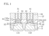
- FIG. 1 shows a cross-sectional structure of a semiconductor device according to the embodiment of the present invention.
- the semiconductor device according to the present embodiment comprises a p-channel MOS transistor and an n-channel MOS transistor which are formed on a substrate.
- a first region 11A and a second region 11B which are isolated from each other by an isolation region 12 are formed in a substrate 11 made of silicon.
- An n-channel MOS transistor 31 is formed in the first region 11A.
- the n-channel MOS transistor 31 has a first gate insulating film 32 made of hafnium dioxide (HfO 2 ) formed on the substrate 11 and a first gate electrode 33 comprising sidewalls 34. In the portions of the first region 11A which are located on both sides of the first gate electrode 33, n-type source/drain regions 35 are formed individually.
- the first gate electrode 33 in the semiconductor device according to the present embodiment is a metal gate electrode comprised of a metal film 14a made of TaN and a silicide film 26a made of platinum silicide which are successively stacked in layers in an ascending order, in which the metal film 14a is formed in contact with the first gate insulating film 32.
- the metal gate electrode is defined as a gate electrode formed such that a film made of a metal or a metal compound having a metallic conductivity is deposited in contact with a gate insulating film. It is assumed that the metal film in the metal gate electrode includes not only a film made of a metal but also a film made of a metal compound having a metallic conductivity.
- a p-channel MOS transistor 41 has a second gate insulating film 42 made of HfO 2 formed on the substrate 11 and a second gate electrode 43 comprising sidewalls 44. In the portions of the second region 11B which are located on both sides of the second gate electrode 43, p-type source/drain regions 45 are formed individually.
- the second gate electrode 43 is a fully-silicided gate electrode in which a silicide film 26b is formed on the second gate insulating film 42.
- the fully-silicided gate is a gate electrode formed by depositing a polysilicon film on a gate insulating film and then completely siliciding the deposited polysilicon film to the interface with the gate insulating film.
- the n-channel MOS transistor 31 and the p-channel MOS transistor 41 are covered with interlayer insulating films 24 and 27 formed in succession.
- interlayer insulating films 24 and 27 contact plugs 28 electrically connected individually to the first gate electrode 33, the n-type source/drain regions 35, the second gate electrode 43, and the p-type source/drain regions 45 are formed.
- the n-channel MOS transistor 31 has the first gate electrode 33 which is the metal gate electrode made of TaN and the p-channel MOS transistor 41 has the second gate electrode 43 which is the fully-silicided gate electrode.
- the gate electrodes having different work functions are formed individually in the n-channel MOS transistor 31 and the p-channel MOS transistor 41.
- a leakage current and a threshold voltage can be reduced.
- the fully-silicided gate electrode is formed in the p-channel MOS transistor 41.
- the peeling off of the gate electrode from the gate insulating film can be suppressed more reliably than in the case where a metal gate electrode using platinum (Pt) or the like is formed.
- the gate electrode can be formed more easily than in the case where the metal gate electrode is formed by etching Pt or the like.
- full silicidation can be performed under conditions which are optimal for the p-channel MOS transistor 41.
- a high dielectric constant film such as a hafnium silicate (HfSiO) film or a hafnium silicon oxynitride (HfSiON) film can be used as each of the first and second gate insulating films 32 and 42.
- a high dielectric constant film made of a material containing at least one of silicon (Si), hafnium (Hf), zirconium (Zr), titanium (Ti), tantalum (Ta), aluminum (Al), and rare earth metals such as scandium (Sc), yttrium (Y), lantern (La), and other lanthanoids may also be used.
- the first and second gate insulating films 32 and 43 may also be formed of different materials.
- a SiO 2 film may also be used.
- the merit of allowing the prevention of the depletion of the first gate electrode 33 and allowing the obtention of a transistor with a large driving current is offered.
- the metal film 14a of the first gate electrode 33 may also be made of, instead of TaN, a material selected from the group consisting of tantalum (Ta), tantalum silicon (TaSi), tantalum silicon nitride (TaSiN), tantalum aluminum (TaAl), tantalum aluminum nitride (TaAIN), tantalum aluminum silicon (TaAlSi), tantalum aluminum silicon nitride (TaAlSiN), tantalum carbide (TaC), tantalum carbide nitride (TaCN), and the like.
- the metal film 14a may also be a multilayer film made of at least two materials selected from the group listed above. In this case, the work function is preferably adjusted to be not less than 4.2 eV and not more than 4.5 eV. In the case where the metal film 14a is made of a nitride, the composition of nitrogen is preferably not more than 50%.
- the second gate electrode 43 may be made of, instead of platinum silicide, any of nickel silicide, cobalt silicide, and the like.
- the semiconductor device according to the present embodiment has formed the first gate electrode 33 by using a multilayer film of the metal film 14a and the silicide film 26a to provide easy connection between the contact plug 28 and the first gate electrode 33 and reduce the resistance value of the first gate electrode 33, it is also possible to form the first gate electrode 33 by using only the metal film 14a without providing the silicide film 26a.
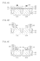
- FIGS. 2A to 6C illustrate the fabrication method for the semiconductor device according to the present embodiment in the order in which the process steps thereof are performed.
- the trench isolation region 12 is formed in the substrate 11 made of silicon so that the first region 11A in which the n-channel MOS transistor 31 is formed and the second region 11B in which the p-channel MOS transistor 41 is formed are formed.
- the isolation region may also be formed by using a localoxidation of silicon (LOCOS) technology.
- LOC localoxidation of silicon
- a native oxide film formed on the upper surface of the substrate 11 is removed by using a diluted aqueous fluoric acid solution. Then, a first insulating film 13 made of HfO 2 or the like and serving as the first gate insulating film 32 is formed on the substrate 11.
- the formation of the HfO 2 film may be performed appropriately by depositing a metal film made of Hf or the like by using a DC sputtering method or the like and then oxidizing the metal film.
- the method for depositing the metal film may also be a physical vapor deposition (PVD) method, a vacuum vapor deposition method, an electron beam deposition method, a laser deposition method, a chemical vapor deposition (CVD) method, a metal organic vapor deposition method, an atomic layer deposition method, or the like.
- PVD physical vapor deposition
- CVD chemical vapor deposition
- metal organic vapor deposition method an atomic layer deposition method, or the like.
- the metal oxide film there may also be formed a metal silicate film such as HfSiO 4 film, a metal nitride-silicate film such as a HfSiON film, or the like.
- HfSiO 4 film a metal nitride-silicate film
- a metal film 14 made of TaN or the like is formed by using a sputtering method or the like on the first insulating film 13.
- the TaN film may be formed appropriately by sputtering a Ta target in an argon-nitrogen atmosphere under a pressure of 0.4 kPa. Ta atoms sputtered out of the Ta target adhere onto the first insulating film 13 and then react with nitrogen in the atmosphere, thereby forming the TaN film.
- the metal film 14 when the metal film 14 is made of TaSi, TaAl, TaAlSi, TaC, or the like, the film may be formed appropriately by sputtering the corresponding metal target in an argon atmosphere or in a gas mixture of argon and nitrogen.
- a resist mask 15 for exposing the second region 11B is formed on the metal film 14 by using a photolithographic technology. Then, the respective portions of the metal film 14 and the first insulating film 13 which are formed on the second region 11B are etched so that the upper surface of the substrate 11 is exposed in the second region 11B.
- a solution mixture of a fluoric acid and a nitric acid may be used appropriately as an etchant. Instead of wet etching, dry etching may also be used.
- a second insulating film 16 is deposited over the upper surface of the metal film 14 and the exposed upper surface of the substrate 11.
- a high dielectric constant film made of HfO 2 , HfSiO, HfSiON, or the like may be formed appropriately in the same manner as for the first insulating film 13.
- the second insulating film 16 may be made of a material which is the same as or different from the material of the first insulating film 13.
- a silicon oxide film may also be formed instead of the high dielectric constant film.
- the thickness of the second insulating film 16 may be the same as that of the first insulating film 13. However, as will be described later, the thickness of the first insulating film 13 is preferably adjusted to be larger than that of the second insulating film 16.
- a resist mask 17 for exposing the first region 11A is formed by using a photolithographic technology.
- the portion of the second insulating film 16 which is formed on the metal film 14 is removed.
- the removal of the portion of the second insulating film 16 may be performed appropriately by wet etching using, e.g., a diluted fluoric acid as an etchant.
- wet etching may be performed appropriately by using a diluted fluoric acid after the protective film is removed first by using an APM solution (a solution mixture of ammonia, aqueous hydrogen peroxide, and water). Instead of wet etching, dry etching may also be used.
- the present embodiment has removed the first insulating film 13 and the metal film 14 from the second region 11B in order to prevent the degradation of the quality of the gate insulating film of the p-channel MOS transistor 41.
- the merit of allowing the omission of the step of forming the second insulating film 16 and thereby allowing the simplification of the steps is offered.
- a polysilicon film 18 and a third insulating film 19 made of SiO 2 or the like are deposited over the respective upper surfaces of the metal film 14 and the second insulating film 16.
- the deposition of the polysilicon film 18 may be performed appropriately by a CVD method using a silane gas.
- the deposition of the third insulating film 19 may be performed appropriately by a plasma CVD method using tetraethoxysilane (TEOS).
- TEOS tetraethoxysilane
- the third insulating film 19 is a protective film in the silicidation of the source/drain regions, which will be described later, and may be formed appropriately as necessary.
- a resist mask 20 is formed on each of portions serving as the first and second gate electrodes 33 and 43.
- the third insulating film 19, the polysilicon film 18, the metal film 14, the first insulating film 13, and the second insulating film 16 are selectively removed by dry etching so that the first gate electrode 33 comprised of the metal film 14a, a polysilicon film 18a, and a third insulating film 19a and the second gate electrode 43 made of a polysilicon film 18b and a third insulating film 19b are formed.
- an n-type impurity is implanted into the first region 11A and a p-type impurity is implanted into the second region 11B, each by using an ion implantation technology, so that extension regions (not shown) are formed individually.
- a SiN film is deposited over the entire surface of the substrate 11 and then subjected to anisotropic etching so that the sidewalls 34 and the sidewalls 44 are formed on the respective side surfaces of the first and second gate electrodes 33 and 43.
- an n-type impurity is implanted into the first region 11A and a p-type impurity is implanted into the second region 11B and a thermal process is performed at 1000 °C for 3 seconds, thereby individually forming the n-type source/drain regions 35 and the p-type source/drain regions 45.
- a metal film 23 made of nickel is deposited over the entire surface of the substrate 11 and then subjected to a thermal process at a temperature of 500 °C so that the n-type source/drain regions 35 and the p-type source/drain regions 45 are silicided. Since the polysilicon film 18a of the first gate electrode 33 and the polysilicon film 18b of the second gate electrode 43 are protected by the third insulating films 19a and 19b, respectively, they are not silicided.
- platinum, cobalt, or the like may also be used.
- the unreacted portion of the metal film 23 is removed by using a SPM solution (a solution mixture of a sulfuric acid, aqueous hydrogen peroxide, and water).
- SPM solution a solution mixture of a sulfuric acid, aqueous hydrogen peroxide, and water.
- an interlayer insulating film 24 is deposited over the entire surface of the substrate 11.
- the interlayer insulating film 24 is polished by using a CMP technology till the third insulating film 19a of the first gate electrode 33 and the third insulating film 19b of the second gate electrode 43 are exposed.
- the third insulating films 19a and 19b are removed by using a chemical solution containing a fluoric acid so that the polysilicon film 18a of the first gate electrode 33 and the polysilicon film 18b of the second gate electrode 43 are exposed.
- a metal film 25 made of platinum is deposited by a sputtering method or the like over the entire surface of the substrate 11.
- CVD chemical vapor deposition
- laser abrasion or the like
- platinum there may also be deposited nickel, cobalt, or the like.
- a thermal process is performed at a temperature of not more than 500 °C, thereby individually changing the polysilicon film 18a of the first gate electrode 33 and the polysilicon film 18b of the second gate electrode 43 into the silicide films 26a and 26b each made of platinum silicide.
- a stress in a direction of compression is applied to the second gate insulating film 42 as a result of volume expansion when the polysilicon film 18b is changed into the silicide film 26b. Since the mobility of hole carriers is normally improved by the compressive stress, the characteristics of a drain current in the p-channel MOS transistor 41 are improved.
- the n-channel MOS transistor 31 In the n-channel MOS transistor 31, on the other hand, when the stress in the direction of compression is applied to the first gate insulating film 32, the characteristics are degraded conversely to the case where the stress is applied in the p-channel MOS transistor. However, since the metal film 14a is present between the silicide film 26a and the first gate insulating film 32 in the n-channel MOS transistor 31, the effect of the stress is suppressed and the degradation of the characteristics thereof is limited.
- the unreacted portion of the metal film 25 is removed by using a SPM solution.
- an interlayer insulating film 27 is deposited to form the contact plugs 28 electrically connected individually to the n-type source/drain regions 35, the p-type source/drain regions 45, the first gate electrode 33, and the second gate electrode 43, each of which has been silicided.
- a SiO 2 film is relatively easily formed at the interface between silicon and the high dielectric constant film so that the gate insulating film has a multilayer structure of the thin SiO 2 film and the high dielectric constant film.
- the upper-layer dielectric film has a small band gap and a large thickness, while the lower-layer SiO 2 film has a large band gap and a small thickness.
- the magnitude of a leakage current differs depending on the direction of carrier injection. Therefore, it follows that, in an n-channel MOS transistor and a p-channel MOS transistor, the leakage currents have different characteristics.
- the leakage current is primarily determined by the thickness of the SiO 2 film in contact with the channel. Since the SiO 2 film is normally thinner than the high dielectric constant film, the leakage current is large and larger than in the p-channel MOS transistor. Accordingly, to suppress the leakage current in the n-channel MOS transistor, it is required to form the gate insulating film made of a high dielectric constant material such that it is thicker than in the p-channel MOS transistor.
- the first gate insulating film 32 of the n-channel MOS transistor 31 and the second gate insulating film 42 of the p-channel MOS transistor 41 are formed by different process steps. This allows easy formation the first gate insulating film 32 which is thicker than the second gate insulating film 42 and therefore allows the respective leakage currents of the n-channel MOS transistor 31 and the p-channel MOS transistor 41 to have equal characteristics.
- the semiconductor device according to the present invention and the fabrication method therefor can implement a semiconductor device in which an n-channel MOS transistor and a p-channel MOS transistor, each of which has a low leakage current and a low threshold voltage, are formed in a single substrate and are therefore useful as a semiconductor device comprising an n-channel MOS transistor and a p-channel MOS transistor, a fabrication method therefor, and the like.
Landscapes
- Metal-Oxide And Bipolar Metal-Oxide Semiconductor Integrated Circuits (AREA)
- Semiconductor Memories (AREA)
- Electrodes Of Semiconductors (AREA)
Abstract
Description
- The teachings of
Japanese Patent Application JP 2006-116591, filed April 20, 2006 - The present invention relates to a semiconductor device and a fabrication method therefor and, more particularly, to a semiconductor device comprising an n-channel MOS transistor and a p-channel MOS transistor and a fabrication method therefor.
- With the recent demand for higher-integrated and higher-speed semiconductor devices, the miniaturization of metal-oxide-film semiconductor field-effect transistors (MOSFETs) has been increasingly promoted. However, when a gate insulating film is thinned for the miniaturization of a MOSFET, the problem of an increase in gate leakage current due to a tunnel current or the like has become conspicuous. To suppress the problem, the use of a high dielectric constant material made of a metal oxide such as hafnium dioxide (HfO2) or zirconium dioxide (ZrO2 for the gate insulating film has been attempted. The use of the high dielectric constant material for the gate insulating film allows a reduction in leakage current even when the electrically effective thickness of the gate insulating film is reduced to a value lower than that of a gate insulating film made of silicon dioxide (SiO2).
- For a higher operating speed, on the other hand, it is necessary to reduce the resistance of a gate electrode. For this purpose, a method which performs partial silicidation of a gate electrode made of polysilicon has been used. However, when the polysilicon electrode and the gate insulating film made of a high dielectric constant material are used in combination, the leakage current cannot be sufficiently suppressed. One conceivable reason that the leakage current cannot be sufficiently suppressed is the exposure of a substrate to an atmosphere at a high temperature of about 1000 °C in a transistor fabrication process such as an activation process of impurities implanted in source/drain regions. It is considered that, as a result of the exposure, polysilicon is crystallized and the crystal boundary thereof serves as a leakage path.
- In addition, it has been reported that the high-temperature thermal process undesirably causes a reaction between the material of the gate electrode and the material of the gate insulating film and consequently changes the effective work function of the gate electrode material. This phenomenon is termed a Fermi-level pinning phenomenon. For example, it has been reported that, when polysilicon is used as the gate electrode material, the effective work function of polysilicon is fixed to a value slightly closer to that of n+ polysilicon than to the mid-gap (middle value of the band gap energy) of silicon independently of the type of a dopant of polysilicon and, consequently, the absolute value of the threshold voltage of a p-type FET considerably increases (see Hobbs et al., IEEE transactions on electron devices, 2004, Vo. 51, pp.971-977). When the threshold voltage of a MOS transistor increases, a sufficient drain current cannot be obtained. As a result, even when the gate capacitance thereof is increased, the transistor cannot be operated at a high speed.
- Therefore, in place of the partially silicided polysilicon electrode, a metal gate electrode using a film made of a metal or a compound having a metallic conductivity and a fully-silicided gate electrode using a polysilicon film that has been fully silicided to the interface with a gate insulating film have been proposed (see, e.g.,
Japanese Laid-Open Patent Publication No. 2005-243678 - Although the background in which the metal gate electrode or the fully-silicided gate electrode is used when the gate insulating film is made of a high dielectric constant material has been mentioned above, even when a gate insulating film is made of SiO2, the merit of allowing the suppression of the depletion of a gate electrode is offered by using a metal gate electrode or a fully-silicided gate electrode. That is, in the operation of a transistor, the depletion of a polysilicon gate electrode which occurs when the channel polarity is inverted reduces the effective gate capacitance thereof. Therefore, by using the metal gate electrode or the fully-silicided gate electrode, it becomes possible to suppress the reduction in gate capacitance and obtain a larger current driving force.
- However, the metal gate electrode formed by depositing the metal film or the compound film having a metallic conductivity has the problem that electrode formation in a p-channel MOS transistor is difficult. In an n-channel MOS transistor, on the other hand, the metal gate electrode can be formed by depositing a film made of titanium nitride (TaN), tantalum silicon nitride (TaSiN), or the like in terms of work function values. In the case of using TaN or the like, the merits of allowing a change in the intrinsic work function of TaN through a change in the amount of nitrogen and allowing the adjustment of the threshold voltage are also offered. As a result, the selection of a material for the metal gate electrode is relatively easy when the metal gate electrode is formed in the n-channel MOS transistor.
- By contrast, the p-channel MOS transistor needs a large function, unlike the n-channel MOS transistor. Accordingly, for the p-channel MOS transistor, it is necessary to form the metal gate electrode by using a film made of a material containing a precious metal group including platinum (Pt), ruthenium (Ru), iridium (Ir), or the like. Because the film made of such a material containing a precious metal group has a large stress between itself and a gate insulating film, it has the problem that the formed electrode is likely to peel off. In addition, the film made of a material containing a precious metal group also has a problem associated with microfabrication because it is made of a material difficult to etch and the patterning thereof into the configuration of the gate electrode after film deposition is also difficult.
- Moreover, in a complementary metal oxide film semiconductor (CMOS) process in which an n-channel MOS transistor and a p-channel MOS transistor are embedded in a single substrate, it is necessary to form two types of metal gate electrodes by individually depositing two types of metal films or compound films having different work functions and individually patterning the metal films or compound films. As a result, another problem is encountered that the fabrication process steps are more complicated than those for a conventional polysilicon electrode.
- On the other hand, the fully-silicided gate electrode formed by successively depositing the polysilicon film and a meal film made of nickel (Ni) or the like and then performing a thermal process to completely silicide a polysilicon electrode can be more easily formed than the metal gate electrode formed by directly depositing the metal film. However, as described above, the n-channel MOS transistor and the p-channel MOS transistor have different work functions that are optimal for gate electrodes. The work function of a fully-silicided gate electrode is determined by a composition ratio between Ni and Si. The composition ratio between Ni and Si after silicidation is determined by conditions for the thermal process during silicidation. As a result, a problem is encountered that it is extremely difficult to form the fully-silicided gate electrodes having different work functions in a single substrate.
- It is therefore an object of the present invention to solve the conventional problems described above and implement a semiconductor device wherein an n-channel MOS transistor and a p-channel MOS transistor, each having a low leakage current and a low threshold voltage, are formed in a single substrate.
- To attain the object, the present invention constructs a semiconductor device comprising a metal gate electrode and a fully-silicided gate electrode.
- Specifically, a semiconductor device according to the present invention comprises: a transistor of a first conductivity formed on a semiconductor substrate and having a first gate insulating film and a first gate electrode; and a transistor of a second conductivity type formed on a different region of the semiconductor substrate from a region thereof on which the transistor of the first conductivity is formed and having a second gate insulating film and a second gate electrode, wherein the first gate electrode is a metal gate electrode having a metal film and the second gate electrode is a fully-silicided gate electrode.
- The semiconductor device according to the present invention allows easy individual formation of the first and second gate electrodes having different work functions. Therefore, it is possible to easily form a gate electrode having the work function optimal for an n-channel MOS transistor as the first gate electrode and form a gate electrode having the work function optimal for a p-channel MOS transistor as the second gate electrode. As a result, a semiconductor device in which each of the n-channel MOS transistor and the p-channel MOS transistor has a reduced leakage current and a low threshold voltage can be implemented.
- In the semiconductor device according to the present invention, at least one of the first gate insulating film and the second gate insulating film is preferably made of a high dielectric constant material.
- In this case, the high dielectric constant material preferably contains at least one of silicon, hafnium, zirconium, titanium, tantalum, aluminum, and a rare earth metal.
- In the semiconductor device according to the present invention, the transistor of the first conductivity type is preferably an n-channel MOS transistor and the transistor of the second conductivity type is preferably a p-channel MOS transistor. The arrangement allows the formation of gate electrodes which are individually optimal for the n-channel MOS transistor and the p-channel MOS transistor without using a material containing a precious metal group which is likely to cause the peeling off of the gate electrode from the gate insulating film and difficult to process.
- In the semiconductor device according to the present invention, the metal film is preferably a single-layer film made of a material selected from the group consisting of Ta, TaN, TaSi, TaSiN, TaAl, TaAlN, TaAlSi, TaAlSiN, TaC, and TaCN or a multilayer film made of at least two materials selected from the group consisting of Ta, TaN, TaSi, TaSiN, TaAl, TaAlN, TaAlSi, TaAlSiN, TaC, and TaCN. The arrangement allows reliable reductions in the leakage current and threshold voltage of the n-channel MOS transistor. The arrangement also allows easy formation of the first gate electrode.
- In this case, the metal gate electrode preferably has a silicide film formed on the metal film. The arrangement provides easy connection between the gate electrode and a contact plug and also allows a reduction in the resistance value of the gate electrode.
- In the semiconductor device according to the present invention, the first gate insulating film preferably has a thickness larger than a thickness of the second gate insulating film. The arrangement allows compensation for an increase in the gate leakage current of the n-channel MOS transistor due to a silicon dioxide film generated at the interface between the substrate made of silicon and the high dielectric constant film and allows the respective gate leakage currents of the n-channel MOS transistor and the p-channel MOS transistor to have equal characteristics.
- In the semiconductor device according to the present invention, the fully-silicided gate electrode is preferably made of a silicide containing any one of Ni, Pt, and Co.
- A method for fabricating a semiconductor device according to the present invention comprises the steps of: (a) forming a first insulating film on a semiconductor substrate and then forming a metal film on the formed first insulating film; (b) removing respective portions of the first insulating film and the metal film which are located in a region of the semiconductor substrate to expose an upper surface of the semiconductor substrate; (c) forming a second insulating film on the exposed portion of the semiconductor substrate; (d) forming a polysilicon film over the metal film and the second insulating film; (e) patterning the polysilicon film formed on the metal film and the metal film to form a first gate electrode which is a metal gate electrode and patterning the polysilicon film formed on the second insulating film to form a second gate electrode; and (f) siliciding the patterned polysilicon film to change the second gate electrode into a fully-silicided gate electrode.
- The method for fabricating a semiconductor device according to the present invention allows easy individual formation of the metal gate electrode and the fully-silicided gate electrode without complicating the process steps. Because the first and second insulating films are formed individually, the respective gate insulating films of the n-channel MOS transistor and the p-channel MOS transistor can be easily formed to have different thicknesses.
- In the method for fabricating a semiconductor device according to the present invention, the step (c) preferably includes the sub-steps of: forming the second insulating film over the exposed portion of the semiconductor substrate and the metal film; and removing the portion of the second insulating film which is formed on the metal film.
- Preferably, the method for fabricating a semiconductor device according to the present invention further comprises the step of: (g) after the step (e) and before the step (f), forming sidewalls on respective side surfaces of the first gate electrode and the second gate electrode.
- Preferably, the method for fabricating a semiconductor device according to the present invention further comprises the step of: (h) after the step (g) and before the step (f), forming source/drain regions of a first conductivity type in respective portions of the semiconductor substrate which are located on both sides of the first gate electrode and forming source/drain regions of a second conductivity type in respective portions of the semiconductor substrate which are located on both sides of the second gate electrode; (i) after the step (h) and before the step (f), siliciding the source/drain regions of the first conductivity type and the source/drain regions of the second conductivity type; (j) after the step (d) and before the step (i), forming a third insulating film on the polysilicon film; and (k) after the step (j) and before the step (f), removing the third insulating film.
-
- FIG. 1 is a cross-sectional view of a semiconductor device according to an embodiment of the present invention;
- FIGS. 2A to 2C are cross-sectional views illustrating a method for fabricating a semiconductor device according to the embodiment of the present invention in the order in which the process steps thereof are performed;
- FIGS. 3A to 3C are cross-sectional views illustrating the method for fabricating the semiconductor device according to the embodiment of the present invention in the order in which the process steps thereof are performed;
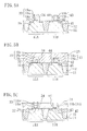
- FIGS. 4A to 4C are cross-sectional views illustrating the method for fabricating the semiconductor device according to the embodiment of the present invention in the order in which the process steps thereof are performed;
- FIGS. 5A to 5C are cross-sectional views illustrating the method for fabricating the semiconductor device according to the embodiment of the present invention in the order in which the process steps thereof are performed; and
- FIGS. 6A to 6C are cross-sectional views illustrating the method for fabricating the semiconductor device according to the embodiment of the present invention in the order in which the process steps thereof are performed.
- An embodiment of the present invention will be described with reference to the drawings. FIG. 1 shows a cross-sectional structure of a semiconductor device according to the embodiment of the present invention. As shown in FIG. 1, the semiconductor device according to the present embodiment comprises a p-channel MOS transistor and an n-channel MOS transistor which are formed on a substrate.
- In a
substrate 11 made of silicon, afirst region 11A and asecond region 11B which are isolated from each other by anisolation region 12 are formed. An n-channel MOS transistor 31 is formed in thefirst region 11A. - The n-
channel MOS transistor 31 has a firstgate insulating film 32 made of hafnium dioxide (HfO2) formed on thesubstrate 11 and afirst gate electrode 33 comprisingsidewalls 34. In the portions of thefirst region 11A which are located on both sides of thefirst gate electrode 33, n-type source/drain regions 35 are formed individually. Thefirst gate electrode 33 in the semiconductor device according to the present embodiment is a metal gate electrode comprised of ametal film 14a made of TaN and a silicide film 26a made of platinum silicide which are successively stacked in layers in an ascending order, in which themetal film 14a is formed in contact with the firstgate insulating film 32. In the present embodiment, the metal gate electrode is defined as a gate electrode formed such that a film made of a metal or a metal compound having a metallic conductivity is deposited in contact with a gate insulating film. It is assumed that the metal film in the metal gate electrode includes not only a film made of a metal but also a film made of a metal compound having a metallic conductivity. - A p-
channel MOS transistor 41 has a secondgate insulating film 42 made of HfO2 formed on thesubstrate 11 and asecond gate electrode 43 comprisingsidewalls 44. In the portions of thesecond region 11B which are located on both sides of thesecond gate electrode 43, p-type source/drain regions 45 are formed individually. Thesecond gate electrode 43 is a fully-silicided gate electrode in which asilicide film 26b is formed on the secondgate insulating film 42. The fully-silicided gate is a gate electrode formed by depositing a polysilicon film on a gate insulating film and then completely siliciding the deposited polysilicon film to the interface with the gate insulating film. - The n-
channel MOS transistor 31 and the p-channel MOS transistor 41 are covered with interlayer insulatingfilms interlayer insulating films first gate electrode 33, the n-type source/drain regions 35, thesecond gate electrode 43, and the p-type source/drain regions 45 are formed. - In the semiconductor device according to the present embodiment, the n-
channel MOS transistor 31 has thefirst gate electrode 33 which is the metal gate electrode made of TaN and the p-channel MOS transistor 41 has thesecond gate electrode 43 which is the fully-silicided gate electrode. Thus, the gate electrodes having different work functions are formed individually in the n-channel MOS transistor 31 and the p-channel MOS transistor 41. As a result, in either of the n-channel MOS transistor 31 and the p-channel MOS transistor 41, a leakage current and a threshold voltage can be reduced. - In the semiconductor device according to the present embodiment, the fully-silicided gate electrode is formed in the p-
channel MOS transistor 41. As a result, the peeling off of the gate electrode from the gate insulating film can be suppressed more reliably than in the case where a metal gate electrode using platinum (Pt) or the like is formed. In addition, the gate electrode can be formed more easily than in the case where the metal gate electrode is formed by etching Pt or the like. - Unlike in the case where the fully-silicided gate electrode is formed in each of the n-
channel MOS transistor 31 and the p-channel MOS transistor 41, full silicidation can be performed under conditions which are optimal for the p-channel MOS transistor 41. - Instead of the HfO2 film, a high dielectric constant film such as a hafnium silicate (HfSiO) film or a hafnium silicon oxynitride (HfSiON) film can be used as each of the first and second
gate insulating films gate insulating films first gate electrode 33 and allowing the obtention of a transistor with a large driving current is offered. - The
metal film 14a of thefirst gate electrode 33 may also be made of, instead of TaN, a material selected from the group consisting of tantalum (Ta), tantalum silicon (TaSi), tantalum silicon nitride (TaSiN), tantalum aluminum (TaAl), tantalum aluminum nitride (TaAIN), tantalum aluminum silicon (TaAlSi), tantalum aluminum silicon nitride (TaAlSiN), tantalum carbide (TaC), tantalum carbide nitride (TaCN), and the like. Themetal film 14a may also be a multilayer film made of at least two materials selected from the group listed above. In this case, the work function is preferably adjusted to be not less than 4.2 eV and not more than 4.5 eV. In the case where themetal film 14a is made of a nitride, the composition of nitrogen is preferably not more than 50%. - The
second gate electrode 43 may be made of, instead of platinum silicide, any of nickel silicide, cobalt silicide, and the like. - Although the semiconductor device according to the present embodiment has formed the
first gate electrode 33 by using a multilayer film of themetal film 14a and the silicide film 26a to provide easy connection between thecontact plug 28 and thefirst gate electrode 33 and reduce the resistance value of thefirst gate electrode 33, it is also possible to form thefirst gate electrode 33 by using only themetal film 14a without providing the silicide film 26a. - Referring to the drawings, a method for fabricating the semiconductor device according to the present embodiment will be described herein below. FIGS. 2A to 6C illustrate the fabrication method for the semiconductor device according to the present embodiment in the order in which the process steps thereof are performed.
- First, as shown in FIG. 2A, the
trench isolation region 12 is formed in thesubstrate 11 made of silicon so that thefirst region 11A in which the n-channel MOS transistor 31 is formed and thesecond region 11B in which the p-channel MOS transistor 41 is formed are formed. The isolation region may also be formed by using a localoxidation of silicon (LOCOS) technology. - Next, as shown in FIG. 2B, a native oxide film formed on the upper surface of the
substrate 11 is removed by using a diluted aqueous fluoric acid solution. Then, a first insulatingfilm 13 made of HfO2 or the like and serving as the firstgate insulating film 32 is formed on thesubstrate 11. - The formation of the HfO2 film may be performed appropriately by depositing a metal film made of Hf or the like by using a DC sputtering method or the like and then oxidizing the metal film. The method for depositing the metal film may also be a physical vapor deposition (PVD) method, a vacuum vapor deposition method, an electron beam deposition method, a laser deposition method, a chemical vapor deposition (CVD) method, a metal organic vapor deposition method, an atomic layer deposition method, or the like. Instead of the metal oxide film, there may also be formed a metal silicate film such as HfSiO4 film, a metal nitride-silicate film such as a HfSiON film, or the like. After the removal of the native oxide film, it is also possible to form an oxide film, a nitride film, or the like on the upper surface of the
substrate 11 as necessary. - Next, as shown in FIG. 2C, a
metal film 14 made of TaN or the like is formed by using a sputtering method or the like on the first insulatingfilm 13. In the case where themetal film 14 is made of TaN, the TaN film may be formed appropriately by sputtering a Ta target in an argon-nitrogen atmosphere under a pressure of 0.4 kPa. Ta atoms sputtered out of the Ta target adhere onto the first insulatingfilm 13 and then react with nitrogen in the atmosphere, thereby forming the TaN film. - Likewise, when the
metal film 14 is made of TaSi, TaAl, TaAlSi, TaC, or the like, the film may be formed appropriately by sputtering the corresponding metal target in an argon atmosphere or in a gas mixture of argon and nitrogen. - Next, as shown in FIG. 3A, a resist
mask 15 for exposing thesecond region 11B is formed on themetal film 14 by using a photolithographic technology. Then, the respective portions of themetal film 14 and the first insulatingfilm 13 which are formed on thesecond region 11B are etched so that the upper surface of thesubstrate 11 is exposed in thesecond region 11B. For the etching, a solution mixture of a fluoric acid and a nitric acid may be used appropriately as an etchant. Instead of wet etching, dry etching may also be used. - Next, as shown in FIG. 3B, a second insulating
film 16 is deposited over the upper surface of themetal film 14 and the exposed upper surface of thesubstrate 11. For the second insulatingfilm 16, a high dielectric constant film made of HfO2, HfSiO, HfSiON, or the like may be formed appropriately in the same manner as for the first insulatingfilm 13. The second insulatingfilm 16 may be made of a material which is the same as or different from the material of the first insulatingfilm 13. As each of the first and second insulatingfilms - The thickness of the second insulating
film 16 may be the same as that of the first insulatingfilm 13. However, as will be described later, the thickness of the first insulatingfilm 13 is preferably adjusted to be larger than that of the second insulatingfilm 16. - Next, as shown in FIG. 3C, a resist
mask 17 for exposing thefirst region 11A is formed by using a photolithographic technology. Then, the portion of the second insulatingfilm 16 which is formed on themetal film 14 is removed. The removal of the portion of the second insulatingfilm 16 may be performed appropriately by wet etching using, e.g., a diluted fluoric acid as an etchant. When a protective film made of polysilicon is formed on the second insulatingfilm 16, wet etching may be performed appropriately by using a diluted fluoric acid after the protective film is removed first by using an APM solution (a solution mixture of ammonia, aqueous hydrogen peroxide, and water). Instead of wet etching, dry etching may also be used. - The present embodiment has removed the first insulating
film 13 and themetal film 14 from thesecond region 11B in order to prevent the degradation of the quality of the gate insulating film of the p-channel MOS transistor 41. However, it is also possible to leave the first insulatingfilm 13 as it is in thesecond region 11B and use it as a replacement for the second insulatingfilm 16. In this case, the merit of allowing the omission of the step of forming the second insulatingfilm 16 and thereby allowing the simplification of the steps is offered. - Next, as shown in FIG. 4A, a
polysilicon film 18 and a third insulatingfilm 19 made of SiO2 or the like are deposited over the respective upper surfaces of themetal film 14 and the second insulatingfilm 16. The deposition of thepolysilicon film 18 may be performed appropriately by a CVD method using a silane gas. The deposition of the third insulatingfilm 19 may be performed appropriately by a plasma CVD method using tetraethoxysilane (TEOS). The thirdinsulating film 19 is a protective film in the silicidation of the source/drain regions, which will be described later, and may be formed appropriately as necessary. Subsequently, a resistmask 20 is formed on each of portions serving as the first andsecond gate electrodes - Next, as shown in FIG. 4B, the third insulating
film 19, thepolysilicon film 18, themetal film 14, the first insulatingfilm 13, and the second insulatingfilm 16 are selectively removed by dry etching so that thefirst gate electrode 33 comprised of themetal film 14a, apolysilicon film 18a, and a thirdinsulating film 19a and thesecond gate electrode 43 made of apolysilicon film 18b and a thirdinsulating film 19b are formed. Thereafter, an n-type impurity is implanted into thefirst region 11A and a p-type impurity is implanted into thesecond region 11B, each by using an ion implantation technology, so that extension regions (not shown) are formed individually. - Next, as shown in FIG. 4C, a SiN film is deposited over the entire surface of the
substrate 11 and then subjected to anisotropic etching so that thesidewalls 34 and thesidewalls 44 are formed on the respective side surfaces of the first andsecond gate electrodes - Next, as shown in FIG. 5A, an n-type impurity is implanted into the
first region 11A and a p-type impurity is implanted into thesecond region 11B and a thermal process is performed at 1000 °C for 3 seconds, thereby individually forming the n-type source/drain regions 35 and the p-type source/drain regions 45. - Subsequently, a
metal film 23 made of nickel is deposited over the entire surface of thesubstrate 11 and then subjected to a thermal process at a temperature of 500 °C so that the n-type source/drain regions 35 and the p-type source/drain regions 45 are silicided. Since thepolysilicon film 18a of thefirst gate electrode 33 and thepolysilicon film 18b of thesecond gate electrode 43 are protected by the third insulatingfilms metal film 23, platinum, cobalt, or the like may also be used. - Next, as shown in FIG. 5B, the unreacted portion of the
metal film 23 is removed by using a SPM solution (a solution mixture of a sulfuric acid, aqueous hydrogen peroxide, and water). Thereafter, aninterlayer insulating film 24 is deposited over the entire surface of thesubstrate 11. Subsequently, theinterlayer insulating film 24 is polished by using a CMP technology till the thirdinsulating film 19a of thefirst gate electrode 33 and the thirdinsulating film 19b of thesecond gate electrode 43 are exposed. - Next, as shown in FIG. 5C, the third insulating
films polysilicon film 18a of thefirst gate electrode 33 and thepolysilicon film 18b of thesecond gate electrode 43 are exposed. - Next, as shown in FIG. 6A, a
metal film 25 made of platinum is deposited by a sputtering method or the like over the entire surface of thesubstrate 11. As the deposition method, CVD, vapor deposition, laser abrasion, or the like may also be used. Instead of platinum, there may also be deposited nickel, cobalt, or the like. - Next, as shown in FIG. 6B, a thermal process is performed at a temperature of not more than 500 °C, thereby individually changing the
polysilicon film 18a of thefirst gate electrode 33 and thepolysilicon film 18b of thesecond gate electrode 43 into thesilicide films 26a and 26b each made of platinum silicide. In this case, in the p-channel MOS transistor 41, a stress in a direction of compression is applied to the secondgate insulating film 42 as a result of volume expansion when thepolysilicon film 18b is changed into thesilicide film 26b. Since the mobility of hole carriers is normally improved by the compressive stress, the characteristics of a drain current in the p-channel MOS transistor 41 are improved. In the n-channel MOS transistor 31, on the other hand, when the stress in the direction of compression is applied to the firstgate insulating film 32, the characteristics are degraded conversely to the case where the stress is applied in the p-channel MOS transistor. However, since themetal film 14a is present between the silicide film 26a and the firstgate insulating film 32 in the n-channel MOS transistor 31, the effect of the stress is suppressed and the degradation of the characteristics thereof is limited. - Next, as shown in FIG. 6C, the unreacted portion of the
metal film 25 is removed by using a SPM solution. Then, aninterlayer insulating film 27 is deposited to form the contact plugs 28 electrically connected individually to the n-type source/drain regions 35, the p-type source/drain regions 45, thefirst gate electrode 33, and thesecond gate electrode 43, each of which has been silicided. - When a high dielectric constant material is used for a gate insulating film, a SiO2 film is relatively easily formed at the interface between silicon and the high dielectric constant film so that the gate insulating film has a multilayer structure of the thin SiO2 film and the high dielectric constant film. The upper-layer dielectric film has a small band gap and a large thickness, while the lower-layer SiO2 film has a large band gap and a small thickness. In the gate insulating film having such an asymmetrical band structure, the magnitude of a leakage current differs depending on the direction of carrier injection. Therefore, it follows that, in an n-channel MOS transistor and a p-channel MOS transistor, the leakage currents have different characteristics.
- In the n-channel MOS transistor, electrons supplied from the source/drain regions are introduced from the channel side so that the leakage current is primarily determined by the thickness of the SiO2 film in contact with the channel. Since the SiO2 film is normally thinner than the high dielectric constant film, the leakage current is large and larger than in the p-channel MOS transistor. Accordingly, to suppress the leakage current in the n-channel MOS transistor, it is required to form the gate insulating film made of a high dielectric constant material such that it is thicker than in the p-channel MOS transistor.
- In the present embodiment, the first
gate insulating film 32 of the n-channel MOS transistor 31 and the secondgate insulating film 42 of the p-channel MOS transistor 41 are formed by different process steps. This allows easy formation the firstgate insulating film 32 which is thicker than the secondgate insulating film 42 and therefore allows the respective leakage currents of the n-channel MOS transistor 31 and the p-channel MOS transistor 41 to have equal characteristics. - Thus, the semiconductor device according to the present invention and the fabrication method therefor can implement a semiconductor device in which an n-channel MOS transistor and a p-channel MOS transistor, each of which has a low leakage current and a low threshold voltage, are formed in a single substrate and are therefore useful as a semiconductor device comprising an n-channel MOS transistor and a p-channel MOS transistor, a fabrication method therefor, and the like.
Claims (12)
- A semiconductor device comprising:a transistor of a first conductivity formed on a semiconductor substrate and having a first gate insulating film and a first gate electrode; anda transistor of a second conductivity type formed on a different region of the semiconductor substrate from a region thereof on which the transistor of the first conductivity is formed and having a second gate insulating film and a second gate electrode, whereinthe first gate electrode is a metal gate electrode having a metal film andthe second gate electrode is a fully-silicided gate electrode.
- The semiconductor device of claim 1, wherein at least one of the first gate insulating film and the second gate insulating film is made of a high dielectric constant material.
- The semiconductor device of claim 2, wherein the high dielectric constant material contains at least one of silicon, hafnium, zirconium, titanium, tantalum, aluminum, and a rare earth metal.
- The semiconductor device of claim 1, wherein the transistor of the first conductivity type is an n-channel MOS transistor and the transistor of the second conductivity type is a p-channel MOS transistor.
- The semiconductor device of claim 4, wherein the metal film is a single-layer film made of a material selected from the group consisting of Ta, TaN, TaSi, TaSiN, TaAl, TaAlN, TaAlSi, TaAlSiN, TaC, and TaCN or a multilayer film made of at least two materials selected from the group consisting of Ta, TaN, TaSi, TaSiN, TaAl, TaAlN, TaAlSi, TaAlSiN, TaC, and TaCN.
- The semiconductor device of claim 5, wherein the metal gate electrode has a silicide film formed on the metal film.
- The semiconductor device of claim 4, wherein the first gate insulating film has a thickness larger than a thickness of the second gate insulating film.
- The semiconductor device of claim 1, wherein the fully-silicided gate electrode is made of a silicide containing any one ofNi, Pt, and Co.
- A method for fabricating a semiconductor device, the method comprising the steps of:(a) forming a first insulating film on a semiconductor substrate and then forming a metal film on the formed first insulating film;(b) removing respective portions of the first insulating film and the metal film which are located in a region of the semiconductor substrate to expose an upper surface of the semiconductor substrate;(c) forming a second insulating film on the exposed portion of the semiconductor substrate;(d) forming a polysilicon film over the metal film and the second insulating film;(e) patterning the polysilicon film formed on the metal film and the metal film to form a first gate electrode which is a metal gate electrode and patterning the polysilicon film formed on the second insulating film to form a second gate electrode; and(f) siliciding the patterned polysilicon film to change the second gate electrode into a fully-silicided gate electrode.
- The method of claim 9, wherein the step (c) includes the sub-steps of:forming the second insulating film over the exposed portion of the semiconductor substrate and the metal film; andremoving the portion of the second insulating film which is formed on the metal film.
- The method of claim 9, further comprising the step of:(g) after the step (e) and before the step (f), forming sidewalls on respective side surfaces of the first gate electrode and the second gate electrode.
- The method of claim 11, further comprising the steps of:(h) after the step (g) and before the step (f), forming source/drain regions of a first conductivity type in respective portions of the semiconductor substrate which are located on both sides of the first gate electrode and forming source/drain regions of a second conductivity type in respective portions of the semiconductor substrate which are located on both sides of the second gate electrode;(i) after the step (h) and before the step (f), siliciding the source/drain regions of the first conductivity type and the source/drain regions of the second conductivity type;(j) after the step (d) and before the step (i), forming a third insulating film on the polysilicon film; and(k) after the step (j) and before the step (f), removing the third insulating film.
Applications Claiming Priority (1)
| Application Number | Priority Date | Filing Date | Title |
|---|---|---|---|
| JP2006116591A JP2007288096A (en) | 2006-04-20 | 2006-04-20 | Semiconductor device and manufacturing method thereof |
Publications (2)
| Publication Number | Publication Date |
|---|---|
| EP1848033A2 true EP1848033A2 (en) | 2007-10-24 |
| EP1848033A3 EP1848033A3 (en) | 2009-04-08 |
Family
ID=38226410
Family Applications (1)
| Application Number | Title | Priority Date | Filing Date |
|---|---|---|---|
| EP07105228A Withdrawn EP1848033A3 (en) | 2006-04-20 | 2007-03-29 | Semiconductor Device and Fabrication Method Therefor |
Country Status (3)
| Country | Link |
|---|---|
| US (1) | US20070284670A1 (en) |
| EP (1) | EP1848033A3 (en) |
| JP (1) | JP2007288096A (en) |
Cited By (1)
| Publication number | Priority date | Publication date | Assignee | Title |
|---|---|---|---|---|
| US7790624B2 (en) | 2008-07-16 | 2010-09-07 | Global Foundries Inc. | Methods for removing a metal-comprising material from a semiconductor substrate |
Families Citing this family (11)
| Publication number | Priority date | Publication date | Assignee | Title |
|---|---|---|---|---|
| JP2007123548A (en) * | 2005-10-28 | 2007-05-17 | Renesas Technology Corp | Manufacturing method of semiconductor device |
| US7678298B2 (en) | 2007-09-25 | 2010-03-16 | Applied Materials, Inc. | Tantalum carbide nitride materials by vapor deposition processes |
| US7585762B2 (en) * | 2007-09-25 | 2009-09-08 | Applied Materials, Inc. | Vapor deposition processes for tantalum carbide nitride materials |
| JP5190250B2 (en) * | 2007-11-02 | 2013-04-24 | パナソニック株式会社 | Semiconductor device |
| FR2928029B1 (en) * | 2008-02-27 | 2011-04-08 | St Microelectronics Crolles 2 | METHOD FOR MANUFACTURING A BENT GRID SEMICONDUCTOR DEVICE AND CORRESPONDING INTEGRATED CIRCUIT |
| JP5147471B2 (en) * | 2008-03-13 | 2013-02-20 | パナソニック株式会社 | Semiconductor device |
| JP5291992B2 (en) * | 2008-06-10 | 2013-09-18 | ルネサスエレクトロニクス株式会社 | Manufacturing method of semiconductor device |
| JP2010027638A (en) * | 2008-07-15 | 2010-02-04 | Sumitomo Electric Ind Ltd | Fabrication process of semiconductor device and semiconductor device |
| JP2012059888A (en) * | 2010-09-08 | 2012-03-22 | Renesas Electronics Corp | Semiconductor device and method of manufacturing the same |
| JP5816539B2 (en) | 2011-12-05 | 2015-11-18 | ルネサスエレクトロニクス株式会社 | Semiconductor device and manufacturing method thereof |
| CN112823408A (en) * | 2018-10-08 | 2021-05-18 | 应用材料公司 | Method and apparatus for N-type metal oxide semiconductor (NMOS) metal gate material for Atomic Layer Deposition (ALD) processes using metal-based precursors |
Family Cites Families (4)
| Publication number | Priority date | Publication date | Assignee | Title |
|---|---|---|---|---|
| US6383879B1 (en) * | 1999-12-03 | 2002-05-07 | Agere Systems Guardian Corp. | Semiconductor device having a metal gate with a work function compatible with a semiconductor device |
| US6686298B1 (en) * | 2000-06-22 | 2004-02-03 | Micron Technology, Inc. | Methods of forming structures over semiconductor substrates, and methods of forming transistors associated with semiconductor substrates |
| US6475908B1 (en) * | 2001-10-18 | 2002-11-05 | Chartered Semiconductor Manufacturing Ltd. | Dual metal gate process: metals and their silicides |
| JP4163164B2 (en) * | 2004-09-07 | 2008-10-08 | 株式会社ルネサステクノロジ | Semiconductor device and manufacturing method thereof |
-
2006
- 2006-04-20 JP JP2006116591A patent/JP2007288096A/en active Pending
-
2007
- 2007-03-08 US US11/715,437 patent/US20070284670A1/en not_active Abandoned
- 2007-03-29 EP EP07105228A patent/EP1848033A3/en not_active Withdrawn
Cited By (1)
| Publication number | Priority date | Publication date | Assignee | Title |
|---|---|---|---|---|
| US7790624B2 (en) | 2008-07-16 | 2010-09-07 | Global Foundries Inc. | Methods for removing a metal-comprising material from a semiconductor substrate |
Also Published As
| Publication number | Publication date |
|---|---|
| US20070284670A1 (en) | 2007-12-13 |
| EP1848033A3 (en) | 2009-04-08 |
| JP2007288096A (en) | 2007-11-01 |
Similar Documents
| Publication | Publication Date | Title |
|---|---|---|
| US20070284670A1 (en) | Semiconductor device and fabrication method therefor | |
| US7229873B2 (en) | Process for manufacturing dual work function metal gates in a microelectronics device | |
| US7947591B2 (en) | Semiconductor devices with dual-metal gate structures and fabrication methods thereof | |
| US8034678B2 (en) | Complementary metal oxide semiconductor device fabrication method | |
| US9673326B2 (en) | Metal oxide semiconductor having epitaxial source drain regions and a method of manufacturing same using dummy gate process | |
| US7084024B2 (en) | Gate electrode forming methods using conductive hard mask | |
| US7183596B2 (en) | Composite gate structure in an integrated circuit | |
| US8658489B2 (en) | Method for dual work function metal gate CMOS with selective capping | |
| US8026539B2 (en) | Metal oxide semiconductor devices having doped silicon-compromising capping layers and methods for fabricating the same | |
| JP5569173B2 (en) | Semiconductor device manufacturing method and semiconductor device | |
| CN101233611A (en) | Metal-gate MOSFETs transitioned through an all-semiconducting metal alloy | |
| US7319258B2 (en) | Semiconductor-on-insulator chip with<100>-oriented transistors | |
| US20090020824A1 (en) | Semiconductor device and method for producing the same | |
| US20100213555A1 (en) | Metal oxide semiconductor devices having capping layers and methods for fabricating the same | |
| EP1732133A2 (en) | Semiconductor device and method for fabricating the same | |
| US8575014B2 (en) | Semiconductor device fabricated using a metal microstructure control process | |
| JP2008117963A (en) | Field effect transistor, semiconductor device, and manufacturing method thereof | |
| US9960162B2 (en) | Hybrid high-k first and high-k last replacement gate process | |
| US20060051915A1 (en) | Semiconductor device and manufacturing method thereof | |
| US7666774B2 (en) | CMOS structure including dual metal containing composite gates | |
| TWI509702B (en) | Metal gate transistor and method for fabricating the same | |
| TWI478244B (en) | Metal oxide semiconductor devices having doped silicon-comprising capping layers and methods for fabricating the same | |
| JP2007287793A (en) | Manufacturing method of semiconductor device | |
| US20100068861A1 (en) | Method of defining gate structure height for semiconductor devices |
Legal Events
| Date | Code | Title | Description |
|---|---|---|---|
| PUAI | Public reference made under article 153(3) epc to a published international application that has entered the european phase |
Free format text: ORIGINAL CODE: 0009012 |
|
| AK | Designated contracting states |
Kind code of ref document: A2 Designated state(s): AT BE BG CH CY CZ DE DK EE ES FI FR GB GR HU IE IS IT LI LT LU LV MC MT NL PL PT RO SE SI SK TR |
|
| AX | Request for extension of the european patent |
Extension state: AL BA HR MK YU |
|
| RAP1 | Party data changed (applicant data changed or rights of an application transferred) |
Owner name: INTERUNIVERSITAIR MICROELEKTRONICA CENTRUM VZW Owner name: PANASONIC CORPORATION |
|
| PUAL | Search report despatched |
Free format text: ORIGINAL CODE: 0009013 |
|
| AK | Designated contracting states |
Kind code of ref document: A3 Designated state(s): AT BE BG CH CY CZ DE DK EE ES FI FR GB GR HU IE IS IT LI LT LU LV MC MT NL PL PT RO SE SI SK TR |
|
| AX | Request for extension of the european patent |
Extension state: AL BA HR MK RS |
|
| RAP1 | Party data changed (applicant data changed or rights of an application transferred) |
Owner name: IMEC Owner name: PANASONIC CORPORATION |
|
| AKX | Designation fees paid | ||
| STAA | Information on the status of an ep patent application or granted ep patent |
Free format text: STATUS: THE APPLICATION IS DEEMED TO BE WITHDRAWN |
|
| 18D | Application deemed to be withdrawn |
Effective date: 20091009 |
|
| REG | Reference to a national code |
Ref country code: DE Ref legal event code: 8566 |