EP1845757A2 - Liquid crystal television and backlight power supplying circuit - Google Patents
Liquid crystal television and backlight power supplying circuit Download PDFInfo
- Publication number
- EP1845757A2 EP1845757A2 EP07007439A EP07007439A EP1845757A2 EP 1845757 A2 EP1845757 A2 EP 1845757A2 EP 07007439 A EP07007439 A EP 07007439A EP 07007439 A EP07007439 A EP 07007439A EP 1845757 A2 EP1845757 A2 EP 1845757A2
- Authority
- EP
- European Patent Office
- Prior art keywords
- circuit
- power supply
- voltage
- supply voltage
- driving signal
- Prior art date
- Legal status (The legal status is an assumption and is not a legal conclusion. Google has not performed a legal analysis and makes no representation as to the accuracy of the status listed.)
- Withdrawn
Links
- 239000004973 liquid crystal related substance Substances 0.000 title claims description 31
- 230000001681 protective effect Effects 0.000 claims abstract description 40
- 238000011084 recovery Methods 0.000 claims abstract description 24
- 230000009993 protective function Effects 0.000 claims abstract description 15
- 239000000758 substrate Substances 0.000 description 16
- 230000006870 function Effects 0.000 description 12
- 230000015556 catabolic process Effects 0.000 description 5
- 238000010586 diagram Methods 0.000 description 4
- 239000000463 material Substances 0.000 description 3
- 238000000034 method Methods 0.000 description 3
- 241001270131 Agaricus moelleri Species 0.000 description 2
- 230000006698 induction Effects 0.000 description 2
- 239000011159 matrix material Substances 0.000 description 2
- 230000004044 response Effects 0.000 description 2
- 238000004804 winding Methods 0.000 description 2
- 230000005856 abnormality Effects 0.000 description 1
- 230000009471 action Effects 0.000 description 1
- 230000003321 amplification Effects 0.000 description 1
- 230000008859 change Effects 0.000 description 1
- 239000013078 crystal Substances 0.000 description 1
- 238000002955 isolation Methods 0.000 description 1
- 230000007257 malfunction Effects 0.000 description 1
- 238000003199 nucleic acid amplification method Methods 0.000 description 1
- 230000009467 reduction Effects 0.000 description 1
- 238000002834 transmittance Methods 0.000 description 1
Images




Classifications
-
- H—ELECTRICITY
- H05—ELECTRIC TECHNIQUES NOT OTHERWISE PROVIDED FOR
- H05B—ELECTRIC HEATING; ELECTRIC LIGHT SOURCES NOT OTHERWISE PROVIDED FOR; CIRCUIT ARRANGEMENTS FOR ELECTRIC LIGHT SOURCES, IN GENERAL
- H05B41/00—Circuit arrangements or apparatus for igniting or operating discharge lamps
- H05B41/14—Circuit arrangements
- H05B41/26—Circuit arrangements in which the lamp is fed by power derived from DC by means of a converter, e.g. by high-voltage DC
- H05B41/28—Circuit arrangements in which the lamp is fed by power derived from DC by means of a converter, e.g. by high-voltage DC using static converters
- H05B41/282—Circuit arrangements in which the lamp is fed by power derived from DC by means of a converter, e.g. by high-voltage DC using static converters with semiconductor devices
- H05B41/285—Arrangements for protecting lamps or circuits against abnormal operating conditions
- H05B41/2851—Arrangements for protecting lamps or circuits against abnormal operating conditions for protecting the circuit against abnormal operating conditions
- H05B41/2853—Arrangements for protecting lamps or circuits against abnormal operating conditions for protecting the circuit against abnormal operating conditions against abnormal power supply conditions
-
- G—PHYSICS
- G09—EDUCATION; CRYPTOGRAPHY; DISPLAY; ADVERTISING; SEALS
- G09G—ARRANGEMENTS OR CIRCUITS FOR CONTROL OF INDICATING DEVICES USING STATIC MEANS TO PRESENT VARIABLE INFORMATION
- G09G3/00—Control arrangements or circuits, of interest only in connection with visual indicators other than cathode-ray tubes
- G09G3/20—Control arrangements or circuits, of interest only in connection with visual indicators other than cathode-ray tubes for presentation of an assembly of a number of characters, e.g. a page, by composing the assembly by combination of individual elements arranged in a matrix no fixed position being assigned to or needed to be assigned to the individual characters or partial characters
- G09G3/34—Control arrangements or circuits, of interest only in connection with visual indicators other than cathode-ray tubes for presentation of an assembly of a number of characters, e.g. a page, by composing the assembly by combination of individual elements arranged in a matrix no fixed position being assigned to or needed to be assigned to the individual characters or partial characters by control of light from an independent source
- G09G3/3406—Control of illumination source
-
- G—PHYSICS
- G09—EDUCATION; CRYPTOGRAPHY; DISPLAY; ADVERTISING; SEALS
- G09G—ARRANGEMENTS OR CIRCUITS FOR CONTROL OF INDICATING DEVICES USING STATIC MEANS TO PRESENT VARIABLE INFORMATION
- G09G2330/00—Aspects of power supply; Aspects of display protection and defect management
- G09G2330/02—Details of power systems and of start or stop of display operation
-
- G—PHYSICS
- G09—EDUCATION; CRYPTOGRAPHY; DISPLAY; ADVERTISING; SEALS
- G09G—ARRANGEMENTS OR CIRCUITS FOR CONTROL OF INDICATING DEVICES USING STATIC MEANS TO PRESENT VARIABLE INFORMATION
- G09G2330/00—Aspects of power supply; Aspects of display protection and defect management
- G09G2330/04—Display protection
-
- Y—GENERAL TAGGING OF NEW TECHNOLOGICAL DEVELOPMENTS; GENERAL TAGGING OF CROSS-SECTIONAL TECHNOLOGIES SPANNING OVER SEVERAL SECTIONS OF THE IPC; TECHNICAL SUBJECTS COVERED BY FORMER USPC CROSS-REFERENCE ART COLLECTIONS [XRACs] AND DIGESTS
- Y02—TECHNOLOGIES OR APPLICATIONS FOR MITIGATION OR ADAPTATION AGAINST CLIMATE CHANGE
- Y02B—CLIMATE CHANGE MITIGATION TECHNOLOGIES RELATED TO BUILDINGS, e.g. HOUSING, HOUSE APPLIANCES OR RELATED END-USER APPLICATIONS
- Y02B20/00—Energy efficient lighting technologies, e.g. halogen lamps or gas discharge lamps
Definitions
- the present invention relates to a backlight power supplying circuit for supplying power to a backlight.
- the invention relates to a backlight power supplying circuit having a function of protecting the circuit against voltage drop, and to a liquid crystal television (TV) with use of the backlight power supplying circuit.
- TV liquid crystal television
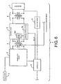
- Fig. 6 shows a conventional backlight power supplying circuit.
- a backlight power supplying circuit 1 includes a main power supply circuit 3, a main transformer 4, an inverter circuit 5, a transformer 6, a control unit 8, and a determining circuit 9.
- the main power supply circuit 3 rectifies and reduces a voltage of a commercially available 100V AC power supply, which is input from a plug socket 2, and the voltage is divided at the main transformer 4 to thereby supply power to the inverter circuit 5. Further, the main transformer 4 supplies power to various circuits other than the inverter circuit 5.
- the inverter circuit 5 is intended to increase the voltage divided through the main transformer 4 due to the switching action of a MOSFET etc. up to an output voltage level necessary for the backlight 7.
- Such MOSFETs execute a switching function behind the control of the inverter controlling IC 5a incorporated into the inverter circuit 5.
- the control unit 8 controls driving of the main power supply circuit 3 and the inverter circuit 5.
- the control unit 8 starts driving the main power supply circuit 3 and sends a signal BL_on that triggers the inverter controlling IC 5a to execute the switching function.
- the inverter circuit 5 boosts the power supply voltage input through the main transformer 4 and outputs the boosted voltage to the backlight 7 through the transformer 6.
- a secondary coil of the transformer 6 makes determination about the output voltage for the backlight by means of the determining circuit 9. If the determining circuit 9 detects any abnormality in output voltage, a feedback signal is sent to the control unit 8.
- the control unit 8 receives the feedback signal to control the power supply of the main power supply circuit 3.
- the inverter controlling IC 5a stops driving the inverter circuit 5 without recognizing the signal BL_on.
- the inverter controlling IC includes, as a protective functional unit, a protective circuit 5al that stops driving the inverter circuit 5 when a voltage level of the signal BL_on is lowered.
- the protective circuit Since the output voltage generated with the inverter circuit 5 is abnormally as high as 1000 V, the protective circuit temporarily cuts off the supply of the signal BL_on from the control unit 8 (cuts off a main power supply) to thereby prevent the backlight 7 from being damaged due to malfunction of the inverter circuit 5. Hence, upon such temporary blackout, a user needs to turn on the main power supply again to redrive the liquid crystal TV
- Japanese Unexamined Patent Application Publication No. 2004-355865 discloses a technique using a switch and control circuit for resetting a latch state if a controlling IC for controlling a main power supply circuit is shifted to the latch state due to temporary blackout.
- Japanese Unexamined Patent Application Publication No. 2004-355865 has the following problem. That is, the publication does not contain any reference to an inverter circuit supplied with power from the main power supply circuit through a main transformer. Thus, in the configuration including a controlling IC on the inverter side as well as on the main power supply circuit side, it is necessary to take a countermeasure against the temporary blackout for the inverter controlling IC on the inverter side.
- the present invention aims at providing a liquid crystal TV with use of an inverter-circuit power supply circuit for supplying power to an inverter circuit supplied with a power supply voltage from a main power supply circuit through a main transformer and having a protective function of temporarily cutting off a backlight driving signal to thereby redrive the inverter circuit especially when the power supply voltage becomes lower than a specified voltage to stop the inverter circuit.
- the inverter-circuit power supply circuit can redrive the inverter circuit without turning on a main power again upon temporary blackout.
- a liquid crystal television comprising:
- the inverter circuit applies an output voltage to the backlight based on DC power supplied from the main power supply circuit
- the protective circuit of the inverter controlling IC has a protective function of stopping boosting if the power supply voltage from the main power supply circuit is lower than a specified value due to temporary blackout.
- the protective function of the protective circuit can be cancelled by temporarily cutting off the backlight driving signal.
- the inverter circuit includes the power recovery circuit to cancel the protective function of the protective circuit upon temporary blackout. If the power supply voltage from the main power supply circuit lowers due to temporary blackout, the power recovery circuit temporarily cuts off the backlight driving signal from the microcomputer and restarts the supply of the signal to the protective circuit when the power supply voltage is increased up to the specified voltage or higher.
- the power recovery circuit includes the power supply voltage determining circuit, the backlight driving signal cutoff circuit, and the switchover circuit, and executes ON/OFF control over a backlight driving voltage from the microcomputer based on the power supply voltage from the main power supply circuit.
- a backlight power supplying circuit includes:
- the inverter circuit applies an output voltage to the backlight based on DC power supplied from the main power supply circuit
- the protective circuit of the inverter controlling IC has a protective function of stopping boosting if the power supply voltage from the main power supply circuit is lower than a specified value due to temporary blackout.
- the protective function of the protective circuit can be cancelled by temporarily cutting off the backlight driving signal.
- the inverter circuit includes the power recovery circuit to cancel the protective function of the protective circuit upon temporary blackout. If the power supply voltage from the main power supply circuit lowers due to temporary blackout, the power recovery circuit temporarily cuts off the backlight driving signal from the microcomputer and restarts the supply of the signal to the protective circuit when the power supply voltage is increased up to the specified voltage or higher.
- the power recovery circuit includes the power supply voltage determining circuit, the backlight driving signal cutoff circuit, and the switchover circuit, and executes ON/OFF control over a backlight driving voltage from the microcomputer based on the power supply voltage from the main power supply circuit.
- an inverter-circuit power supply circuit for supplying power to an inverter circuit having a protective function of temporarily cutting off a backlight driving signal to thereby redrive the inverter circuit especially when the power supply voltage becomes lower than a specified voltage to stop the inverter circuit.
- the inverter-circuit power supply circuit can redrive the inverter circuit without turning on a main power again upon temporary blackout.
- the power supply voltage determining circuit determines whether or not the power supply voltage is not lower than a specified voltage by use of a Zener diode,
- the backlight driving signal cutoff circuit outputs the supply voltage outputted from the main power circuit to the base of a transistor, the backlight driving signal outputted from the control unit is emitted to a ground through an emitter from the collector of the transistor, and when the determination current is outputted, the switchover circuit turns on the backlight driving signal which is intercepting the supply voltage being outputted to the base of the transistor, and is outputted to the protection circuit.
- the power supply voltage determining circuit compares the power supply voltage with the specified voltage by use of a Zener diode. Further, the backlight driving signal cutoff circuit switchingly connects/disconnects between the collector and emitter of the second transistor based on the power supply voltage to thereby emit the backlight driving signal from the control unit to the ground terminal.
- the switchover circuit outputs a determination current from the power supply voltage determining circuit to the base of the first transistor to thereby control the second transistor to emit the backlight driving signal to the ground terminal.
- the power recovery circuit can be configured by any available Zener diode or transistor, so the circuit configuration costs low
- the specified voltage can be changed by replacing the Zener diode, and conditions of the power recovery circuit can be easily changed.
- the protective circuit is realized based on control logic of the inverter controlling IC.
- the protective circuit may be realized based on control logic of the inverter controlling IC.
- the present invention is applicable to an inverter controlling IC incorporating a protective circuit.
- a backlight power supplying circuit according to the present invention will be described in detail below based on a liquid crystal TV including the backlight power supplying circuit.
- embodiments of the present invention will be described in the following order.
- Fig. 1 is a block diagram of the liquid crystal TV 10 of this device.
- the liquid crystal TV 10 includes a display device 15 including a digital substrate 11, an analog substrate 12, a liquid crystal display 13, and a speaker 14, and a remote controller 16. Functions of each part are described next.
- a tuner unit 11a On the digital substrate 11, a tuner unit 11a, a video circuit 11b, a voice circuit 11c, and a control unit 11d are formed. As shown in Fig. 1, the components of the digital substrate 11 are connected to the control unit 11d through a bus 11e, and execute their functions under the control of the control unit 11d.
- the control unit 11d includes a microcomputer 11d2 as a control center, a recording unit 11d3 such as a ROM or RAM, and an infrared receiving/converting unit 11d1 receiving an actuating signal from the remote controller 16.
- an infrared transmitter unit 16a transmits an infrared signal to an infrared receiving/converting unit 11d1, and then the infrared receiving/converting unit 11d1 converts the received infrared signal into an actuating signal of a predetermined voltage level to output the signal to the microcomputer 11d2.
- the microcomputer 11d2 outputs control signals to each component on the digital substrate 11 through the bus 11e based on control programs recorded on the recording unit 11d3.
- the tuner unit 11a selects only a specific frequency band of airwaves received by an antenna 11a1 to adjust chroma based on the airwaves of the selected specific frequency band to generate a video signal and a voice signal.
- the generated video signal is sent to the video circuit 11b, and the voice signal is sent to the voice circuit 11c.
- the tuner unit 11a of this device may receive analog broadcasting based on a PLL method, both analog broadcasting and digital broadcasting, or only digital broadcasting.
- the video circuit 11b receives the generated video signal to generate RGB signals corresponding to RGB gray scales for displaying a screen and perform predetermined signal processing on the generated RGB signals. Further, the video circuit 11b decomposes the RGB signals in accordance with the number of pixels of a liquid crystal panel 13b as described later and then outputs the signals to the liquid crystal panel 13b.
- the voice circuit 11c receives the generated voice signal and performs signal processing such as amplification on the voice signal based on a control signal from the control unit 11d.
- the voice signal subjected to the signal processing is sent to the speaker 14 and output as voice afterward.
- the liquid crystal display 13 includes the liquid crystal panel 13b having pixels of liquid crystal material arranged in matrix, a driver circuit 13a for applying a driving voltage to the liquid crystal panel 13b, and a backlight 13c for illuminating the liquid crystal panel 13b from the back.
- the driver circuit 13a applies a driving voltage as an applied voltage to predetermined pixels of the liquid crystal panel 13b on the row basis, based on the RGB signals that are divided for each pixel of the liquid crystal panel 13b by the video circuit 11b.
- pixels of liquid crystal material are arranged in matrix; the orientation of crystal grains of the liquid crystal material is changed in accordance with the driving voltage.
- Such pixels include a set of three pixels corresponding to RGB.
- the backlight 13c illuminates the liquid crystal panel 13b from the back.
- the backlight 13c serves as a light source for light transmitted through pixels.
- a fluorescent tube used for the backlight 13c a cold-cathode tube can be used.
- the tube may be a U-shaped tube, a straight tube, or a pseudo U-shaped tube.
- the analog substrate 12 supplies power necessary for the above digital substrate 11 or liquid crystal display 13.
- the substrate 12 rectifies commercially available 100-volt power, followed by isolation with the transformer. Then, the substrate 12 outputs the power to each DC/DC converter side. On the DC/DC converter side, a voltage is boosted or reduced to thereby generate and supply a stabilized AC power to the digital substrate 11 or the liquid crystal display 13.
- Fig. 2 is a block diagram of the analog substrate 12.
- the analog substrate 12 includes a main power supply circuit 12a, a main transformer 12b, an inverter circuit 12c, a transformer 12d, a detecting circuit 12f, and a feedback control circuit 12e.
- plural DC/DC converters that generate a predetermined AC power based on the power supplied from the main power supply circuit 12a through the main transformer 12b, but the present invention relates to the inverter circuit 12c, so description about the converters is omitted here.
- a function of the analog substrate 12 is described below.
- the main power supply circuit 12a converts the commercially available 100V AC power supplied from the plug socket 12g into a DC power after full-wave rectification, and then applies the DC power to the primary coil 12b1 of the main transformer 12b.
- a rectifying function of the main power supply circuit 12a of the present invention is realized by a bridge circuit including a diode or the like.
- a secondary coil 12b2 having a winding ratio different from that of the primary coil 12b1 is provided on the opposite side of the primary coil 12b1 of the main transformer 12b, and an electromotive force is generated on the secondary coil 12b2 due to mutual induction. Further, the electromotive force generated on the secondary coil 12b2 is applied to the inverter circuit 12c or each DC/DC converter (not shown) through voltage division.
- the inverter circuit 12c boosts a voltage with the switching circuit 12c2 based on the voltage applied by the secondary coil 12b2.
- the switching circuit 12c2 is composed of four MOSFETs, and the inverter controlling IC12cl controls the four MOSFETs to thereby generate an AC power having positive half cycle and negative half cycle of sine waves based on the DC power.
- the inverter circuit 12c incorporates the protective circuit 17 and a power recovery circuit 12c3 as described below. Provided that the power supply voltage of the secondary coil 12b2 is lower than the specified voltage, and the inverter circuit 12c is stopped, the protective circuit 17 has a protective function of temporarily cutting off the supply of the backlight driving signal from the microcomputer 11d2 to redrive the inverter circuit.
- the switching circuit 12c2 is driven by applying a divided one of the voltage value of the secondary coil 12b2 to the inverter controlling IC12cl and applying a signal BL_on as a backlight driving signal output from the microcomputer 11d2 of the digital substrate 11 to the protective circuit 17.
- a voltage of 24 volts generated with the main transformer 12b is divided, and the divided voltage of 5 volts is applied to the inverter controlling IC12c2.
- the AC power generated with the switching circuit 12c2 is applied to the primary coil 12d1 of the transformer 12d.
- a secondary coil 12d2 having a winding ratio different from that of the primary coil 12d1 is provided on the opposite side of the primary coil 12d1, and an electromotive force is also applied to the secondary coil 12d2 due to mutual induction to thereby supply power to the backlight 13c.
- the detecting circuit 12f is connected to the secondary coil 12d2 of the backlight 13c. The detecting circuit 12f determines a voltage value output to the backlight 13c. If the output voltage value is larger than a reference value, a feedback signal is output to the feedback control circuit 12e.
- the feedback control circuit 12e receives the feedback signal and executes feedback control to adjust a voltage value output from the main power supply circuit 12a to the primary coil 12b1.
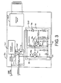
- Fig. 3 is an enlarged view of the inverter circuit.
- the power recovery circuit 12c3 includes a power supply voltage determining circuit 18, a backlight driving signal cutoff circuit 19, and a switchover circuit 20.
- the power supply voltage determining circuit 18 compares a power supply voltage from the main power supply circuit 12a with a specified voltage through a Zener diode 18a. If the power supply voltage is equal to or higher than the specified voltage, a determination current is output.
- the backlight driving signal cutoff circuit 19 outputs the power supply voltage from the main power supply circuit 12a to a base 20al of the second transistor 20a through a resistor A, so a backlight driving signal BL_on output from the microcomputer 11d2 is emitted to a ground terminal 21 from a collector 20a2 of the second transistor 20a through an emitter 20a3 to cut off the signal BL_on output to the protective circuit 17.
- the switchover circuit 20 outputs a determination current from the Zener diode 18a to the base 19a1 of the first transistor 19a.
- a current corresponding to the power supply voltage output from the main power supply circuit 12a is emitted from the collector 19a2 of the first transistor 19a to the ground terminal 21 through the emitter 19a3 to cut off the supply of the power supply voltage to the base 20a1 of the second transistor 20a through the resistor aA and supply the signal BL_on to the protective circuit 17.
- a breakdown current is allowed to flow in accordance with a voltage value of 20 volts or higher. If a voltage supplied from the main power supply circuit 12a is below 20 volts, it is determined that temporary blackout occurs. Further, the first transistor 19a and the second transistor 20a are npn type transistors. In this way, a voltage from the main power supply circuit 12a is lowered by use of the Zener diode and the npn type transistors, so a circuit can be configured by any commercially available inexpensive product. Further, if the Zener diode is used, a threshold value for determining that temporary blackout occurs can be readily changed by replacing the Zener diode.
- Fig. 4 shows functions of the power recovery circuit 12c3 under the condition that a voltage of 20 volts or higher is supplied from the main power supply circuit.
- Fig. 5 shows functions of the power recovery circuit 12c3 under the condition that a voltage of 20 volts or lower is supplied from the main power supply circuit.
- a voltage supplied from the main power supply circuit 12a is 20 volts or higher, the power supply voltage causes breakdown of the Zener diode 18a, and the Zener diode 18a outputs a breakdown current to the base 19a1 of the first transistor 19a.
- the power supply voltage is divided and output to the resistor A and then applied to the collector 19a2 of the first transistor 19a.
- a breakdown current flows through the base 19a1 of the first transistor 19a, so a current flowing through the collector 19a2 flows into the emitter 19a3 and is then output from the ground terminal 21.
- the signal BL_on flows through the base 17a1 of the transistor 17a of the protective circuit 17, so an actuating signal output from the inverter controlling IC12cl is sent to the switching circuit 12c2.
- the switching circuit 12c2 generates an output voltage for driving the backlight 13c.
- a voltage supplied from the main power supply circuit 12a is 20 volts or lower
- the power supply voltage of the main power supply circuit 12a is applied to the Zener diode 18a.
- the Zener diode 18a supplies no breakdown current.
- a current generated based on the divided power supply voltage at the resistor A does not flow through the first transistor 19a but through the base 20al of the second transistor 20a.
- the signal BL_on output from the microcomputer 11d2 is not output to the base 17al of the protective circuit 17 but to the ground terminal 21 of the second transistor 20a since the continuity between the collector 20a2 and the emitter 20a3 of the second transistor 20a is attained.
- an actuating signal of the inverter controlling IC12c1 is not output to the transistor 17a of the protective circuit 17 and the switching circuit 12c2 is not driven.
- Such reduction in voltage supplied from the main power supply circuit 12a is only temporary, and the supplied voltage returns to 20 volts or higher at once, with the result that the signal BL_on supplied from the microcomputer 11d2 is switched from OFF state to ON state, and the inverter controlling IC12c2 restarts controlling the driving of the switching circuit 12c2.
- the protective circuit 17 is integrated by use of the transistor 17a but may be integrated by use of a logic circuit in the inverter controlling IC12c1. If the protective circuit 17 is configured by the logic circuit in the inverter controlling IC12c1, the above functions can be realized by connecting an input terminal for the signal BL_on from the microcomputer 11d2 of the inverter controlling IC12c1 to the first transistor 19a of the backlight driving signal cutoff circuit 19 of the power recovery circuit 12c3.
- an inverter-circuit power supply circuit for supplying power to an inverter circuit supplied with a power supply voltage from a main power supply circuit through a main transformer and having a protective function of temporarily cutting off a backlight driving signal to thereby redrive the inverter circuit especially when the power supply voltage becomes lower than a specified voltage to stop the inverter circuit.
- the inverter-circuit power supply circuit cuts off the supply of backlight driving signals from the microcomputer by use of a power recovery circuit upon temporary blackout and redrives the inverter circuit without turning on the main power again.
Landscapes
- Engineering & Computer Science (AREA)
- Physics & Mathematics (AREA)
- Computer Hardware Design (AREA)
- General Physics & Mathematics (AREA)
- Theoretical Computer Science (AREA)
- Liquid Crystal (AREA)
- Liquid Crystal Display Device Control (AREA)
- Control Of Indicators Other Than Cathode Ray Tubes (AREA)
- Television Receiver Circuits (AREA)
- Circuit Arrangements For Discharge Lamps (AREA)
- Transforming Electric Information Into Light Information (AREA)
Abstract
Description
- The present invention relates to a backlight power supplying circuit for supplying power to a backlight. In particular, the invention relates to a backlight power supplying circuit having a function of protecting the circuit against voltage drop, and to a liquid crystal television (TV) with use of the backlight power supplying circuit.
- Fig. 6 shows a conventional backlight power supplying circuit. As shown in Fig. 6, a backlight power supplying circuit 1 includes a main
power supply circuit 3, amain transformer 4, aninverter circuit 5, atransformer 6, acontrol unit 8, and a determiningcircuit 9. The mainpower supply circuit 3 rectifies and reduces a voltage of a commercially available 100V AC power supply, which is input from aplug socket 2, and the voltage is divided at themain transformer 4 to thereby supply power to theinverter circuit 5. Further, themain transformer 4 supplies power to various circuits other than theinverter circuit 5. Theinverter circuit 5 is intended to increase the voltage divided through themain transformer 4 due to the switching action of a MOSFET etc. up to an output voltage level necessary for the backlight 7. In this case, such MOSFETs execute a switching function behind the control of theinverter controlling IC 5a incorporated into theinverter circuit 5.
Thecontrol unit 8 controls driving of the mainpower supply circuit 3 and theinverter circuit 5. In response to an instruction to turn the power on the backlight 7 by means of a remote controller (not shown), thecontrol unit 8 starts driving the mainpower supply circuit 3 and sends a signal BL_on that triggers theinverter controlling IC 5a to execute the switching function. As a result, theinverter circuit 5 boosts the power supply voltage input through themain transformer 4 and outputs the boosted voltage to the backlight 7 through thetransformer 6. Further, a secondary coil of thetransformer 6 makes determination about the output voltage for the backlight by means of the determiningcircuit 9. If the determiningcircuit 9 detects any abnormality in output voltage, a feedback signal is sent to thecontrol unit 8. Thecontrol unit 8 receives the feedback signal to control the power supply of the mainpower supply circuit 3. - However, if a voltage of the commercially available power supply, which is supplied from the
plug socket 2, drops due to temporary blackout (momentary blackout), a power supply voltage input from the mainpower supply circuit 3 through thetransformer 4 is, of course, lowered, with the result that a voltage level of the signal BL_on lowers. At this time, the inverter controlling IC 5a stops driving theinverter circuit 5 without recognizing the signal BL_on. The inverter controlling IC includes, as a protective functional unit, a protective circuit 5al that stops driving theinverter circuit 5 when a voltage level of the signal BL_on is lowered. Since the output voltage generated with theinverter circuit 5 is abnormally as high as 1000 V, the protective circuit temporarily cuts off the supply of the signal BL_on from the control unit 8 (cuts off a main power supply) to thereby prevent the backlight 7 from being damaged due to malfunction of theinverter circuit 5. Hence, upon such temporary blackout, a user needs to turn on the main power supply again to redrive the liquid crystal TV -
Japanese Unexamined Patent Application Publication No. 2004-355865 - The technique as disclosed in
Japanese Unexamined Patent Application Publication No. 2004-355865 - The present invention aims at providing a liquid crystal TV with use of an inverter-circuit power supply circuit for supplying power to an inverter circuit supplied with a power supply voltage from a main power supply circuit through a main transformer and having a protective function of temporarily cutting off a backlight driving signal to thereby redrive the inverter circuit especially when the power supply voltage becomes lower than a specified voltage to stop the inverter circuit. The inverter-circuit power supply circuit can redrive the inverter circuit without turning on a main power again upon temporary blackout.
- According to an aspect of the present invention, a liquid crystal television, comprising:
- a backlight for illuminating a liquid crystal panel to display an image;
- a main power supply circuit for rectifying an AC power into a DC power supply voltage;
- an inverter circuit for boosting the power supply voltage supplied from the main power supply circuit through a transformer and supplying power to the backlight;
- an inverter controlling integrated circuit (IC) for controlling a voltage boosted by the inverter circuit based on a backlight driving signal and causing, if the power supply voltage from the main power supply circuit is lower than a specified voltage, the inverter circuit to stop boosting a voltage;
- a protective circuit having a protective function of temporarily cutting off the backlight driving signal to redrive the inverter circuit when the power supply voltage becomes lower than the specified voltage to stop driving the inverter circuit; and
- a microcomputer for outputting the backlight driving signal to the inverter controlling IC,
- the inverter circuit including a power recovery circuit for temporarily cutting off the backlight driving signal output from the microcomputer when the power supply voltage of the main power supply circuit drops due to temporary blackout, based on a value of the power supply voltage from the main power supply circuit, and restarting supply of the backlight driving signal to the protective circuit when the value of the power supply voltage is increased up to the specified voltage or higher,
- the power recovery circuit including:
- a power supply voltage determining circuit for comparing the power supply voltage from the main power supply circuit with the specified voltage by use of a Zener diode, and outputting a determination current if the power supply voltage is equal to or higher than the specified voltage;
- a backlight driving signal cutoff circuit for outputting, if the determination current is not output, the power supply voltage from the main power supply circuit to a base of a second transistor by use of a resistor, and emitting the backlight driving signal from the microcomputer to a ground terminal connected to an emitter of the second transistor to cut off the backlight driving signal; and
- a switchover circuit for emitting, if the determination current is output to a base of a first transistor, a current based on the power supply voltage from the main power supply circuit to a ground terminal connected to an emitter of the first transistor to cut off supply of the power supply voltage to the base of the second transistor through the resistor to restart supply of the backlight driving signal to the protective circuit.
- According to this configuration, the inverter circuit applies an output voltage to the backlight based on DC power supplied from the main power supply circuit, and the protective circuit of the inverter controlling IC has a protective function of stopping boosting if the power supply voltage from the main power supply circuit is lower than a specified value due to temporary blackout. The protective function of the protective circuit can be cancelled by temporarily cutting off the backlight driving signal. The inverter circuit includes the power recovery circuit to cancel the protective function of the protective circuit upon temporary blackout. If the power supply voltage from the main power supply circuit lowers due to temporary blackout, the power recovery circuit temporarily cuts off the backlight driving signal from the microcomputer and restarts the supply of the signal to the protective circuit when the power supply voltage is increased up to the specified voltage or higher. To that end, the power recovery circuit includes the power supply voltage determining circuit, the backlight driving signal cutoff circuit, and the switchover circuit, and executes ON/OFF control over a backlight driving voltage from the microcomputer based on the power supply voltage from the main power supply circuit.
- According to another aspect of the invention, a backlight power supplying circuit includes:
- an inverter circuit for boosting a power supply voltage supplied from a main power supply circuit and supplying power to a backlight;
- an inverter controlling integrated circuit (IC) for controlling a voltage boosted by the inverter circuit based on a backlight driving signal and causing, if the power supply voltage from the main power supply circuit is lower than a specified voltage, the inverter circuit to stop boosting a voltage;
- a protective circuit for having a protective function of temporarily cutting off the backlight driving signal to redrive the inverter circuit when the power supply voltage becomes lower than the specified voltage to stop driving the inverter circuit; and
- a control unit for outputting the backlight driving signal to the inverter controlling IC,
- the inverter circuit for including a power recovery circuit for temporarily cutting off the backlight driving signal output from the microcomputer when the power supply voltage of the main power supply circuit drops due to temporary blackout, based on a value of the power supply voltage from the main power supply circuit, and restarting supply of the backlight driving signal to the protective circuit when the value of the power supply voltage is increased up to the specified voltage or higher,
- the power recovery circuit including:
- a power supply voltage determining circuit for comparing the power supply voltage from the main power supply circuit with the specified voltage by use of a Zener diode, and outputting a determination current if the power supply voltage is equal to or higher than the specified voltage;
- a backlight driving signal cutoff circuit for turning off the backlight driving signal to the protective circuit by emitting to a ground the backlight driving signal outputted from the control unit when the determination current is not inputted,
- a switchover circuitry for turning on the backlight driving signal outputted to the backlight driving signal the protective circuit by intercepting that the supply voltage is outputted to the backlight driving signal cutoff circuit if the determination current is inputted.
- According to this configuration, the inverter circuit applies an output voltage to the backlight based on DC power supplied from the main power supply circuit, and the protective circuit of the inverter controlling IC has a protective function of stopping boosting if the power supply voltage from the main power supply circuit is lower than a specified value due to temporary blackout. The protective function of the protective circuit can be cancelled by temporarily cutting off the backlight driving signal. The inverter circuit includes the power recovery circuit to cancel the protective function of the protective circuit upon temporary blackout. If the power supply voltage from the main power supply circuit lowers due to temporary blackout, the power recovery circuit temporarily cuts off the backlight driving signal from the microcomputer and restarts the supply of the signal to the protective circuit when the power supply voltage is increased up to the specified voltage or higher. To that end, the power recovery circuit includes the power supply voltage determining circuit, the backlight driving signal cutoff circuit, and the switchover circuit, and executes ON/OFF control over a backlight driving voltage from the microcomputer based on the power supply voltage from the main power supply circuit.
Hence, it is possible to accomplish an inverter-circuit power supply circuit for supplying power to an inverter circuit having a protective function of temporarily cutting off a backlight driving signal to thereby redrive the inverter circuit especially when the power supply voltage becomes lower than a specified voltage to stop the inverter circuit. The inverter-circuit power supply circuit can redrive the inverter circuit without turning on a main power again upon temporary blackout. - In the backlight power supplying circuit according to the present invention, the power supply voltage determining circuit determines whether or not the power supply voltage is not lower than a specified voltage by use of a Zener diode,
When the determination current is outputted, the backlight driving signal cutoff circuit outputs the supply voltage outputted from the main power circuit to the base of a transistor, the backlight driving signal outputted from the control unit is emitted to a ground through an emitter from the collector of the transistor, and
when the determination current is outputted, the switchover circuit turns on the backlight driving signal which is intercepting the supply voltage being outputted to the base of the transistor, and is outputted to the protection circuit. - According to this configuration, the power supply voltage determining circuit compares the power supply voltage with the specified voltage by use of a Zener diode. Further, the backlight driving signal cutoff circuit switchingly connects/disconnects between the collector and emitter of the second transistor based on the power supply voltage to thereby emit the backlight driving signal from the control unit to the ground terminal. The switchover circuit outputs a determination current from the power supply voltage determining circuit to the base of the first transistor to thereby control the second transistor to emit the backlight driving signal to the ground terminal.
Hence, the power recovery circuit can be configured by any available Zener diode or transistor, so the circuit configuration costs low In addition, the specified voltage can be changed by replacing the Zener diode, and conditions of the power recovery circuit can be easily changed. - Further, in the backlight power supplying circuit according to the present invention, the protective circuit is realized based on control logic of the inverter controlling IC.
- According to this configuration, the protective circuit may be realized based on control logic of the inverter controlling IC.
Hence, the present invention is applicable to an inverter controlling IC incorporating a protective circuit. -
- Fig. 1 is a block diagram of a liquid crystal TV;
- Fig. 2 is a block diagram of an analog substrate;
- Fig. 3 is an enlarged view of an inverter circuit;
- Fig. 4 shows how a current flows when a power supply voltage is 20 volts or higher;
- Fig. 5 shows how a power supply voltage of 20 volts or lower is applied; and
- Fig. 6 shows a conventional backlight power supplying circuit.
- A backlight power supplying circuit according to the present invention will be described in detail below based on a liquid crystal TV including the backlight power supplying circuit.
Hereinafter, embodiments of the present invention will be described in the following order. - (1) Configuration of Liquid Crystal TV
- (2) Configuration of Backlight power supplying circuit
- (3) Modified Example 1
- (4) Conclusion
- Referring to Figs. 1 to 5, a
liquid crystal TV 10 with use of the backlight power supplying circuit according to the present invention is described below. Fig. 1 is a block diagram of theliquid crystal TV 10 of this device. As shown in Fig. 1, theliquid crystal TV 10 includes adisplay device 15 including adigital substrate 11, ananalog substrate 12, aliquid crystal display 13, and aspeaker 14, and aremote controller 16. Functions of each part are described next. - On the
digital substrate 11, atuner unit 11a, avideo circuit 11b, avoice circuit 11c, and acontrol unit 11d are formed. As shown in Fig. 1, the components of thedigital substrate 11 are connected to thecontrol unit 11d through abus 11e, and execute their functions under the control of thecontrol unit 11d. Thecontrol unit 11d includes a microcomputer 11d2 as a control center, a recording unit 11d3 such as a ROM or RAM, and an infrared receiving/converting unit 11d1 receiving an actuating signal from theremote controller 16. If an operation key 16c of theremote controller 16 is pressed, aninfrared transmitter unit 16a transmits an infrared signal to an infrared receiving/converting unit 11d1, and then the infrared receiving/converting unit 11d1 converts the received infrared signal into an actuating signal of a predetermined voltage level to output the signal to the microcomputer 11d2. In response to the actuating signal from the infrared receiving/converting unit 11d1, the microcomputer 11d2 outputs control signals to each component on thedigital substrate 11 through thebus 11e based on control programs recorded on the recording unit 11d3. - Receiving the actuating signal from the
control unit 11d, thetuner unit 11a selects only a specific frequency band of airwaves received by an antenna 11a1 to adjust chroma based on the airwaves of the selected specific frequency band to generate a video signal and a voice signal. The generated video signal is sent to thevideo circuit 11b, and the voice signal is sent to thevoice circuit 11c. Thetuner unit 11a of this device may receive analog broadcasting based on a PLL method, both analog broadcasting and digital broadcasting, or only digital broadcasting. - The
video circuit 11b receives the generated video signal to generate RGB signals corresponding to RGB gray scales for displaying a screen and perform predetermined signal processing on the generated RGB signals. Further, thevideo circuit 11b decomposes the RGB signals in accordance with the number of pixels of aliquid crystal panel 13b as described later and then outputs the signals to theliquid crystal panel 13b. - The
voice circuit 11c receives the generated voice signal and performs signal processing such as amplification on the voice signal based on a control signal from thecontrol unit 11d. The voice signal subjected to the signal processing is sent to thespeaker 14 and output as voice afterward. - The
liquid crystal display 13 includes theliquid crystal panel 13b having pixels of liquid crystal material arranged in matrix, adriver circuit 13a for applying a driving voltage to theliquid crystal panel 13b, and abacklight 13c for illuminating theliquid crystal panel 13b from the back. Thedriver circuit 13a applies a driving voltage as an applied voltage to predetermined pixels of theliquid crystal panel 13b on the row basis, based on the RGB signals that are divided for each pixel of theliquid crystal panel 13b by thevideo circuit 11b. In theliquid crystal panel 13b, pixels of liquid crystal material are arranged in matrix; the orientation of crystal grains of the liquid crystal material is changed in accordance with the driving voltage. Such pixels include a set of three pixels corresponding to RGB. When thedriver circuit 13a applies a voltage, the transmittance of light from thebacklight 13c is changed in the specific pixels to thereby change RGB gray scales and display a color screen. - As described above, the
backlight 13c illuminates theliquid crystal panel 13b from the back. Thebacklight 13c serves as a light source for light transmitted through pixels. As a fluorescent tube used for thebacklight 13c, a cold-cathode tube can be used. Regarding a tube shape, the tube may be a U-shaped tube, a straight tube, or a pseudo U-shaped tube. - The
analog substrate 12 supplies power necessary for the abovedigital substrate 11 orliquid crystal display 13. To give a brief explanation of functions of theanalog substrate 12, thesubstrate 12 rectifies commercially available 100-volt power, followed by isolation with the transformer. Then, thesubstrate 12 outputs the power to each DC/DC converter side. On the DC/DC converter side, a voltage is boosted or reduced to thereby generate and supply a stabilized AC power to thedigital substrate 11 or theliquid crystal display 13. - Fig. 2 is a block diagram of the
analog substrate 12. As shown in Fig. 2, theanalog substrate 12 includes a mainpower supply circuit 12a, amain transformer 12b, aninverter circuit 12c, atransformer 12d, a detectingcircuit 12f, and afeedback control circuit 12e. Although not shown, there are provided plural DC/DC converters that generate a predetermined AC power based on the power supplied from the mainpower supply circuit 12a through themain transformer 12b, but the present invention relates to theinverter circuit 12c, so description about the converters is omitted here. A function of theanalog substrate 12 is described below. - The main
power supply circuit 12a converts the commercially available 100V AC power supplied from theplug socket 12g into a DC power after full-wave rectification, and then applies the DC power to the primary coil 12b1 of themain transformer 12b. A rectifying function of the mainpower supply circuit 12a of the present invention is realized by a bridge circuit including a diode or the like. A secondary coil 12b2 having a winding ratio different from that of the primary coil 12b1 is provided on the opposite side of the primary coil 12b1 of themain transformer 12b, and an electromotive force is generated on the secondary coil 12b2 due to mutual induction. Further, the electromotive force generated on the secondary coil 12b2 is applied to theinverter circuit 12c or each DC/DC converter (not shown) through voltage division. - The
inverter circuit 12c boosts a voltage with the switching circuit 12c2 based on the voltage applied by the secondary coil 12b2. The switching circuit 12c2 is composed of four MOSFETs, and the inverter controlling IC12cl controls the four MOSFETs to thereby generate an AC power having positive half cycle and negative half cycle of sine waves based on the DC power. Further, theinverter circuit 12c incorporates theprotective circuit 17 and a power recovery circuit 12c3 as described below. Provided that the power supply voltage of the secondary coil 12b2 is lower than the specified voltage, and theinverter circuit 12c is stopped, theprotective circuit 17 has a protective function of temporarily cutting off the supply of the backlight driving signal from the microcomputer 11d2 to redrive the inverter circuit. - The switching circuit 12c2 is driven by applying a divided one of the voltage value of the secondary coil 12b2 to the inverter controlling IC12cl and applying a signal BL_on as a backlight driving signal output from the microcomputer 11d2 of the
digital substrate 11 to theprotective circuit 17. In the embodiment of the present invention, a voltage of 24 volts generated with themain transformer 12b is divided, and the divided voltage of 5 volts is applied to the inverter controlling IC12c2. - The AC power generated with the switching circuit 12c2 is applied to the primary coil 12d1 of the
transformer 12d. A secondary coil 12d2 having a winding ratio different from that of the primary coil 12d1 is provided on the opposite side of the primary coil 12d1, and an electromotive force is also applied to the secondary coil 12d2 due to mutual induction to thereby supply power to thebacklight 13c. Further, the detectingcircuit 12f is connected to the secondary coil 12d2 of thebacklight 13c. The detectingcircuit 12f determines a voltage value output to thebacklight 13c. If the output voltage value is larger than a reference value, a feedback signal is output to thefeedback control circuit 12e. Thefeedback control circuit 12e receives the feedback signal and executes feedback control to adjust a voltage value output from the mainpower supply circuit 12a to the primary coil 12b1. - Fig. 3 is an enlarged view of the inverter circuit. As shown in Fig. 3, the power recovery circuit 12c3 includes a power supply
voltage determining circuit 18, a backlight drivingsignal cutoff circuit 19, and aswitchover circuit 20. The power supplyvoltage determining circuit 18 compares a power supply voltage from the mainpower supply circuit 12a with a specified voltage through aZener diode 18a. If the power supply voltage is equal to or higher than the specified voltage, a determination current is output. The backlight drivingsignal cutoff circuit 19 outputs the power supply voltage from the mainpower supply circuit 12a to a base 20al of thesecond transistor 20a through a resistor A, so a backlight driving signal BL_on output from the microcomputer 11d2 is emitted to aground terminal 21 from a collector 20a2 of thesecond transistor 20a through an emitter 20a3 to cut off the signal BL_on output to theprotective circuit 17. Theswitchover circuit 20 outputs a determination current from theZener diode 18a to the base 19a1 of thefirst transistor 19a. In this way, a current corresponding to the power supply voltage output from the mainpower supply circuit 12a is emitted from the collector 19a2 of thefirst transistor 19a to theground terminal 21 through the emitter 19a3 to cut off the supply of the power supply voltage to the base 20a1 of thesecond transistor 20a through the resistor aA and supply the signal BL_on to theprotective circuit 17. - Regarding the specifications of the
Zener diode 18a, a breakdown current is allowed to flow in accordance with a voltage value of 20 volts or higher. If a voltage supplied from the mainpower supply circuit 12a is below 20 volts, it is determined that temporary blackout occurs. Further, thefirst transistor 19a and thesecond transistor 20a are npn type transistors. In this way, a voltage from the mainpower supply circuit 12a is lowered by use of the Zener diode and the npn type transistors, so a circuit can be configured by any commercially available inexpensive product. Further, if the Zener diode is used, a threshold value for determining that temporary blackout occurs can be readily changed by replacing the Zener diode. - Functions of the power recovery circuit 12c3 are specifically described below.
Fig. 4 shows functions of the power recovery circuit 12c3 under the condition that a voltage of 20 volts or higher is supplied from the main power supply circuit. Fig. 5 shows functions of the power recovery circuit 12c3 under the condition that a voltage of 20 volts or lower is supplied from the main power supply circuit. As shown in Fig. 4, if a voltage supplied from the mainpower supply circuit 12a is 20 volts or higher, the power supply voltage causes breakdown of theZener diode 18a, and theZener diode 18a outputs a breakdown current to the base 19a1 of thefirst transistor 19a. Further, the power supply voltage is divided and output to the resistor A and then applied to the collector 19a2 of thefirst transistor 19a. At this time, a breakdown current flows through the base 19a1 of thefirst transistor 19a, so a current flowing through the collector 19a2 flows into the emitter 19a3 and is then output from theground terminal 21. At this time, the signal BL_on flows through the base 17a1 of thetransistor 17a of theprotective circuit 17, so an actuating signal output from the inverter controlling IC12cl is sent to the switching circuit 12c2. As a result, the switching circuit 12c2 generates an output voltage for driving thebacklight 13c. - Referring next to Fig. 5, if a voltage supplied from the main
power supply circuit 12a is 20 volts or lower, the power supply voltage of the mainpower supply circuit 12a is applied to theZener diode 18a. However, since the power supply voltage is 20 volts or lower, theZener diode 18a supplies no breakdown current. Hence, a current generated based on the divided power supply voltage at the resistor A does not flow through thefirst transistor 19a but through the base 20al of thesecond transistor 20a. Further, the signal BL_on output from the microcomputer 11d2 is not output to the base 17al of theprotective circuit 17 but to theground terminal 21 of thesecond transistor 20a since the continuity between the collector 20a2 and the emitter 20a3 of thesecond transistor 20a is attained. Hence, an actuating signal of the inverter controlling IC12c1 is not output to thetransistor 17a of theprotective circuit 17 and the switching circuit 12c2 is not driven. Such reduction in voltage supplied from the mainpower supply circuit 12a is only temporary, and the supplied voltage returns to 20 volts or higher at once, with the result that the signal BL_on supplied from the microcomputer 11d2 is switched from OFF state to ON state, and the inverter controlling IC12c2 restarts controlling the driving of the switching circuit 12c2. - In the
above inverter circuit 12c, theprotective circuit 17 is integrated by use of thetransistor 17a but may be integrated by use of a logic circuit in the inverter controlling IC12c1. If theprotective circuit 17 is configured by the logic circuit in the inverter controlling IC12c1, the above functions can be realized by connecting an input terminal for the signal BL_on from the microcomputer 11d2 of the inverter controlling IC12c1 to thefirst transistor 19a of the backlight drivingsignal cutoff circuit 19 of the power recovery circuit 12c3. - As set forth above, it is possible to provide a liquid crystal TV with use of an inverter-circuit power supply circuit for supplying power to an inverter circuit supplied with a power supply voltage from a main power supply circuit through a main transformer and having a protective function of temporarily cutting off a backlight driving signal to thereby redrive the inverter circuit especially when the power supply voltage becomes lower than a specified voltage to stop the inverter circuit. The inverter-circuit power supply circuit cuts off the supply of backlight driving signals from the microcomputer by use of a power recovery circuit upon temporary blackout and redrives the inverter circuit without turning on the main power again.
- Incidentally, it is needless to say that the present invention is not limited to the above embodiments. Those skilled in the art will readily recognize that the following alternative embodiments are within the scope of the present invention:
- interchangeable members and components described in the above embodiment can be used in various combinations as appropriate;
- although not described in the above embodiment, the members and components of the above embodiment can be replaced by any known members and components as appropriate in various combinations; and
- although not described in the above embodiment, the members and components of the above embodiment can be replaced by any conceivable alternative members and components based on the related art as appropriate in various combinations.
Claims (4)
- A liquid crystal television, comprising:a backlight for illuminating a liquid crystal panel to display an image;a main power supply circuit for rectifying an AC power into a DC power supply voltage;an inverter circuit for boosting the power supply voltage supplied from the main power supply circuit through a transformer and supplying power to the backlight;an inverter controlling integrated circuit (IC) for controlling a voltage boosted by the inverter circuit based on a backlight driving signal and causing, if the power supply voltage from the main power supply circuit is lower than a specified voltage, the inverter circuit to stop boosting a voltage;a protective circuit having a protective function of temporarily cutting off the backlight driving signal to redrive the inverter circuit when the power supply voltage becomes lower than the specified voltage to stop driving the inverter circuit; anda microcomputer for outputting the backlight driving signal to the inverter controlling IC,the inverter circuit including a power recovery circuit for temporarily cutting off the backlight driving signal output from the microcomputer when the power supply voltage of the main power supply circuit drops due to temporary blackout, based on a value of the power supply voltage from the main power supply circuit, and restarting supply of the backlight driving signal to the protective circuit when the value of the power supply voltage is increased up to the specified voltage or higher,the power recovery circuit including:a power supply voltage determining circuit for comparing the power supply voltage from the main power supply circuit with the specified voltage by use of a Zener diode, and outputting a determination current if the power supply voltage is equal to or higher than the specified voltage;a backlight driving signal cutoff circuit for outputting, if the determination current is not output, the power supply voltage from the main power supply circuit to a base of a second transistor by use of a resistor, and emitting the backlight driving signal from the microcomputer to a ground terminal connected to an emitter of the second transistor to cut off the backlight driving signal; anda switchover circuit for emitting, if the determination current is output to a base of a first transistor, a current based on the power supply voltage from the main power supply circuit to a ground terminal connected to an emitter of the first transistor to cut off supply of the power supply voltage to the base of the second transistor through the resistor to restart supply of the backlight driving signal to the protective circuit.
- A backlight power supplying circuit, comprising:an inverter circuit for boosting a power supply voltage supplied from a main power supply circuit and supplying power to a backlight;an inverter controlling integrated circuit (IC) for controlling a voltage boosted by the inverter circuit based on a backlight driving signal and causing, if the power supply voltage from the main power supply circuit is lower than a specified voltage, the inverter circuit to stop boosting a voltage;a protective circuit for having a protective function of temporarily cutting off the backlight driving signal to redrive the inverter circuit when the power supply voltage becomes lower than the specified voltage to stop driving the inverter circuit; anda control unit for outputting the backlight driving signal to the inverter controlling IC,the inverter circuit for including a power recovery circuit for temporarily cutting off the backlight driving signal output from the microcomputer when the power supply voltage of the main power supply circuit drops due to temporary blackout, based on a value of the power supply voltage from the main power supply circuit, and restarting supply of the backlight driving signal to the protective circuit when the value of the power supply voltage is increased up to the specified voltage or higher,the power recovery circuit including:a power supply voltage determining circuit for comparing the power supply voltage from the main power supply circuit with the specified voltage by use of a Zener diode, and outputting a determination current if the power supply voltage is equal to or higher than the specified voltage;a backlight driving signal cutoff circuit for turning off the backlight driving signal to the protective circuit by emitting to a ground the backlight driving signal outputted from the control unit when the determination current is not inputted,a switchover circuitry for turning on the backlight driving signal outputted to the backlight driving signal the protective circuit by intercepting that the supply voltage is outputted to the backlight driving signal cutoff circuit if the determination current is inputted.
- The backlight power supplying circuit according to claim 2, wherein the power supply voltage determining circuit determines whether or not the power supply voltage is not lower than a specified voltage by use of a Zener diode,
When the determination current is outputted, the backlight driving signal cutoff circuit outputs the supply voltage outputted from the main power circuit to the base of a transistor, the backlight driving signal outputted from the control unit is emitted to a ground through an emitter from the collector of the transistor, and
when the determination current is outputted, the switchover circuit turns on the backlight driving signal which is intercepting the supply voltage being outputted to the base of the transistor, and is outputted to the protection circuit. - The backlight power supplying circuit according to claim 2, wherein the protective circuit is realized based on control logic of the inverter controlling IC.
Applications Claiming Priority (1)
| Application Number | Priority Date | Filing Date | Title |
|---|---|---|---|
| JP2006110109A JP4164697B2 (en) | 2006-04-12 | 2006-04-12 | LCD television and backlight power supply circuit |
Publications (2)
| Publication Number | Publication Date |
|---|---|
| EP1845757A2 true EP1845757A2 (en) | 2007-10-17 |
| EP1845757A3 EP1845757A3 (en) | 2011-03-23 |
Family
ID=38255110
Family Applications (1)
| Application Number | Title | Priority Date | Filing Date |
|---|---|---|---|
| EP07007439A Withdrawn EP1845757A3 (en) | 2006-04-12 | 2007-04-11 | Liquid crystal television and backlight power supplying circuit |
Country Status (3)
| Country | Link |
|---|---|
| US (1) | US7525780B2 (en) |
| EP (1) | EP1845757A3 (en) |
| JP (1) | JP4164697B2 (en) |
Cited By (1)
| Publication number | Priority date | Publication date | Assignee | Title |
|---|---|---|---|---|
| CN108364613A (en) * | 2018-02-07 | 2018-08-03 | 青岛海信电器股份有限公司 | LED backlight drive circuit, LED backlight, television terminal |
Families Citing this family (7)
| Publication number | Priority date | Publication date | Assignee | Title |
|---|---|---|---|---|
| JP3123106U (en) * | 2006-04-19 | 2006-07-06 | 船井電機株式会社 | Voltage rise suppression circuit and panel type television apparatus |
| KR100714633B1 (en) * | 2006-06-20 | 2007-05-07 | 삼성전기주식회사 | LC backlight inverter |
| KR101461115B1 (en) * | 2007-10-31 | 2014-11-13 | 삼성디스플레이 주식회사 | Backlight device and liquid crystal display device having the same |
| KR101481701B1 (en) | 2008-08-22 | 2015-01-12 | 삼성디스플레이 주식회사 | Timing control apparatus and display device having the same |
| JP6529301B2 (en) * | 2015-03-24 | 2019-06-12 | 株式会社コロナ | Cable abnormality determination device, remote control, cable abnormality determination method, cable abnormality determination program, and water heater with remote control |
| KR102389836B1 (en) * | 2015-06-05 | 2022-04-25 | 삼성전자주식회사 | Power supply device, display apparatus having the same and method for power supply |
| KR102783871B1 (en) * | 2020-07-23 | 2025-03-21 | 삼성전자주식회사 | Display apparatus, control method thereof and integrated circuit chip |
Citations (2)
| Publication number | Priority date | Publication date | Assignee | Title |
|---|---|---|---|---|
| JPH08255690A (en) | 1996-03-21 | 1996-10-01 | Koito Mfg Co Ltd | Discharge lamp lighting circuit |
| EP1524648A2 (en) | 2003-10-17 | 2005-04-20 | Samsung Electronics Co., Ltd. | Power supply system and liquid crystal display device having the same |
Family Cites Families (5)
| Publication number | Priority date | Publication date | Assignee | Title |
|---|---|---|---|---|
| US6504691B1 (en) * | 1999-07-13 | 2003-01-07 | Kabushiki Kaisha Sanyo Denki Seisa Kusho | Safety enhanced transformer circuit |
| FR2830379B1 (en) * | 2001-10-03 | 2004-08-06 | Agence Spatiale Europeenne | DEVICE FOR PROTECTING A VOLTAGE SOURCE AND A LOAD SUPPLIED BY THE VOLTAGE SOURCE |
| JP2004342321A (en) | 2003-05-12 | 2004-12-02 | Matsushita Electric Works Ltd | Discharge lamp lighting device |
| KR100509501B1 (en) * | 2003-05-26 | 2005-08-22 | 삼성전자주식회사 | Apparatus for driving inverter in LCD monitor |
| JP2004355865A (en) | 2003-05-28 | 2004-12-16 | Funai Electric Co Ltd | Discharge tube lighting device |
-
2006
- 2006-04-12 JP JP2006110109A patent/JP4164697B2/en not_active Expired - Fee Related
-
2007
- 2007-04-11 EP EP07007439A patent/EP1845757A3/en not_active Withdrawn
- 2007-04-11 US US11/786,333 patent/US7525780B2/en not_active Expired - Fee Related
Patent Citations (2)
| Publication number | Priority date | Publication date | Assignee | Title |
|---|---|---|---|---|
| JPH08255690A (en) | 1996-03-21 | 1996-10-01 | Koito Mfg Co Ltd | Discharge lamp lighting circuit |
| EP1524648A2 (en) | 2003-10-17 | 2005-04-20 | Samsung Electronics Co., Ltd. | Power supply system and liquid crystal display device having the same |
Cited By (2)
| Publication number | Priority date | Publication date | Assignee | Title |
|---|---|---|---|---|
| CN108364613A (en) * | 2018-02-07 | 2018-08-03 | 青岛海信电器股份有限公司 | LED backlight drive circuit, LED backlight, television terminal |
| CN108364613B (en) * | 2018-02-07 | 2020-03-06 | 青岛海信电器股份有限公司 | LED backlight drive circuit, LED backlight lamp and television terminal |
Also Published As
| Publication number | Publication date |
|---|---|
| US20070241694A1 (en) | 2007-10-18 |
| US7525780B2 (en) | 2009-04-28 |
| EP1845757A3 (en) | 2011-03-23 |
| JP4164697B2 (en) | 2008-10-15 |
| JP2007287351A (en) | 2007-11-01 |
Similar Documents
| Publication | Publication Date | Title |
|---|---|---|
| US7525780B2 (en) | Liquid crystal television and backlight power supplying circuit | |
| US10332474B2 (en) | Display apparatus having power supply device with power factor compensation and power supply method thereof | |
| EP2590478A1 (en) | LED driving apparatus and method and display apparatus using the LED driving apparatus and method | |
| KR101925142B1 (en) | Power supply apparatus and display apparatus having the same | |
| US20140042819A1 (en) | Electronic apparatus and power management method | |
| US7531970B2 (en) | Power source driving circuits and controllers thereof | |
| US9985474B2 (en) | Display apparatus and power supplying method thereof | |
| KR20110044935A (en) | Display device and power supply method | |
| US8243008B2 (en) | Separately excited inverter circuit and liquid crystal display television | |
| GB2409357A (en) | Comparing output voltages of lamps | |
| US7902767B2 (en) | AC inverter capable of driving multiple lamps for LCD panel backlight | |
| EP1988753A2 (en) | Liquid crystal display apparatus and liquid crystal television | |
| US10176764B2 (en) | Power supply device, display apparatus having the same, and method for supplying power | |
| US20070052372A1 (en) | Display apparatus | |
| US7548229B2 (en) | Multi-display system and control method thereof | |
| US6327161B1 (en) | Power-saving circuit | |
| KR102663510B1 (en) | Electronic apparatus and the control method thereof | |
| KR20050037241A (en) | Power supply and liquid crystal display device having the same | |
| EP1988535B1 (en) | Display device and liquid crystal television | |
| US6989639B2 (en) | Television image receiving apparatus and CRT display apparatus | |
| KR101079363B1 (en) | Driver for plasma display panel having portection function | |
| US7936349B2 (en) | Power supply apparatus and flat-screen television set | |
| KR970008369B1 (en) | Overvoltage Protection and Indicators | |
| US8330877B2 (en) | Self-excited inverter and LCD television apparatus | |
| JP2005057379A (en) | Liquid crystal television receiver |
Legal Events
| Date | Code | Title | Description |
|---|---|---|---|
| PUAI | Public reference made under article 153(3) epc to a published international application that has entered the european phase |
Free format text: ORIGINAL CODE: 0009012 |
|
| AK | Designated contracting states |
Kind code of ref document: A2 Designated state(s): AT BE BG CH CY CZ DE DK EE ES FI FR GB GR HU IE IS IT LI LT LU LV MC MT NL PL PT RO SE SI SK TR |
|
| AX | Request for extension of the european patent |
Extension state: AL BA HR MK YU |
|
| PUAL | Search report despatched |
Free format text: ORIGINAL CODE: 0009013 |
|
| AK | Designated contracting states |
Kind code of ref document: A3 Designated state(s): AT BE BG CH CY CZ DE DK EE ES FI FR GB GR HU IE IS IT LI LT LU LV MC MT NL PL PT RO SE SI SK TR |
|
| AX | Request for extension of the european patent |
Extension state: AL BA HR MK RS |
|
| 17P | Request for examination filed |
Effective date: 20110824 |
|
| AKX | Designation fees paid |
Designated state(s): DE FR GB PL |
|
| 17Q | First examination report despatched |
Effective date: 20120227 |
|
| RIC1 | Information provided on ipc code assigned before grant |
Ipc: G09G 3/34 20060101AFI20140717BHEP Ipc: H05B 41/285 20060101ALI20140717BHEP |
|
| GRAP | Despatch of communication of intention to grant a patent |
Free format text: ORIGINAL CODE: EPIDOSNIGR1 |
|
| INTG | Intention to grant announced |
Effective date: 20141006 |
|
| STAA | Information on the status of an ep patent application or granted ep patent |
Free format text: STATUS: THE APPLICATION IS DEEMED TO BE WITHDRAWN |
|
| 18D | Application deemed to be withdrawn |
Effective date: 20150217 |