EP1843465A1 - Multiple feedback class-D amplifier - Google Patents
Multiple feedback class-D amplifier Download PDFInfo
- Publication number
- EP1843465A1 EP1843465A1 EP06425213A EP06425213A EP1843465A1 EP 1843465 A1 EP1843465 A1 EP 1843465A1 EP 06425213 A EP06425213 A EP 06425213A EP 06425213 A EP06425213 A EP 06425213A EP 1843465 A1 EP1843465 A1 EP 1843465A1
- Authority
- EP
- European Patent Office
- Prior art keywords
- feedback
- signal
- amplifier
- load
- loop
- Prior art date
- Legal status (The legal status is an assumption and is not a legal conclusion. Google has not performed a legal analysis and makes no representation as to the accuracy of the status listed.)
- Withdrawn
Links
- 230000000694 effects Effects 0.000 abstract description 4
- 238000010586 diagram Methods 0.000 description 18
- 238000001914 filtration Methods 0.000 description 3
- 230000010355 oscillation Effects 0.000 description 3
- XUIMIQQOPSSXEZ-UHFFFAOYSA-N Silicon Chemical compound [Si] XUIMIQQOPSSXEZ-UHFFFAOYSA-N 0.000 description 2
- 230000003467 diminishing effect Effects 0.000 description 2
- 238000000034 method Methods 0.000 description 2
- 229910052710 silicon Inorganic materials 0.000 description 2
- 239000010703 silicon Substances 0.000 description 2
- 230000003595 spectral effect Effects 0.000 description 2
- 230000002238 attenuated effect Effects 0.000 description 1
- 239000003990 capacitor Substances 0.000 description 1
- 238000004519 manufacturing process Methods 0.000 description 1
- 239000000463 material Substances 0.000 description 1
- 238000013178 mathematical model Methods 0.000 description 1
- 238000005457 optimization Methods 0.000 description 1
- 230000010363 phase shift Effects 0.000 description 1
- 230000035945 sensitivity Effects 0.000 description 1
- 238000004088 simulation Methods 0.000 description 1
- 230000005236 sound signal Effects 0.000 description 1
- 238000011144 upstream manufacturing Methods 0.000 description 1
- 238000004804 winding Methods 0.000 description 1
Images






Classifications
-
- H—ELECTRICITY
- H03—ELECTRONIC CIRCUITRY
- H03F—AMPLIFIERS
- H03F3/00—Amplifiers with only discharge tubes or only semiconductor devices as amplifying elements
- H03F3/20—Power amplifiers, e.g. Class B amplifiers, Class C amplifiers
- H03F3/21—Power amplifiers, e.g. Class B amplifiers, Class C amplifiers with semiconductor devices only
- H03F3/217—Class D power amplifiers; Switching amplifiers
- H03F3/2175—Class D power amplifiers; Switching amplifiers using analogue-digital or digital-analogue conversion
-
- H—ELECTRICITY
- H03—ELECTRONIC CIRCUITRY
- H03F—AMPLIFIERS
- H03F1/00—Details of amplifiers with only discharge tubes, only semiconductor devices or only unspecified devices as amplifying elements
- H03F1/32—Modifications of amplifiers to reduce non-linear distortion
-
- H—ELECTRICITY
- H03—ELECTRONIC CIRCUITRY
- H03F—AMPLIFIERS
- H03F1/00—Details of amplifiers with only discharge tubes, only semiconductor devices or only unspecified devices as amplifying elements
- H03F1/34—Negative-feedback-circuit arrangements with or without positive feedback
-
- H—ELECTRICITY
- H03—ELECTRONIC CIRCUITRY
- H03F—AMPLIFIERS
- H03F1/00—Details of amplifiers with only discharge tubes, only semiconductor devices or only unspecified devices as amplifying elements
- H03F1/42—Modifications of amplifiers to extend the bandwidth
- H03F1/48—Modifications of amplifiers to extend the bandwidth of aperiodic amplifiers
-
- H—ELECTRICITY
- H03—ELECTRONIC CIRCUITRY
- H03F—AMPLIFIERS
- H03F2200/00—Indexing scheme relating to amplifiers
- H03F2200/153—Feedback used to stabilise the amplifier
Definitions
- This invention relates to electronic amplifiers and more particularly to a feedback amplifier in which a class D amplifier and a low-pass filter connected in cascade thereto are fedback through two feedback loops of the voltage signal supplied to a load.
- D amplifiers are widely used because they are characterized by a relatively small power consumption and reduced size and weight.
- One of the drawbacks due to the use of a class D audio amplifier is the need of interposing between the power stage and the loudspeaker a filter for extracting the low-frequency spectral content (from about 20Hz to about 20kHz) from the output of the power stage.
- the functioning principle of a class D amplifier consists in modulating a carrier of a frequency ⁇ c with a signal to be amplified of frequency ⁇ s much smaller than ⁇ c , and in demodulating the output signal generated by the power stage.
- a possible modulation appropriate for this objective is the PWM modulation (Pulse Width Modulation), to which reference will be made hereinafter.
- the modulated signal is a square wave with a fixed frequency and duty-cycle adjusted in function of the signal to be amplified.
- the information content relative to the amplified signal may then be extracted from the PWM modulated signal by a low-pass LC passive filter (called also demodulation filter).
- a low-pass LC passive filter called also demodulation filter
- a snubber network S N is connected in parallel to the load such to reduce the load voltage ripple.
- the core of inductors for audio filtering applications is of a material having a non negligible hysteresis, therefore the value of the inductance L varies and depends on the current that flows through the winding. This phenomenon is even more evident when the core is relatively small (low cost).
- the filtering operation introduces a nonlinearity that directly influences the amplified signal.
- the THD (Total Harmonic Distortion) of a class D amplifier is strongly influenced by the performances of the demodulation filter, because the filter is one of the main sources of distortion in switching amplifiers.
- the LC filter is connected in series to the load and interferes with the direct control of the amplifier of the loudspeaker making the frequency response depend from the load, as shown in the Bode diagrams of Figure 2.
- the frequency response becomes even less regular when the loads, such as loudspeakers, are not purely resistive.
- a cut-off frequency ⁇ T of the cascade low-pass filter + load larger than 20kHz.
- the cut-off frequency ⁇ T is always chosen as a compromise between the need of dampening high frequency components of the output signals generated by the power stage and the requisite of the largest possible frequency response.
- the patent US 4,456,872 discloses a switching amplifier that has a voltage and a current feedback loop.
- COM Controlled Oscillation Modulator
- the presence of a feedback at the output of the power stage generates aliasing that, generally speaking penalizes the linearity performances of the system.
- the functioning is based on a self-oscillating circuit (the input signal modulates the duty-cycle of the square wave at the output of the oscillator) with a variable oscillation frequency. This characteristic may penalize the system from the point of view of the EMI (ElectroMagnetic Interference) and makes difficult the synchronization of other signals with the oscillation frequency of the circuit.
- EMI ElectroMagnetic Interference
- This invention provides a new feedback architecture for a PWM switching audio amplifier, capable of compensating the effects of the demodulation filter through at least two feedback paths of the voltage applied to a load without penalizing the overall loop gain of the device.
- Each of the feedback paths includes a respective network (or filter) for compensating a respective frequency pole of the cascade low-pass filter + load and establishing a certain band pass.
- these networks are passive networks.
- the feedback amplifier allows for a further reduction of the distortion because the fedback signal is that output by the low-pass demodulation filter, in cascade to the class D amplifier, differently from the prior art amplifiers that feedback a signal that occupies an unlimited band generated from the power stage (that is the class D amplifier), thus generating aliasing phenomena that degrade the linearity performances of the circuit.
- the proposed architecture allows, with the same pass band of known amplifiers, to reduce the high frequency voltage ripple on the supplied load significantly lowering electromagnetic emissions.
- the demodulation filter introduces a phase shift that may make the system unstable if a simple feedback is adopted.
- this problem is effectively eliminated by realizing at least two feedback paths with each loop comprising at least a filter for compensating the poles of the low-pass demodulation filter and fixing (generally, widening) the pass band of the amplifier.
- Figure 4 depicts a preferred architecture of a device of this invention, including:
- one of the poles of G loop,1 introduced by the LC low-pass filter is compensated by choosing the parameters that define the network R ⁇ 1 introduced in the feedback loop, the transfer function of G loop, 1 as depicted in Figure 5b and the transfer function of V out V x as shown in Figure 6 are obtained.
- Compensation of the pole at a cut-off frequency ⁇ T is achieved by positioning at the same frequency a zero of the network (filter) introduced in the feedback path.
- the overall gain and also the cut-off frequency ⁇ ex of the transfer function V out V i ⁇ n are determined and thus also the pass band of the feedback amplifier of this invention.
- Figure 8 depicts a prototype of an amplifier made according to this invention, in which two control loops of the load voltage Vout, the respective feedback paths of which include the networks R ⁇ 1 and R ⁇ 2 , both fundamental for the stability of the system, while Figure 9 depicts in a more detailed fashion the same circuit, with a current input ( I in ).
- the reference carrier I rif is a square wave at a fixed frequency ⁇ c , that may be fixed in a broad frequency range.
- the frequency ⁇ c should be chosen such to prevent possible interferences with devices operating in the same electromagnetic environment.
- the output of the power stage, immediately upstream the low-pass filter LC, is a PWM wave.
- Using a square wave as a reference carrier instead of a triangular wave, as typically done in PWM modulators at fixed frequency is advantageous because a square waveform may be more easily generated than a triangular waveform.
- the reference carrier is provided in the feedback loop and it is added to at least a feedback signal provided by a respective feedback loop, that reduces sensitivity of the device in respect to the characteristics of the square wave reference current, thus the architecture is further simplified.
- Figure 10 depicts the equivalent circuit of the linearized internal loop.
- a mathematical model involving the averages of the state variables (available in literature, for example in: R. D. Middlebrook - “Small-Signal Modelling of Pulse Width Modulation Switched-Mode Power Converters", Proceedings of the IEEE, Vol. 76, pp.343-354, No. 4, April 1988 ) is used, the square wave carrier being integrated and a corresponding triangular wave being on the node Y.
- the equivalent gain of the cascade DRIVERS + POWER STAGE of Figure 9 is indicated with D.
- the block with gain K 1 introduced in the feedback loop allows to attenuate the fedback signal and may even be a simple resistive voltage divider.
- the pair R 1 - C 1 introduces a zero at a frequency ⁇ T in the transfer function of the loop gain G loop,in of the inner loop, that compensates one of the poles introduced in the cascade of the low-pass filter + load (neglecting for sake of ease the effect of the snubber network, as shown in Figure 12a).
- This condition makes the Bode diagram of the module of the loop gain G loop,in cross the axis at 0dB with a slope not larger than - 40dB/dec. Tests demonstrated that, by choosing properly the various parameters, a phase margin sufficient to make stable the innermost loop can be obtained
- Figure 11 depicts the Bode diagram of the module of the loop gain G loop,in while the frequency diagram of the transfer function V out / V x is depicted in Figure 12b.
- Figure 13 schematically depicts the external loop of the system, with a loop gain G loop,ex .
- the blocks with gain K 2 and K 3 are attenuators, simply made of resistive voltage dividers.
- the resistor R 2 and the capacitor C 2 allow to compensate a pole of the transfer function of the loop gain G loop,ex of the outer loop by introducing a zero at a frequency ⁇ in , as shown by the Bode diagram of Figure 14. Even in this case, the Bode diagram of the module of the loop gain G loop,ex crosses the axis at 0dB with a slope not larger than -40dB/dec, thus it is possible to obtain a phase margin sufficient for making stable the outermost loop by properly designing the parameters of the circuit.
- K 3 and R define the gain of the circuit and contribute to determine the band (equal to ⁇ ex ) of the feedback amplifier of this invention.
- the block K 2 allows to shift up or down the characteristic of the module of the loop gain G loop,ex thus allowing an optimization of the phase margin.
- the gain K 2 by diminishing the gain K 2 , it is possible to maintain the same loop gain G loop,ex by diminishing the capacitance C 2 , thus reducing the silicon area occupation. This is highly desirable for integrating the device.
- the gain K 3 allows to limit the value of R, thus to reduce the relative silicon area occupation.
Landscapes
- Engineering & Computer Science (AREA)
- Power Engineering (AREA)
- Physics & Mathematics (AREA)
- Nonlinear Science (AREA)
- Amplifiers (AREA)
Abstract
Description
- This invention relates to electronic amplifiers and more particularly to a feedback amplifier in which a class D amplifier and a low-pass filter connected in cascade thereto are fedback through two feedback loops of the voltage signal supplied to a load.
- It is becoming even more difficult to realize high power linear amplifiers of relatively small size with an ever increasing number of channels to be amplified.
- The so-called D amplifiers are widely used because they are characterized by a relatively small power consumption and reduced size and weight. One of the drawbacks due to the use of a class D audio amplifier is the need of interposing between the power stage and the loudspeaker a filter for extracting the low-frequency spectral content (from about 20Hz to about 20kHz) from the output of the power stage.
- The functioning principle of a class D amplifier consists in modulating a carrier of a frequency ƒc with a signal to be amplified of frequency ƒs much smaller than ƒc, and in demodulating the output signal generated by the power stage. A possible modulation appropriate for this objective is the PWM modulation (Pulse Width Modulation), to which reference will be made hereinafter. In this case, the modulated signal is a square wave with a fixed frequency and duty-cycle adjusted in function of the signal to be amplified.
- As shown in Figure 1, the information content relative to the amplified signal may then be extracted from the PWM modulated signal by a low-pass LC passive filter (called also demodulation filter).
- Preferably, a snubber network SN is connected in parallel to the load such to reduce the load voltage ripple.
- The core of inductors for audio filtering applications is of a material having a non negligible hysteresis, therefore the value of the inductance L varies and depends on the current that flows through the winding. This phenomenon is even more evident when the core is relatively small (low cost).
- Therefore, the filtering operation introduces a nonlinearity that directly influences the amplified signal. As a consequence, the THD (Total Harmonic Distortion) of a class D amplifier is strongly influenced by the performances of the demodulation filter, because the filter is one of the main sources of distortion in switching amplifiers.
- Moreover, the LC filter is connected in series to the load and interferes with the direct control of the amplifier of the loudspeaker making the frequency response depend from the load, as shown in the Bode diagrams of Figure 2. The frequency response becomes even less regular when the loads, such as loudspeakers, are not purely resistive.
- In order to prevent a modulation of the frequency response in function of the load it is preferable to choose a cut-off frequency ƒT of the cascade low-pass filter + load larger than 20kHz. In general the cut-off frequency ƒT is always chosen as a compromise between the need of dampening high frequency components of the output signals generated by the power stage and the requisite of the largest possible frequency response.
- The possibility of introducing a filter inside a feedback loop would allow a reduction of the output harmonic distortion by compensating eventual nonlinearities introduced by the filter, or would allow a reduction of the costs of the reactive elements of the filter (a cost that in practice may be close to the cost of the whole amplifier), thus keeping unchanged the THD of the whole system. Moreover, by introducing a feedback of the output of the filter an enhanced control of the frequency response of the amplifier on the load could be expected, thus making it less sensible to load variations.
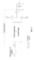
- However, feedbacking the system in a classic manner by using the output of the filter, as shown in Figure 3, would be a hardly affordable way because of the strong outphasing introduced by the LC pair that imposes a relevant reduction of the loop gain of the circuit in order to stabilize the system. As a consequence, this solution is not capable of reducing distortion nor of widening the frequency response.
- Several feedback amplifiers are described in literature.
- The patent
US 4,456,872 discloses a switching amplifier that has a voltage and a current feedback loop. - The presence of a feedback current complicates the circuit structure and requires a current sensor that increases relevantly fabrication costs of the system.
- The article "A Novel Audio Power Amplifier Topology with High Efficiency and State-of-the-Art Perform", by T. Frederiksen, H. Bengtsson and K. Nielsen, 109th AES Convention, 2000 September 22-25, Los Angeles, California, USA, discloses a switched power audio amplifier with at least two feedback paths, one of which is connected directly to the output of the power stage according to a COM (Controlled Oscillation Modulator) technique.
- The presence of a feedback at the output of the power stage generates aliasing that, generally speaking penalizes the linearity performances of the system. Moreover, the functioning is based on a self-oscillating circuit (the input signal modulates the duty-cycle of the square wave at the output of the oscillator) with a variable oscillation frequency. This characteristic may penalize the system from the point of view of the EMI (ElectroMagnetic Interference) and makes difficult the synchronization of other signals with the oscillation frequency of the circuit.
- The article "High Fidelity Pulse Width Modulation Amplifiers based on Novel Double Loop Feedback Techniques", by N. Anderskouv, K. Nielsen, M. A. E. Denmark, 100th AES Convention, 1996 May 11-14, Copenhagen, discloses a power audio amplifier with a voltage feedback loop and a current feedback loop.
- Besides the drawbacks due to the presence of the previously mentioned current feedback, the loop gain is unsatisfactory.
- The article "An Asynchronous switching high-end power amplifier", by P. van der Hulst, A. Veltman e R. Groeneberg, 112th AES Convention, 2002 May 10-13, Munich, Germany, discloses a switching power amplifier with current feedback that is affected by the above mentioned drawbacks due to the current feedback.
- A new architecture of a feedback amplifier easy to realize that solves the above mentioned problems of distortion and worsening of the frequency response, due to the presence of the demodulation low-pass filter has now been found.
- This invention provides a new feedback architecture for a PWM switching audio amplifier, capable of compensating the effects of the demodulation filter through at least two feedback paths of the voltage applied to a load without penalizing the overall loop gain of the device. Each of the feedback paths includes a respective network (or filter) for compensating a respective frequency pole of the cascade low-pass filter + load and establishing a certain band pass.
- According to an embodiment of this invention, these networks (or filters) are passive networks.
- The feedback amplifier allows for a further reduction of the distortion because the fedback signal is that output by the low-pass demodulation filter, in cascade to the class D amplifier, differently from the prior art amplifiers that feedback a signal that occupies an unlimited band generated from the power stage (that is the class D amplifier), thus generating aliasing phenomena that degrade the linearity performances of the circuit.
- Moreover, the proposed architecture allows, with the same pass band of known amplifiers, to reduce the high frequency voltage ripple on the supplied load significantly lowering electromagnetic emissions.
- The invention is defined in the annexed claims.
- The invention will be described referring to the attached drawings, wherein:
- Figure 1 illustrates schematically the functioning principle of a switching amplifier;
- Figure 2 shows the frequency response of the cascade low-pass filter + load + snubber network for different values of the purely resistive load Rload (with L=50 µH, C=1 µF);
- Figure 3 shows an example of a system fedback with a filter inside the feedback loop;
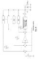
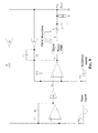
- Figure 4 is a block diagram of the proposed solution;
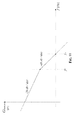
- Figure 5a and 5b are respectively the linearized circuit of the internal loop and the diagram of the module of the loop gain;
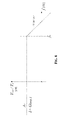
- Figure 6 is a Bode diagram of the transfer function Vout /Vx- ;
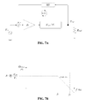
- Figures 7a and 7b are respectively a block diagram of the external loop and the relative Bode diagram of the loop gain;
- Figure 8 is a block diagram of an embodiment of this invention;
- Figure 9 is a block diagram of a second embodiment of this invention;
- Figure 10 is a detailed view of the internal loop of the circuit of Figure 9;
- Figure 11 is a Bode diagram of the module of the gain of the internal loop Gloop,in of the circuit of Figure 10;
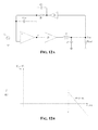
- Figure 12a is a detailed view of the internal loop of the circuit of Figure 9 with a generator of an input signal Vx ;
- Figure 12b shows the Bode diagram of the transfer function VoutVx- of the loop of Figure 12a;
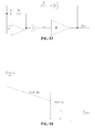
- Figure 13 shows schematically the outermost loop of the circuit of Figure 9;
- Figure 14 is a Bode diagram of the gain of the loop of Figure 13;
- Figure 15 shows a classic voltage switching amplifier with feedback of the output of the power stage;
- Figure 16 is a diagram of the frequency response of the device of this invention of Figure 9 for different values of the purely resistive load Rload (with L=50 µH,C=1 µF).
- Indeed, the demodulation filter introduces a phase shift that may make the system unstable if a simple feedback is adopted. According to this invention, this problem is effectively eliminated by realizing at least two feedback paths with each loop comprising at least a filter for compensating the poles of the low-pass demodulation filter and fixing (generally, widening) the pass band of the amplifier.
- Figure 4 depicts a preferred architecture of a device of this invention, including:
- a plurality of feedback paths of the load voltage downstream the reconstruction filter LC;
- a fixed frequency clock that defines the frequency of the output PWM waveform.
- The stability of the distinct feedback loops, from the innermost with a transfer function of the loop gain G loop,1, to the outermost with a transfer function Gloop,n , is analyzed herein below.
- For better understanding how the device of this invention works, that for simplicity of analysis is supposed linear, let us consider a circuit with only two loops. Moreover, let us assume that the feedback loop includes a passive network, described by the following transfer function:


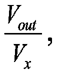
- Considering only the innermost loop, shown in Figure 5a, of the amplifier of this invention, one of the poles of Gloop,1 introduced by the LC low-pass filter is compensated by choosing the parameters that define the network Rƒ 1 introduced in the feedback loop, the transfer function of G loop,1 as depicted in Figure 5b and the transfer function of

- Compensation of the pole at a cut-off frequency ƒT is achieved by positioning at the same frequency a zero of the network (filter) introduced in the feedback path.
- By substituting the inner loop with a block with a transfer function


- By optionally adding two further outer feedback paths (that is paths around the previously illustrated two loops) of the load voltage Vout, it is possible to vary (typically to increase) the cut-off frequency of the system or the overall loop gain of the device. Increasing the overall loop gain is desirable because it determines a reduction of the distortion introduced by the system on the signal to be amplified.
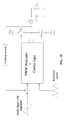
- Figure 8 depicts a prototype of an amplifier made according to this invention, in which two control loops of the load voltage Vout, the respective feedback paths of which include the networks Rƒ 1 and Rƒ 2, both fundamental for the stability of the system, while Figure 9 depicts in a more detailed fashion the same circuit, with a current input (Iin ).
- In general, the presence of only two feedback paths is sufficient for satisfactorily compensating the negative effects of the LC filter and obtaining a high loop gain.
- Preferably, the reference carrier Irif is a square wave at a fixed frequency ƒc, that may be fixed in a broad frequency range. The frequency ƒc should be chosen such to prevent possible interferences with devices operating in the same electromagnetic environment. The output of the power stage, immediately upstream the low-pass filter LC, is a PWM wave.
- Using a square wave as a reference carrier instead of a triangular wave, as typically done in PWM modulators at fixed frequency is advantageous because a square waveform may be more easily generated than a triangular waveform.
- According to a preferred embodiment of this invention, the reference carrier is provided in the feedback loop and it is added to at least a feedback signal provided by a respective feedback loop, that reduces sensitivity of the device in respect to the characteristics of the square wave reference current, thus the architecture is further simplified.
- For studying the stability of the system let us refer to Figure 10, that depicts the equivalent circuit of the linearized internal loop. For linearizing the loop, a mathematical model involving the averages of the state variables (available in literature, for example in: R. D. Middlebrook - "Small-Signal Modelling of Pulse Width Modulation Switched-Mode Power Converters", Proceedings of the IEEE, Vol. 76, pp.343-354, No. 4, April 1988) is used, the square wave carrier being integrated and a corresponding triangular wave being on the node Y. The equivalent gain of the cascade DRIVERS + POWER STAGE of Figure 9 is indicated with D.
- The block with gain K 1 introduced in the feedback loop allows to attenuate the fedback signal and may even be a simple resistive voltage divider. The pair R 1-C 1 introduces a zero at a frequency ƒT in the transfer function of the loop gain Gloop,in of the inner loop, that compensates one of the poles introduced in the cascade of the low-pass filter + load (neglecting for sake of ease the effect of the snubber network, as shown in Figure 12a). This condition makes the Bode diagram of the module of the loop gain Gloop,in cross the axis at 0dB with a slope not larger than - 40dB/dec. Tests demonstrated that, by choosing properly the various parameters, a phase margin sufficient to make stable the innermost loop can be obtained
- Figure 11 depicts the Bode diagram of the module of the loop gain Gloop,in while the frequency diagram of the transfer function Vout /Vx is depicted in Figure 12b.
- Figure 13 schematically depicts the external loop of the system, with a loop gain Gloop,ex. The inner loop has been substituted with a block with a transfer function H=Vout /Vx. Preferably, the blocks with gain K 2 and K 3 are attenuators, simply made of resistive voltage dividers.
- The resistor R 2 and the capacitor C 2 allow to compensate a pole of the transfer function of the loop gain Gloop,ex of the outer loop by introducing a zero at a frequency ƒin, as shown by the Bode diagram of Figure 14. Even in this case, the Bode diagram of the module of the loop gain Gloop,ex crosses the axis at 0dB with a slope not larger than -40dB/dec, thus it is possible to obtain a phase margin sufficient for making stable the outermost loop by properly designing the parameters of the circuit.
- The values of K 3 and R define the gain of the circuit and contribute to determine the band (equal to ƒex) of the feedback amplifier of this invention. The block K 2 allows to shift up or down the characteristic of the module of the loop gain Gloop,ex thus allowing an optimization of the phase margin.
- Moreover, by diminishing the gain K 2, it is possible to maintain the same loop gain Gloop,ex by diminishing the capacitance C 2, thus reducing the silicon area occupation. This is highly desirable for integrating the device. Similarly, the gain K 3 allows to limit the value of R, thus to reduce the relative silicon area occupation.
- Among the advantages that the amplifier of this invention offers compared to known amplifiers are:
- a) Compensation of nonlinearity introduced by the LC filter:
tests carried out on prototypes realized by the applicant confirm that the device of this invention sensibly reduces nonlinearity of the low-pass demodulation filter, even by two orders of magnitude with only two feedback loops. This allows to reduce the total harmonic distortion THD of the amplifier or alternatively for the same linearity performances, to use low cost reactive components. - b) Possibility of reducing the radiated emission:
from the previous considerations emerges that the band B of the amplifier may be made independent from the cut-off frequency ƒT of the cascade low-pass filter + load. It is possible to obtain B≈k20H z , even if ƒT <k 20H z, thus, in respect to a traditional circuit architecture (that is with a demodulating filter external to the feedback loop), the proposed architecture allows to attenuate more strongly the spectral components at high frequency of the amplified signal (that are inevitably present even after having filtered a PWM modulation signal).
Indeed, in the classical architecture of switching amplifier of Figure 15 with feedback at the output of the power stage, it is necessary to impose ƒT ≈ B for having a band-pass of B≈k20H z. By supposing that the frequency of the reference carrier is ƒc = 10B, the main harmonic frequency of the carrier is attenuated on the load by about 40dB in respect to the amplitude of the carrier output by the power stage.
By contrast, with the novel architecture of this invention it is possible to obtain B ≈k20H z even imposing
It should be noticed that the Power Bandwidth (PB) of the amplifier (that is the bandwidth inside which it is possible to have an amplified output signal with the largest amplitude allowed by the supply voltage of the power stage) is in both cases limited by the frequency ƒT. Therefore, by referring to the previous example, for the amplifier of this invention there is a PB of about
- c) Control of the frequency response:
the fact that the low-pass filter LC is inside the feedback loop ensures that the amplifier has a direct control of the amplified signal applied to the loudspeaker, without interposing elements connected in series or in parallel that may modify the frequency response. Figure 16 shows a sample frequency response on purely resistive loads, obtained with the amplifier of this invention depicted in Figure 9 by using the same filtering components used for the simulation of Figure 2.
By comparing the Bode's diagrams of Figure 16 and Figure 2 it is immediately recognized that the amplifier of this invention has a pass band much larger than that of the classic amplifier of Figure 1 and has a practically flat frequency response in the audible band because the frequency poles of the amplifier are positioned outside the audible band. The amplifier of this invention is characterized by a frequency response in the audible band that is substantially independent from the supplied load and it is the more regular the larger the overall loop gain in this frequency band is.
Claims (5)
- A signal amplifier, comprising:a class D amplifier generating a square wave voltage signal that is switched in function of an intermediate signal applied on an input thereof,a low-pass filter input with the square wave voltage signal generated by said class D amplifier for applying a filtered replica (Vout) of said signal to be amplified to a load (Rload),at least a feedback path of said filtered replica signal (Vout) applied to said load (Rload), generating a feedback signal,circuit means input at least with said feedback signal and said signal to be amplified, generating said an intermediate signal applied to said class D amplifier,characterized in that it comprises
a second feedback path of said filtered replica signal (Vout) supplied to the load (Rload), generating a second feedback signal input to said circuit means;
each of said feedback paths includes at least a filter for compensating a respective frequency pole of the transfer function of the cascade of the low-pass filter with the load (Rload) and for establishing at least a certain band pass of the device. - The feedback amplifier of claim 1, comprising at least a third feedback path of said filtered replica signal (Vout) supplied to the load, generating a third feedback signal input to said circuit means, comprising a filter for establishing at least a parameter of the transfer function of the device chosen in the group composed of the phase margin, the cut-off frequency, the total harmonic distortion, the loop gain and the gain of said device.
- The feedback amplifier of claim 1 or 2, wherein said circuit means generate the intermediate signal applied to said class D amplifier as a linear combination of said feedback signals, of the signal to be amplified and of an externally generated reference carrier.
- The feedback amplifier of claim 3, wherein said reference carrier is a square wave signal.
- The feedback amplifier of claim 1 or 2, wherein said filters of the feedback paths are passive networks.
Priority Applications (2)
| Application Number | Priority Date | Filing Date | Title |
|---|---|---|---|
| EP06425213A EP1843465A1 (en) | 2006-03-29 | 2006-03-29 | Multiple feedback class-D amplifier |
| US11/692,597 US7541869B2 (en) | 2006-03-29 | 2007-03-28 | Feedback amplifier |
Applications Claiming Priority (1)
| Application Number | Priority Date | Filing Date | Title |
|---|---|---|---|
| EP06425213A EP1843465A1 (en) | 2006-03-29 | 2006-03-29 | Multiple feedback class-D amplifier |
Publications (1)
| Publication Number | Publication Date |
|---|---|
| EP1843465A1 true EP1843465A1 (en) | 2007-10-10 |
Family
ID=36659996
Family Applications (1)
| Application Number | Title | Priority Date | Filing Date |
|---|---|---|---|
| EP06425213A Withdrawn EP1843465A1 (en) | 2006-03-29 | 2006-03-29 | Multiple feedback class-D amplifier |
Country Status (2)
| Country | Link |
|---|---|
| US (1) | US7541869B2 (en) |
| EP (1) | EP1843465A1 (en) |
Cited By (2)
| Publication number | Priority date | Publication date | Assignee | Title |
|---|---|---|---|---|
| RU2454676C2 (en) * | 2010-09-27 | 2012-06-27 | Федеральное государственное образовательное учреждение высшего профессионального образования "Санкт-Петербургский государственный университет кино и телевидения" "СПбГУКиТ" | Apparatus for simulating electric signal nonlinear distortions |
| CN107203677B (en) * | 2017-06-22 | 2021-01-08 | 哈尔滨工业大学 | A Research Method for Multiple Degradation Processes of Electronic Systems |
Families Citing this family (8)
| Publication number | Priority date | Publication date | Assignee | Title |
|---|---|---|---|---|
| US8378743B2 (en) * | 2010-03-04 | 2013-02-19 | Bose Corporation | Reducing pulse error distortion |
| US7986187B1 (en) * | 2010-03-04 | 2011-07-26 | Bose Corporation | Versatile audio power amplifier |
| US9595946B2 (en) | 2014-01-17 | 2017-03-14 | Stmicroelectronics S.R.L. | PWM modulator |
| US9660586B2 (en) | 2014-08-08 | 2017-05-23 | Stmicroelectronics S.R.L. | Class D switching amplifier and method of controlling a loudspeaker |
| ITUA20163750A1 (en) | 2016-05-24 | 2017-11-24 | St Microelectronics Srl | PROCEDURE FOR MEASURING THE LOAD IN SUITABLE SWITCHING, DEVICE AND AMPLIFIER CORRESPONDING |
| US9887672B1 (en) * | 2017-03-27 | 2018-02-06 | National Cheng Kung University | Distortion compensation method for class-D audio amplifier |
| US11128270B1 (en) * | 2020-05-21 | 2021-09-21 | Qsc, Llc | Class-D amplifier with nested feedback loops |
| US11463052B2 (en) | 2020-11-30 | 2022-10-04 | Stmicroelectronics S.R.L. | PWM driving circuit and method |
Citations (3)
| Publication number | Priority date | Publication date | Assignee | Title |
|---|---|---|---|---|
| WO2004047286A1 (en) * | 2002-11-15 | 2004-06-03 | Bang & Olufsen Icepower A/S | Pulse modulated power converter |
| WO2004100356A2 (en) * | 2003-05-09 | 2004-11-18 | Danmarks Tekniske Universitet | Global loop integrating modulator |
| EP1630954A1 (en) * | 2004-08-24 | 2006-03-01 | Flying Mole Corporation | A feedback circuit |
Family Cites Families (6)
| Publication number | Priority date | Publication date | Assignee | Title |
|---|---|---|---|---|
| US4456872A (en) | 1969-10-27 | 1984-06-26 | Bose Corporation | Current controlled two-state modulation |
| WO1998019391A2 (en) * | 1996-10-31 | 1998-05-07 | Bang & Olufsen A/S | Pulse modulation power amplifier with enhanced cascade control method |
| US6414560B2 (en) * | 2000-03-03 | 2002-07-02 | Tripath Technology, Inc. | Loop delay compensation for a digital power amplifier |
| US6476673B2 (en) * | 2000-07-12 | 2002-11-05 | Monolithic Power Systems, Inc. | Class D audio amplifier |
| US7002406B2 (en) * | 2003-05-16 | 2006-02-21 | Texas Instruments Incorporated | Loop filter for class D amplifiers |
| US7391257B1 (en) * | 2007-01-31 | 2008-06-24 | Medtronic, Inc. | Chopper-stabilized instrumentation amplifier for impedance measurement |
-
2006
- 2006-03-29 EP EP06425213A patent/EP1843465A1/en not_active Withdrawn
-
2007
- 2007-03-28 US US11/692,597 patent/US7541869B2/en active Active
Patent Citations (3)
| Publication number | Priority date | Publication date | Assignee | Title |
|---|---|---|---|---|
| WO2004047286A1 (en) * | 2002-11-15 | 2004-06-03 | Bang & Olufsen Icepower A/S | Pulse modulated power converter |
| WO2004100356A2 (en) * | 2003-05-09 | 2004-11-18 | Danmarks Tekniske Universitet | Global loop integrating modulator |
| EP1630954A1 (en) * | 2004-08-24 | 2006-03-01 | Flying Mole Corporation | A feedback circuit |
Cited By (2)
| Publication number | Priority date | Publication date | Assignee | Title |
|---|---|---|---|---|
| RU2454676C2 (en) * | 2010-09-27 | 2012-06-27 | Федеральное государственное образовательное учреждение высшего профессионального образования "Санкт-Петербургский государственный университет кино и телевидения" "СПбГУКиТ" | Apparatus for simulating electric signal nonlinear distortions |
| CN107203677B (en) * | 2017-06-22 | 2021-01-08 | 哈尔滨工业大学 | A Research Method for Multiple Degradation Processes of Electronic Systems |
Also Published As
| Publication number | Publication date |
|---|---|
| US7541869B2 (en) | 2009-06-02 |
| US20070229155A1 (en) | 2007-10-04 |
Similar Documents
| Publication | Publication Date | Title |
|---|---|---|
| US7541869B2 (en) | Feedback amplifier | |
| US20100045247A1 (en) | Parallel arranged linear amplifier and dc-dc converter | |
| CN109792235B (en) | Amplifier with configurable final output stage | |
| US7612608B2 (en) | Sigma-delta based Class D audio or servo amplifier with load noise shaping | |
| KR100394846B1 (en) | Pulse modulation power amplifier with enhanced cascade control method | |
| US7605653B2 (en) | Sigma-delta based class D audio power amplifier with high power efficiency | |
| CN101847968B (en) | High-performance D type audio power amplifier with high-order multipath feedback structure | |
| US7429890B2 (en) | PWM digital amplifier with high-order loop filter | |
| CN101213739A (en) | Switch amplifier and its modulation method | |
| KR20190009131A (en) | Switch mode power supply using a reconfigurable delta-sigma modulator and method of driving the same | |
| EP3494637B1 (en) | Configurable control loop topology for a pulse width modulation amplifier | |
| CN101395793B (en) | Hybrid feedback controlled oscillation modulator and switching power amplifier system | |
| US7271650B2 (en) | PWM digital amplifier with high-order loop filter | |
| US7893743B2 (en) | Controlled power converter | |
| US20010030529A1 (en) | Remote sensing by high-order filtering | |
| US20170324382A1 (en) | Self-oscillating amplifier with high order loop filter | |
| US11283414B2 (en) | Negative feedback system architecture and loop filter thereof | |
| Poulsen et al. | Simple PWM modulator topology with excellent dynamic behavior | |
| WO2013163691A1 (en) | Pulse generating circuit for audio-frequency amplifiers and regulated power supplies | |
| CN100431263C (en) | Pulse Modulation Power Converter | |
| CN110011624A (en) | High integration compound type audio power amplifying circuit structure | |
| US20090232332A1 (en) | Class-d transconductance amplifier | |
| CN101164228A (en) | Linear Amplifier and DC-DC Converter Arranged in Parallel | |
| Dahl et al. | Optimal Modulator with Loudspeaker Parameter Inclusion | |
| KR20010009467A (en) | Multi-combination linear power amplifier |
Legal Events
| Date | Code | Title | Description |
|---|---|---|---|
| PUAI | Public reference made under article 153(3) epc to a published international application that has entered the european phase |
Free format text: ORIGINAL CODE: 0009012 |
|
| AK | Designated contracting states |
Kind code of ref document: A1 Designated state(s): AT BE BG CH CY CZ DE DK EE ES FI FR GB GR HU IE IS IT LI LT LU LV MC NL PL PT RO SE SI SK TR |
|
| AX | Request for extension of the european patent |
Extension state: AL BA HR MK YU |
|
| 17P | Request for examination filed |
Effective date: 20080327 |
|
| 17Q | First examination report despatched |
Effective date: 20080515 |
|
| AKX | Designation fees paid |
Designated state(s): DE FR GB IT |
|
| RAP1 | Party data changed (applicant data changed or rights of an application transferred) |
Owner name: STMICROELECTRONICS SRL |
|
| STAA | Information on the status of an ep patent application or granted ep patent |
Free format text: STATUS: THE APPLICATION IS DEEMED TO BE WITHDRAWN |
|
| 18D | Application deemed to be withdrawn |
Effective date: 20111001 |