EP1843410A2 - Functionalized heteroacenes and electronic devices generated therefrom - Google Patents
Functionalized heteroacenes and electronic devices generated therefrom Download PDFInfo
- Publication number
- EP1843410A2 EP1843410A2 EP07105806A EP07105806A EP1843410A2 EP 1843410 A2 EP1843410 A2 EP 1843410A2 EP 07105806 A EP07105806 A EP 07105806A EP 07105806 A EP07105806 A EP 07105806A EP 1843410 A2 EP1843410 A2 EP 1843410A2
- Authority
- EP
- European Patent Office
- Prior art keywords
- alkyl
- aryl
- accordance
- halogen
- hydrocarbon
- Prior art date
- Legal status (The legal status is an assumption and is not a legal conclusion. Google has not performed a legal analysis and makes no representation as to the accuracy of the status listed.)
- Granted
Links
- 0 Cc([s]c1c2)cc1cc1c2c(C#C*)c(cc(cc(C)[s]2)c2c2)c2c1C#C* Chemical compound Cc([s]c1c2)cc1cc1c2c(C#C*)c(cc(cc(C)[s]2)c2c2)c2c1C#C* 0.000 description 18
- XQQBUAPQHNYYRS-UHFFFAOYSA-N Cc1ccc[s]1 Chemical compound Cc1ccc[s]1 XQQBUAPQHNYYRS-UHFFFAOYSA-N 0.000 description 2
- CIDXSHIUUVXFOD-UHFFFAOYSA-N O=Cc(c(C=O)c1)cc2c1[s]cc2 Chemical compound O=Cc(c(C=O)c1)cc2c1[s]cc2 CIDXSHIUUVXFOD-UHFFFAOYSA-N 0.000 description 2
- GFISDBXSWQMOND-UHFFFAOYSA-N COC(CC1)OC1OC Chemical compound COC(CC1)OC1OC GFISDBXSWQMOND-UHFFFAOYSA-N 0.000 description 1
- BZYUMXXOAYSFOW-UHFFFAOYSA-N Cc1c(C)[s]cc1 Chemical compound Cc1c(C)[s]cc1 BZYUMXXOAYSFOW-UHFFFAOYSA-N 0.000 description 1
- DCZFGQYXRKMVFG-UHFFFAOYSA-N O=C(CC1)CCC1=O Chemical compound O=C(CC1)CCC1=O DCZFGQYXRKMVFG-UHFFFAOYSA-N 0.000 description 1
- UEHLRVUMIPPXMY-UHFFFAOYSA-N O=C(c1cc(cc(cc[s]2)c2c2)c2cc11)c2cc3cc([s]cc4)c4cc3cc2C1=O Chemical compound O=C(c1cc(cc(cc[s]2)c2c2)c2cc11)c2cc3cc([s]cc4)c4cc3cc2C1=O UEHLRVUMIPPXMY-UHFFFAOYSA-N 0.000 description 1
- WSEJZRIZDQWMKQ-UHFFFAOYSA-N O=Cc1c(C=O)[s]cc1 Chemical compound O=Cc1c(C=O)[s]cc1 WSEJZRIZDQWMKQ-UHFFFAOYSA-N 0.000 description 1
Images
Classifications
-
- C—CHEMISTRY; METALLURGY
- C07—ORGANIC CHEMISTRY
- C07D—HETEROCYCLIC COMPOUNDS
- C07D495/00—Heterocyclic compounds containing in the condensed system at least one hetero ring having sulfur atoms as the only ring hetero atoms
- C07D495/02—Heterocyclic compounds containing in the condensed system at least one hetero ring having sulfur atoms as the only ring hetero atoms in which the condensed system contains two hetero rings
- C07D495/04—Ortho-condensed systems
-
- H—ELECTRICITY
- H10—SEMICONDUCTOR DEVICES; ELECTRIC SOLID-STATE DEVICES NOT OTHERWISE PROVIDED FOR
- H10K—ORGANIC ELECTRIC SOLID-STATE DEVICES
- H10K10/00—Organic devices specially adapted for rectifying, amplifying, oscillating or switching; Organic capacitors or resistors having potential barriers
- H10K10/40—Organic transistors
- H10K10/46—Field-effect transistors, e.g. organic thin-film transistors [OTFT]
- H10K10/462—Insulated gate field-effect transistors [IGFETs]
- H10K10/484—Insulated gate field-effect transistors [IGFETs] characterised by the channel regions
-
- H—ELECTRICITY
- H10—SEMICONDUCTOR DEVICES; ELECTRIC SOLID-STATE DEVICES NOT OTHERWISE PROVIDED FOR
- H10K—ORGANIC ELECTRIC SOLID-STATE DEVICES
- H10K85/00—Organic materials used in the body or electrodes of devices covered by this subclass
- H10K85/10—Organic polymers or oligomers
- H10K85/111—Organic polymers or oligomers comprising aromatic, heteroaromatic, or aryl chains, e.g. polyaniline, polyphenylene or polyphenylene vinylene
-
- H—ELECTRICITY
- H10—SEMICONDUCTOR DEVICES; ELECTRIC SOLID-STATE DEVICES NOT OTHERWISE PROVIDED FOR
- H10K—ORGANIC ELECTRIC SOLID-STATE DEVICES
- H10K85/00—Organic materials used in the body or electrodes of devices covered by this subclass
- H10K85/60—Organic compounds having low molecular weight
- H10K85/615—Polycyclic condensed aromatic hydrocarbons, e.g. anthracene
-
- H—ELECTRICITY
- H10—SEMICONDUCTOR DEVICES; ELECTRIC SOLID-STATE DEVICES NOT OTHERWISE PROVIDED FOR
- H10K—ORGANIC ELECTRIC SOLID-STATE DEVICES
- H10K85/00—Organic materials used in the body or electrodes of devices covered by this subclass
- H10K85/60—Organic compounds having low molecular weight
- H10K85/649—Aromatic compounds comprising a hetero atom
- H10K85/657—Polycyclic condensed heteroaromatic hydrocarbons
- H10K85/6572—Polycyclic condensed heteroaromatic hydrocarbons comprising only nitrogen in the heteroaromatic polycondensed ring system, e.g. phenanthroline or carbazole
-
- H—ELECTRICITY
- H10—SEMICONDUCTOR DEVICES; ELECTRIC SOLID-STATE DEVICES NOT OTHERWISE PROVIDED FOR
- H10K—ORGANIC ELECTRIC SOLID-STATE DEVICES
- H10K85/00—Organic materials used in the body or electrodes of devices covered by this subclass
- H10K85/60—Organic compounds having low molecular weight
- H10K85/649—Aromatic compounds comprising a hetero atom
- H10K85/657—Polycyclic condensed heteroaromatic hydrocarbons
- H10K85/6574—Polycyclic condensed heteroaromatic hydrocarbons comprising only oxygen in the heteroaromatic polycondensed ring system, e.g. cumarine dyes
-
- H—ELECTRICITY
- H10—SEMICONDUCTOR DEVICES; ELECTRIC SOLID-STATE DEVICES NOT OTHERWISE PROVIDED FOR
- H10K—ORGANIC ELECTRIC SOLID-STATE DEVICES
- H10K85/00—Organic materials used in the body or electrodes of devices covered by this subclass
- H10K85/60—Organic compounds having low molecular weight
- H10K85/649—Aromatic compounds comprising a hetero atom
- H10K85/657—Polycyclic condensed heteroaromatic hydrocarbons
- H10K85/6576—Polycyclic condensed heteroaromatic hydrocarbons comprising only sulfur in the heteroaromatic polycondensed ring system, e.g. benzothiophene
-
- Y—GENERAL TAGGING OF NEW TECHNOLOGICAL DEVELOPMENTS; GENERAL TAGGING OF CROSS-SECTIONAL TECHNOLOGIES SPANNING OVER SEVERAL SECTIONS OF THE IPC; TECHNICAL SUBJECTS COVERED BY FORMER USPC CROSS-REFERENCE ART COLLECTIONS [XRACs] AND DIGESTS
- Y02—TECHNOLOGIES OR APPLICATIONS FOR MITIGATION OR ADAPTATION AGAINST CLIMATE CHANGE
- Y02E—REDUCTION OF GREENHOUSE GAS [GHG] EMISSIONS, RELATED TO ENERGY GENERATION, TRANSMISSION OR DISTRIBUTION
- Y02E10/00—Energy generation through renewable energy sources
- Y02E10/50—Photovoltaic [PV] energy
- Y02E10/549—Organic PV cells
Definitions
- the present disclosure is generally directed to polymers and uses thereof. More specifically, the present disclosure in embodiments is directed to a class of heteroacenes functionalized with, for example, alkylethynyl or alkylarylethynyl groups, and other suitable groups as illustrated herein, and which components can be selected as solution processable and substantially stable channel semiconductors in organic electronic devices, such as thin film transistors.
- TFTs thin film transistors
- flexible TFTs would enable the design of electronic devices which usually involve structural flexibility and mechanical durability characteristics.
- the use of plastic substrates together with the functionalized heteroacene components can transform the traditionally rigid silicon TFT into a mechanically more durable and structurally flexible TFT design. This is of particular value to large area devices, such as large-area image sensors, electronic paper and other display media.
- functionalized heteroacenes TFTs for integrated circuit logic elements for low end microelectronics, such as smart cards, radio frequency identification (RFID) tags, and memory/storage devices may enhance their mechanical durability, and thus their useful life span.
- RFID radio frequency identification
- Heteroacenes are known to possess acceptable high field effect mobility when used as channel semiconductors in TFTs. However, these materials are rapidly oxidized by, for example, atmospheric oxygen under light, and such materials are not considered processable at ambient conditions. Furthermore, heteroacenes, when selected for TFTs, have poor thin film formation characteristics, and are substantially insoluble or have minimal solubility in a number of commonly used solvents rendering these compounds as being nonsolution processing; accordingly, such compounds have been mostly processed by vacuum deposition methods that result in high production costs, and which disadvantages are eliminated or minimized with the TFTs generated with the functionalized heterocenes illustrated herein.
- organic semiconductor materials include organic small molecules such as pentacene, see for example D.J. Gundlach et al., "Pentacene organic thin film transistors - molecular ordering and mobility", IEEE Electron Device Lett., Vol. 18, p. 87 (1997 ) ; oligomers, such as sexithiophenes or their variants, see for example reference F. Garnier et al., "Molecular engineering of organic semiconductors: Design of self-assembly properties in conjugated thiophene oligomers", J. Amer. Chem. Soc., Vol. 115, p.
- organic material based TFTs generally provide lower performance characteristics than their conventional silicon counterparts, such as silicon crystal or polysilicon TFTs, they may nonetheless be sufficiently useful for applications in areas where high mobility is not required.
- These devices may include large area devices, such as image sensors, active matrix liquid crystal displays and low end microelectronics, such as smart cards and RFID tags.
- TFTs fabricated from the polymers illustrated herein, such as functionalized heteroacenes may be functionally and structurally more desirable than conventional silicon technology in that they may offer mechanical durability, while also avoiding vacuum deposition, structural flexibility, and the potential of being able to be incorporated directly onto the active media of the devices thus enhancing device compactness for transportability.
- TFTs such as those fabricated from regioregular components, of, for example, regioregular poly(3-alkylthiophene-2,5-diyl) by solution processes, while offering some mobility, suffer from their propensity toward oxidative doping in air.
- regioregular poly(3-alkylthiophene-2,5-diyl) by solution processes, while offering some mobility, suffer from their propensity toward oxidative doping in air.
- TFTs generated with poly(3-alkylthiophene-2,5-diyl) are very sensitive to air.
- the TFTs fabricated from these materials in ambient conditions generally exhibit very large off-current, very low current on/off ratios, and their performance characteristics degrade rapidly.
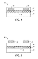
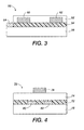
- FIG. 1 to 4 Illustrated in Figures 1 to 4 are various representative embodiments of the present disclosure, and wherein polymers like functionalized heteroacenes are selected as the channel or semiconductor material in thin film transistor (TFT) configurations.
- TFT thin film transistor
- Another feature of the present disclosure resides in providing electronic devices, such as TFTs, with a functionalized heteroacene channel layer, and which layer has a conductivity of from about 10 -4 to about 10 -9 S/cm (Siemens/centimeter).
- novel polymers like functionalized heteroacenes and devices thereof, and which devices exhibit enhanced resistance to the adverse effects of oxygen that is, these devices exhibit relatively high current on/off ratios, and their performance does not substantially degrade as rapidly as similar devices fabricated with regioregular poly(3-alkylthiophene-3,5-diyl) or with heteroacenes.
- R represents a suitable hydrocarbon like alkyl, aryl, or heteroaryl
- each R 1 and R 2 is independently hydrogen (H), a suitable hydrocarbon
- R 3 and R 4 are independently a suitable hydrocarbon, a heteroatom containing group, or a halogen
- x and y represent the number of groups
- Z represents sulfur, oxygen, selenium, or NR' wherein R' is hydrogen, alkyl, or aryl
- m and n each represent the number of rings, such as for example from zero (0) to about 3
- x and y can be, for example, from zero to about 12, and more specifically, wherein each x and y are from about 3 to about 7.
- alkyl with, for example, from about 1 to about 30, including from about 4 to about 18 carbon atoms (included throughout are numbers within the range, for example 4, 5, 6, 7, 8, 9, 10, 11, 12, 13, 14, 15, 16, 17 and 18), and further including from about 6 to about 16 carbon atoms are butyl, pentyl, hexyl, heptyl, octyl, nonyl, decyl, undecyl, dodecyl, tridecyl, tetradecyl, pentadecyl, hexadecyl, heptadecyl, octadecyl, nonadecyl, or eicosanyl, isomeric forms thereof, mixtures thereof, and the like; alkylaryl with from about 7 to about 49 carbon atoms, from about 6 to about 37 carbon atoms, from about 13 to about 25 carbon atoms, such as methyl phenyl, substituted phenyls, and the
- Heteroatom containing groups include, for example, polyethers, trialkylsilyls, heteroaryls, and the like; and more specifically, thienyl, furyl and pyridiaryl.
- the hetero component can be selected from a number of known atoms like sulfur, oxygen, nitrogen, silicon, selenium, and the like.
- R can be an unbranched alkyl of, for example, from about 2 to about 16 carbon atoms; an unbranched alkylaryl where alkyl contains, for example, from about 4 to about 12 carbon atoms; R 1 and R 12 are hydrogen, alkyl, aryl, halogen, cyano, nitro, and the like; m and n are each zero, or from 1 to about 3; and x and y are each zero, or from 1 to about 12.
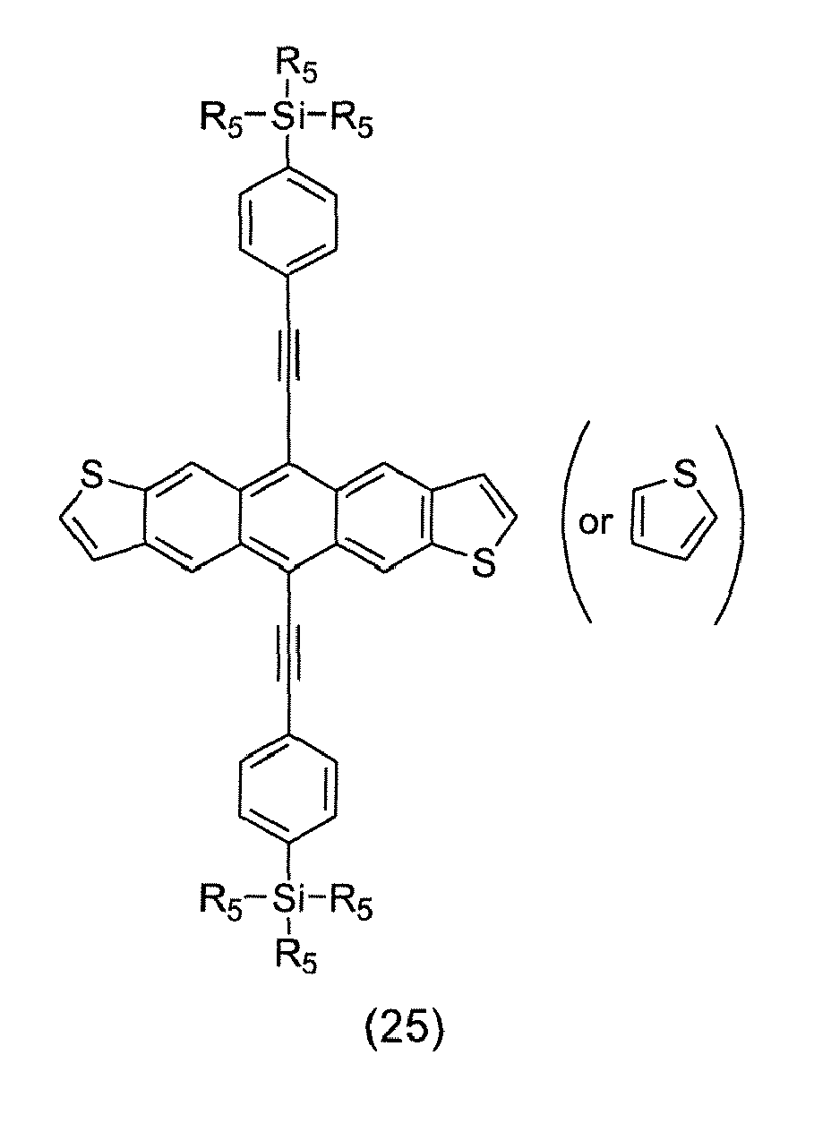
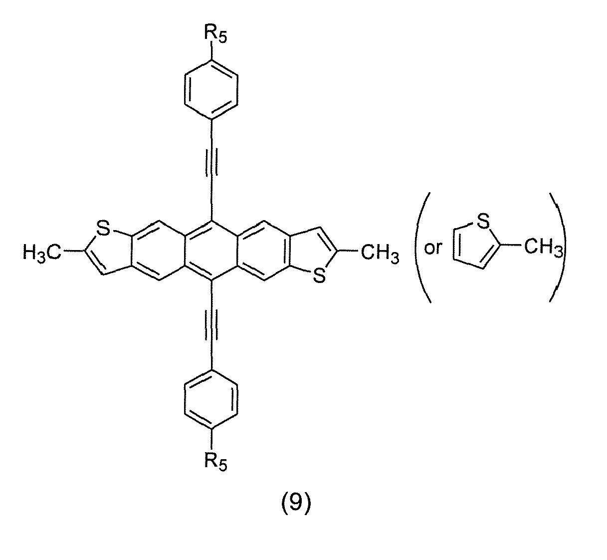
- Hydrocarbons are known and include alkyl, alkoxy, aryl, alkylaryl, substituted alkyl, alkoxy, aryl, and the like. Specific illustrative examples are wherein R 5 is, for example, a hydrocarbon of methyl, ethyl, propyl, butyl, pentyl, hexyl, heptyl, octyl, nonyl, decyl, undecyl, dodecyl, tridecyl, tetradecyl, pentadecyl, hexadecyl, heptadecyl, or octadecyl; trifluoromethyl, fluoroethyl, perfluoropropyl, perfluorobutyl, perfluoropentyl, perfluorohexyl, perfluoroheptyl, perfluorooctyl, perfluorononyl, perfluoro
- the polymers such as the functionalized heteroacenes, in embodiments are soluble or substantially soluble in common coating solvents, for example, in embodiments they possess a solubility of at least about 0.1 percent by weight, and more specifically, from about 10 percent to about 95 percent by weight in such solvents as methylene chloride, 1,2-dichloroethane, tetrahydrofuran, toluene, xylene, mesitylene, chlorobenzene, dichlorobenzene, and the like.
- the functionalized heteroacenes of the present disclosure in embodiments when fabricated as semiconductor channel layers in TFT devices provide a stable conductivity of, for example, from about 10 -9 S/cm to about 10 -4 S/cm, and more specifically, from about 10 -8 S/cm to about 10 -5 S/cm as determined by conventional four-probe conductivity measurements.
- the polymers when fabricated from solutions as thin films are more stable in ambient conditions than similar devices fabricated from heteroacenes.
- the aforementioned polymer materials and devices are generally stable for a number of weeks rather than days or hours as is the situation with poly(3-alkylthiophene-2,5-diyl) after exposure to ambient oxygen, thus the devices fabricated from the functionalized heteroacenes in embodiments of the present disclosure can provide higher current on/off ratios, and their performance characteristics do not substantially change as rapidly as that of nonfunctionalized heteroacenes, or than poly(3-alkylthiophene-2,5-diyl) when no rigorous procedural precautions have been taken to exclude ambient oxygen during material preparation, device fabrication, and evaluation.
- the functionalized heteroacenes stability of the present disclosure in embodiments against oxidative doping, particularly for low cost device manufacturing, does not usually have to be handled in an inert atmosphere, and the processes thereof are, therefore, simpler and more cost effective, and the fabrication thereof can be applied to large scale production processes.
- 1-decyne available from Sigma-Aldrich
- isopropylmagnesium chloride available from Sigma-Aldrich
- THF tetrahydrofuran
- anthra[2,3-b:6,7-b']dithiophene-5,11-dione/anthra[2,3-b:7,6-b]dithiophene-5,11-dione a mixture of trans and cis isomers
- an electronic device containing the functionalized heteroacenes illustrated herein a device which is a thin film transistor comprised of a substrate, a gate electrode, a gate dielectric layer, a source electrode and a drain electrode, and in contact with the source/drain electrodes and the gate dielectric layer, a semiconductor layer comprised of the functionalized heteroacenes illustrated herein, and more specifically, an electronic device comprising a semiconductive material containing a component of Formula (I) wherein R represents alkyl, aryl, or heteroaryl; each R 1 and R 2 is independently hydrogen (H), a suitable hydrocarbon, a heteroatom containing group or a halogen; R 3 and R 4 are independently a suitable hydrocarbon, a heteroatom containing group, or a halogen; x and y represent the number of groups; Z represents sulfur, oxygen, selenium, or NR' wherein R' is hydrogen, alkyl, or aryl; and n and m represent the number of repeating units;
- R represents alkyl, ary
- At least one of R 1 and R 2 is cyano or nitro.
- at least one of R 3 and R 4 is a hydrocarbon of alkyl.
- at least one of R 3 and R 4 is a hydrocarbon of aryl.
- said heteroatom containing group is dialkylamine, diarylamine, alkoxy, trialkylsilyl or triarylsilyl.
- said heteroatom containing group is thienyl, pyridyl, trialkylsilyl, triarylsilyl, or alkoxyalkoxyaryl.
- R 1 , R 2 , R 3 , R 4 and R 5 is alkyl.
- Z is sulfur, oxygen, or selenium.
- Z is NR' wherein R' is alkyl, or aryl.
- m is a number of from 0 to about 3.
- m is 2.
- m is 1.
- n is a number of from 0 to about 3.
- n is 1 or 2.
- x is a number of from 0 to about 12.
- x is a number of from 0 to about 6, a number of from 0 to about 4; or a number of from 0 to about 2.
- y is a number of from 0 to about 12.
- y is a number of from 0 to about 4, a number of from 0 to about 2, or zero.
- alkyl and said hydrocarbon are ethyl, propyl, butyl, pentyl, hexyl, heptyl, octyl, nonyl, decyl, undecyl, dodecyl, tridecyl, tetradecyl, pentadecyl, hexadecyl, heptadecyl, octadecyl, nonadecyl, or eicosanyl.
- aryl and said hydrocarbon are phenyl, tolyl, butylphenyl, pentylphenyl, hexylphenyl, heptylphenyl, octylphenyl, nonylphenyl, decylphenyl, undecylphenyl, dodecylphenyl, tridecylphenyl, tetradecylphenyl, pentadecylphenyl, hexadecylphenyl, heptadecylphenyl, octadecylphenyl, naphthyl, methylnaphthyl, ethylnaphthyl, propylnaphthyl, butylnaphthyl, pentylnaphthyl, hexylnaphthyl, heptylnaphthyl,
- heteroaryl is thienyl, methylthienyl, ethylthienyl, propylthienyl, butylthienyl, hexylthienyl, heptylthienyl, octylthienyl, nonylthienyl, decylthienyl, undecylthienyl, dodecylthienyl, bithiophenyl, methylbithiophenyl, ethylbithiophenyl, propylbithiophenyl, propylbithiophenyl, butylbithiophenyl, pentylbithiophenyl, hexylbithiophenyl, heptylbithiophenyl, octylbithiophenyl, nonylbithiophenyl, decylbithiophenyl, undec
- said substrate is a plastic sheet of a polyester, a polycarbonate, or a polyimide; said gate source and drain electrodes are each independently comprised of silver, gold, nickel, aluminum, chromium, platinum, or indium titanium oxide, or a conductive polymer, and said gate dielectric layer is comprised of inorganic nitrides or oxides, or organic polymers, silicon nitride, silicon oxide, and said component is a functionalized heteroacene and is deposited by solution processes of spin coating, stamp printing, screen printing, or ink jet printing. In a further embodiment said component is a functionalized heteroacene comprised of a mixture of the cis and trans isomers of said formulas.
- At least one of said hydrocarbons is alkyl, aryl, a substituted alkyl, or a substituted aryl.
- said substrate is a plastic sheet of a polyester, a polycarbonate, or a polyimide; said gate source and drain electrodes are each independently comprised of silver, gold, nickel, aluminum, chromium, platinum, or indium titanium oxide, or a conductive polymer, and said gate dielectric layer is comprised of inorganic nitrides or oxides, organic polymers, or silicon nitride, silicon oxide; and said substrate is glass or a plastic sheet; said gate, source and drain electrodes are each comprised of silver, gold, or chromium, and said gate dielectric layer is comprised of the poly(methacrylate), polysiloxane, or poly(vinyl phenol); and optionally wherein said semiconductor layer is 5,11-decynylanthra[2,3-b:6,7-b']dithiophene
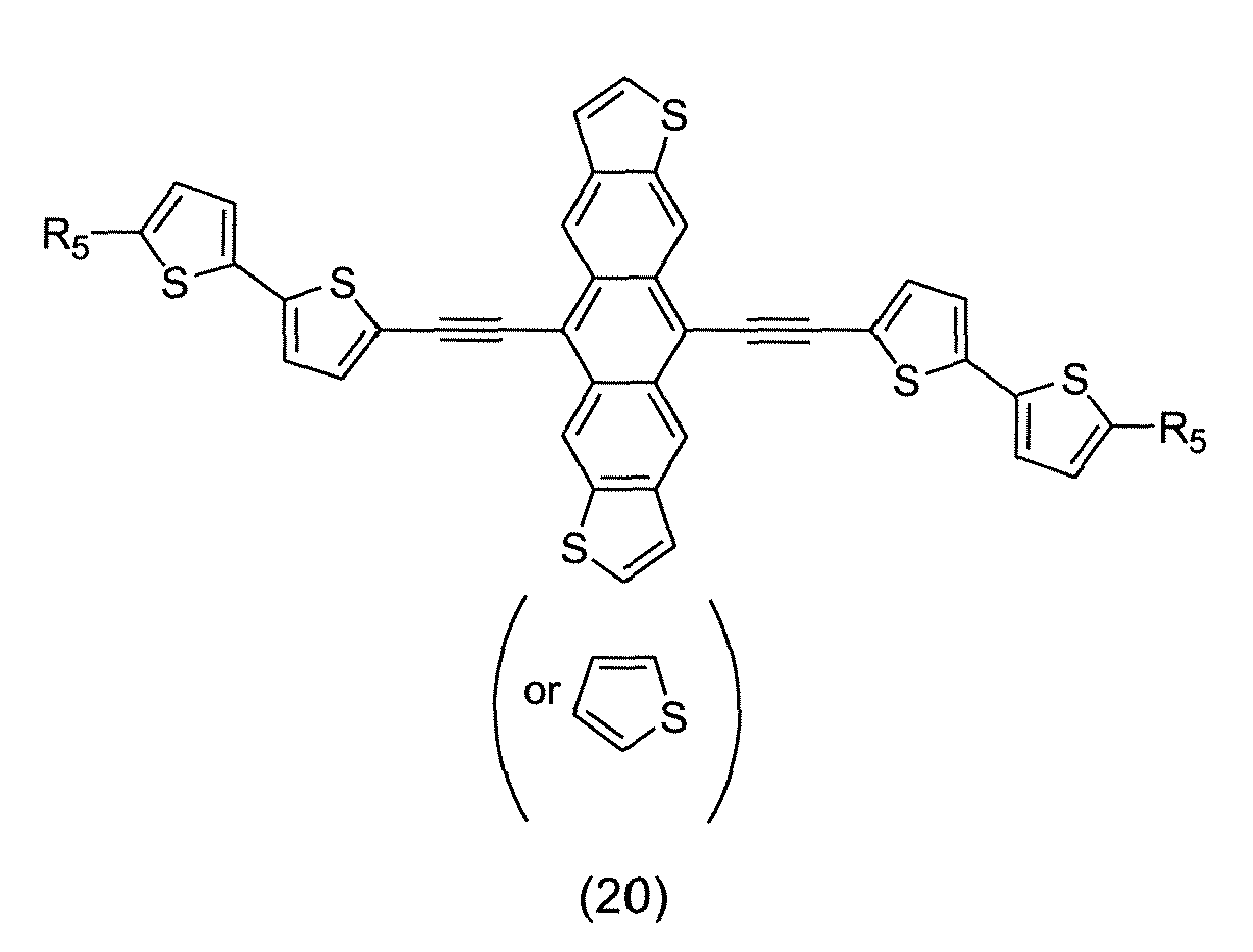
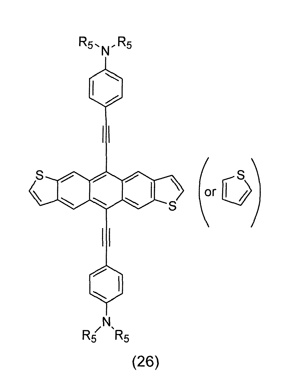
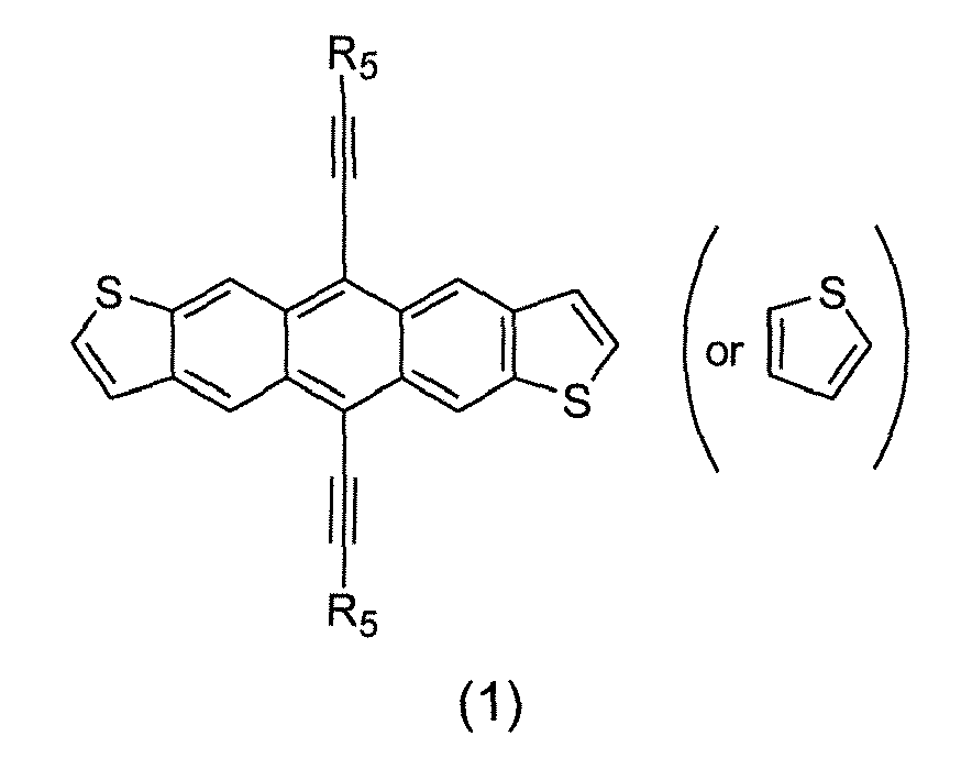
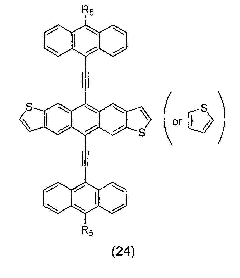
- said semiconductor layer is a functionalized heteroacene is of the following formulas wherein R 5 is methyl, ethyl, propyl, butyl, pentyl, hexyl, heptyl, octyl, nonyl, decyl, undecyl, dodecyl, tridecyl, tetradecyl, pentadecyl, hexadecyl, heptadecyl, or octadecyl; trifluoromethyl, fluoroethyl, perfluoropropyl, perfluorobutyl, perfluoropentyl, perfluorohexyl, perfluoroheptyl, perfluorooctyl, perfluorononyl, perfluorodecyl, perfluoroundecyl, or perfluorododecyl; phenyl, methylphenyl (
- FIG. 1 there is schematically illustrated a TFT configuration 10 comprised of a substrate 16, in contact therewith a metal contact 18 (gate electrode), and a layer of an insulating dielectric layer 14 with the gate electrode having a portion thereof or the entire gate in contact with the dielectric layer 14 on top of which layer 14 two metal contacts, 20 and 22 (source and drain electrodes), are deposited.
- a metal contact 18 gate electrode
- a layer of an insulating dielectric layer 14 with the gate electrode having a portion thereof or the entire gate in contact with the dielectric layer 14 on top of which layer 14 two metal contacts, 20 and 22 (source and drain electrodes), are deposited.
- the polymer layer 12 Over and between the metal contacts 20 and 22 is the polymer layer 12 of 5,11-decynylanthra[2,3-b:6,7-b']dithiophene/5,11-decynylanthra[2,3-b:7,6-b']dithiophene (1a), a mixture of the
- FIG. 2 schematically illustrates another TFT configuration 30 comprised of a substrate 36, a gate electrode 38, a source electrode 40, and a drain electrode 42, an insulating dielectric layer 34, and a functionalized heteroacene semiconductor layer 32 of 5,11-bis(4-phenylethynyl)anthra[2,3-b:6,7-b']dithiophene/5,11-bis(4-phenylethynyl)anthra[2,3-b:7,6-b']dithiophene (8a), a mixture of the cis and trans isomers thereof.
- FIG 3 schematically illustrates a further TFT configuration 50 comprised of a heavily n-doped silicon wafer 56, which can act as a gate electrode, a thermally grown silicon oxide dielectric layer 54, the functionalized heteroacene semiconductor layer 52 of Figure 2, on top of which are deposited a source electrode 60 and a drain electrode 62; and a gate electrode contact 64.
- FIG. 4 schematically illustrates a TFT configuration 70 comprised of substrate 76, a gate electrode 78, a source electrode 80, a drain electrode 82, a functionalized heteroacene semiconductor layer 72 of Figure 2, and an insulating dielectric layer 74.
- TFT devices are envisioned, reference for example known TFT devices.
- an optional protecting layer may be incorporated on top of each of the transistor configurations of Figures 1, 2, 3 and 4.
- the insulating dielectric layer 74 may also function as a protecting layer.
- the device substrate layer may generally be a silicon material inclusive of various appropriate forms of silicon, a glass plate, a plastic film or a sheet, and the like depending on the intended applications.
- a plastic substrate such as for example polyester, polycarbonate, polyimide sheets, and the like, may be selected.
- the thickness of the substrate may be, for example, from about 10 micrometers to over 10 millimeters with a specific thickness being from about 50 to about 100 micrometers, especially for a flexible plastic substrate, and from about 1 to about 10 millimeters for a rigid substrate, such as glass or silicon.
- the insulating dielectric layer which can separate the gate electrode from the source and drain electrodes, and in contact with the semiconductor layer, can generally be an inorganic material film, an organic polymer film, or an organic-inorganic composite film.
- the thickness of the dielectric layer is, for example, from about 10 nanometers to about 1 micrometer with a more specific thickness being about 100 nanometers to about 500 nanometers.
- Illustrative examples of inorganic materials suitable as the dielectric layer include silicon oxide, silicon nitride, aluminum oxide, barium titanate, barium zirconate titanate, and the like; illustrative examples of organic polymers for the dielectric layer include polyesters, polycarbonates, poly(vinyl phenol), polyimides, polystyrene, poly(methacrylate)s, poly(acrylate)s, epoxy resin, and the like; and illustrative examples of inorganic-organic composite materials include nanosized metal oxide particles dispersed in polymers such as polyester, polyimide, epoxy resin and the like.
- the insulating dielectric layer is generally of a thickness of from about 50 nanometers to about 500 nanometers depending on the dielectric constant of the dielectric material used. More specifically, the dielectric material has a dielectric constant of, for example, at least about 3, thus a suitable dielectric thickness of about 300 nanometers can provide a desirable capacitance, for example, of about 10 -9 to about 10 -7 F/cm 2 .
- the active semiconductor layer comprised of the functionalized heteroacenes illustrated herein, and wherein the thickness of this layer is generally, for example, about 10 nanometers to about 1 micrometer, or about 40 to about 100 nanometers.
- This layer can generally be fabricated by solution processes, such as spin coating, casting, screen, stamp, or jet printing of a solution of the functionalized heteroacenes of the present disclosure.
- the gate electrode can be a thin metal film, a conducting polymer film, a conducting film generated from a conducting ink or paste, or the substrate itself (for example, heavily doped silicon).
- gate electrode materials include but are not limited to aluminum, gold, chromium, indium tin oxide, conducting polymers, such as polystyrene sulfonate-doped poly(3,4-ethylenedioxythiophene) (PSS/PEDOT), a conducting ink/paste comprised of carbon black/graphite or colloidal silver dispersion contained in a polymer binder, such as Electrodag available from Acheson Colloids Company, and silver filled electrically conductive thermoplastic ink available from Noelle Industries, and the like.
- the gate layer can be prepared by vacuum evaporation, sputtering of metals or conductive metal oxides, coating from conducting polymer solutions or conducting inks, or dispersions by spin coating, casting or printing.
- the thickness of the gate electrode layer is, for example, from about 10 nanometers to about 10 micrometers, and a specific thickness is, for example, from about 10 to about 200 nanometers for metal films, and about 1 to about 10 micrometers for polymer conductors.
- the source and drain electrode layer can be fabricated from materials which provide a low resistance ohmic contact to the semiconductor layer.
- Typical materials suitable for use as source and drain electrodes include those of the gate electrode materials, such as gold, nickel, aluminum, platinum, conducting polymers, and conducting inks.
- Typical thickness of this layer is, for example, from about 40 nanometers to about 1 micrometer with the more specific thickness being about 100 to about 400 nanometers.
- the TFT devices contain a semiconductor channel with a width W and length L.
- the semiconductor channel width may be, for example, from about 10 micrometers to about 5 millimeters with a specific channel width being about 100 micrometers to about 1 millimeter.
- the semiconductor channel length may be, for example, from about 1 micrometer to about 1 millimeter with a more specific channel length being from about 5 micrometers to about 100 micrometers.
- the source electrode is grounded and a bias voltage of generally, for example, about 0 volt to about -80 volts is applied to the drain electrode to collect the charge carriers transported across the semiconductor channel when a voltage of generally about +10 volts to about -80 volts is applied to the gate electrode.
- alkynyl like the ethynyl groups function primarily to minimize or avoid instability because of exposure to oxygen, and thus increase the oxidative stability of the heteroacenes in solution under ambient conditions, and the alkyl and/or alkylaryl substituents or groups permit the solubility of these compounds in common solvents, such as ethylene chloride.
- alkyl groups that are unbranched could facilitate the formation of layered pi-stacks, a favorable form for charge transport properties.
Landscapes
- Chemical & Material Sciences (AREA)
- Organic Chemistry (AREA)
- Engineering & Computer Science (AREA)
- Materials Engineering (AREA)
- Physics & Mathematics (AREA)
- Spectroscopy & Molecular Physics (AREA)
- Thin Film Transistor (AREA)
- Electroluminescent Light Sources (AREA)
- Nitrogen And Oxygen Or Sulfur-Condensed Heterocyclic Ring Systems (AREA)
Abstract

Description
- The present disclosure is generally directed to polymers and uses thereof. More specifically, the present disclosure in embodiments is directed to a class of heteroacenes functionalized with, for example, alkylethynyl or alkylarylethynyl groups, and other suitable groups as illustrated herein, and which components can be selected as solution processable and substantially stable channel semiconductors in organic electronic devices, such as thin film transistors.
- There are desired electronic devices, such as thin film transistors, TFTs, fabricated with the polymers illustrated herein, such as functionalized heteroacenes with excellent solvent solubility, which can be solution processable; and devices with mechanical durability and structural flexibility, which may be highly desirable for fabricating flexible TFTs on plastic substrates. Flexible TFTs would enable the design of electronic devices which usually involve structural flexibility and mechanical durability characteristics. The use of plastic substrates together with the functionalized heteroacene components can transform the traditionally rigid silicon TFT into a mechanically more durable and structurally flexible TFT design. This is of particular value to large area devices, such as large-area image sensors, electronic paper and other display media. Also, the selection of functionalized heteroacenes TFTs for integrated circuit logic elements for low end microelectronics, such as smart cards, radio frequency identification (RFID) tags, and memory/storage devices, may enhance their mechanical durability, and thus their useful life span.
- A number of semiconductor materials are not, it is believed, stable when exposed to air as they become oxidatively doped by ambient oxygen, resulting in increased conductivity. The result is a large off-current and thus a low current on/off ratio for the devices fabricated from these materials. Accordingly, with many of these materials, rigorous precautions are usually undertaken during materials processing and device fabrication to exclude environmental oxygen to avoid or minimize oxidative doping. These precautionary measures increase the cost of manufacturing therefore offsetting the appeal of certain semiconductor TFTs as an economical alternative to amorphous silicon technology, particularly for large area devices. These and other disadvantages are avoided or minimized in embodiments of the present disclosure.
- Heteroacenes are known to possess acceptable high field effect mobility when used as channel semiconductors in TFTs. However, these materials are rapidly oxidized by, for example, atmospheric oxygen under light, and such materials are not considered processable at ambient conditions. Furthermore, heteroacenes, when selected for TFTs, have poor thin film formation characteristics, and are substantially insoluble or have minimal solubility in a number of commonly used solvents rendering these compounds as being nonsolution processing; accordingly, such compounds have been mostly processed by vacuum deposition methods that result in high production costs, and which disadvantages are eliminated or minimized with the TFTs generated with the functionalized heterocenes illustrated herein.
- A number of organic semiconductor materials has been described for use in field effect TFTs, which materials include organic small molecules such as pentacene, see for example D.J. Gundlach et al., "Pentacene organic thin film transistors - molecular ordering and mobility", IEEE Electron Device Lett., Vol. 18, p. 87 (1997 ); oligomers, such as sexithiophenes or their variants, see for example reference F. Garnier et al., "Molecular engineering of organic semiconductors: Design of self-assembly properties in conjugated thiophene oligomers", J. Amer. Chem. Soc., Vol. 115, p. 8716 (1993 ), and certain functionalized heteroacenes, such as poly(3-alkylthiophene), see for example reference Z. Bao et al., "Soluble and processable regioregular poly(3-hexylthiophene) for field-effect thin film transistor application with high mobility", Appl. Phys. Lett. Vol. 69, p4108 (1996 ). Although organic material based TFTs generally provide lower performance characteristics than their conventional silicon counterparts, such as silicon crystal or polysilicon TFTs, they may nonetheless be sufficiently useful for applications in areas where high mobility is not required. These devices may include large area devices, such as image sensors, active matrix liquid crystal displays and low end microelectronics, such as smart cards and RFID tags.
- TFTs fabricated from the polymers illustrated herein, such as functionalized heteroacenes, may be functionally and structurally more desirable than conventional silicon technology in that they may offer mechanical durability, while also avoiding vacuum deposition, structural flexibility, and the potential of being able to be incorporated directly onto the active media of the devices thus enhancing device compactness for transportability.
- With vacuum deposition, it is difficult to achieve consistent thin film quality for large area formats. Polymer TFTs, such as those fabricated from regioregular components, of, for example, regioregular poly(3-alkylthiophene-2,5-diyl) by solution processes, while offering some mobility, suffer from their propensity toward oxidative doping in air. For practical low cost TFT design, it is therefore of value to have a semiconductor material that is both stable and solution processable, and where its performance is not adversely affected by ambient oxygen, for example, TFTs generated with poly(3-alkylthiophene-2,5-diyl) are very sensitive to air. The TFTs fabricated from these materials in ambient conditions generally exhibit very large off-current, very low current on/off ratios, and their performance characteristics degrade rapidly.
- Illustrated in Figures 1 to 4 are various representative embodiments of the present disclosure, and wherein polymers like functionalized heteroacenes are selected as the channel or semiconductor material in thin film transistor (TFT) configurations.
- It is a feature of the present disclosure to provide polymer semiconductors, which are useful in microelectronic device applications, such as TFT devices.
- It is another feature of the present disclosure to provide functionalized heteroacenes with a band gap of from about 1.5 eV to about 3 eV as determined from the absorption spectra of thin films thereof, and which functionalized heteroacenes are suitable for use as TFT semiconductor channel layer materials.
- In yet a further feature of the present disclosure there are provided functionalized heteroacenes which are useful as microelectronic components, and which functionalized heteroacenes possess solubility of, for example, at least about 0.1 percent to about 95 percent by weight in common organic solvents, such as methylene chloride, tetrahydrofuran, toluene, xylene, mesitylene, chlorobenzene, and the like, and thus these components can be economically fabricated by solution processes such as spin coating, screen printing, stamp printing, dip coating, solution casting, jet printing, and the like.
- Another feature of the present disclosure resides in providing electronic devices, such as TFTs, with a functionalized heteroacene channel layer, and which layer has a conductivity of from about 10-4 to about 10-9 S/cm (Siemens/centimeter).
- Also, in yet another feature of the present disclosure there are provided novel polymers like functionalized heteroacenes and devices thereof, and which devices exhibit enhanced resistance to the adverse effects of oxygen, that is, these devices exhibit relatively high current on/off ratios, and their performance does not substantially degrade as rapidly as similar devices fabricated with regioregular poly(3-alkylthiophene-3,5-diyl) or with heteroacenes.
- Additionally, in a further feature of the present disclosure there is provided a class of novel polymers like functionalized heteroacenes with unique structural features, which are conducive to molecular self-alignment under appropriate processing conditions, and which structural features also enhance the stability of device performance. Proper molecular alignment can permit higher molecular structural order in thin films, which can be important to efficient charge carrier transport, thus higher electrical performance.
- There are disclosed in the embodiments, polymers like functionalized heteroacenes and electronic devices thereof. More specifically, the present disclosure relates to polymers illustrated by or encompassed by Formula (I)

- Examples of alkyl with, for example, from about 1 to about 30, including from about 4 to about 18 carbon atoms (included throughout are numbers within the range, for example 4, 5, 6, 7, 8, 9, 10, 11, 12, 13, 14, 15, 16, 17 and 18), and further including from about 6 to about 16 carbon atoms are butyl, pentyl, hexyl, heptyl, octyl, nonyl, decyl, undecyl, dodecyl, tridecyl, tetradecyl, pentadecyl, hexadecyl, heptadecyl, octadecyl, nonadecyl, or eicosanyl, isomeric forms thereof, mixtures thereof, and the like; alkylaryl with from about 7 to about 49 carbon atoms, from about 6 to about 37 carbon atoms, from about 13 to about 25 carbon atoms, such as methyl phenyl, substituted phenyls, and the like; or aryl, such as phenyl with about 6 to about 48 carbon atoms.
- Heteroatom containing groups include, for example, polyethers, trialkylsilyls, heteroaryls, and the like; and more specifically, thienyl, furyl and pyridiaryl. The hetero component can be selected from a number of known atoms like sulfur, oxygen, nitrogen, silicon, selenium, and the like.
- In embodiments, R can be an unbranched alkyl of, for example, from about 2 to about 16 carbon atoms; an unbranched alkylaryl where alkyl contains, for example, from about 4 to about 12 carbon atoms; R1 and R12 are hydrogen, alkyl, aryl, halogen, cyano, nitro, and the like; m and n are each zero, or from 1 to about 3; and x and y are each zero, or from 1 to about 12.
- Hydrocarbons are known and include alkyl, alkoxy, aryl, alkylaryl, substituted alkyl, alkoxy, aryl, and the like. Specific illustrative examples are




- The polymers, such as the functionalized heteroacenes, in embodiments are soluble or substantially soluble in common coating solvents, for example, in embodiments they possess a solubility of at least about 0.1 percent by weight, and more specifically, from about 10 percent to about 95 percent by weight in such solvents as methylene chloride, 1,2-dichloroethane, tetrahydrofuran, toluene, xylene, mesitylene, chlorobenzene, dichlorobenzene, and the like. Moreover, the functionalized heteroacenes of the present disclosure in embodiments when fabricated as semiconductor channel layers in TFT devices provide a stable conductivity of, for example, from about 10-9 S/cm to about 10-4 S/cm, and more specifically, from about 10-8 S/cm to about 10-5 S/cm as determined by conventional four-probe conductivity measurements.
- It is believed that the polymers when fabricated from solutions as thin films, for example, of from about 10 nanometers to about 500 nanometers or from about 100 to about 300 nanometers in thickness materials are more stable in ambient conditions than similar devices fabricated from heteroacenes. When unprotected, the aforementioned polymer materials and devices are generally stable for a number of weeks rather than days or hours as is the situation with poly(3-alkylthiophene-2,5-diyl) after exposure to ambient oxygen, thus the devices fabricated from the functionalized heteroacenes in embodiments of the present disclosure can provide higher current on/off ratios, and their performance characteristics do not substantially change as rapidly as that of nonfunctionalized heteroacenes, or than poly(3-alkylthiophene-2,5-diyl) when no rigorous procedural precautions have been taken to exclude ambient oxygen during material preparation, device fabrication, and evaluation. The functionalized heteroacenes stability of the present disclosure in embodiments against oxidative doping, particularly for low cost device manufacturing, does not usually have to be handled in an inert atmosphere, and the processes thereof are, therefore, simpler and more cost effective, and the fabrication thereof can be applied to large scale production processes.
- The preparation of functionalized heteroacenes of the present disclosure can be generally accomplished as illustrated herein. More specifically, one process of preparation is illustrated in Scheme 1.

- 5,11-Decynylanthra[2,3-b:6,7-b']dithiophene/5,11-decynylanthra[2,3-b:7,6-b']dithiophene (1a, a mixture of trans and cis isomers) and 5,11-bis(4-phenylethynyl)anthra[2,3-b:6,7-b']dithiophene/5,11-bis(4-phenylethynyl)anthra[2,3-b:7,6-b']dithiophene (8a, a mixture of trans and cis isomers) can be generated as shown in Scheme 1. First, 1-decyne (available from Sigma-Aldrich) is reacted with about 1 molar equivalent of isopropylmagnesium chloride (available from Sigma-Aldrich) in tetrahydrofuran (THF) at elevated temperatures of, for example, 60°C for a suitable period like 30 minutes. Then to the reaction mixture is added anthra[2,3-b:6,7-b']dithiophene-5,11-dione/anthra[2,3-b:7,6-b]dithiophene-5,11-dione (a mixture of trans and cis isomers) (this starting material is prepared according to De la Cruz, P., et al, J. Org. Chem. 1992, 57, 6192 ) followed by stirring at elevated temperatures of, for example, 60°C for a suitable period like 1 hour. Finally, tin (II) chloride (SnCl2) solution in 10 percent HCl is added to the reaction mixture and stirred at elevated temperatures of, for example, 60°C for a suitable period like 30 minutes. After work up and recrystallization, the substantially pure compound 1 a is obtained. Compound 8a is prepared similarly starting from 1-ethynyl-4-pentylbenzene (available from Sigma-Aldrich) instead of 1-decyne.
- Aspects of the present disclosure relate to an electronic device containing the functionalized heteroacenes illustrated herein; a device which is a thin film transistor comprised of a substrate, a gate electrode, a gate dielectric layer, a source electrode and a drain electrode, and in contact with the source/drain electrodes and the gate dielectric layer, a semiconductor layer comprised of the functionalized heteroacenes illustrated herein, and more specifically, an electronic device comprising a semiconductive material containing a component of Formula (I)








- In one embodiment of the device in accordance with claim 1, at least one of R1 and R2 is cyano or nitro.
In a further embodiment at least one of R3 and R4 is a hydrocarbon of alkyl.
In a further embodiment at least one of R3 and R4 is a hydrocarbon of aryl.
In a further embodiment said heteroatom containing group is dialkylamine, diarylamine, alkoxy, trialkylsilyl or triarylsilyl.
In a further embodiment said heteroatom containing group is thienyl, pyridyl, trialkylsilyl, triarylsilyl, or alkoxyalkoxyaryl.
In a further embodiment at least one of R1, R2, R3, R4 and R5 is alkyl.
In a further embodiment Z is sulfur, oxygen, or selenium.
In a further embodiment Z is NR' wherein R' is alkyl, or aryl.
In a further embodiment m is a number of from 0 to about 3.
In a further embodiment m is 2.
In a further embodiment m is 1.
In a further embodiment n is a number of from 0 to about 3.
In a further embodiment n is 1 or 2.
In a further embodiment x is a number of from 0 to about 12.
In a further embodiment x is a number of from 0 to about 6, a number of from 0 to about 4; or a number of from 0 to about 2.
In a further embodiment y is a number of from 0 to about 12.
In a further embodiment y is a number of from 0 to about 4, a number of from 0 to about 2, or zero.
In a further embodiment R is aryl with 6 to about 36 carbon atoms; R1 and R2 are hydrogen; and m=n=1;x=y=0; or wherein m = n = 2; x = y = 0. - In one embodiment of the transistor of claim 9, alkyl and said hydrocarbon are ethyl, propyl, butyl, pentyl, hexyl, heptyl, octyl, nonyl, decyl, undecyl, dodecyl, tridecyl, tetradecyl, pentadecyl, hexadecyl, heptadecyl, octadecyl, nonadecyl, or eicosanyl.
In a further embodiment aryl and said hydrocarbon are phenyl, tolyl, butylphenyl, pentylphenyl, hexylphenyl, heptylphenyl, octylphenyl, nonylphenyl, decylphenyl, undecylphenyl, dodecylphenyl, tridecylphenyl, tetradecylphenyl, pentadecylphenyl, hexadecylphenyl, heptadecylphenyl, octadecylphenyl, naphthyl, methylnaphthyl, ethylnaphthyl, propylnaphthyl, butylnaphthyl, pentylnaphthyl, hexylnaphthyl, heptylnaphthyl, octylnaphthyl, nonylnaphthyl, decylnaphthyl, undecylnaphthyl, dodecylnaphthyl, anthryl, methylanthryl, ethylanthryl, propylanthryl, butylanthyl, pentylanthryl, octylanthryl, nonylanthryl, decylanthryl, undecylanthryl, or dodecylanthryl.
In a further embodiment heteroaryl is thienyl, methylthienyl, ethylthienyl, propylthienyl, butylthienyl, hexylthienyl, heptylthienyl, octylthienyl, nonylthienyl, decylthienyl, undecylthienyl, dodecylthienyl, bithiophenyl, methylbithiophenyl, ethylbithiophenyl, propylbithiophenyl, propylbithiophenyl, butylbithiophenyl, pentylbithiophenyl, hexylbithiophenyl, heptylbithiophenyl, octylbithiophenyl, nonylbithiophenyl, decylbithiophenyl, undecylbithiophenyl, dodecylbithiophenyl, pyridyl, methylpyridyl, ethylpyridyl, propylpyridyl, butylpyridyl, pentylpyridyl, hexylpyridyl, heptylpyridyl, octylpyridyl, nonylpyridyl, decylpyridyl, undecylpyridyl, dodecylpyridyl, thiazolyl, methylthiazolyl, ethylthiazolyl, propylthiazolyl, butylthiazolyl, pentylthiazolyl, hexylthiazolyl, heptylthiazolyl, octylthiazolyl, nonylthiazolyl, decylthiazolyl, undecylthiazolyl, or dodecylthiazolyl.
In one embodiment of the devices ofclaims 9 and 10, said substrate is a plastic sheet of a polyester, a polycarbonate, or a polyimide; said gate source and drain electrodes are each independently comprised of silver, gold, nickel, aluminum, chromium, platinum, or indium titanium oxide, or a conductive polymer, and said gate dielectric layer is comprised of inorganic nitrides or oxides, or organic polymers, silicon nitride, silicon oxide, and said component is a functionalized heteroacene and is deposited by solution processes of spin coating, stamp printing, screen printing, or ink jet printing.
In a further embodiment said component is a functionalized heteroacene comprised of a mixture of the cis and trans isomers of said formulas.
In a further embodiment at least one of said hydrocarbons is alkyl, aryl, a substituted alkyl, or a substituted aryl.
In a further embodiment said substrate is a plastic sheet of a polyester, a polycarbonate, or a polyimide; said gate source and drain electrodes are each independently comprised of silver, gold, nickel, aluminum, chromium, platinum, or indium titanium oxide, or a conductive polymer, and said gate dielectric layer is comprised of inorganic nitrides or oxides, organic polymers, or silicon nitride, silicon oxide; and said substrate is glass or a plastic sheet; said gate, source and drain electrodes are each comprised of silver, gold, or chromium, and said gate dielectric layer is comprised of the poly(methacrylate), polysiloxane, or poly(vinyl phenol); and optionally wherein said semiconductor layer is 5,11-decynylanthra[2,3-b:6,7-b']dithiophene/5,11-decynylanthra[2,3-b:7,6-b']dithiophene (1a) and 5,11-bis(4-phenylethynyl)anthra[2,3-b:6,7-b']dithiophene/5,11-bis(4-phenylethynyl)anthra[2,3-b:7,6-b']dithiophene (8a), or mixtures of trans and cis isomers thereof.
In a further embodiment, said semiconductor layer is a functionalized heteroacene is of the following formulas


- In Figure 1 there is schematically illustrated a
TFT configuration 10 comprised of asubstrate 16, in contact therewith a metal contact 18 (gate electrode), and a layer of an insulatingdielectric layer 14 with the gate electrode having a portion thereof or the entire gate in contact with thedielectric layer 14 on top of whichlayer 14 two metal contacts, 20 and 22 (source and drain electrodes), are deposited. Over and between themetal contacts polymer layer 12 of 5,11-decynylanthra[2,3-b:6,7-b']dithiophene/5,11-decynylanthra[2,3-b:7,6-b']dithiophene (1a), a mixture of the cis and trans isomers thereof. The gate electrode can be included in the substrate, in the dielectric layer, and the like throughout. - Figure 2 schematically illustrates another
TFT configuration 30 comprised of asubstrate 36, agate electrode 38, asource electrode 40, and adrain electrode 42, an insulatingdielectric layer 34, and a functionalizedheteroacene semiconductor layer 32 of 5,11-bis(4-phenylethynyl)anthra[2,3-b:6,7-b']dithiophene/5,11-bis(4-phenylethynyl)anthra[2,3-b:7,6-b']dithiophene (8a), a mixture of the cis and trans isomers thereof. - Figure 3 schematically illustrates a
further TFT configuration 50 comprised of a heavily n-dopedsilicon wafer 56, which can act as a gate electrode, a thermally grown siliconoxide dielectric layer 54, the functionalizedheteroacene semiconductor layer 52 of Figure 2, on top of which are deposited asource electrode 60 and adrain electrode 62; and agate electrode contact 64. - Figure 4 schematically illustrates a
TFT configuration 70 comprised ofsubstrate 76, agate electrode 78, asource electrode 80, adrain electrode 82, a functionalizedheteroacene semiconductor layer 72 of Figure 2, and an insulatingdielectric layer 74. - Also, other devices not disclosed, especially TFT devices, are envisioned, reference for example known TFT devices.
- In some embodiments of the present disclosure, an optional protecting layer may be incorporated on top of each of the transistor configurations of Figures 1, 2, 3 and 4. For the TFT configuration of Figure 4, the insulating
dielectric layer 74 may also function as a protecting layer. - Also disclosed are semiconductors of thiopheneacenes of the following formula

- These novel organic semiconductors, such as for use in TFTs, can be prepared by the following reaction scheme

- The final product was greenish and it showed a UV maximum peak at a wavelength of 740 nanometers. The UV spectra data for the maximum peak absorbance at 740 nanometers are listed in Table 1. It showed that the solution of structure (2) is more stable in the ambient condition than pentacene.
TABLE 1 UV SPECTRA DATA FOR THE STRUCTURE (2) IN THF Time (Min.) Maximum Wavelength (λ, nm) Absorbance Stability 1 740 1.193 100% 10 740 1.163 97.5% 20 740 1.121 94.0% 30 740 1.080 90.5% - In embodiments and with further reference to the present disclosure and the Figures, the device substrate layer may generally be a silicon material inclusive of various appropriate forms of silicon, a glass plate, a plastic film or a sheet, and the like depending on the intended applications. For structurally flexible devices, a plastic substrate, such as for example polyester, polycarbonate, polyimide sheets, and the like, may be selected. The thickness of the substrate may be, for example, from about 10 micrometers to over 10 millimeters with a specific thickness being from about 50 to about 100 micrometers, especially for a flexible plastic substrate, and from about 1 to about 10 millimeters for a rigid substrate, such as glass or silicon.
- The insulating dielectric layer, which can separate the gate electrode from the source and drain electrodes, and in contact with the semiconductor layer, can generally be an inorganic material film, an organic polymer film, or an organic-inorganic composite film. The thickness of the dielectric layer is, for example, from about 10 nanometers to about 1 micrometer with a more specific thickness being about 100 nanometers to about 500 nanometers. Illustrative examples of inorganic materials suitable as the dielectric layer include silicon oxide, silicon nitride, aluminum oxide, barium titanate, barium zirconate titanate, and the like; illustrative examples of organic polymers for the dielectric layer include polyesters, polycarbonates, poly(vinyl phenol), polyimides, polystyrene, poly(methacrylate)s, poly(acrylate)s, epoxy resin, and the like; and illustrative examples of inorganic-organic composite materials include nanosized metal oxide particles dispersed in polymers such as polyester, polyimide, epoxy resin and the like. The insulating dielectric layer is generally of a thickness of from about 50 nanometers to about 500 nanometers depending on the dielectric constant of the dielectric material used. More specifically, the dielectric material has a dielectric constant of, for example, at least about 3, thus a suitable dielectric thickness of about 300 nanometers can provide a desirable capacitance, for example, of about 10-9 to about 10-7 F/cm2.
- Situated, for example, between and in contact with the dielectric layer and the source/drain electrodes is the active semiconductor layer comprised of the functionalized heteroacenes illustrated herein, and wherein the thickness of this layer is generally, for example, about 10 nanometers to about 1 micrometer, or about 40 to about 100 nanometers. This layer can generally be fabricated by solution processes, such as spin coating, casting, screen, stamp, or jet printing of a solution of the functionalized heteroacenes of the present disclosure.
- The gate electrode can be a thin metal film, a conducting polymer film, a conducting film generated from a conducting ink or paste, or the substrate itself (for example, heavily doped silicon). Examples of gate electrode materials include but are not limited to aluminum, gold, chromium, indium tin oxide, conducting polymers, such as polystyrene sulfonate-doped poly(3,4-ethylenedioxythiophene) (PSS/PEDOT), a conducting ink/paste comprised of carbon black/graphite or colloidal silver dispersion contained in a polymer binder, such as Electrodag available from Acheson Colloids Company, and silver filled electrically conductive thermoplastic ink available from Noelle Industries, and the like. The gate layer can be prepared by vacuum evaporation, sputtering of metals or conductive metal oxides, coating from conducting polymer solutions or conducting inks, or dispersions by spin coating, casting or printing. The thickness of the gate electrode layer is, for example, from about 10 nanometers to about 10 micrometers, and a specific thickness is, for example, from about 10 to about 200 nanometers for metal films, and about 1 to about 10 micrometers for polymer conductors.
- The source and drain electrode layer can be fabricated from materials which provide a low resistance ohmic contact to the semiconductor layer. Typical materials suitable for use as source and drain electrodes include those of the gate electrode materials, such as gold, nickel, aluminum, platinum, conducting polymers, and conducting inks. Typical thickness of this layer is, for example, from about 40 nanometers to about 1 micrometer with the more specific thickness being about 100 to about 400 nanometers. The TFT devices contain a semiconductor channel with a width W and length L. The semiconductor channel width may be, for example, from about 10 micrometers to about 5 millimeters with a specific channel width being about 100 micrometers to about 1 millimeter. The semiconductor channel length may be, for example, from about 1 micrometer to about 1 millimeter with a more specific channel length being from about 5 micrometers to about 100 micrometers.
- The source electrode is grounded and a bias voltage of generally, for example, about 0 volt to about -80 volts is applied to the drain electrode to collect the charge carriers transported across the semiconductor channel when a voltage of generally about +10 volts to about -80 volts is applied to the gate electrode.
- Other known materials not recited herein for the various components of the TFT devices of the present disclosure can also be selected in embodiments.
- Although not desiring to be limited by theory, it is believed that the alkynyl like the ethynyl groups function primarily to minimize or avoid instability because of exposure to oxygen, and thus increase the oxidative stability of the heteroacenes in solution under ambient conditions, and the alkyl and/or alkylaryl substituents or groups permit the solubility of these compounds in common solvents, such as ethylene chloride. Also, in embodiments alkyl groups that are unbranched could facilitate the formation of layered pi-stacks, a favorable form for charge transport properties.
Claims (10)
- An electronic device comprising a semiconductive material containing a component of Formula (I)

- A device in accordance with claim 1 wherein R is aryl with from about 6 to about 48 carbon atoms.
- A device in accordance with claim 1 wherein R is alkyl with from about 1 to about 25 carbon atoms, and wherein two five-membered heteroaromatic moieties are in the trans position, in the cis position, or in both the cis and trans positions.
- A device in accordance with claim 1 wherein R is a heteroaryl with from about 7 to about 37 carbon atoms.
- A device in accordance with claim 1 wherein at least one of R1 and R2 is hydrogen.
- A device in accordance with claim 1 wherein at least one of R1 and R2 is a hydrocarbon of alkyl.
- A device in accordance with claim 1 wherein at least one of R1 and R2 is a hydrocarbon of aryl.
- A device in accordance with claim 1 wherein at least one of R1 and R2 is halogen.
- A thin film transistor comprised of a substrate, a gate electrode, a gate dielectric layer, a source electrode and a drain electrode, and in contact with the source/drain electrodes and the gate dielectric layer a semiconductor layer comprised of components of the formula

- A thin film transistor comprised of a substrate, a gate electrode, a gate dielectric layer, a source electrode, a drain electrode and a layer of a functionalized heteroacene of the formulas/structures




Applications Claiming Priority (1)
| Application Number | Priority Date | Filing Date | Title |
|---|---|---|---|
| US11/398,981 US7372071B2 (en) | 2006-04-06 | 2006-04-06 | Functionalized heteroacenes and electronic devices generated therefrom |
Publications (3)
| Publication Number | Publication Date |
|---|---|
| EP1843410A2 true EP1843410A2 (en) | 2007-10-10 |
| EP1843410A3 EP1843410A3 (en) | 2012-09-12 |
| EP1843410B1 EP1843410B1 (en) | 2013-10-16 |
Family
ID=38179667
Family Applications (1)
| Application Number | Title | Priority Date | Filing Date |
|---|---|---|---|
| EP07105806.9A Active EP1843410B1 (en) | 2006-04-06 | 2007-04-05 | Functionalized heteroacenes and electronic devices generated therefrom |
Country Status (9)
| Country | Link |
|---|---|
| US (1) | US7372071B2 (en) |
| EP (1) | EP1843410B1 (en) |
| JP (1) | JP5307349B2 (en) |
| KR (1) | KR101371041B1 (en) |
| CN (1) | CN101050269B (en) |
| BR (1) | BRPI0701605A (en) |
| CA (1) | CA2583053C (en) |
| MX (1) | MX2007003901A (en) |
| TW (1) | TWI433851B (en) |
Cited By (1)
| Publication number | Priority date | Publication date | Assignee | Title |
|---|---|---|---|---|
| WO2011098113A3 (en) * | 2010-02-15 | 2011-10-06 | Merck Patent Gmbh | Semiconducting polymers |
Families Citing this family (17)
| Publication number | Priority date | Publication date | Assignee | Title |
|---|---|---|---|---|
| US7557370B2 (en) * | 2006-04-06 | 2009-07-07 | Xerox Corporation | Heteroacene polymers and electronic devices generated therefrom |
| US7563860B2 (en) * | 2006-04-06 | 2009-07-21 | Xerox Corporation | Semiconductors and electronic devices generated therefrom |
| CN101495487A (en) * | 2006-07-26 | 2009-07-29 | 默克专利有限公司 | Substituted benzodithiophenes and benzodiselenophenes |
| US20080142793A1 (en) * | 2006-11-10 | 2008-06-19 | Tang Ming L | Organic Semiconductors |
| CN101657458B (en) * | 2007-03-07 | 2014-07-02 | 肯塔基大学研究基金会 | Silylethynylated heteroacenes and electronic devices made therewith |
| US8216753B2 (en) | 2007-12-13 | 2012-07-10 | E I Du Pont De Nemours And Company | Electroactive materials |
| US8212239B2 (en) | 2007-12-13 | 2012-07-03 | E I Du Pont De Nemours And Company | Electroactive materials |
| US8115200B2 (en) * | 2007-12-13 | 2012-02-14 | E.I. Du Pont De Nemours And Company | Electroactive materials |
| US8461291B2 (en) * | 2007-12-17 | 2013-06-11 | E I Du Pont De Nemours And Company | Organic electroactive materials and an organic electronic device having an electroactive layer utilizing the same material |
| US8067764B2 (en) * | 2007-12-17 | 2011-11-29 | E. I. Du Pont De Nemours And Company | Electroactive materials |
| US8425808B2 (en) | 2010-04-27 | 2013-04-23 | Xerox Corporation | Semiconducting composition |
| EP2603499A2 (en) * | 2010-08-13 | 2013-06-19 | Merck Patent GmbH | Anthra[2,3-b:7,6-b']dithiophene derivatives and their use as organic semiconductors |
| GB201203159D0 (en) * | 2012-02-23 | 2012-04-11 | Smartkem Ltd | Organic semiconductor compositions |
| US20150102308A1 (en) * | 2012-04-17 | 2015-04-16 | Sony Corporation | Organic semiconductor layer, electronic device, and method for manufacturing electronic device |
| CN103554138B (en) * | 2013-10-31 | 2016-02-17 | 兰州大学 | A kind of have material of organic field effect tube character and preparation method thereof |
| JP6314807B2 (en) * | 2014-12-08 | 2018-04-25 | 株式会社デンソー | Organic semiconductor device and manufacturing method thereof |
| CN112930586B (en) | 2018-10-31 | 2025-03-28 | 浜松光子学株式会社 | Method for manufacturing semiconductor substrate, method for manufacturing damascene wiring structure, semiconductor substrate and damascene wiring structure |
Family Cites Families (16)
| Publication number | Priority date | Publication date | Assignee | Title |
|---|---|---|---|---|
| US5619357A (en) * | 1995-06-06 | 1997-04-08 | International Business Machines Corporation | Flat panel display containing black matrix polymer |
| US5969376A (en) * | 1996-08-23 | 1999-10-19 | Lucent Technologies Inc. | Organic thin film transistor having a phthalocyanine semiconductor layer |
| US6107117A (en) * | 1996-12-20 | 2000-08-22 | Lucent Technologies Inc. | Method of making an organic thin film transistor |
| JPH10340786A (en) * | 1997-06-09 | 1998-12-22 | Toyo Ink Mfg Co Ltd | Organic electroluminecent element material and organic electroluminescent element using it |
| US5936259A (en) * | 1997-10-16 | 1999-08-10 | Lucent Technologies Inc. | Thin film transistor and organic semiconductor material thereof |
| US5777070A (en) * | 1997-10-23 | 1998-07-07 | The Dow Chemical Company | Process for preparing conjugated polymers |
| US6690029B1 (en) * | 2001-08-24 | 2004-02-10 | University Of Kentucky Research Foundation | Substituted pentacenes and electronic devices made with substituted pentacenes |
| WO2003028125A2 (en) * | 2001-09-27 | 2003-04-03 | 3M Innovative Properties Company | Substituted pentacene semiconductors |
| US6946676B2 (en) * | 2001-11-05 | 2005-09-20 | 3M Innovative Properties Company | Organic thin film transistor with polymeric interface |
| US6949762B2 (en) | 2002-01-11 | 2005-09-27 | Xerox Corporation | Polythiophenes and devices thereof |
| US7250625B2 (en) * | 2002-01-11 | 2007-07-31 | Xerox Corporation | Polythiophenes and electronic devices generated therefrom |
| US6770904B2 (en) * | 2002-01-11 | 2004-08-03 | Xerox Corporation | Polythiophenes and electronic devices generated therefrom |
| DE60305570T2 (en) * | 2002-04-24 | 2007-05-03 | Merck Patent Gmbh | Reactive mesogenic benzodithiophenes |
| ATE475971T1 (en) * | 2003-11-28 | 2010-08-15 | Merck Patent Gmbh | ORGANIC SEMICONDUCTOR LAYER FORMULATIONS WITH POLYACENES AND ORGANIC BINDER POLYMERS |
| JP2005206750A (en) * | 2004-01-26 | 2005-08-04 | Konica Minolta Holdings Inc | Organic semiconductor materials, organic transistors, field effect transistors, switching elements, and 5-membered heterocyclic compounds |
| KR101069519B1 (en) | 2004-07-08 | 2011-09-30 | 삼성전자주식회사 | Organic semiconducting polymer comprising oligothiophene and n-type aromatic compound alternately in the main chain |
-
2006
- 2006-04-06 US US11/398,981 patent/US7372071B2/en not_active Expired - Lifetime
-
2007
- 2007-03-29 CA CA2583053A patent/CA2583053C/en active Active
- 2007-03-30 MX MX2007003901A patent/MX2007003901A/en active IP Right Grant
- 2007-04-04 JP JP2007098064A patent/JP5307349B2/en active Active
- 2007-04-04 TW TW096112011A patent/TWI433851B/en active
- 2007-04-05 CN CN200710089882.3A patent/CN101050269B/en active Active
- 2007-04-05 KR KR1020070033699A patent/KR101371041B1/en active Active
- 2007-04-05 EP EP07105806.9A patent/EP1843410B1/en active Active
- 2007-04-09 BR BRPI0701605-0A patent/BRPI0701605A/en not_active Application Discontinuation
Non-Patent Citations (4)
| Title |
|---|
| D.J. GUNDLACH ET AL.: "Pentacene organic thin film transistors - molecular ordering and mobility", IEEE ELECTRON DEVICE LETT., vol. 18, 1997, pages 87, XP000678864, DOI: doi:10.1109/55.556089 |
| DE LA CRUZ, P. ET AL., J. ORG. CHEM., vol. 57, 1992, pages 6192 |
| F. GARNIER ET AL.: "Molecular engineering of organic semiconductors: Design of self-assembly properties in conjugated thiophene oligomers", J. AMER. CHEM. SOC., vol. 115, 1993, pages 8716, XP000783846, DOI: doi:10.1021/ja00072a026 |
| Z. BAO ET AL.: "Soluble and processable regioregular poly(3-hexylthiophene) for field-effect thin film transistor application with high mobility", APPL. PHYS. LETT., vol. 69, 1996, pages 4108 |
Cited By (4)
| Publication number | Priority date | Publication date | Assignee | Title |
|---|---|---|---|---|
| WO2011098113A3 (en) * | 2010-02-15 | 2011-10-06 | Merck Patent Gmbh | Semiconducting polymers |
| GB2490463A (en) * | 2010-02-15 | 2012-10-31 | Merck Patent Gmbh | Semiconducting polymers |
| US9365585B2 (en) | 2010-02-15 | 2016-06-14 | Merck Patent Gmbh | Semiconducting polymers |
| US10155774B2 (en) | 2010-02-15 | 2018-12-18 | Merck Patent Gesellschaft Mit Beschrankter Haftung | Semiconducting polymers |
Also Published As
| Publication number | Publication date |
|---|---|
| US20070235721A1 (en) | 2007-10-11 |
| CA2583053A1 (en) | 2007-10-06 |
| CN101050269A (en) | 2007-10-10 |
| TWI433851B (en) | 2014-04-11 |
| EP1843410B1 (en) | 2013-10-16 |
| CA2583053C (en) | 2013-02-19 |
| CN101050269B (en) | 2013-04-17 |
| MX2007003901A (en) | 2008-12-01 |
| US7372071B2 (en) | 2008-05-13 |
| EP1843410A3 (en) | 2012-09-12 |
| BRPI0701605A (en) | 2007-12-11 |
| JP2007281474A (en) | 2007-10-25 |
| TW200804396A (en) | 2008-01-16 |
| KR20070100152A (en) | 2007-10-10 |
| KR101371041B1 (en) | 2014-03-10 |
| JP5307349B2 (en) | 2013-10-02 |
Similar Documents
| Publication | Publication Date | Title |
|---|---|---|
| EP1843410B1 (en) | Functionalized heteroacenes and electronic devices generated therefrom | |
| CA2613719C (en) | Thiophene electronic devices | |
| US7994497B2 (en) | Poly[bis(ethynyl)heteroacene]s and electronic devices generated therefrom | |
| US7557370B2 (en) | Heteroacene polymers and electronic devices generated therefrom | |
| EP1849812B1 (en) | Linked arylamine polymers and electronic devices generated therefrom | |
| EP1843408B1 (en) | Semiconductors and electronic devices generated therefrom | |
| US8334391B2 (en) | Functionalized heteroacenes | |
| US7795373B2 (en) | Ethynylene acene polymers | |
| US7615607B2 (en) | Semiconductor polymers | |
| US7550760B2 (en) | Polyacenes and electronic devices generated therefrom | |
| US7705111B2 (en) | Poly(alkynylthiophene)s | |
| US7847052B2 (en) | Linked arylamine polymers | |
| US7586120B2 (en) | Ethynylene acene polymers and electronic devices generated therefrom | |
| US7517476B2 (en) | Polydiazaacenes | |
| US7517477B2 (en) | Polydiazaacenes and electronic devices generated therefrom |
Legal Events
| Date | Code | Title | Description |
|---|---|---|---|
| PUAI | Public reference made under article 153(3) epc to a published international application that has entered the european phase |
Free format text: ORIGINAL CODE: 0009012 |
|
| AK | Designated contracting states |
Kind code of ref document: A2 Designated state(s): AT BE BG CH CY CZ DE DK EE ES FI FR GB GR HU IE IS IT LI LT LU LV MC MT NL PL PT RO SE SI SK TR |
|
| AX | Request for extension of the european patent |
Extension state: AL BA HR MK YU |
|
| PUAL | Search report despatched |
Free format text: ORIGINAL CODE: 0009013 |
|
| AK | Designated contracting states |
Kind code of ref document: A3 Designated state(s): AT BE BG CH CY CZ DE DK EE ES FI FR GB GR HU IE IS IT LI LT LU LV MC MT NL PL PT RO SE SI SK TR |
|
| AX | Request for extension of the european patent |
Extension state: AL BA HR MK RS |
|
| RIC1 | Information provided on ipc code assigned before grant |
Ipc: C07D 495/04 20060101ALI20120807BHEP Ipc: H01L 51/10 20060101AFI20120807BHEP Ipc: C07D 333/54 20060101ALI20120807BHEP Ipc: C08G 61/12 20060101ALI20120807BHEP |
|
| 17P | Request for examination filed |
Effective date: 20130312 |
|
| GRAP | Despatch of communication of intention to grant a patent |
Free format text: ORIGINAL CODE: EPIDOSNIGR1 |
|
| AKX | Designation fees paid |
Designated state(s): DE FR GB |
|
| RIC1 | Information provided on ipc code assigned before grant |
Ipc: C07D 495/04 20060101ALI20130408BHEP Ipc: H01L 51/10 20060101AFI20130408BHEP Ipc: C08G 61/12 20060101ALI20130408BHEP Ipc: C07D 333/54 20060101ALI20130408BHEP |
|
| INTG | Intention to grant announced |
Effective date: 20130508 |
|
| GRAS | Grant fee paid |
Free format text: ORIGINAL CODE: EPIDOSNIGR3 |
|
| GRAA | (expected) grant |
Free format text: ORIGINAL CODE: 0009210 |
|
| AK | Designated contracting states |
Kind code of ref document: B1 Designated state(s): DE FR GB |
|
| REG | Reference to a national code |
Ref country code: GB Ref legal event code: FG4D |
|
| REG | Reference to a national code |
Ref country code: DE Ref legal event code: R096 Ref document number: 602007033319 Country of ref document: DE Effective date: 20131212 |
|
| REG | Reference to a national code |
Ref country code: DE Ref legal event code: R097 Ref document number: 602007033319 Country of ref document: DE |
|
| PLBE | No opposition filed within time limit |
Free format text: ORIGINAL CODE: 0009261 |
|
| STAA | Information on the status of an ep patent application or granted ep patent |
Free format text: STATUS: NO OPPOSITION FILED WITHIN TIME LIMIT |
|
| 26N | No opposition filed |
Effective date: 20140717 |
|
| REG | Reference to a national code |
Ref country code: DE Ref legal event code: R097 Ref document number: 602007033319 Country of ref document: DE Effective date: 20140717 |
|
| REG | Reference to a national code |
Ref country code: FR Ref legal event code: PLFP Year of fee payment: 10 |
|
| REG | Reference to a national code |
Ref country code: FR Ref legal event code: PLFP Year of fee payment: 11 |
|
| REG | Reference to a national code |
Ref country code: FR Ref legal event code: PLFP Year of fee payment: 12 |
|
| REG | Reference to a national code |
Ref country code: DE Ref legal event code: R079 Ref document number: 602007033319 Country of ref document: DE Free format text: PREVIOUS MAIN CLASS: H01L0051100000 Ipc: H10K0010800000 |
|
| PGFP | Annual fee paid to national office [announced via postgrant information from national office to epo] |
Ref country code: FR Payment date: 20250319 Year of fee payment: 19 |
|
| PGFP | Annual fee paid to national office [announced via postgrant information from national office to epo] |
Ref country code: GB Payment date: 20250319 Year of fee payment: 19 |
|
| PGFP | Annual fee paid to national office [announced via postgrant information from national office to epo] |
Ref country code: DE Payment date: 20250319 Year of fee payment: 19 |