EP1843277A1 - Carte à puce USB - Google Patents
Carte à puce USB Download PDFInfo
- Publication number
- EP1843277A1 EP1843277A1 EP06300325A EP06300325A EP1843277A1 EP 1843277 A1 EP1843277 A1 EP 1843277A1 EP 06300325 A EP06300325 A EP 06300325A EP 06300325 A EP06300325 A EP 06300325A EP 1843277 A1 EP1843277 A1 EP 1843277A1
- Authority
- EP
- European Patent Office
- Prior art keywords
- usb
- card
- integrated circuit
- module
- card according
- Prior art date
- Legal status (The legal status is an assumption and is not a legal conclusion. Google has not performed a legal analysis and makes no representation as to the accuracy of the status listed.)
- Withdrawn
Links
Images

Classifications
-
- G—PHYSICS
- G06—COMPUTING OR CALCULATING; COUNTING
- G06K—GRAPHICAL DATA READING; PRESENTATION OF DATA; RECORD CARRIERS; HANDLING RECORD CARRIERS
- G06K19/00—Record carriers for use with machines and with at least a part designed to carry digital markings
- G06K19/06—Record carriers for use with machines and with at least a part designed to carry digital markings characterised by the kind of the digital marking, e.g. shape, nature, code
- G06K19/067—Record carriers with conductive marks, printed circuits or semiconductor circuit elements, e.g. credit or identity cards also with resonating or responding marks without active components
- G06K19/07—Record carriers with conductive marks, printed circuits or semiconductor circuit elements, e.g. credit or identity cards also with resonating or responding marks without active components with integrated circuit chips
- G06K19/077—Constructional details, e.g. mounting of circuits in the carrier
- G06K19/07743—External electrical contacts
-
- G—PHYSICS
- G06—COMPUTING OR CALCULATING; COUNTING
- G06K—GRAPHICAL DATA READING; PRESENTATION OF DATA; RECORD CARRIERS; HANDLING RECORD CARRIERS
- G06K19/00—Record carriers for use with machines and with at least a part designed to carry digital markings
- G06K19/06—Record carriers for use with machines and with at least a part designed to carry digital markings characterised by the kind of the digital marking, e.g. shape, nature, code
- G06K19/067—Record carriers with conductive marks, printed circuits or semiconductor circuit elements, e.g. credit or identity cards also with resonating or responding marks without active components
- G06K19/07—Record carriers with conductive marks, printed circuits or semiconductor circuit elements, e.g. credit or identity cards also with resonating or responding marks without active components with integrated circuit chips
- G06K19/077—Constructional details, e.g. mounting of circuits in the carrier
- G06K19/0772—Physical layout of the record carrier
- G06K19/07732—Physical layout of the record carrier the record carrier having a housing or construction similar to well-known portable memory devices, such as SD cards, USB or memory sticks
-
- G—PHYSICS
- G06—COMPUTING OR CALCULATING; COUNTING
- G06K—GRAPHICAL DATA READING; PRESENTATION OF DATA; RECORD CARRIERS; HANDLING RECORD CARRIERS
- G06K19/00—Record carriers for use with machines and with at least a part designed to carry digital markings
- G06K19/06—Record carriers for use with machines and with at least a part designed to carry digital markings characterised by the kind of the digital marking, e.g. shape, nature, code
- G06K19/067—Record carriers with conductive marks, printed circuits or semiconductor circuit elements, e.g. credit or identity cards also with resonating or responding marks without active components
- G06K19/07—Record carriers with conductive marks, printed circuits or semiconductor circuit elements, e.g. credit or identity cards also with resonating or responding marks without active components with integrated circuit chips
- G06K19/077—Constructional details, e.g. mounting of circuits in the carrier
- G06K19/0772—Physical layout of the record carrier
- G06K19/07733—Physical layout of the record carrier the record carrier containing at least one further contact interface not conform ISO-7816
-
- G—PHYSICS
- G06—COMPUTING OR CALCULATING; COUNTING
- G06K—GRAPHICAL DATA READING; PRESENTATION OF DATA; RECORD CARRIERS; HANDLING RECORD CARRIERS
- G06K19/00—Record carriers for use with machines and with at least a part designed to carry digital markings
- G06K19/06—Record carriers for use with machines and with at least a part designed to carry digital markings characterised by the kind of the digital marking, e.g. shape, nature, code
- G06K19/067—Record carriers with conductive marks, printed circuits or semiconductor circuit elements, e.g. credit or identity cards also with resonating or responding marks without active components
- G06K19/07—Record carriers with conductive marks, printed circuits or semiconductor circuit elements, e.g. credit or identity cards also with resonating or responding marks without active components with integrated circuit chips
- G06K19/077—Constructional details, e.g. mounting of circuits in the carrier
- G06K19/07737—Constructional details, e.g. mounting of circuits in the carrier the record carrier consisting of two or more mechanically separable parts
- G06K19/07739—Constructional details, e.g. mounting of circuits in the carrier the record carrier consisting of two or more mechanically separable parts comprising a first part capable of functioning as a record carrier on its own and a second part being only functional as a form factor changing part, e.g. SIM cards type ID 0001, removably attached to a regular smart card form factor
-
- H—ELECTRICITY
- H10—SEMICONDUCTOR DEVICES; ELECTRIC SOLID-STATE DEVICES NOT OTHERWISE PROVIDED FOR
- H10W—GENERIC PACKAGES, INTERCONNECTIONS, CONNECTORS OR OTHER CONSTRUCTIONAL DETAILS OF DEVICES COVERED BY CLASS H10
- H10W70/00—Package substrates; Interposers; Redistribution layers [RDL]
- H10W70/60—Insulating or insulated package substrates; Interposers; Redistribution layers
- H10W70/699—Insulating or insulated package substrates; Interposers; Redistribution layers for flat cards, e.g. credit cards
-
- H—ELECTRICITY
- H10—SEMICONDUCTOR DEVICES; ELECTRIC SOLID-STATE DEVICES NOT OTHERWISE PROVIDED FOR
- H10W—GENERIC PACKAGES, INTERCONNECTIONS, CONNECTORS OR OTHER CONSTRUCTIONAL DETAILS OF DEVICES COVERED BY CLASS H10
- H10W70/00—Package substrates; Interposers; Redistribution layers [RDL]
- H10W70/60—Insulating or insulated package substrates; Interposers; Redistribution layers
- H10W70/67—Insulating or insulated package substrates; Interposers; Redistribution layers characterised by their insulating layers or insulating parts
- H10W70/68—Shapes or dispositions thereof
- H10W70/682—Shapes or dispositions thereof comprising holes having chips therein
-
- H—ELECTRICITY
- H10—SEMICONDUCTOR DEVICES; ELECTRIC SOLID-STATE DEVICES NOT OTHERWISE PROVIDED FOR
- H10W—GENERIC PACKAGES, INTERCONNECTIONS, CONNECTORS OR OTHER CONSTRUCTIONAL DETAILS OF DEVICES COVERED BY CLASS H10
- H10W70/00—Package substrates; Interposers; Redistribution layers [RDL]
- H10W70/60—Insulating or insulated package substrates; Interposers; Redistribution layers
- H10W70/67—Insulating or insulated package substrates; Interposers; Redistribution layers characterised by their insulating layers or insulating parts
- H10W70/68—Shapes or dispositions thereof
- H10W70/685—Shapes or dispositions thereof comprising multiple insulating layers
-
- H—ELECTRICITY
- H10—SEMICONDUCTOR DEVICES; ELECTRIC SOLID-STATE DEVICES NOT OTHERWISE PROVIDED FOR
- H10W—GENERIC PACKAGES, INTERCONNECTIONS, CONNECTORS OR OTHER CONSTRUCTIONAL DETAILS OF DEVICES COVERED BY CLASS H10
- H10W72/00—Interconnections or connectors in packages
- H10W72/071—Connecting or disconnecting
- H10W72/072—Connecting or disconnecting of bump connectors
- H10W72/07231—Techniques
- H10W72/07236—Soldering or alloying
-
- H—ELECTRICITY
- H10—SEMICONDUCTOR DEVICES; ELECTRIC SOLID-STATE DEVICES NOT OTHERWISE PROVIDED FOR
- H10W—GENERIC PACKAGES, INTERCONNECTIONS, CONNECTORS OR OTHER CONSTRUCTIONAL DETAILS OF DEVICES COVERED BY CLASS H10
- H10W72/00—Interconnections or connectors in packages
- H10W72/50—Bond wires
- H10W72/531—Shapes of wire connectors
- H10W72/5366—Shapes of wire connectors the bond wires having kinks
-
- H—ELECTRICITY
- H10—SEMICONDUCTOR DEVICES; ELECTRIC SOLID-STATE DEVICES NOT OTHERWISE PROVIDED FOR
- H10W—GENERIC PACKAGES, INTERCONNECTIONS, CONNECTORS OR OTHER CONSTRUCTIONAL DETAILS OF DEVICES COVERED BY CLASS H10
- H10W74/00—Encapsulations, e.g. protective coatings
-
- H—ELECTRICITY
- H10—SEMICONDUCTOR DEVICES; ELECTRIC SOLID-STATE DEVICES NOT OTHERWISE PROVIDED FOR
- H10W—GENERIC PACKAGES, INTERCONNECTIONS, CONNECTORS OR OTHER CONSTRUCTIONAL DETAILS OF DEVICES COVERED BY CLASS H10
- H10W90/00—Package configurations
- H10W90/701—Package configurations characterised by the relative positions of pads or connectors relative to package parts
- H10W90/751—Package configurations characterised by the relative positions of pads or connectors relative to package parts of bond wires
- H10W90/754—Package configurations characterised by the relative positions of pads or connectors relative to package parts of bond wires between a chip and a stacked insulating package substrate, interposer or RDL
Definitions
- the invention relates to a chip card having a detachable portion which is transformed into a plug-in USB key in a type A USB connector
- USB sticks are portable objects that comply with the USB standard and are designed to be plugged into a USB female connector.
- USB keys are especially used with computers that have at least one USB port. From a functional point of view, the USB keys are used as removable mass memory or as a security element for encrypting / decrypting files or messages exchanged on an open network.
- a USB key generally comprises a male connector compliant with the USB standard, a printed circuit including electronic components and one or more integrated circuit to ensure the desired function of the key, all being enclosed in a housing enclosing the circuits.
- USB keys are quite expensive objects because of the number of elements to assemble.
- USB type communication interface there are smart cards according to the 7816 standard that have a USB type communication interface.
- This type of card is also described in EP-A-110 110 173 .
- this type of card is made with a single integrated circuit that includes a microprocessor and a memory.
- Such cards are intended for versatile uses using ISO 7816 readers and USB drives.
- such a card can be used for physical access to buildings and access to telecommunications networks in a secure manner.
- Another example of use may be the credit card usable for payment on a payment terminal or secure online payment. Their use can however be extended to other functions coming out of the security register and based on the memory and calculation capacities of the integrated circuit of the card.
- the user can insert his card in a terminal equipped with an ISO 7816 reader or in a computer equipped with a USB port so that an electrical connection is established between said terminal and the contact areas of the card.
- these cards are in ISO ID1 format (credit card size) and can include a separable part in ISO ID0 format (mini size card for mobile phone) as shown in Figure 1.
- the contact pads of the module M of the card are configured according to 7816-2 standard.
- this type of card has a thickness of 800 microns.
- the rare smart cards operating according to the USB protocol are not directly pluggable into a USB port and require an intermediate connector capable of receiving a card in ISO ID1 format and / or a mini ISO ID0 card.
- an intermediate connector capable of receiving a card in ISO ID1 format and / or a mini ISO ID0 card.
- requests EP-A-1,181,663 and EP-A-1,556,821 show examples of intermediate connector.
- Smart cards are inexpensive due to a small number of components. However, this price advantage decreases as it is necessary to add an intermediate connector.
- Another advantage of smart cards comes from their flat form factor which is easily printable.
- a USB key having a molded case is more difficult to customize and the cost of customizing a small number of keys is significantly higher than the cost for a smart card.
- the form factor of the card also allows to distribute them by simple mail or inside a magazine. This allows the card to be used as an advertising medium associated with a small digital content.
- the form factor of a conventional USB key does not allow for such a distribution mode.
- the shape factor of the smart card it is not possible for a user to connect it to a computer in the absence of an intermediate connector.
- the invention is a chip card comprising a card body and an electronic module.
- the card body includes a detachable portion, a cavity being formed on a face of said body in said detachable portion.
- the electronic module includes an insulating substrate, electrical contact areas on one side of said substrate, and at least one integrated circuit on the other side of said substrate.
- the integrated circuit is electrically connected to the contact areas through the substrate.
- the cavity is made in an edge zone of the detachable part. Said zone is of a width that can be introduced into a USB standard connector.
- the contact areas conform to contact areas of the USB standard.
- the detachable part, once detached, is a plug-in USB key in a type A USB female connector.
- the module may also comprise conductive zones placed on the same face of the insulating substrate as the integrated circuit, each of said conductive zones being connected to one of the contact zones via at least one conducting well passing through the insulating substrate, said well being metallized, and each of said conductive regions being electrically connected to a contact pad of the integrated circuit.
- the detachable portion can be held in the card body by at least two fasteners.
- the clips may be at locations far from the module so that no slot will fit into a USB connector when the USB key is plugged.
- the fasteners may be sized to break in order to separate the detachable portion with a single finger pressure.
- FIG. 2 represents a chip card 1 in front view in FIG. 2A, in cross section in FIG. 2B, and the USB key after separation on the FIG. Figure 2C.
- the smart card 1 comprises a card body 2 including a detachable part 3 connected to said body 2 by means of fasteners 4.
- the fasteners 4 are for example four in number as shown in FIG. 2A, but two fasteners could suffice. .
- the fasteners 4 are thin enough to be breakable by simple finger pressure to allow easy separation of the detachable portion 3.
- the card body 2 is in the form of a rectangular parallelepiped whose dimensions are of the order of 85.6 mm in length, 54 mm in width, and its thickness ⁇ is between 2.055 mm and 2.415 mm, preferably an intermediate value of 2.25 mm will be chosen.
- the card body 2 is made of plastic, thermoplastic or thermosetting, for example made of acrylonitrile butadiene styrene (ABS), polyvinyl chloride (PVC), polyethylene (PET) or poly-carbonates (PC).
- ABS acrylonitrile butadiene styrene
- PVC polyvinyl chloride
- PET polyethylene
- PC poly-carbonates
- the separation cutout, between the body 2 and the detachable part 3, and the formation of the fasteners 4 are obtained by embossing the card, laser cutting, water jet cutting or molding according to methods commonly used in the manufacture smart cards. Both sides can be printed with any pattern using any printing method possible on a card, such as for example offset
- the card body 2 comprises a cavity 7 placed at one end of the separable part 3 to receive an electronic module 5.
- the module 5 is placed in the same place as for a card according to the ISO 7816 standard in order to be able to use the same placement machine.
- the module is glued in the cavity for example with cyanoacrylate glue.
- the size of the part receiving the module as well as the module are sized to be the size of the USB connector. It is possible to have a smaller size module but making a thin plastic edge around the module is of little interest and complicates the manufacturing.
- a major difference with a conventional smart card is the thickness of the card body.
- the difference in thickness between 800 ⁇ m and 2.25 allows the same machines to be used with modified settings.
- the dotted line 6 illustrates this variant embodiment.
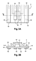
- the electronic module 5 is shown in plan view in FIG. 3A and in section along A-A in FIG. 3B.
- the module 5 comprises an insulating substrate 50 on one side of which is placed an integrated circuit 51.
- an etched metal layer forms electrical contact zones 52 whose dimensions correspond to those of a male plug. type A according to the USB standard.
- the layer forming the electrical contacts 52 may be thicker than for a conventional smart card to have a thickness corresponding to what is required by the USB standard. This thickness is possible because the thickness of the card body and even half a card body is greater than for an ISO 7816 format card.
- a second metal layer is placed on the same face of the substrate 50 as the integrated circuit 51 for producing conductive zones 53 of connection.
- the conductive zones 53 delimited by the dashed lines, extend, for example, over a large part of the surface of the insulating substrate in order to give the module 5 more rigidity.
- each conducting zone 53 passes over a contact zone 52 and has an edge near the integrated circuit 51 to electrically connect a contact pad of the integrated circuit 51 to each of the contact areas.
- a connecting wire 54 is crushed on the one hand on a contact pad and on the other hand on a conductive zone 53 to ensure the connection between the pad and said zone 53.
- metallized holes or conductive wells 55 pass through the substrate in order to make the electrical connection of each contact zone 52 to one of the conductive zones 53.
- One or more metallized holes may be made to connect a contact zone 52 to a conductive zone 53
- the integrated circuit 51 is then covered with a drop of resin and a protective pad 57, this covering technique being disclosed in the application EP-A-0 644 507 .
Landscapes
- Engineering & Computer Science (AREA)
- Computer Hardware Design (AREA)
- Microelectronics & Electronic Packaging (AREA)
- Physics & Mathematics (AREA)
- General Physics & Mathematics (AREA)
- Theoretical Computer Science (AREA)
- Credit Cards Or The Like (AREA)
Abstract
Une clef USB simplifiée 3 est réalisée en utilisant la technologie de fabrication d'une carte à puce 1. Les avantages de la carte à puce et de la clef USB sont alors réunis dans un seul produit. La carte à puce comporte un corps de carte 2 incluant une partie détachable 3 qui est munie d'une cavité 7 pour recevoir un module électronique 5 qui dispose de zones de contact électrique 52. La cavité 7 est pratiquée dans une zone de bordure de la partie détachable 3, ladite zone étant d'une largeur conforme au standard USB. Les zones de contact 52 sont conforment au standard USB. La partie détachable 3, une fois détachée, devient une clef USB enfichable dans un connecteur femelle USB de type A.
Description
- L'invention se rapporte à une carte à puce ayant une partie détachable qui se transforme en une clef USB enfichable dans un connecteur USB de type A
- Les clefs USB sont des objets portables conformes à la norme USB et destinés à être enfichés dans un connecteur USB femelle. Les clefs USB sont notamment utilisées avec des ordinateurs disposant d'au moins un port USB. D'un point de vu fonctionnel, les clefs USB sont utilisées comme mémoire de masse amovible ou comme élément de sécurisation permettant de crypter/décrypter des fichiers ou des messages échangés sur un réseau ouvert. Une clef USB comporte généralement un connecteur mâle conforme à la norme USB, un circuit imprimé incluant des composants électroniques et un ou plusieurs circuit intégré permettant d'assurer la fonction désirée de la clef, le tout étant enfermé dans un boîtier enfermant les circuits. Les clefs USB sont des objets assez coûteux en raison du nombre d'éléments à assembler.
- Parmi les objets portables conforme à la norme USB, il existe des cartes à puce selon la norme 7816 qui disposent d'une interface de communication de type USB. Ce type de carte est aussi décrit dans
EP-A-1 110 173 . Principalement, ce type de carte est réalisé avec un unique circuit intégré qui inclut un microprocesseur et une mémoire. De telles cartes sont destinées à des usages polyvalents utilisant des lecteurs ISO 7816 et des lecteurs USB. A titre d'exemple, dans le domaine de l'accès, une telle carte peut être utilisée pour l'accès physique à des bâtiments et l'accès à des réseaux de télécommunication de manière sécurisée. Un autre exemple d'utilisation peut être la carte bancaire utilisable pour le paiement sur un terminal de paiement ou par paiement sécurisé en ligne. Leur utilisation peut cependant être étendue à des fonctions autres sortant du registre de la sécurité et prenant appui sur les capacités de mémoire et de calcul du circuit intégré de la carte. - L'utilisateur peut insérer sa carte dans un terminal équipé d'un lecteur ISO 7816 ou dans un ordinateur muni d'un port USB de manière qu'une connexion électrique soit établie entre ledit terminal et les plages de contact de la carte. En pratique, ces cartes sont au format ISO ID1 (taille carte de crédit) et peuvent inclure une partie séparable au format ISO ID0 (taille mini carte pour téléphone mobile) comme montré sur la figure 1. Les plages de contact du module M de la carte sont configurée selon la norme 7816-2. En outre ce type de carte dispose d'une épaisseur de 800 µm.
- De par leur constitution, les rares cartes à puce fonctionnant selon le protocole USB ne sont pas directement enfichable dans un port USB et nécessitent un connecteur intermédiaire capable de recevoir une carte au format ISO ID1 et/ou une mini carte ISO ID0. A titre d'exemple, les demandes
EP-A-1 181 663 etEP-A-1 556 821 montrent des exemples de connecteur intermédiaire. - Les cartes à puces sont peu coûteuses en raison d'un nombre de composants peu élevé. Cependant cet avantage de prix diminue dès lors qu'il est nécessaire d'ajouter un connecteur intermédiaire.
- Un autre avantage des cartes à puce provient de leur facteur de forme plat qui est facilement imprimable. Une clef USB ayant un boîtier moulé est plus difficilement personnalisable et le coût d'une personnalisation d'un petit nombre de clef est nettement supérieur au coût pour une carte à puce.
- Le facteur de forme de la carte permet également de les distribuer par simple courrier postal ou à l'intérieur d'un magazine. Cela permet d'utiliser la carte comme support publicitaire associé à un petit contenu numérique. Le facteur de forme d'une clef USB conventionnelle ne permet pas d'avoir un tel mode de distribution. Cependant du fait du facteur de forme de la carte à puce, il n'est pas possible à un utilisateur de brancher celle-ci sur un ordinateur en l'absence d'un connecteur intermédiaire.
- Pour remédier aux problèmes précités, il est proposer de réaliser une clef USB simplifiée en utilisant la technologie de fabrication d'une carte à puce. Cela revient également à réaliser une carte à puce adaptée pour être directement utilisée dans un connecteur mâle USB de type A. Les avantages de la carte à puce et de la clef USB sont alors réunis dans un seul produit.
- L'invention est une carte à puce comportant un corps de carte et un module électronique. Le corps de carte inclut une partie détachable, une cavité étant réalisée sur une face dudit corps dans ladite partie détachable. Le module électronique inclut un substrat isolant, des zones de contact électrique placées sur une face dudit substrat et au moins un circuit intégré placé sur l'autre face dudit substrat. Le circuit intégré est électriquement relié aux zones de contact à travers le substrat. La cavité est pratiquée dans une zone de bordure de la partie détachable. Ladite zone est d'une largeur pouvant être introduite dans un connecteur au standard USB. Les zones de contact sont conforment à des zones de contact du standard USB. La partie détachable, une fois détachée, est une clef USB enfichable dans un connecteur femelle USB de type A.
- Préférentiellement, le module peut comporter également des zones conductrices placées sur la même face du substrat isolant que le circuit intégré, chacune desdites zones conductrices étant reliée à l'une des zones de contact par l'intermédiaire d'au moins un puit conducteur traversant le substrat isolant, ledit puit étant métallisé, et chacune desdites zones conductrices étant électriquement reliée à un plot de contact du circuit intégré. La partie détachable peut être maintenue au corps de carte par au moins deux attaches. Les attaches peuvent se trouver à des emplacements éloignés du module de sorte qu'aucun emplacement ne rentre dans un connecteur USB lorsque l'on enfiche la clef USB. Les attaches peuvent être dimensionnées pour rompre afin de séparer la partie détachable par une simple pression d'un doigt.
- L'invention sera mieux comprise, et d'autres particularités et avantages apparaîtront à la lecture de la description qui va suivre, la description faisant référence aux dessins annexés, parmi lesquels :
- la figure 1 montre une carte à puce compatible USB, selon l'état de la technique,
- les figures 2A à 2C montrent un mode de réalisation d'une clef USB selon l'invention,
- les figures 3A et 3B montrent un module selon l'invention,
- Le mode de réalisation de l'invention est décrit à l'aide de la figure 2 qui représente une carte à puce 1 en vue de face sur la figure 2A, en coupe transversale sur la figure 2B, et la clef USB après séparation sur la figure 2C.
- La carte à puce 1 comporte un corps de carte 2 incluant une partie détachable 3 reliée audit corps 2 par l'intermédiaire d'attaches 4. Les attaches 4 sont par exemple au nombre de quatre comme montré sur la figure 2A mais deux attaches pourraient suffire. Les attaches 4 sont suffisamment fine pour être sécable par simple pression du doigt afin de permettre une séparation aisée de la partie détachable 3.
- Le corps de carte 2 se présente sous la forme d'un parallélépipède rectangle dont les dimensions sont de l'ordre de 85,6 mm de longueur, 54 mm de largeur, et son épaisseur ε est comprise entre 2,055 mm et 2,415 mm, préférentiellement on choisira une valeur intermédiaire de 2,25 mm. Le corps de carte 2 est en plastique, thermoplastique ou thermodurcissable, par exemple constitué d'acrylonitrile butadiène styrène (ABS), de polychlorure de vinyle (PVC), de polyéthylène (PET) ou de poly-carbonates (PC). La découpe de séparation, entre le corps 2 et la partie détachable 3, et la formation des attaches 4 sont obtenus par emboutissage de la carte, découpage au laser, découpage au jet d'eau ou par moulage selon des procédés couramment utilisés dans la fabrication de cartes à puce. Les deux faces peuvent être imprimées avec un motif quelconque en utilisant tout procédé d'impression possible sur une carte, tel que par exemple offset, laser ou autre.
- Le corps de carte 2 comporte une cavité 7 placée à une extrémité de la partie séparable 3 pour recevoir un module électronique 5. Dans l'exemple préféré le module 5 est placé au même endroit que pour une carte conforme au standard ISO 7816 afin de pouvoir utiliser la même machine de placement. Le module est collé dans la cavité par exemple avec de la colle cyanoacrylate.
- La taille de la partie recevant le module ainsi que le module sont dimensionnés pour être à la taille du connecteur USB. Il est possible d'avoir un module de taille plus petite mais faire un fin rebord de plastique autour du module présente peu d'intérêt et complique la fabrication.
- Une différence majeure avec une carte à puce conventionnelle est l'épaisseur du corps de carte. Cependant, la différence d'épaisseur existant entre 800 µm et 2,25 permet d'utiliser les mêmes machine avec des réglages modifiés. Dans une variante, afin d'éviter d'avoir trop d'écart de réglage, et donc plus de rapidité d'adaptation dans une chaîne de fabrication, il est possible de réaliser le corps de carte 2 en deux demi-corps identiques qui sont ensuite collés l'un contre l'autre. Le collage peut être réalisé à chaud ou à froid selon une technique connue. La ligne pointillée 6 illustre cette variante de réalisation.
- Le module électronique 5 est montré en vue de dessus sur la figure 3A et en coupe selon A-A sur la figure 3B. Le module 5 comporte un substrat isolant 50 sur une face duquel est placé un circuit intégré 51. Sur une face opposée du substrat 50, une couche métallique gravée forme des zones de contact électrique 52 dont les dimensions correspondent à celles d'une fiche mâle de type A conforme au standard USB. La couche formant les contacts électriques 52 peut être plus épaisse que pour une carte à puce conventionnelle afin d'avoir une épaisseur correspondant à ce qui est requis par la norme USB. Cette sur épaisseur devient possible car l'épaisseur du corps de carte et même d'un demi-corps de carte est plus importante que pour une carte au format ISO 7816.
- Une deuxième couche métallique est placée sur la même face du substrat 50 que le circuit intégré 51 pour réaliser des zones conductrices 53 de liaison. Les zones conductrices 53, délimitées par les pointillés, s'étendent, par exemple, sur une grande partie de la surface du substrat isolant afin de donner plus de rigidité au module 5. En outre, chaque zone conductrice 53 passe au-dessus d'une zone de contact 52 et dispose d'un bord à proximité du circuit intégré 51 afin de relier électriquement un plot de contact du circuit intégré 51 à chacune des zones de contact. Un fil de liaison 54 est écrasé d'une part sur un plot de contact et d'autre part sur une zone conductrice 53 pour assurer la liaison entre le plot et ladite zone 53. Des trous métallisés ou puits conducteurs 55 traversent le substrat afin de réaliser la connexion électrique de chaque zone de contact 52 à l'une des zones conductrices 53. Un ou plusieurs trous métallisés peuvent être réalisés pour relier une zone de contact 52 à une zone conductrice 53. Le circuit intégré 51 est ensuite recouvert d'une goutte de résine et d'une pastille de protection 57, cette technique de recouvrement étant dévoilée dans la demande
EP-A-0 644 507 . - En variante, il est également possible de réaliser une connexion du circuit intégré 51 sur les zones conductrices avec une technologie de type Flip-Chip, également connue.
Claims (7)
- Carte à puce (1) comportant :- un corps de carte (2) incluant une partie détachable (3), une cavité (7) étant réalisée sur une face dudit corps dans ladite partie détachable, et- un module électronique (5) incluant un substrat isolant (50), des zones de contact électrique (52) placées sur une face dudit substrat et au moins un circuit intégré (51) placé sur l'autre face dudit substrat, le circuit intégré étant électriquement relié aux zones de contact à travers le substrat,caractérisé en ce que la cavité (7) est pratiquée dans une zone de bordure de la partie détachable (3), ladite zone étant d'une largeur pouvant être introduite dans un connecteur au standard USB, en ce que les zones de contact (52) sont conforment à des zones de contact du standard USB, et en ce que la partie détachable (3), une fois détachée, est une clef USB enfichable dans un connecteur femelle USB de type A.
- Carte à puce selon la revendication 1, dans laquelle le module (5) comporte également des zones conductrices (53) placées sur la même face du substrat isolant (50) que le circuit intégré (51), chacune desdites zones conductrices (53) étant reliée à l'une des zones de contact (52) par l'intermédiaire d'au moins un puit conducteur (55) traversant le substrat isolant (50), ledit puit (55) étant métallisé, et chacune desdites zones conductrices (53) étant électriquement reliée à un plot de contact du circuit intégré (51).
- Carte à puce selon la revendication 1 ou 2, dans laquelle la partie détachable (3) est maintenue au corps de carte (2) par au moins deux attaches (4).
- Carte à puce selon la revendication 3, dans laquelle les attaches (4) se trouvent à des emplacements éloignés du module de sorte qu'aucun emplacement ne rentre dans un connecteur USB lorsque l'on enfiche la clef USB.
- Carte à puce selon la revendication 3 ou 4, dans laquelle les attaches (4) sont dimensionnées pour rompre afin de séparer la partie détachable (3) par une simple pression d'un doigt.
- Carte à puce selon l'une des revendications précédentes, dans laquelle l'épaisseur du corps de carte (2) est comprise entre 2,055 mm et 2,415 mm.
- Carte à puce selon l'une des revendications précédentes, dans laquelle le module (5) est positionné sur le corps de carte (2) à une position correspondant à la norme ISO 7816.
Priority Applications (1)
| Application Number | Priority Date | Filing Date | Title |
|---|---|---|---|
| EP06300325A EP1843277A1 (fr) | 2006-04-04 | 2006-04-04 | Carte à puce USB |
Applications Claiming Priority (1)
| Application Number | Priority Date | Filing Date | Title |
|---|---|---|---|
| EP06300325A EP1843277A1 (fr) | 2006-04-04 | 2006-04-04 | Carte à puce USB |
Publications (1)
| Publication Number | Publication Date |
|---|---|
| EP1843277A1 true EP1843277A1 (fr) | 2007-10-10 |
Family
ID=36791829
Family Applications (1)
| Application Number | Title | Priority Date | Filing Date |
|---|---|---|---|
| EP06300325A Withdrawn EP1843277A1 (fr) | 2006-04-04 | 2006-04-04 | Carte à puce USB |
Country Status (1)
| Country | Link |
|---|---|
| EP (1) | EP1843277A1 (fr) |
Cited By (9)
| Publication number | Priority date | Publication date | Assignee | Title |
|---|---|---|---|---|
| WO2011015730A3 (fr) * | 2009-08-07 | 2011-06-30 | Emmanuel Thibaudeau | Dispositif de personnalisation de carte destinee a former un objet portable usb, carte associee, procede de detection de type de carte et utilisation des cartes dans un procede de publipostage |
| US8151345B1 (en) | 2007-01-25 | 2012-04-03 | Yeager C Douglas | Self-authorizing devices |
| US9082119B2 (en) | 2012-10-17 | 2015-07-14 | Royal Bank of Canada. | Virtualization and secure processing of data |
| US11080701B2 (en) | 2015-07-02 | 2021-08-03 | Royal Bank Of Canada | Secure processing of electronic payments |
| US11080700B2 (en) | 2015-01-19 | 2021-08-03 | Royal Bank Of Canada | Secure processing of electronic payments |
| US11210648B2 (en) | 2012-10-17 | 2021-12-28 | Royal Bank Of Canada | Systems, methods, and devices for secure generation and processing of data sets representing pre-funded payments |
| US11354651B2 (en) | 2015-01-19 | 2022-06-07 | Royal Bank Of Canada | System and method for location-based token transaction processing |
| US11599879B2 (en) | 2015-07-02 | 2023-03-07 | Royal Bank Of Canada | Processing of electronic transactions |
| US11961075B2 (en) | 2014-10-10 | 2024-04-16 | Royal Bank Of Canada | Systems for processing electronic transactions |
Citations (5)
| Publication number | Priority date | Publication date | Assignee | Title |
|---|---|---|---|---|
| EP1429283A2 (fr) * | 2002-12-12 | 2004-06-16 | Giesecke & Devrient GmbH | Support de données portatif |
| US20040259423A1 (en) * | 2001-09-24 | 2004-12-23 | Didier Elbaz | Dongle which is intended to be connected to a port of a telecommunications device |
| US6840454B1 (en) * | 1998-09-11 | 2005-01-11 | Schlumberger Systemes | Data transmission method and card therefor |
| DE102004039201A1 (de) * | 2004-08-12 | 2006-02-23 | Giesecke & Devrient Gmbh | Verfahren zur Herstellung eines tragbaren Datenträgers |
| FR2877461A1 (fr) * | 2004-11-02 | 2006-05-05 | Gemplus Sa | Dispositif electronique personnalise du type cle usb et procede de fabrication d'un tel dispositif |
-
2006
- 2006-04-04 EP EP06300325A patent/EP1843277A1/fr not_active Withdrawn
Patent Citations (5)
| Publication number | Priority date | Publication date | Assignee | Title |
|---|---|---|---|---|
| US6840454B1 (en) * | 1998-09-11 | 2005-01-11 | Schlumberger Systemes | Data transmission method and card therefor |
| US20040259423A1 (en) * | 2001-09-24 | 2004-12-23 | Didier Elbaz | Dongle which is intended to be connected to a port of a telecommunications device |
| EP1429283A2 (fr) * | 2002-12-12 | 2004-06-16 | Giesecke & Devrient GmbH | Support de données portatif |
| DE102004039201A1 (de) * | 2004-08-12 | 2006-02-23 | Giesecke & Devrient Gmbh | Verfahren zur Herstellung eines tragbaren Datenträgers |
| FR2877461A1 (fr) * | 2004-11-02 | 2006-05-05 | Gemplus Sa | Dispositif electronique personnalise du type cle usb et procede de fabrication d'un tel dispositif |
Cited By (14)
| Publication number | Priority date | Publication date | Assignee | Title |
|---|---|---|---|---|
| US8151345B1 (en) | 2007-01-25 | 2012-04-03 | Yeager C Douglas | Self-authorizing devices |
| US8548924B2 (en) | 2007-01-25 | 2013-10-01 | C. Douglas Yeager | Self-authorizing token |
| WO2011015730A3 (fr) * | 2009-08-07 | 2011-06-30 | Emmanuel Thibaudeau | Dispositif de personnalisation de carte destinee a former un objet portable usb, carte associee, procede de detection de type de carte et utilisation des cartes dans un procede de publipostage |
| CN102576422A (zh) * | 2009-08-07 | 2012-07-11 | E·蒂博多 | 用于产生便携式usb对象、相关联卡的卡个性化设备,用于检测卡的类型的方法,和卡在大批量邮寄方法中的使用 |
| US8628011B2 (en) | 2009-08-07 | 2014-01-14 | Emmanuel Thibaudeau | Card personalization device for producing a portable USB object, associated card, method for detecting the type of card, and use of the cards in a mass mailing method |
| US10755274B2 (en) | 2012-10-17 | 2020-08-25 | Royal Bank Of Canada | Virtualization and secure processing of data |
| US9082119B2 (en) | 2012-10-17 | 2015-07-14 | Royal Bank of Canada. | Virtualization and secure processing of data |
| US10846692B2 (en) | 2012-10-17 | 2020-11-24 | Royal Bank Of Canada | Virtualization and secure processing of data |
| US11210648B2 (en) | 2012-10-17 | 2021-12-28 | Royal Bank Of Canada | Systems, methods, and devices for secure generation and processing of data sets representing pre-funded payments |
| US11961075B2 (en) | 2014-10-10 | 2024-04-16 | Royal Bank Of Canada | Systems for processing electronic transactions |
| US11080700B2 (en) | 2015-01-19 | 2021-08-03 | Royal Bank Of Canada | Secure processing of electronic payments |
| US11354651B2 (en) | 2015-01-19 | 2022-06-07 | Royal Bank Of Canada | System and method for location-based token transaction processing |
| US11080701B2 (en) | 2015-07-02 | 2021-08-03 | Royal Bank Of Canada | Secure processing of electronic payments |
| US11599879B2 (en) | 2015-07-02 | 2023-03-07 | Royal Bank Of Canada | Processing of electronic transactions |
Similar Documents
| Publication | Publication Date | Title |
|---|---|---|
| EP1433125B1 (fr) | Clé électronique destinée à être connectée à un port d'un dispositif de télécommunication | |
| EP1779473B1 (fr) | Connecteur ameliore et dispositif pour systemes informatiques a connexion souple | |
| EP1810227B1 (fr) | Dispositif electronique personnalise du type cle usb et procede de fabrication d'un tel dispositif | |
| EP3223199B1 (fr) | Procédé de réalisation d'un module multifonctionnel et dispositif le comprenant | |
| FR2949011A1 (fr) | Carte destinee a former un organe informatique, et procedes de fabrication de cette carte et de cet organe informatique | |
| EP3734493B1 (fr) | Etui d'enrôlement pour carte à puce | |
| EP2194489A1 (fr) | Carte électronique ayant des moyens de commande | |
| EP3432221A1 (fr) | Carte électronique comprenant un capteur d'empreinte et procédé de fabrication d'une telle carte | |
| EP2118805B1 (fr) | Dispositif portable d'authentification | |
| EP2239691B1 (fr) | Ensemble à clé mémoire comprenant une carte à microcircuit | |
| FR2893436A1 (fr) | Securisation entre des composants electroniques d'une entite electronique securisee portable | |
| EP2045765B1 (fr) | Procédé de fabrication d'une clé électronique à connecteur USB | |
| WO2015158915A1 (fr) | Procédé de fabrication d'un dispositif à circuit électronique / électrique | |
| FR3128301A1 (fr) | Carte à puce avec capteur biométrique | |
| WO2016038313A1 (fr) | Dispositif electronique comportant un composant electronique presentant une zone d'affichage et procede de fabrication d'un tel dispositif | |
| EP1073998B1 (fr) | Procede de fabrication d'une carte a circuit integre a contact et une carte obtenue selon ce procede | |
| FR3045889A1 (fr) | Carte a puce du type a bouton poussoir et a batterie et un procede pour sa fabrication | |
| WO2000019368A1 (fr) | Carte a module secable | |
| WO2008004214A2 (fr) | Adaptateur électrique pouvant être couplé à une carte portable et carte portable solidaire dudit adaptateur | |
| EP2293226B1 (fr) | Dispositif électronique comprenant une carte à microcircuit | |
| FR2861483A1 (fr) | Procede de fabrication d'une cle electronique a connecteur usb et cle electronique obtenue | |
| FR2837594A1 (fr) | Objet portable a puce | |
| WO2002101641A1 (fr) | Carte à puce détachable sur support avec prédécoupe | |
| FR2817063A1 (fr) | Carte a memoire electronique microsim | |
| EP3471024A1 (fr) | Carte a puce avec module électronique sécurisé et procédé de fabrication |
Legal Events
| Date | Code | Title | Description |
|---|---|---|---|
| PUAI | Public reference made under article 153(3) epc to a published international application that has entered the european phase |
Free format text: ORIGINAL CODE: 0009012 |
|
| AK | Designated contracting states |
Kind code of ref document: A1 Designated state(s): AT BE BG CH CY CZ DE DK EE ES FI FR GB GR HU IE IS IT LI LT LU LV MC NL PL PT RO SE SI SK TR |
|
| AX | Request for extension of the european patent |
Extension state: AL BA HR MK YU |
|
| AKX | Designation fees paid | ||
| REG | Reference to a national code |
Ref country code: DE Ref legal event code: 8566 |
|
| STAA | Information on the status of an ep patent application or granted ep patent |
Free format text: STATUS: THE APPLICATION IS DEEMED TO BE WITHDRAWN |
|
| 18D | Application deemed to be withdrawn |
Effective date: 20080411 |