EP1841208A1 - Camera unit and imaging apparatus - Google Patents
Camera unit and imaging apparatus Download PDFInfo
- Publication number
- EP1841208A1 EP1841208A1 EP07006304A EP07006304A EP1841208A1 EP 1841208 A1 EP1841208 A1 EP 1841208A1 EP 07006304 A EP07006304 A EP 07006304A EP 07006304 A EP07006304 A EP 07006304A EP 1841208 A1 EP1841208 A1 EP 1841208A1
- Authority
- EP
- European Patent Office
- Prior art keywords
- support board
- ccd
- holder
- camera unit
- attachment
- Prior art date
- Legal status (The legal status is an assumption and is not a legal conclusion. Google has not performed a legal analysis and makes no representation as to the accuracy of the status listed.)
- Withdrawn
Links
- 238000003384 imaging method Methods 0.000 title claims abstract description 59
- 230000003287 optical effect Effects 0.000 claims abstract description 54
- 230000015572 biosynthetic process Effects 0.000 claims abstract description 27
- 238000001444 catalytic combustion detection Methods 0.000 description 123
- 125000006850 spacer group Chemical group 0.000 description 26
- 239000011521 glass Substances 0.000 description 20
- 239000006059 cover glass Substances 0.000 description 6
- 230000004044 response Effects 0.000 description 4
- 230000008859 change Effects 0.000 description 2
- 238000004519 manufacturing process Methods 0.000 description 2
- 239000005304 optical glass Substances 0.000 description 2
- 230000009467 reduction Effects 0.000 description 2
- 230000004048 modification Effects 0.000 description 1
- 238000012986 modification Methods 0.000 description 1
Images



Classifications
-
- H—ELECTRICITY
- H04—ELECTRIC COMMUNICATION TECHNIQUE
- H04N—PICTORIAL COMMUNICATION, e.g. TELEVISION
- H04N23/00—Cameras or camera modules comprising electronic image sensors; Control thereof
- H04N23/50—Constructional details
- H04N23/54—Mounting of pick-up tubes, electronic image sensors, deviation or focusing coils
-
- H—ELECTRICITY
- H04—ELECTRIC COMMUNICATION TECHNIQUE
- H04N—PICTORIAL COMMUNICATION, e.g. TELEVISION
- H04N23/00—Cameras or camera modules comprising electronic image sensors; Control thereof
- H04N23/50—Constructional details
- H04N23/55—Optical parts specially adapted for electronic image sensors; Mounting thereof
Definitions
- This invention relates to a camera unit and an imaging apparatus, and in particular to a camera unit that can use imaging devices different in thickness in the optical axis direction and image formation position, and an imaging apparatus including the camera unit.
- the image formation position of an optical image emitted from a lens unit becomes the same if the total thickness and refractive index of optical glass of dummy glass, an IR cut filter, cover glass for protecting the surface of an imaging device of a CCD, etc., are the same.
- An imaging device of a CCD, etc., and optical glass of dummy glass, cover glass, etc., are held in an imaging device holder included in a camera unit. If an attempt is made to hold imaging devices different in thickness in the optical axis direction and image formation position in the same imaging device holder, the optical axis direction position of the light reception surface of the imaging device for receiving an optical image emitted from a lens unit shifts and thus the light reception surface of the imaging device and the image formation position of the optical image do not match.
- An object of an illustrative, non-limiting embodiment of the invention is to provide a camera unit for making it possible to match the position of the light reception surface of an imaging device with the image formation position of an optical image from a lens unit if a plurality of imaging devices different in thickness in the optical axis direction and image formation position are held in a single imaging device holder and an imaging apparatus including the camera unit.
- a camera unit including: an imaging device that receives light of an optical image incident from a lens unit; a support board that supports the imaging device; and a holder having an attachment part to which the support board is attached.
- the attachment part of the holder and the support board has an irregularity part, and the irregularity part determines an attachment position an attachment position of the support board in an optical axis direction with respect to the holder so that a light reception surface of the imaging device matches an image formation position of the optical image.
- the position of the light reception surface of the imaging device can be matched with the image formation position of the optical image from the lens unit, so that it is not necessary to manufacture dedicated imaging device holders in a one-to-one correspondence with imaging devices different in thickness in the optical axis direction and image formation, and the cost of the mold charge, etc., can also be suppressed, resulting in a reduction in the cost.
- different support boards can be selectively attached to the attachment part of the holder in accordance with at least one of a thickness and the light reception surface of the imaging device.
- the irregularity part may comprises a protrusion part on the attachment part of the holder and a notch or through hole in the support board so as to avoid the protrusion part, the protrusion part and the notch or through hole fitting together to determine the attachment position of the support board.
- a first support board having the notch or through hole and a second support board not having the notch or through hole may be selectively attached to the attachment part of the holder.
- an imaging apparatus including the above-described camera unit.
- the position of the light reception surface of the imaging device can be matched with the image formation position of the optical image from the lens unit. Therefore, it is not necessary to manufacture dedicated imaging device holders in a one-to-one correspondence with imaging devices different in thickness in the optical axis direction and image formation, and the cost of the mold charge, etc., can also be suppressed, resulting in a reduction in the cost.
- FIGS. 1A and 1B are sectional views to show the general configuration of the imaging apparatus 10 according to the embodiment.
- the imaging apparatus 10 includes a camera unit 100 and a lens unit 200 that can be attached to and detached from the camera unit 100.
- the camera unit 100 includes main components of a first CCD 110A or a second CCD 110B as an example of an imaging device for receiving an optical image emitted from the lens unit 200, cover glass 120 for protecting the surface of the first CCD 110A or the second CCD 110B, dummy glass 130, a first spacer 140A or a second spacer 140B placed between the first CCD 110A or the second CCD 110B and the dummy glass 130, a holder 150 for holding the first CCD 110A or the second CCD 110B, the dummy glass 130, and the first spacer 140A or the second spacer 140B, and a first CCD support board 160A or a second CCD support board 160B on which the first CCD 11 0A or the second CCD 110B is installed.
- the dummy glass 130, the first spacer 140A (or the second spacer 140B), and the first CCD 110A (or the second CCD 110B) are arranged along an optical axis P direction in order from the front of the camera unit 100 (the side of the lens unit 200).
- the dummy glass 130 is sandwiched between the first spacer 140A (or the second spacer 140B) and the front end of the holder 150, whereby it is held or it is held by bonding.
- two types of CCDs namely, the first CCD 110A and the second CCD 110B different in thickness in the optical axis P direction can be selectively used as an imaging device of CCD, etc., that can be held in the holder 150.
- Two types of spacers, the first spacer 140A and the second spacer 1408 and two types of support boards, the first CCD support board 160A and the second CCD support board 160B are used in response to the two types of CCDs, the first CCD 110A and the second CCD 110B.
- FIG. 1 A shows the case where the first CCD 110A having a thin thickness in the optical axis P direction is used, and FIG.
- FIG. 1B shows the case where the second CCD 110B having a thick thickness in the optical axis P direction is used.
- the second CCD support board 160B is placed on a protrusion part 154 (155), as shown in FIG. 1B.
- the lens unit 200 has a plurality of, for example, two optical lenses 222 and 224 arranged in the optical axis P direction in a lens camera cone 210 to make up a lens optical system.
- An optical image emitted from the lens unit 200 is received at the first CCD 110A (or the second CCD 110B) and is formed at a focus position F.
- the first CCD 110A (or the second CCD 110B) is positioned so that the focus position F matches the position of the light reception surface of the first CCD 110A (or the second CCD 110B) in the optical axis P direction.
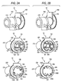
- FIG. 2A is a perspective view to show the configuration of the imaging apparatus 10 when the lens unit 200 is attached to the holder 150 according to the embodiment.
- FIG. 3A is a perspective view to show the configuration of the holder 150 according to the embodiment and
- FIG. 3B is a perspective view to show the configuration of the first CCD support board 160A according to the embodiment.
- the holder 150 is attached to the rear end of the lens camera cone 210 of the lens unit 200 (end part on the side of the camera unit 100).
- the holder 150 has an attachment part 151 to which the first CCD support board 160A or the second CCD support board 160B can be selectively attached at the rear of the holder 150 (opposite side of the lens unit 200).
- the first CCD support board 160A is attached to the attachment part 151.
- a hold part 152 for holding the dummy glass 130, the first spacer 140A, and the first CCD 110A is formed roughly at the center of the attachment part 151.
- the hold part 152 is made up of a first hold part 152b formed with an opening 152a for holding the dummy glass 130 and a second hold part 152c for holding the first spacer 140A.
- the attachment part 151 is formed on the inner periphery with two types of protrusion parts, a first protrusion part 154 and a second protrusion part 155.
- the first protrusion part 154 and the second protrusion part 155 are placed so as to become roughly symmetrical with respect to the center of the attachment part 151.
- the shapes, the number, and the layout of the protrusion parts 154 and 155 are not limited to those described above.
- a threaded hole 156 into which a fixing screw 156B for fixing the second CCD support board 160B attached to the attachment part 151 is fitted is formed so as to pierce the first protrusion part 154.
- the attachment part 151 is also formed with a threaded hole 158 into which a fixing screw 158A for fixing the first CCD support board 160A is fitted.
- two positioning pins 159 for positioning the first CCD support board 160A are provided on the attachment part 151 so as to become roughly symmetrical with respect to the center of the attachment part 151.
- the positions and the number of the threaded holes 156 and 158 and the positions, the shapes, and the number of the positioning pins 159 are not limited.
- the first CCD support board 160A is provided with engagement holes 162A and 164A for engaging the two positioning pins 159 and further is formed with two through holes 168A through which the fixing screws 158A pass.
- the first CCD support board 160A is formed with two notches 166A so as to avoid the first protrusion part 154 formed on the attachment part 151 of the holder 150 and two notches 167A so as to avoid the second protrusion part 155 when the first CCD support board 160A is attached to the attachment part 151 of the holder 150.
- the first CCD support board 160A and the first CCD 110A are formed in one piece by way of example.
- the first CCD support board 160A and the first CCD 110A need not necessarily be formed in one piece and the first CCD support board 160A may be formed in response to the thickness of the first CCD 110A in the optical axis P direction and the image formation position.
- FIGS. 4A and 4B are drawings to show a state in which the first CCD support board 160A is attached to the holder 150 according to the embodiment;
- FIG. 4A is a perspective view and
- FIG. 4B is a sectional view.
- first the positioning pins 159 and the engagement holes 162A and 164A are engaged with each other and the first CCD support board 160A in the attachment part 151 of the holder 150 is positioned, as shown in FIGS. 2A and 4A.
- the first CCD support board 160A has the notches 166A formed so as to avoid the first protrusion part 154 and the notches 167A formed so as to avoid the second protrusion part 155 and thus abuts faces 151a and 151b in the attachment part 151 (the positions of the faces 151a and 151b in the optical axis direction are the same) and the first CCD 110A is held.
- the first CCD support board 160A is positioned using the first protrusion part 154 and the second protrusion part 155 formed on the attachment part 151 of the holder 150 and the notches 166A and 167A formed in the first CCD support board 160A so as to avoid the first protrusion part 154 and the second protrusion part 155 in combination, but the invention is not limited to the combination of the protrusion parts and the notches.
- the first CCD support board 160A may be positioned using a protrusion part formed on the attachment part 151 of the holder 150 and a through hole made in the first CCD support board 160A so as to avoid the protrusion part.
- the protrusion part is not limited to the protrusion part formed on the attachment part 151 of the holder 150; the attachment position of the first CCD support board 160A in the optical axis P direction to the holder 150 may be determined by the irregularity part (i.e., the protrusion part, notch or through hole) formed on the attachment part 151 of the holder 150 or the first CCD support board 160A so that the light reception surface of the first CCD 110A matches the image formation position of an optical image from the lens unit 200.
- the irregularity part i.e., the protrusion part, notch or through hole
- FIG. 2B is a perspective view to show the configuration of the imaging apparatus 10 when the lens unit 200 is attached to the holder 150 according to the embodiment.
- FIG. 5A is a perspective view to show the configuration of the holder 150 according to the embodiment and
- FIG. 5B is a perspective view to show the configuration of the second CCD support board 160B according to the embodiment.
- the holder 150 As shown in FIG. 2B, the holder 150 according to the embodiment is attached to the rear end of the lens camera cone 210 of the lens unit 200 (end part on the side of the camera unit 100).
- the holder 150 has an attachment part 151 to which the first CCD support board 160A or the second CCD support board 1608 can be selectively attached at the rear of the holder 150 (opposite side of the lens unit 200).
- the second CCD support board 160B is attached to the attachment part 151.
- the hold part 152 for holding the dummy glass 130, the second spacer 140B, and the second CCD 110B is formed roughly at the center of the attachment part 151.
- the hold part 152 is made up of the first hold part 152b formed with the opening 152a for holding the dummy glass 130 and the second hold part 152c for holding the second spacer 140B.
- first protrusion part 154 The configuration of the first protrusion part 154, the second protrusion part 155, the threaded holes 156 and 158, the positioning pins 159, and the like has been described above in detail and therefore will not be discussed again.
- the second CCD support board 160B is provided with engagement holes 162B and 164B for engaging the two positioning pins 159 and further is formed with two through holes 168B through which the fixing screws 158B pass.
- the second CCD support board 160B is not formed with any notches or through holes so as to avoid the first protrusion part 154 and the second protrusion part 155 formed on the attachment part 151 of the holder 150 when the second CCD support board 160B is attached to the attachment part 151 of the holder 150.
- the second CCD support board 160B and the second CCD 110B are formed in one piece by way of example.
- the second CCD support board 160B and the second CCD 110B need not necessarily be formed in one piece and the second CCD support board 160B may be formed in response to the thickness of the second CCD 110B in the optical axis P direction and the image formation position.
- FIGS. 6A and 6B are drawings to show a state in which the second CCD support board 1608 is attached to the holder 150 according to the embodiment;
- FIG. 4A is a perspective view and
- FIG. 4B is a sectional view.
- the second CCD support board 160B does not have any notches or through holes formed so as to avoid the first protrusion part 154 and the second protrusion part 155 as described above and thus abuts the surface of the first protrusion part 154 and the surface of the second protrusion part 155 in the attachment part 151 (the positions of the surface of the first protrusion part 154 and the surface of the second protrusion part 155 in the optical axis direction are the same) and the second CCD 110B is held.
- the first CCD support board 160A and the second CCD support board 160B formed corresponding to the first CCD 110A and the second CCD 110B different in thickness in the optical axis P direction and image formation position can be selectively attached to the holder 150 and the shapes of the holder 150 and the two types of boards 160A and 160B are designed, whereby if the first CCD 110A and the second CCD 110B different in thickness in the optical axis P direction and image formation position are held in the same holder 150, the position of the light reception surface of the CCD 110A, 110B can be matched with the image formation position of the optical image from the lens unit 200.
- the first protrusion part 154 and the second protrusion part 155 are provided in the attachment part 151 of the holder 150 and the notches 166A and 167A formed so as to avoid the two types of protrusion parts 154 and 155 are provided in the first CCD support board 160A and not provided in the second CCD support board 160B, whereby if either of the first CCD 110A and the second CCD 110B different in thickness in the optical axis P direction and image formation position is used, the position of the light reception surface of the CCD 110A, 110B can be matched with the image formation position of the optical image from the lens unit 200.
- FIGS. 7A and 7B are sectional views to show the general configuration of the imaging apparatus 20 according to the embodiment.
- the shape of a spacer 140 is designed, specifically the spacer 140 is provided with a step 142, whereby the same spacer 140 can be used if two types of CCDs, a first CCD 110A and a second CCD 110B different in thickness in an optical axis P direction are used unlike the first embodiment described above.
- the same spacer 140 can be used for matching the position of the light reception surface of the CCD 110A, 110B with the image formation position of an optical image from a lens unit 200.
- the components other than the spacer 140 are similar to those of the first embodiment described above and therefore will not be discussed again.
- the thicknesses of the cover glass 120 and the dummy glass 130 are the same; however, if the sum total of the thicknesses of the cover glass 120 and the dummy glass 130 is the same, when imaging devices different in thickness in the optical axis direction and image formation position are used, the thickness of the cover glass 120 may differ from that of the dummy glass 130.
- the two types of support boards, the CCD support boards 160A and 160B formed in response to the two types of CCDs 110A and 110B different in thickness in the optical axis P direction can be selectively attached to the holder 150; however, the number of the types of support boards that can be attached to the holder is not limited to two and three or more types of support boards may be made able to be selectively attached to the holder.
Landscapes
- Engineering & Computer Science (AREA)
- Multimedia (AREA)
- Signal Processing (AREA)
- Studio Devices (AREA)
- Transforming Light Signals Into Electric Signals (AREA)
- Camera Bodies And Camera Details Or Accessories (AREA)
- Accessories Of Cameras (AREA)
Abstract
Description
- This invention relates to a camera unit and an imaging apparatus, and in particular to a camera unit that can use imaging devices different in thickness in the optical axis direction and image formation position, and an imaging apparatus including the camera unit.
- Generally, the image formation position of an optical image emitted from a lens unit becomes the same if the total thickness and refractive index of optical glass of dummy glass, an IR cut filter, cover glass for protecting the surface of an imaging device of a CCD, etc., are the same.
- An imaging device of a CCD, etc., and optical glass of dummy glass, cover glass, etc., are held in an imaging device holder included in a camera unit. If an attempt is made to hold imaging devices different in thickness in the optical axis direction and image formation position in the same imaging device holder, the optical axis direction position of the light reception surface of the imaging device for receiving an optical image emitted from a lens unit shifts and thus the light reception surface of the imaging device and the image formation position of the optical image do not match.
- Thus, hitherto, to use imaging devices different in thickness in the optical axis direction and image formation position, it has been necessary to use dedicated imaging device holders formed in a one-to-one correspondence with the imaging devices. (For example, refer to
JP-A-2005-326777 - However, if dedicated imaging device holders are manufactured in a one-to-one correspondence with imaging devices different in thickness in the optical axis direction and image formation, the cost of the mold charge, etc., much occurs, resulting in an increase in the cost.
- An object of an illustrative, non-limiting embodiment of the invention is to provide a camera unit for making it possible to match the position of the light reception surface of an imaging device with the image formation position of an optical image from a lens unit if a plurality of imaging devices different in thickness in the optical axis direction and image formation position are held in a single imaging device holder and an imaging apparatus including the camera unit.
- According to one aspect of the invention, there is provided a camera unit including: an imaging device that receives light of an optical image incident from a lens unit; a support board that supports the imaging device; and a holder having an attachment part to which the support board is attached. In the camera unit, at least one of the attachment part of the holder and the support board has an irregularity part, and the irregularity part determines an attachment position an attachment position of the support board in an optical axis direction with respect to the holder so that a light reception surface of the imaging device matches an image formation position of the optical image.
- According to the configuration, if a plurality of imaging devices different in thickness in the optical axis direction and image formation position are held in the same imaging device holder, the position of the light reception surface of the imaging device can be matched with the image formation position of the optical image from the lens unit, so that it is not necessary to manufacture dedicated imaging device holders in a one-to-one correspondence with imaging devices different in thickness in the optical axis direction and image formation, and the cost of the mold charge, etc., can also be suppressed, resulting in a reduction in the cost.
- In the camera unit, different support boards can be selectively attached to the attachment part of the holder in accordance with at least one of a thickness and the light reception surface of the imaging device.
- The irregularity part may comprises a protrusion part on the attachment part of the holder and a notch or through hole in the support board so as to avoid the protrusion part, the protrusion part and the notch or through hole fitting together to determine the attachment position of the support board.
- A first support board having the notch or through hole and a second support board not having the notch or through hole may be selectively attached to the attachment part of the holder.
- To the end, according to another aspect of the invention, there is provided an imaging apparatus including the above-described camera unit.
- The features of the invention will appear more fully upon consideration of the exemplary embodiment of the invention, which are schematically set forth in the drawings, in which:
- FIGS. 1A and 1B are sectional views to show an imaging apparatus according to a first exemplary embodiment of the invention;
- FIGS. 2A and 2B are perspective views to show the imaging apparatus in a state in which a lens unit is attached to a holder according to the first embodiment of the invention;
- FIG. 3A is a perspective view to show the holder according to the first embodiment of the invention, and FIG. 3B is a perspective view to show a first CCD support board according to the first embodiment of the invention;
- FIGS. 4A and 4B are drawings to show a state in which the first CCD support board according to the first embodiment of the invention is attached; FIG. 4A is a perspective view and FIG. 4B is a sectional view;
- FIG. 5A is a perspective view to show the holder according to the first embodiment of the invention, and FIG. 5B is a perspective view to show a second CCD support board according to the first embodiment of the invention;
- FIGS. 6A and 6B are drawings to show a state in which the second CCD support board according to the first embodiment of the invention is attached; FIG. 6A is a perspective view and FIG. 6B is a sectional view; and
- FIGS. 7A and 7B are sectional views to show an imaging apparatus according to a second exemplary embodiment of the invention.
- Although tie invention will be described below with reference to the exemplary embodiments thereof, the following exemplary embodiments and modifications do not restrict the invention.
- According to an exemplary embodiment, in the camera unit and the imaging apparatus including the camera unit, if a plurality of imaging devices different in thickness in the optical axis direction and image formation position are held in the same imaging device holder, the position of the light reception surface of the imaging device can be matched with the image formation position of the optical image from the lens unit. Therefore, it is not necessary to manufacture dedicated imaging device holders in a one-to-one correspondence with imaging devices different in thickness in the optical axis direction and image formation, and the cost of the mold charge, etc., can also be suppressed, resulting in a reduction in the cost.
- Exemplary embodiments of the invention will be discussed in detail with reference to the accompanying drawings. Components having substantially the same function are denoted by the same reference numeral in the Specification and the accompanying drawings and will not be discussed duplicately.
- To begin with, the configuration of an
imaging apparatus 10 according to a first exemplary embodiment of the invention will be discussed based on FIGS. 1A and 1B. FIGS. 1A and 1B are sectional views to show the general configuration of theimaging apparatus 10 according to the embodiment. - As shown in FIGS. 1A and 1B, the
imaging apparatus 10 includes acamera unit 100 and alens unit 200 that can be attached to and detached from thecamera unit 100. - The
camera unit 100 includes main components of afirst CCD 110A or asecond CCD 110B as an example of an imaging device for receiving an optical image emitted from thelens unit 200,cover glass 120 for protecting the surface of thefirst CCD 110A or thesecond CCD 110B,dummy glass 130, afirst spacer 140A or asecond spacer 140B placed between thefirst CCD 110A or thesecond CCD 110B and thedummy glass 130, aholder 150 for holding thefirst CCD 110A or thesecond CCD 110B, thedummy glass 130, and thefirst spacer 140A or thesecond spacer 140B, and a firstCCD support board 160A or a secondCCD support board 160B on which the first CCD 11 0A or thesecond CCD 110B is installed. - In the
holder 150, thedummy glass 130, thefirst spacer 140A (or thesecond spacer 140B), and thefirst CCD 110A (or thesecond CCD 110B) are arranged along an optical axis P direction in order from the front of the camera unit 100 (the side of the lens unit 200). In theholder 150, thedummy glass 130 is sandwiched between thefirst spacer 140A (or thesecond spacer 140B) and the front end of theholder 150, whereby it is held or it is held by bonding. - In the embodiment, two types of CCDs, namely, the
first CCD 110A and thesecond CCD 110B different in thickness in the optical axis P direction can be selectively used as an imaging device of CCD, etc., that can be held in theholder 150. Two types of spacers, thefirst spacer 140A and the second spacer 1408 and two types of support boards, the firstCCD support board 160A and the secondCCD support board 160B are used in response to the two types of CCDs, thefirst CCD 110A and thesecond CCD 110B. FIG. 1 A shows the case where thefirst CCD 110A having a thin thickness in the optical axis P direction is used, and FIG. 1B shows the case where thesecond CCD 110B having a thick thickness in the optical axis P direction is used. To use thesecond CCD 110B, the secondCCD support board 160B is placed on a protrusion part 154 (155), as shown in FIG. 1B. - The
lens unit 200 has a plurality of, for example, twooptical lenses lens camera cone 210 to make up a lens optical system. An optical image emitted from thelens unit 200 is received at thefirst CCD 110A (or thesecond CCD 110B) and is formed at a focus position F. In the embodiment, thefirst CCD 110A (or thesecond CCD 110B) is positioned so that the focus position F matches the position of the light reception surface of thefirst CCD 110A (or thesecond CCD 110B) in the optical axis P direction. - Next, the detailed configuration of the
holder 150 of thecamera unit 100 according to the embodiment and the positioning operation of thefirst CCD 110A (or thesecond CCD 110B) will be discussed based on FIGS. 2 to 6. - First, the configuration of the members when the
first CCD 110A is held by theholder 150 according to the embodiment will be discussed in detail based on FIGS. 2A and 3. FIG. 2A is a perspective view to show the configuration of theimaging apparatus 10 when thelens unit 200 is attached to theholder 150 according to the embodiment. FIG. 3A is a perspective view to show the configuration of theholder 150 according to the embodiment and FIG. 3B is a perspective view to show the configuration of the firstCCD support board 160A according to the embodiment. - As shown in FIG. 2A, the
holder 150 according to the embodiment is attached to the rear end of thelens camera cone 210 of the lens unit 200 (end part on the side of the camera unit 100). Theholder 150 has anattachment part 151 to which the firstCCD support board 160A or the secondCCD support board 160B can be selectively attached at the rear of the holder 150 (opposite side of the lens unit 200). To hold thefirst CCD 110A having a small thickness in the optical axis P direction, the firstCCD support board 160A is attached to theattachment part 151. - As shown in FIGS. 2A and 3A, a
hold part 152 for holding thedummy glass 130, thefirst spacer 140A, and thefirst CCD 110A is formed roughly at the center of theattachment part 151. Thehold part 152 is made up of afirst hold part 152b formed with anopening 152a for holding thedummy glass 130 and asecond hold part 152c for holding thefirst spacer 140A. - The
attachment part 151 is formed on the inner periphery with two types of protrusion parts, afirst protrusion part 154 and asecond protrusion part 155. Thefirst protrusion part 154 and thesecond protrusion part 155 are placed so as to become roughly symmetrical with respect to the center of theattachment part 151. The shapes, the number, and the layout of theprotrusion parts - A threaded
hole 156 into which a fixingscrew 156B for fixing the secondCCD support board 160B attached to theattachment part 151 is fitted is formed so as to pierce thefirst protrusion part 154. Theattachment part 151 is also formed with a threadedhole 158 into which a fixingscrew 158A for fixing the firstCCD support board 160A is fitted. Further, two positioningpins 159 for positioning the firstCCD support board 160A are provided on theattachment part 151 so as to become roughly symmetrical with respect to the center of theattachment part 151. The positions and the number of the threadedholes - As shown in FIGS. 2A and 3B, the first
CCD support board 160A is provided withengagement holes positioning pins 159 and further is formed with two throughholes 168A through which the fixing screws 158A pass. - The first
CCD support board 160A is formed with twonotches 166A so as to avoid thefirst protrusion part 154 formed on theattachment part 151 of theholder 150 and twonotches 167A so as to avoid thesecond protrusion part 155 when the firstCCD support board 160A is attached to theattachment part 151 of theholder 150. - In FIG. 3B, the first
CCD support board 160A and thefirst CCD 110A are formed in one piece by way of example. However, the firstCCD support board 160A and thefirst CCD 110A need not necessarily be formed in one piece and the firstCCD support board 160A may be formed in response to the thickness of thefirst CCD 110A in the optical axis P direction and the image formation position. - Next, the operation of attaching the first
CCD support board 160A to theattachment part 151 of theholder 150 according to the embodiment and the state after the attachment will be discussed in detail based on FIGS. 2A and 4. FIGS. 4A and 4B are drawings to show a state in which the firstCCD support board 160A is attached to theholder 150 according to the embodiment; FIG. 4A is a perspective view and FIG. 4B is a sectional view. - To attach the first
CCD support board 160A to theholder 150 holding thedummy glass 130 and thefirst spacer 140A, first the positioning pins 159 and theengagement holes CCD support board 160A in theattachment part 151 of theholder 150 is positioned, as shown in FIGS. 2A and 4A. - At this time, the first
CCD support board 160A has thenotches 166A formed so as to avoid thefirst protrusion part 154 and thenotches 167A formed so as to avoid thesecond protrusion part 155 and thus abutsfaces faces first CCD 110A is held. - Next, in this state, the fixing
screw 158A and the threadedhole 158 are fitted through the throughhole 168A, whereby the firstCCD support board 160A is fixed in theattachment part 151 and thedummy glass 130, thefirst spacer 140A, and thefirst CCD 110A are held in theholder 150 as shown in FIG. 4B. - In the embodiment, the first
CCD support board 160A is positioned using thefirst protrusion part 154 and thesecond protrusion part 155 formed on theattachment part 151 of theholder 150 and thenotches CCD support board 160A so as to avoid thefirst protrusion part 154 and thesecond protrusion part 155 in combination, but the invention is not limited to the combination of the protrusion parts and the notches. For example, the firstCCD support board 160A may be positioned using a protrusion part formed on theattachment part 151 of theholder 150 and a through hole made in the firstCCD support board 160A so as to avoid the protrusion part. The protrusion part is not limited to the protrusion part formed on theattachment part 151 of theholder 150; the attachment position of the firstCCD support board 160A in the optical axis P direction to theholder 150 may be determined by the irregularity part (i.e., the protrusion part, notch or through hole) formed on theattachment part 151 of theholder 150 or the firstCCD support board 160A so that the light reception surface of thefirst CCD 110A matches the image formation position of an optical image from thelens unit 200. - Next, the configuration of the members when the
second CCD 110B is held by theholder 150 according to the embodiment will be discussed in detail based on FIGS. 2B and 5. FIG. 2B is a perspective view to show the configuration of theimaging apparatus 10 when thelens unit 200 is attached to theholder 150 according to the embodiment. FIG. 5A is a perspective view to show the configuration of theholder 150 according to the embodiment and FIG. 5B is a perspective view to show the configuration of the secondCCD support board 160B according to the embodiment. - As shown in FIG. 2B, the
holder 150 according to the embodiment is attached to the rear end of thelens camera cone 210 of the lens unit 200 (end part on the side of the camera unit 100). Theholder 150 has anattachment part 151 to which the firstCCD support board 160A or the second CCD support board 1608 can be selectively attached at the rear of the holder 150 (opposite side of the lens unit 200). To hold thesecond CCD 110B, the secondCCD support board 160B is attached to theattachment part 151. - As shown in FIGS. 2B and 5A, the
hold part 152 for holding thedummy glass 130, thesecond spacer 140B, and thesecond CCD 110B is formed roughly at the center of theattachment part 151. Thehold part 152 is made up of thefirst hold part 152b formed with theopening 152a for holding thedummy glass 130 and thesecond hold part 152c for holding thesecond spacer 140B. - The configuration of the
first protrusion part 154, thesecond protrusion part 155, the threadedholes - As shown in FIGS. 2A and 3B, the second
CCD support board 160B is provided withengagement holes positioning pins 159 and further is formed with two through holes 168B through which the fixing screws 158B pass. - Unlike the first
CCD support board 160A, the secondCCD support board 160B is not formed with any notches or through holes so as to avoid thefirst protrusion part 154 and thesecond protrusion part 155 formed on theattachment part 151 of theholder 150 when the secondCCD support board 160B is attached to theattachment part 151 of theholder 150. - In FIG. 3B, the second
CCD support board 160B and thesecond CCD 110B are formed in one piece by way of example. However, the secondCCD support board 160B and thesecond CCD 110B need not necessarily be formed in one piece and the secondCCD support board 160B may be formed in response to the thickness of thesecond CCD 110B in the optical axis P direction and the image formation position. - Next, the operation of attaching the second
CCD support board 160B to theattachment part 151 of theholder 150 according to the embodiment and the state after the attachment will be discussed in detail based on FIGS. 2B and 6. FIGS. 6A and 6B are drawings to show a state in which the second CCD support board 1608 is attached to theholder 150 according to the embodiment; FIG. 4A is a perspective view and FIG. 4B is a sectional view. - To attach the second
CCD support board 160B to theholder 150 holding thedummy glass 130 and thesecond spacer 140B, first the positioning pins 159 and the engagement holes 162B and 164B are engaged with each other and the secondCCD support board 160B in theattachment part 151 of theholder 150 is positioned, as shown in FIGS. 2B and 6A. - At this time, the second
CCD support board 160B does not have any notches or through holes formed so as to avoid thefirst protrusion part 154 and thesecond protrusion part 155 as described above and thus abuts the surface of thefirst protrusion part 154 and the surface of thesecond protrusion part 155 in the attachment part 151 (the positions of the surface of thefirst protrusion part 154 and the surface of thesecond protrusion part 155 in the optical axis direction are the same) and thesecond CCD 110B is held. - Next, in this state, the fixing
screw 156B and the threadedhole 156 are fitted through the throughhole 166B, whereby the secondCCD support board 160B is fixed in theattachment part 151 and thedummy glass 130, thesecond spacer 140B, and thesecond CCD 110B are held in theholder 150 as shown in FIG. 6B. - As described above, in the embodiment, the first
CCD support board 160A and the secondCCD support board 160B formed corresponding to thefirst CCD 110A and thesecond CCD 110B different in thickness in the optical axis P direction and image formation position can be selectively attached to theholder 150 and the shapes of theholder 150 and the two types ofboards first CCD 110A and thesecond CCD 110B different in thickness in the optical axis P direction and image formation position are held in thesame holder 150, the position of the light reception surface of theCCD lens unit 200. Specifically, thefirst protrusion part 154 and thesecond protrusion part 155 are provided in theattachment part 151 of theholder 150 and thenotches protrusion parts CCD support board 160A and not provided in the secondCCD support board 160B, whereby if either of thefirst CCD 110A and thesecond CCD 110B different in thickness in the optical axis P direction and image formation position is used, the position of the light reception surface of theCCD lens unit 200. - The
imaging apparatus 10 according to the first embodiment of the invention has been described. Next, animaging apparatus 20 according to a second exemplary embodiment of the invention will be discussed based on FIGS. 7A and 7B. FIGS. 7A and 7B are sectional views to show the general configuration of theimaging apparatus 20 according to the embodiment. - In the
imaging apparatus 20, the shape of aspacer 140 is designed, specifically thespacer 140 is provided with astep 142, whereby thesame spacer 140 can be used if two types of CCDs, afirst CCD 110A and asecond CCD 110B different in thickness in an optical axis P direction are used unlike the first embodiment described above. - That is, to use the
first CCD 110A having a small thickness in the optical axis P direction,dummy glass 130 is abutted against a face other than thestep 142 of thespacer 140; to use thesecond CCD 110B having a large thickness in the optical axis P direction,dummy glass 130 is abutted against thestep 142 of thespacer 140, whereby if the two types of CCDs, thefirst CCD 110A and thesecond CCD 110B different in thickness in the optical axis P direction are used, thesame spacer 140 can be used for matching the position of the light reception surface of theCCD lens unit 200. - The components other than the
spacer 140 are similar to those of the first embodiment described above and therefore will not be discussed again. - Although the preferred embodiments of the invention have been described with reference to the accompanying drawings, the invention is not limited to the specific embodiments, needless to say. Those skilled in the art will recognize that various change examples or modified examples of such embodiments exist. Such change examples or modified examples are intended to be within the scope of the invention and the appended claims.
- For example, in the description of the embodiment, the thicknesses of the
cover glass 120 and thedummy glass 130 are the same; however, if the sum total of the thicknesses of thecover glass 120 and thedummy glass 130 is the same, when imaging devices different in thickness in the optical axis direction and image formation position are used, the thickness of thecover glass 120 may differ from that of thedummy glass 130. - For example, in the description of the embodiment, the two types of support boards, the
CCD support boards CCDs holder 150; however, the number of the types of support boards that can be attached to the holder is not limited to two and three or more types of support boards may be made able to be selectively attached to the holder. - While the invention has been described with reference to the exemplary embodiments, the technical scope of the invention is not restricted to the description of the exemplary embodiments. It is apparent to the skilled in the art that various changes or improvements can be made. It is apparent from the description of claims that the changed or improved configurations can also be included in the technical scope of the invention.
- This application claims foreign priority from
Japanese Patent Application No. 2006-87898, filed March 28, 2006
Claims (7)
- A camera unit comprising:an imaging device that receives light of an optical image incident from a lens unit;a support board that supports the imaging device; anda holder having an attachment part to which the support board is attached,wherein
at least one of the attachment part of the holder and the support board has an irregularity part, the irregularity part determining an attachment position an attachment position of the support board in an optical axis direction with respect to the holder so that a light reception surface of the imaging device matches an image formation position of the optical image. - The camera unit according to claim 1, wherein different support boards can be selectively attached to the attachment part of the holder in accordance with at least one of a thickness and the light reception surface of the imaging device.
- The camera unit according to claim 1, wherein the irregularity part comprises a protrusion part on the attachment part of the holder and a notch or through hole in the support board so as to avoid the protrusion part, the protrusion part and the notch or through hole fitting together to determine the attachment position of the support board.
- The camera unit according to claim 3 wherein a first support board having the notch or through hole and a second support board not having the notch or through hole can be selectively attached to the attachment part of the holder.
- The camera unit according to claim 2, wherein the irregularity part comprises a protrusion part on the attachment part of the holder and a notch or through hole in the support board so as to avoid the protrusion part, the protrusion part and the notch or through hole fitting together to determine the attachment position of the support board.
- The camera unit according to claim 5 wherein a first support board having the notch or through hole and a second support board not having the notch or through hole can be selectively attached to the attachment part of the holder.
- An imaging apparatus comprising a camera unit according to claim 1.
Applications Claiming Priority (1)
| Application Number | Priority Date | Filing Date | Title |
|---|---|---|---|
| JP2006087898A JP4714619B2 (en) | 2006-03-28 | 2006-03-28 | Camera device and imaging device |
Publications (1)
| Publication Number | Publication Date |
|---|---|
| EP1841208A1 true EP1841208A1 (en) | 2007-10-03 |
Family
ID=38234343
Family Applications (1)
| Application Number | Title | Priority Date | Filing Date |
|---|---|---|---|
| EP07006304A Withdrawn EP1841208A1 (en) | 2006-03-28 | 2007-03-27 | Camera unit and imaging apparatus |
Country Status (6)
| Country | Link |
|---|---|
| US (1) | US7961243B2 (en) |
| EP (1) | EP1841208A1 (en) |
| JP (1) | JP4714619B2 (en) |
| KR (1) | KR100907267B1 (en) |
| CN (1) | CN101046598B (en) |
| TW (1) | TW200736689A (en) |
Families Citing this family (1)
| Publication number | Priority date | Publication date | Assignee | Title |
|---|---|---|---|---|
| TWI432167B (en) * | 2011-10-04 | 2014-04-01 | Medimaging Integrated Solution Inc | Host, optical lens module and digital diagnostic system including the same |
Citations (5)
| Publication number | Priority date | Publication date | Assignee | Title |
|---|---|---|---|---|
| JPH1051670A (en) | 1996-07-29 | 1998-02-20 | Shinji Misaki | Adapter for ccd back for view camera |
| US5861654A (en) * | 1995-11-28 | 1999-01-19 | Eastman Kodak Company | Image sensor assembly |
| JP2002330321A (en) * | 2001-05-01 | 2002-11-15 | Mitsubishi Electric Corp | Solid-state imaging device and camera |
| US6628339B1 (en) | 1999-06-14 | 2003-09-30 | Eastman Kodak Company | Image sensor mount for a digital camera |
| JP2005326777A (en) | 2004-05-17 | 2005-11-24 | Fujinon Corp | Lens barrel |
Family Cites Families (4)
| Publication number | Priority date | Publication date | Assignee | Title |
|---|---|---|---|---|
| US6122009A (en) | 1995-05-31 | 2000-09-19 | Sony Corporation | Image pickup apparatus fabrication method thereof image pickup adaptor apparatus signal processing apparatus signal processing method thereof information processing apparatus and information processing method |
| JP3498775B2 (en) * | 1995-05-31 | 2004-02-16 | ソニー株式会社 | Imaging device |
| JP2001245217A (en) * | 2000-03-02 | 2001-09-07 | Olympus Optical Co Ltd | Small imaging module |
| JP2005284147A (en) * | 2004-03-30 | 2005-10-13 | Fuji Photo Film Co Ltd | Imaging device |
-
2006
- 2006-03-28 JP JP2006087898A patent/JP4714619B2/en not_active Expired - Lifetime
-
2007
- 2007-03-27 EP EP07006304A patent/EP1841208A1/en not_active Withdrawn
- 2007-03-27 CN CN2007100884750A patent/CN101046598B/en active Active
- 2007-03-27 KR KR1020070029641A patent/KR100907267B1/en not_active Expired - Fee Related
- 2007-03-28 TW TW096110692A patent/TW200736689A/en not_active IP Right Cessation
- 2007-03-28 US US11/727,811 patent/US7961243B2/en active Active
Patent Citations (5)
| Publication number | Priority date | Publication date | Assignee | Title |
|---|---|---|---|---|
| US5861654A (en) * | 1995-11-28 | 1999-01-19 | Eastman Kodak Company | Image sensor assembly |
| JPH1051670A (en) | 1996-07-29 | 1998-02-20 | Shinji Misaki | Adapter for ccd back for view camera |
| US6628339B1 (en) | 1999-06-14 | 2003-09-30 | Eastman Kodak Company | Image sensor mount for a digital camera |
| JP2002330321A (en) * | 2001-05-01 | 2002-11-15 | Mitsubishi Electric Corp | Solid-state imaging device and camera |
| JP2005326777A (en) | 2004-05-17 | 2005-11-24 | Fujinon Corp | Lens barrel |
Also Published As
| Publication number | Publication date |
|---|---|
| KR100907267B1 (en) | 2009-07-13 |
| CN101046598B (en) | 2011-03-16 |
| TW200736689A (en) | 2007-10-01 |
| CN101046598A (en) | 2007-10-03 |
| US7961243B2 (en) | 2011-06-14 |
| JP4714619B2 (en) | 2011-06-29 |
| KR20070097341A (en) | 2007-10-04 |
| TWI359964B (en) | 2012-03-11 |
| JP2007266887A (en) | 2007-10-11 |
| US20070229701A1 (en) | 2007-10-04 |
Similar Documents
| Publication | Publication Date | Title |
|---|---|---|
| US8582020B2 (en) | Imaging apparatus with a camera body whereon an interchangeable lens can be removably mounted | |
| JP5871534B2 (en) | Imaging device | |
| JP6931979B2 (en) | Lens holding mechanism and imaging device | |
| EP1841208A1 (en) | Camera unit and imaging apparatus | |
| CN113219766B (en) | Reflection module and camera module including reflection module | |
| JP2009071631A (en) | Camera module | |
| JP2007094359A (en) | Prism fixing method | |
| US7834311B2 (en) | Lens assembly with a rotatable adjustable member for discretely varying position of a mounting member | |
| KR102354711B1 (en) | Interchangeable lens and camera system | |
| JP2009258296A (en) | Finder structure for single lens reflex camera | |
| US12174447B2 (en) | Lens device | |
| JP2021167907A (en) | Manufacturing method of image pickup device and image pickup device | |
| JP6197843B2 (en) | Virtual image display device | |
| JP2007017698A (en) | Reflective optics assembly unit | |
| JP2007147729A (en) | Camera module | |
| JP7382271B2 (en) | Imaging device | |
| JP7182265B2 (en) | Attachments, lens systems, electronics systems, and camera systems | |
| JP2011107417A (en) | Lens barrel and imaging device | |
| JP2019028416A (en) | Imaging apparatus | |
| JP2005134833A (en) | Imaging device and imaging device | |
| JP2008258813A (en) | Camera module | |
| KR20240111280A (en) | Camera module | |
| JP4844312B2 (en) | Lens barrel, optical equipment | |
| JP2023127287A (en) | Optical filter unit and imaging device | |
| JP2000330158A (en) | Finder device |
Legal Events
| Date | Code | Title | Description |
|---|---|---|---|
| PUAI | Public reference made under article 153(3) epc to a published international application that has entered the european phase |
Free format text: ORIGINAL CODE: 0009012 |
|
| 17P | Request for examination filed |
Effective date: 20070327 |
|
| AK | Designated contracting states |
Kind code of ref document: A1 Designated state(s): AT BE BG CH CY CZ DE DK EE ES FI FR GB GR HU IE IS IT LI LT LU LV MC MT NL PL PT RO SE SI SK TR |
|
| AX | Request for extension of the european patent |
Extension state: AL BA HR MK YU |
|
| AKX | Designation fees paid |
Designated state(s): AT BE BG CH CY CZ DE DK EE ES FI FR GB GR HU IE IS IT LI LT LU LV MC MT NL PL PT RO SE SI SK TR |
|
| RAP1 | Party data changed (applicant data changed or rights of an application transferred) |
Owner name: FUJIFILM CORPORATION |
|
| STAA | Information on the status of an ep patent application or granted ep patent |
Free format text: STATUS: THE APPLICATION IS DEEMED TO BE WITHDRAWN |
|
| 18D | Application deemed to be withdrawn |
Effective date: 20131001 |